Embed Size (px)
Citation preview

© Biricha Digital Power LtdParkway DrReadingRG4 6XG – UKApril - 2018
1
Dr Ali Shirsavar
Biricha Digital Power Ltd
EMI Filter Design Example
This is a very small 1 hour session based on our 2 Day EMI Filter Design
Workshop

• PSU Specification‒ Input voltage Vin = 12V
‒ Output power Pout = 6.75W
‒ Efficiency =85%
‒ PSU closed loop input impedance Zin = 18
‒ Desired single stage filter output impedance Zo = Zin/10 < 2
‒ Input current Iin = Vin/Zin = 660mA
‒ Switching frequency Fs = 200kHz
‒ Lowest frequency of interest Fh = 200kHz
‒ Harmonic number of Fh n = 1
‒ PSU Loop cross over frequency Fx = 2kHz
‒ Reflected Ripple Current** @ Fh (no filtering, simulated) Irr_RMS = 760mA
‒ Estimated Duty / = 42%
‒ Reflected Ripple Current @ Fh (no filtering, calculated) Irr_RMS=
‒ Source Inductance L_source = 100uH (standard LISN)
• Filter Specification‒ Desired Irr after filtering Irr_filtered_RMS = 100dBuV (i.e. 2mA)
‒ Gain of single stage filter @ Fh Gain_2ndorder = 0.05
‒ single stage filter cut-off of frequency Fc/o = 10.3kHz
‒ Desired cut-off frequency of common mode filter Fc/o_CM = 75kHz
𝐺𝑎𝑖𝑛2𝑛𝑑_𝑜𝑟𝑑𝑒𝑟@𝑓 =𝐷𝑒𝑠𝑖𝑟𝑒𝑑 𝐴𝑚𝑝𝑙𝑖𝑡𝑢𝑑𝑒 𝑎𝑓𝑡𝑒𝑟 𝑓𝑖𝑙𝑡𝑒𝑟𝑖𝑛𝑔
𝐴𝑚𝑝𝑙𝑖𝑡𝑢𝑑𝑒 𝑏𝑒𝑓𝑜𝑟𝑒 𝑓𝑖𝑙𝑡𝑒𝑟𝑖𝑛𝑔=𝑓𝑐/𝑜𝑓
© Biricha Digital Power 2018
𝐹𝑝𝑖 ≅ 1 2𝜋 𝐿_𝑠𝑜𝑢𝑟𝑐𝑒||𝐿1 × 𝐶𝑝𝑖𝐹_𝐸𝑆𝑅0 =1
2𝜋 𝐶1 𝐸𝑆𝑅𝐶1
𝑓𝑐/𝑜 =1
2 𝜋 𝐿𝐶
𝑄 ≅1
𝑅
𝐿
𝐶
𝑍𝑖𝑛 ≈𝑉𝑖𝑛2 𝜂
𝑃𝑜𝑢𝑡
Cpi Rules:1 2 3
Fc/o_CM = 1
2𝜋 𝐿𝐶𝑀1 𝐶𝐶𝑀1
Note 1: We have 2 CM capsNote 2: Typically 1 decade below where CM noise starts
½ L1
C1
Chassis
Cpi
L_source
L_CM1
2 x ½ C_CM1
Rd
Cd
½ L1
𝐶1 ≅𝐶𝑑
5
𝑍𝑜 =𝐿∗
𝐶
DC/DC Single Stage CM & DM EMI Filter Design Cheat Sheet
𝑑𝐵𝜇𝑉 𝑡𝑜 𝐴𝑚𝑝𝑠 = 10𝑉𝑜𝑙𝑡𝑎𝑔𝑒 𝑖𝑛 𝑑𝐵𝜇𝑉
201𝜇𝑉
50Ω=
Where L = L1 , C = C1, R = Rd
* L = L_source + L1 for worse case Zo calculations only** Reflected ripple current with no filtering is the same as Input Terminal Ripple Current
𝐼𝑟𝑟_𝑛𝑡ℎ_𝐻𝑎𝑟𝑚𝑜𝑛𝑖𝑐_𝑅𝑀𝑆 =0.45
𝑛
𝑃𝑜𝑢𝑡
𝑉𝑖𝑛 ×𝑒𝑓𝑓𝑖𝑐𝑖𝑒𝑛𝑦×𝐷𝑠𝑖𝑛 𝑛 × 180𝑜 × 𝐷

• Single Cell/Stage LC EMI Specification
‒ Min Capacitance C1_min = 8uF
‒ Max Capacitance C1_max = 20uF
‒ Min Inductance L1_min = 10uH
‒ Max Inductance L1_max = 30uH
‒ Selected C1 & Part No = 1 x 10uF + (3 x 4.7uF on-board)
‒ Total C1 after DC Bias Loss = 7.1uF + 12.3uF = ~20uF
‒ Combined ESR of C1 @ Fs = ~1m
‒ Frequency of ESR Zero due to C1 F_ESR0 = 8MHz
‒ Selected L1 & Part No = ~10uH
‒ Actual Fc/o = 10kHz
‒ Actual Zo (not including L_source) = 0.7
‒ Actual Zo (including L_source) = 2.3
‒ Calculated Damping Cap Cd =
‒ Calculated Damping Resistor Rd =
‒ Actual Damping Cap Cd = 100uF
‒ Actual Damping R Rd = 0.42
‒ Q (not including L_source) = 1.7
‒ Q (including L_source) = 5.6
C1_min
L1_min
C1_max
L1_max
DC/DC Single Stage CM & DM EMI Filter Design Example
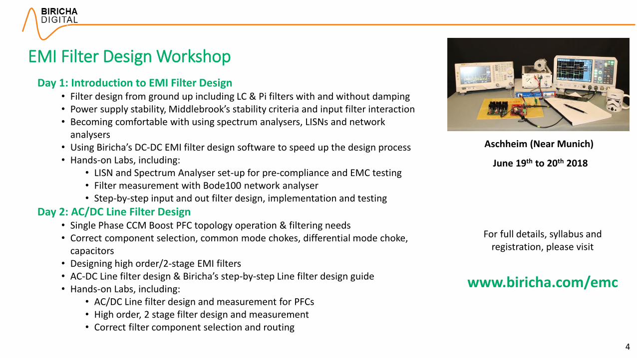
EMI Filter Design Workshop
4
Day 1: Introduction to EMI Filter Design• Filter design from ground up including LC & Pi filters with and without damping• Power supply stability, Middlebrook’s stability criteria and input filter interaction• Becoming comfortable with using spectrum analysers, LISNs and network
analysers• Using Biricha’s DC-DC EMI filter design software to speed up the design process• Hands-on Labs, including:
• LISN and Spectrum Analyser set-up for pre-compliance and EMC testing • Filter measurement with Bode100 network analyser• Step-by-step input and out filter design, implementation and testing
Day 2: AC/DC Line Filter Design• Single Phase CCM Boost PFC topology operation & filtering needs• Correct component selection, common mode chokes, differential mode choke,
capacitors• Designing high order/2-stage EMI filters• AC-DC Line filter design & Biricha’s step-by-step Line filter design guide • Hands-on Labs, including:
• AC/DC Line filter design and measurement for PFCs• High order, 2 stage filter design and measurement • Correct filter component selection and routing
Aschheim (Near Munich)
June 19th to 20th 2018
For full details, syllabus and registration, please visit
www.biricha.com/emc
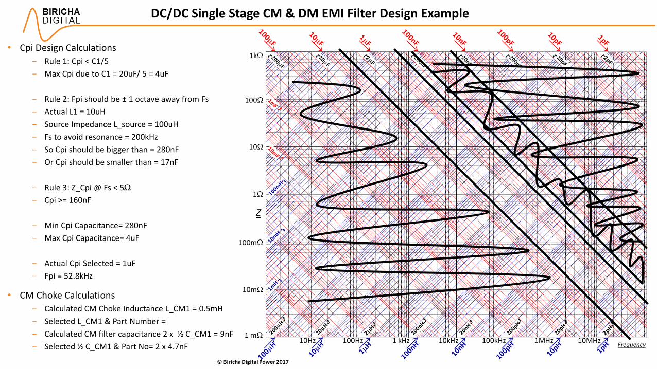
• Cpi Design Calculations
‒ Rule 1: Cpi < C1/5
‒ Max Cpi due to C1 = 20uF/ 5 = 4uF
‒ Rule 2: Fpi should be ± 1 octave away from Fs
‒ Actual L1 = 10uH
‒ Source Impedance L_source = 100uH
‒ Fs to avoid resonance = 200kHz
‒ So Cpi should be bigger than = 280nF
‒ Or Cpi should be smaller than = 17nF
‒ Rule 3: Z_Cpi @ Fs < 5
‒ Cpi >= 160nF
‒ Min Cpi Capacitance= 280nF
‒ Max Cpi Capacitance= 4uF
‒ Actual Cpi Selected = 1uF
‒ Fpi = 52.8kHz
• CM Choke Calculations
‒ Calculated CM Choke Inductance L_CM1 = 0.5mH
‒ Selected L_CM1 & Part Number =
‒ Calculated CM filter capacitance 2 x ½ C_CM1 = 9nF
‒ Selected ½ C_CM1 & Part No= 2 x 4.7nF
DC/DC Single Stage CM & DM EMI Filter Design Example