Embed Size (px)
Citation preview

From Technologies to Market
Sample
© 2019
Emerging Semiconductor
Substrates: Market and Technology
Trends 2019
2
GLOSSARY & ACRONYMS(1/2)
• LDMOS : Laterally Depleted Metal Oxide Semiconductor
• AGR :Annual Growth Rate
• AlN:Aluminum Nitride
• APD:Avalanche Photo Diode
• AR:Augmented Reality
• ASP :Average Selling Price
• BAW : Bulk Acoustic Wave
• Bi-CMOS : Bipolar and CMOS process technology
• BICMOS: Bipolar-CMOS
• BIFET: Bi Field Effect Transistor
• BFM: Baligas figure of merit
• BOM: Bill Of Materials
• BTS : Base Transceiver Station
• CdTe: CadmiumTellurium
• CIGS: Copper-Indium-Gallium-Selenium
• CMOS: Complementary Metal-on silicon Oxide
Semiconductor
• CTE: Coefficient of thermal expansion
• CZ: Czochralski
• DBR: Distributed Bragg Reflector
• DFB: Distributed Feedback Laser
• DHBT: Double Heterojunction Bipolar Transistor
• DU: Distributed Unit
• EEL: Edge Emitting Laser
• EML: Electro-absorption Modulated Laser
• EPD: Etch Pitch Density• EFG: Edge defined film fed• FEM : Front-End Module• FET : Field Effect Transistor• FFTx: Fiber to the x• FIR: Far Infrared• FM : Frequency Modulation• F-P: Fabry Pérot• FS: Free Standing• FTIR: Fourier-transform infrared spectroscopy• FTTH: Fiber to the Home• FZ: Floating Zone• GaAs: Gallium Arsenide• GaN: Gallium Nitride• Ga2O3: Gallium Oxide• GaSb: Gallium Antimonide• HB: Horizontal Bridgman,• HBT : Heterojunction Bipolar Transistor• HE: High End• HEMT : High Electron Mobility Transistor• HPHT: High pressure high temperature• HVPE: Hydride vapor phase epitaxy• IC : Integrated Circuit• InSb: Indium Antimonide• InP: Indium Phosphide• InPOGaAs: InP-on-GaAs• IR: Infrared• JFM: Johnson Figure of Merit
Emerging Semiconductor Substrates: Market and Technology Trends | Sample | www.yole.fr | ©2019
3
GLOSSARY & ACRONYMS (2/2)
• JFET: Junction field effect transistor
• KFM: Keyes figure of merit
• LD: Laser diode
• LEC: Liquid Encapsulated Czochralski
• LED: Light Emitting Diode
• LIDAR: Light Detection and Ranging
• LNA : Low Noise Amplifier
• LPE: Liquid Phase Epitaxy
• LWIR: Long Wave Infrared
• MBE: Molecular Beam Epitaxy
• MCM : Multi-Chip Module
• MEMS : Micro-Electro-Mechanical System
• MESFET: Metal Semiconductor Field Effect Transistor
• MEMOCVD: Migration-enhanced metal-organic chemical vapor deposition
• MIMO: Multiple Input, Multiple Output
• MMIC: Monolithic Microwave Integrated Circuit
• MOCVD: Metalorganic Chemical Vapor Deposition
• MOHVPE: Metal organic hydride vapor phase epitaxy
• MQW: Multiple Quantum Wells
• MWCVD : Microwave enhanced CVD
• MWIR: Medium Wave IR
• MLED: MicroLED
• NIR: Near IR
• ODM : Original Design Manufacturer
• OEM : Original Equipment Manufacturer
• PA: Power Amplifier• PAE: Power Added Efficiency• PD: Photodiode• POI: Piezo on Insulator• PVDNC: Plasma vapor deposition of nanocolumns • RADAR : Radio Detection And Ranging• RFFE: RF Front-End• RWG: Ridge waveguide • SC: Semi Conductive• SBD: Schottky barrier diode• SHBT : Single Heterojunction Bipolar Transistor • SI: Semi Insulative• SiC: Silicon Carbide• SiGe: Silicon Germanium• SiPH: Silicon Photonics• SOI: Silicon-on-Insulator• SWIR: Short Wave IR• TD : Threading dislocation• THz: Terahertz • TIA: Transimpedance Amplifier • T2SL:Type-2 Superlattice • UPS: Uninterruptible power supply• VB: Vertical Bridgman• VCSEL: Vertically Cavity Surface Emitting Laser• VGF: Vertical Gradient Freeze• VISAR: Video Synthetic Aperture Radar • VR: Virtual Reality
Emerging Semiconductor Substrates: Market and Technology Trends | Sample | www.yole.fr | ©2019
4
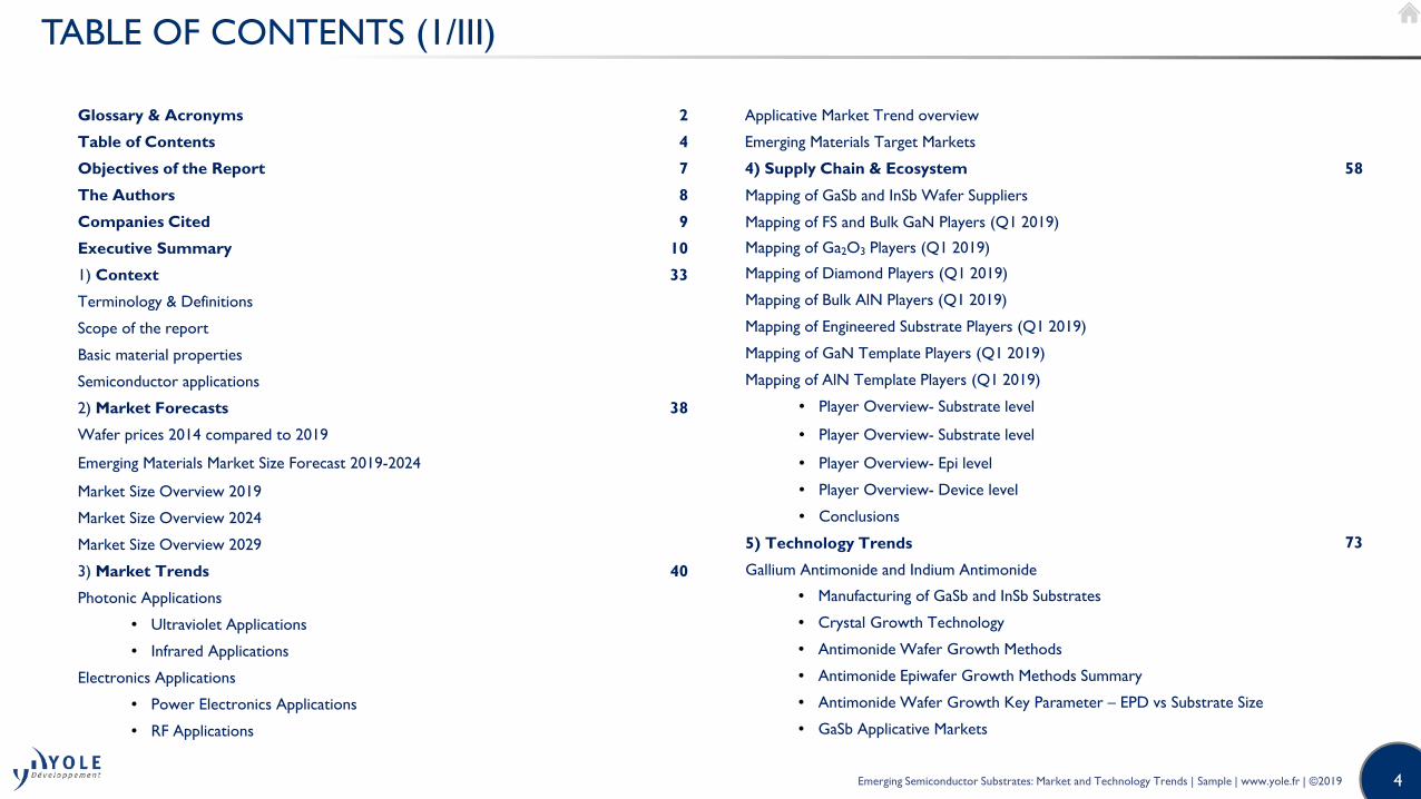
TABLE OF CONTENTS (1/III)
Glossary & Acronyms 2
Table of Contents 4
Objectives of the Report 7
The Authors 8
Companies Cited 9
Executive Summary 10
1) Context 33
Terminology & Definitions
Scope of the report
Basic material properties
Semiconductor applications
2) Market Forecasts 38
Wafer prices 2014 compared to 2019
Emerging Materials Market Size Forecast 2019-2024
Market Size Overview 2019
Market Size Overview 2024
Market Size Overview 2029
3) Market Trends 40
Photonic Applications
• Ultraviolet Applications
• Infrared Applications
Electronics Applications
• Power Electronics Applications
• RF Applications
Applicative Market Trend overview
Emerging Materials Target Markets
4) Supply Chain & Ecosystem 58
Mapping of GaSb and InSb Wafer Suppliers
Mapping of FS and Bulk GaN Players (Q1 2019)
Mapping of Ga2O3 Players (Q1 2019)
Mapping of Diamond Players (Q1 2019)
Mapping of Bulk AlN Players (Q1 2019)
Mapping of Engineered Substrate Players (Q1 2019)
Mapping of GaN Template Players (Q1 2019)
Mapping of AlN Template Players (Q1 2019)
• Player Overview- Substrate level
• Player Overview- Substrate level
• Player Overview- Epi level
• Player Overview- Device level
• Conclusions
5) Technology Trends 73
Gallium Antimonide and Indium Antimonide
• Manufacturing of GaSb and InSb Substrates
• Crystal Growth Technology
• Antimonide Wafer Growth Methods
• Antimonide Epiwafer Growth Methods Summary
• Antimonide Wafer Growth Key Parameter – EPD vs Substrate Size
• GaSb Applicative Markets
Emerging Semiconductor Substrates: Market and Technology Trends | Sample | www.yole.fr | ©2019

5
TABLE OF CONTENTS (II/III)
• Infrared Laser / Detection Applications
• IR Imaging Technologies
• GaSb Applicative Markets Use Cases
• Future Evolution of GaSb Based Devices
• InSb Applicative Markets
• InSb Devices Use Cases
• Future Evolution of InSb Based Devices
• GaSb and InSb Devices: Status Summary and Time to Market Discussion
• Conclusions
Free Standing and Bulk GaN 94
• Bulk GaN Substrate Orientation
• Free Standing and Bulk GaN Overview
• Growth Methods – A Note on Flatness: FS vs True Bulk substrate
• History and Time line
• Key Manufacturing Steps for FS & Bulk GaN Wafer
• Bulk GaN Growth Methods Summary
• Separation Techniques for FS Wafers
• Wafer Finishing
• Main Specifications of Players
• Status and Trends
• FS and Bulk GaN Requirement for Different Market Segments
• GaN-on-GaN Laser Diode Market
• GaN-on-GaN LED
• GaN-on-GaN Power Device
• Status Summary and Time to Market Discussion
• Conclusions
Gallium Oxide 122
• History and Time Line
• β-Ga2O3 bulk Growth Methods Summary
• β-Ga2O3 bulk Growth Examples
• β-Ga2O3 Wafer Examples
• Ga2O3 Epiwafer Growth Methods Summary
• Ga2O3 potential application Summary
• Ga2O3 Device
• Status Summary and Time to Market Discussion
• Conclusions
Diamond 133
• Diamond R&D and Technology Roadmap
• Diamond Single-Crystal Growth
• Comparison of Diamond Substrates
• HPHT and MW CVD Growth
• Diamond Wafer Fabrication
• Mosaic Single Crystal Wafer Fabrication
• Hetero-epitaxial Single Crystal Diamond Technology
• Diamond Applicative Markets
• Diamond for Power and Rf Electronics Applications
• Diamond as Active Heat Sink Substrate
• Diamond Magnetic / Electric Field Sensors
• Diamond Detectors
• Status Summary and Time to Market Discussion
• Conclusions
Emerging Semiconductor Substrates: Market and Technology Trends | Sample | www.yole.fr | ©2019
6
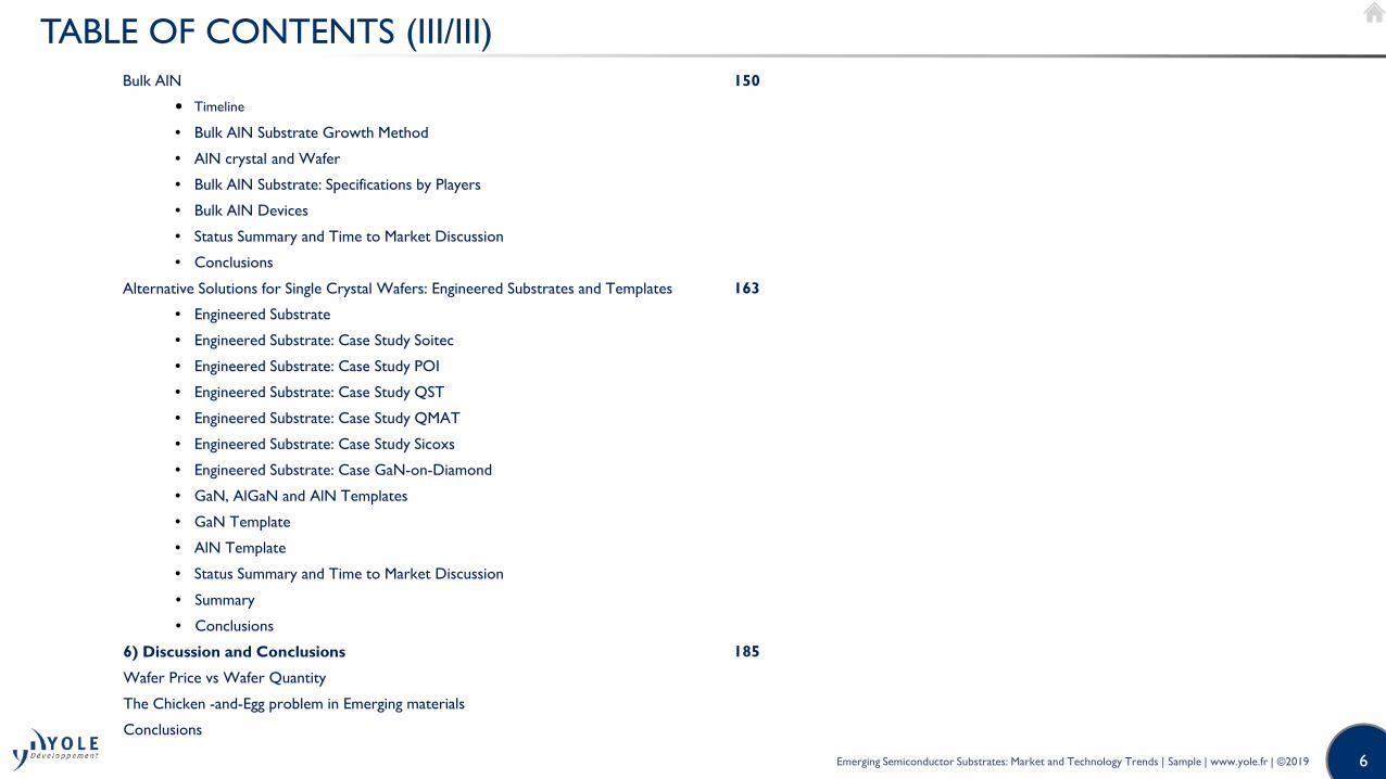
TABLE OF CONTENTS (III/III)
Bulk AlN 150
• Timeline
• Bulk AlN Substrate Growth Method
• AlN crystal and Wafer
• Bulk AlN Substrate: Specifications by Players
• Bulk AlN Devices
• Status Summary and Time to Market Discussion
• Conclusions
Alternative Solutions for Single Crystal Wafers: Engineered Substrates and Templates 163
• Engineered Substrate
• Engineered Substrate: Case Study Soitec
• Engineered Substrate: Case Study POI
• Engineered Substrate: Case Study QST
• Engineered Substrate: Case Study QMAT
• Engineered Substrate: Case Study Sicoxs
• Engineered Substrate: Case GaN-on-Diamond
• GaN, AlGaN and AlN Templates
• GaN Template
• AlN Template
• Status Summary and Time to Market Discussion
• Summary
• Conclusions
6) Discussion and Conclusions 185
Wafer Price vs Wafer Quantity
The Chicken -and-Egg problem in Emerging materials
Conclusions
Emerging Semiconductor Substrates: Market and Technology Trends | Sample | www.yole.fr | ©2019
7
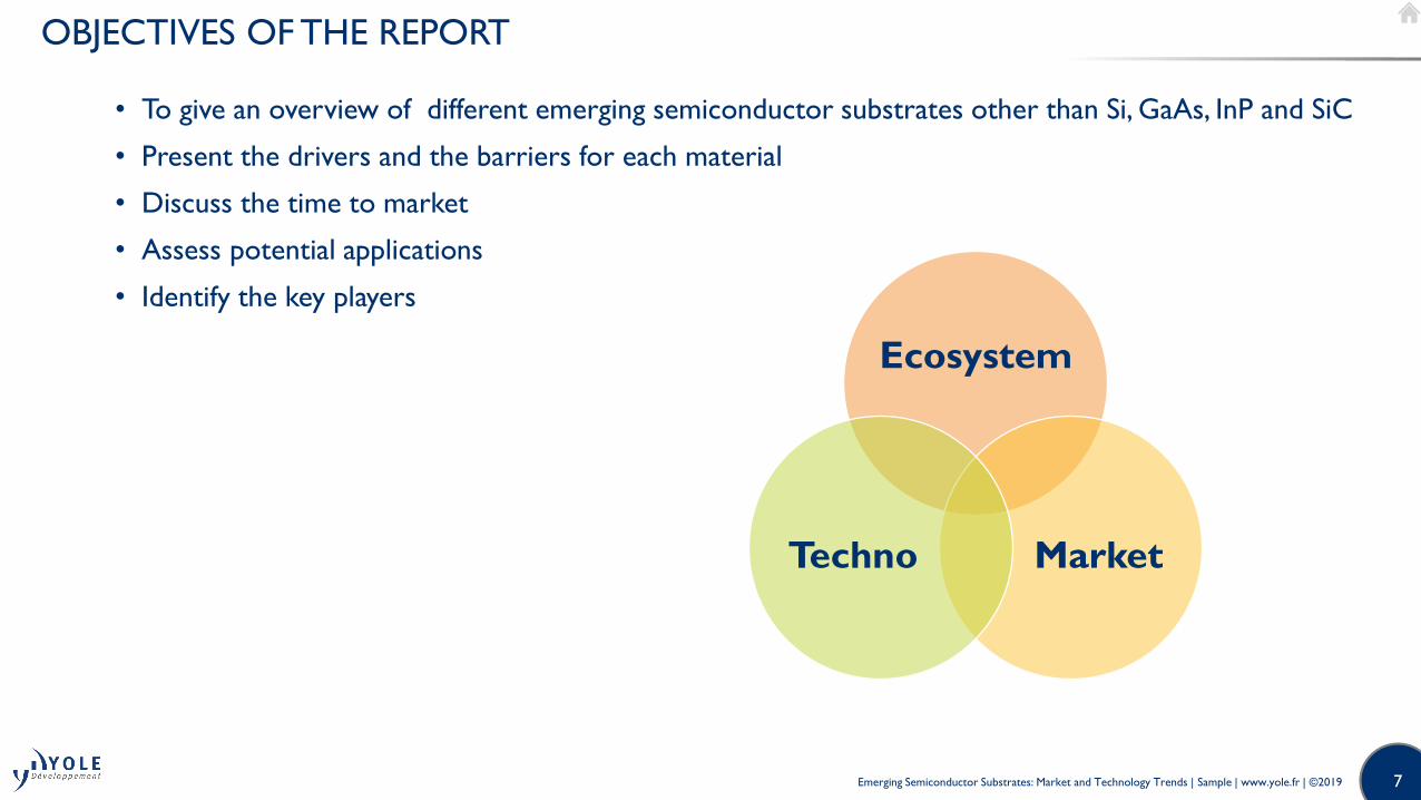
OBJECTIVES OF THE REPORT
• To give an overview of different emerging semiconductor substrates other than Si, GaAs, InP and SiC
• Present the drivers and the barriers for each material
• Discuss the time to market
• Assess potential applications
• Identify the key players
Ecosystem
MarketTechno
Emerging Semiconductor Substrates: Market and Technology Trends | Sample | www.yole.fr | ©2019
8
Biographies & contacts
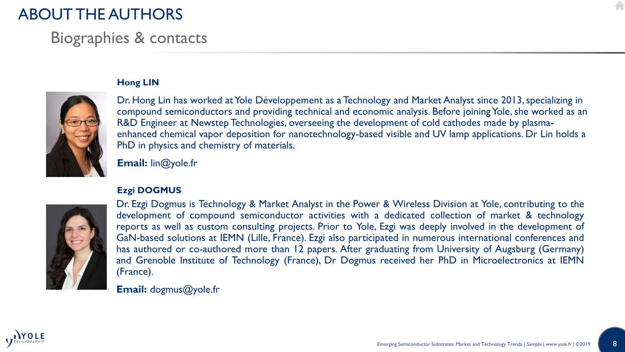
ABOUT THE AUTHORS
Ezgi DOGMUS
Dr. Hong Lin has worked at Yole Développement as a Technology and Market Analyst since 2013, specializing in compound semiconductors and providing technical and economic analysis. Before joining Yole, she worked as an R&D Engineer at Newstep Technologies, overseeing the development of cold cathodes made by plasma-enhanced chemical vapor deposition for nanotechnology-based visible and UV lamp applications. Dr Lin holds a PhD in physics and chemistry of materials.
Email: [email protected]
Dr. Ezgi Dogmus is Technology & Market Analyst in the Power & Wireless Division at Yole, contributing to thedevelopment of compound semiconductor activities with a dedicated collection of market & technologyreports as well as custom consulting projects. Prior to Yole, Ezgi was deeply involved in the development ofGaN-based solutions at IEMN (Lille, France). Ezgi also participated in numerous international conferences andhas authored or co-authored more than 12 papers. After graduating from University of Augsburg (Germany)and Grenoble Institute of Technology (France), Dr Dogmus received her PhD in Microelectronics at IEMN(France).
Email: [email protected]
Hong LIN
Emerging Semiconductor Substrates: Market and Technology Trends | Sample | www.yole.fr | ©2019
9
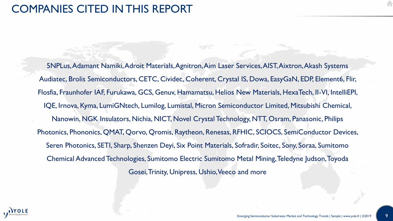
COMPANIES CITED IN THIS REPORT
5NPLus, Adamant Namiki, Adroit Materials, Agnitron, Aim Laser Services, AIST, Aixtron, Akash Systems
Audiatec, Brolis Semiconductors, CETC, Cividec, Coherent, Crystal IS, Dowa, EasyGaN, EDP, Element6, Flir,
Flosfia, Fraunhofer IAF, Furukawa, GCS, Genuv, Hamamatsu, Helios New Materials, HexaTech, II-VI, IntelliEPI,
IQE, Irnova, Kyma, LumiGNtech, Lumilog, Lumistal, Micron Semiconductor Limited, Mitsubishi Chemical,
Nanowin, NGK Insulators, Nichia, NICT, Novel Crystal Technology, NTT, Osram, Panasonic, Philips
Photonics, Phononics, QMAT, Qorvo, Qromis, Raytheon, Renesas, RFHIC, SCIOCS, SemiConductor Devices,
Seren Photonics, SETI, Sharp, Shenzen Deyi, Six Point Materials, Sofradir, Soitec, Sony, Soraa, Sumitomo
Chemical Advanced Technologies, Sumitomo Electric Sumitomo Metal Mining, Teledyne Judson, Toyoda
Gosei, Trinity, Unipress, Ushio, Veeco and more
Emerging Semiconductor Substrates: Market and Technology Trends | Sample | www.yole.fr | ©2019
10
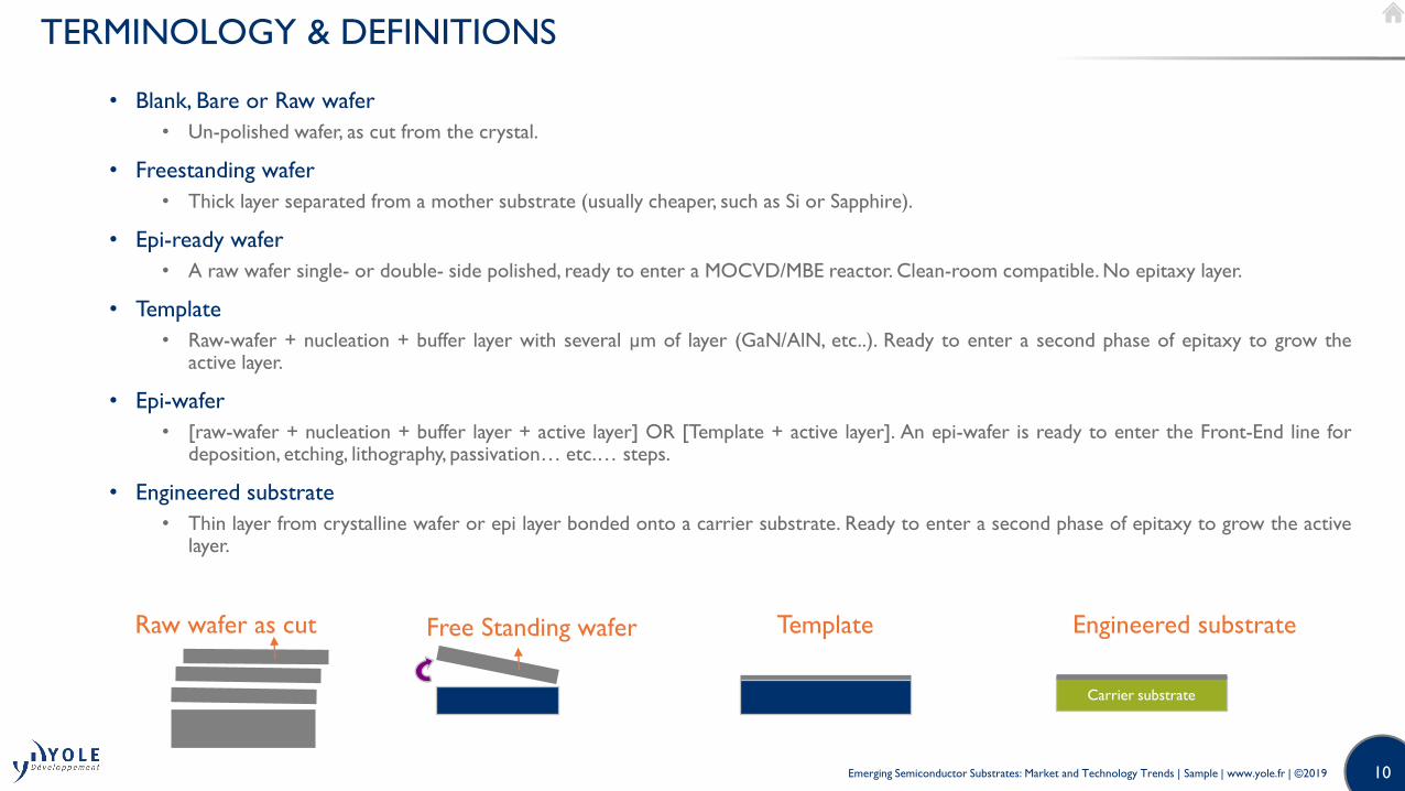
TERMINOLOGY & DEFINITIONS
• Blank, Bare or Raw wafer
• Un-polished wafer, as cut from the crystal.
• Freestanding wafer
• Thick layer separated from a mother substrate (usually cheaper, such as Si or Sapphire).
• Epi-ready wafer
• A raw wafer single- or double- side polished, ready to enter a MOCVD/MBE reactor. Clean-room compatible. No epitaxy layer.
• Template
• Raw-wafer + nucleation + buffer layer with several µm of layer (GaN/AlN, etc..). Ready to enter a second phase of epitaxy to grow theactive layer.
• Epi-wafer
• [raw-wafer + nucleation + buffer layer + active layer] OR [Template + active layer]. An epi-wafer is ready to enter the Front-End line fordeposition, etching, lithography, passivation… etc.… steps.
• Engineered substrate
• Thin layer from crystalline wafer or epi layer bonded onto a carrier substrate. Ready to enter a second phase of epitaxy to grow the activelayer.
Carrier substrate
Raw wafer as cut Free Standing wafer Template Engineered substrate
Emerging Semiconductor Substrates: Market and Technology Trends | Sample | www.yole.fr | ©2019

11
WHAT IS IN THIS REPORT?
• In this report, we give an overview of the emerging crystalline semiconductor substrates, including GaSb,InSb, GaN, Ga2O3, AlN and diamond. Except for diamond, the materials are all compoundsemiconductors.
• We do NOT include some other compound semiconductors, such as SiC, GaAs and InP, which are wellestablished and covered in various reports by Yole. We also do NOT include SiGe, which ismanufactured on silicon wafers using conventional silicon processing toolsets.
• As these emerging wafers are costly, there have been numerous developments by academics andindustry to develop low cost alternative solutions, such as templates or engineering substrates. In thiscontext, we also include in this report the GaN template,AlN template and engineered substrates.
• We present our understanding on the developmental status/maturity of these materials and theirapplication potential for both photonic and electronics applications, including laser diode, LED,sensor/detector, power electronics and RF. We do not look at PV applications, which is a very maturemarket.
Emerging Semiconductor Substrates: Market and Technology Trends | Sample | www.yole.fr | ©2019
12
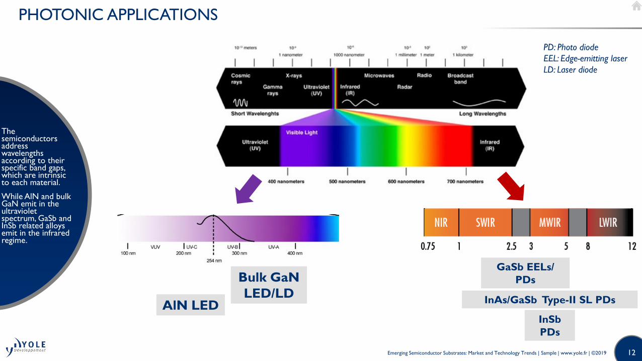
PHOTONIC APPLICATIONS
The semiconductors address wavelengths according to their specific band gaps, which are intrinsic to each material.
While AlN and bulk GaN emit in the ultraviolet spectrum, GaSb and InSb related alloys emit in the infrared regime.
Bulk GaN
LED/LDAlN LED
GaSb EELs/
PDs
InAs/GaSb Type-II SL PDs
InSb
PDs
PD: Photo diode
EEL: Edge-emitting laser
LD: Laser diode
Emerging Semiconductor Substrates: Market and Technology Trends | Sample | www.yole.fr | ©2019
13
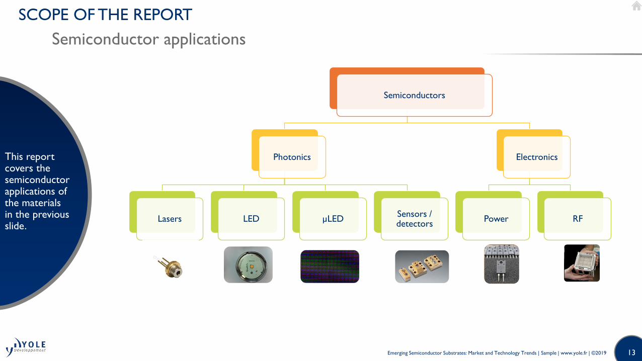
SCOPE OF THE REPORT
Semiconductor applications
This report covers the semiconductor applications of the materials in the previous slide.
Semiconductors
Photonics
Lasers LED µLEDSensors / detectors
Electronics
Power RF
Emerging Semiconductor Substrates: Market and Technology Trends | Sample | www.yole.fr | ©2019
14
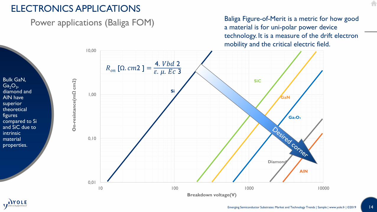
ELECTRONICS APPLICATIONS
Power applications (Baliga FOM)
Bulk GaN, Ga2O3, diamond and AlN have superior theoretical figures compared to Si and SiC due to intrinsic material properties.
0,01
0,10
1,00
10,00
10 100 1000 10000
On
-resi
stan
ce(m
Ω c
m2)
Breakdown voltage(V)
Si
SiC
GaN
Ga2O3
Diamond
AlN
Baliga Figure-of-Merit is a metric for how good
a material is for uni-polar power device
technology. It is a measure of the drift electron
mobility and the critical electric field.
𝑅𝑜𝑛 [Ω. 𝑐𝑚2 ] =4. 2.ߝ .ߤ 𝑐ܧ 3
Emerging Semiconductor Substrates: Market and Technology Trends | Sample | www.yole.fr | ©2019
15
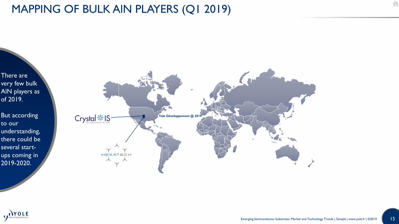
MAPPING OF BULK AlN PLAYERS (Q1 2019)
There are
very few bulk
AlN players as
of 2019.
But according
to our
understanding,
there could be
several start-
ups coming in
2019-2020.
Yole Développement @ 2019
Emerging Semiconductor Substrates: Market and Technology Trends | Sample | www.yole.fr | ©2019
16
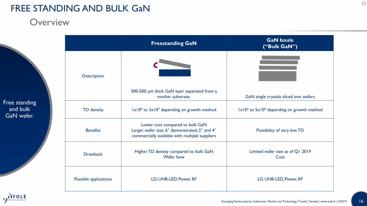
FREE STANDING AND BULK GaN
Overview
Free standing and bulk
GaN wafer.
Freestanding GaNGaN boule
(“Bulk GaN”)
Description
300-500 µm thick GaN layer separated from a
mother substrate. GaN single crystals sliced into wafers
TD density 1x10⁴ to 5x10⁷ depending on growth method 1x10³ to 5x10⁴ depending on growth method
Benefits
Lower cost compared to bulk GaN
Larger wafer size, 6” demonstrated, 2” and 4”
commercially available with multiple suppliers
Possibility of very low TD
DrawbackHigher TD density compared to bulk GaN
Wafer bow
Limited wafer size as of Q1 2019
Cost
Possible applications LD, UHB-LED, Power, RF LD, UHB-LED, Power, RF
Emerging Semiconductor Substrates: Market and Technology Trends | Sample | www.yole.fr | ©2019

17
DIAMOND
Introduction
Diamond is a dream material with high thermal conductivity, band gap, electrical isolation, high electron mobility and radiation hardness.
Synthetic single crystal diamonds have been developed for a long time now, yet still faces limited size and high cost.
• Diamond material development began more than 50 years
ago. Besides traditional tooling applications (drilling, cutting,
etc.), interest in diamonds continues to grow for both
optical and thermal applications, as well as for new
semiconductor device applications such as high-power, high-
frequency devices able to work at elevated temperatures.
• Diamond’s unique physical and electrical properties, which
include the highest-known thermal conductivity, a wide band
gap, excellent electrical insulator properties, very high
breakdown voltage and very high carrier mobility, make
diamond an excellent candidate for creating electronic
devices with superior performance.
• The availability of diamond materials such as high-quality,
large-size single-crystal wafers and thick polycrystalline films,
and the decrease of their still-high manufacturing costs, are
crucial milestones for diamond electronic device
development and detection / sensing applications.
Jewelry
For
electronics or
detection
Emerging Semiconductor Substrates: Market and Technology Trends | Sample | www.yole.fr | ©2019

18
ENGINEERED SUBSTRATE
Case Study: Soitec’s Smart Cut™ or Smart StackingTM (1/2)
Soitec has tried to develop engineered
substrates for different
compound semiconductors.
• Smart Cut™ is Soitec’s proprietary technology for wafer bonding and layer splitting. It is a maturetechnology on materials like Silicon. Silicon On Insulator (SOI) wafers are used by AMD, Intel, Sony andothers for the manufacturing of high performance semiconductors.
• Smart StackingTM is done through low-temperature direct wafer bonding and mechanical-chemicalthinning to offer layer transfer capabilities for circuit transfer.
• Soitec has tried to adapt Smart Cut™ and/or Smart StackingTM to compound semiconductor and claimsthat it is a generic technology for Si, GaN, SiC, GaAs, InP…
Donor wafer:
Implantation
(est.: 15-30 µm
deep)
Bonding Smart Cut
Carrier Wafer Carrier Wafer
Carrier Wafer
Polishing
Carrier Wafer
Cleaning
Polishing
Smart Cut™ Smart Stacking™
Emerging Semiconductor Substrates: Market and Technology Trends | Sample | www.yole.fr | ©2019
19
RELATED REPORTS
Emerging Semiconductor Substrates: Market and Technology Trends | Sample | www.yole.fr | ©2019
Silicon isn’t the perfect semiconductor, and with it currently being pushed to its limits, alternative platforms and compound semiconductors have emerged. The success stories include GaAs for RF and photonics applications, SiC for power and RF applications, GaN-on-sapphire for LEDs, and SOI for RF and CIS imaging sensors.
Fueled by a desire to push performance limits and reduce cost, new materials are being explored for different semiconductor applications. This report looks at the drivers involved.
Starting with RF applications, there are numerous market drivers, including 5G for infrastructure and handsets, defense applications and civil automotive radar, and more. For example, 5G deploys MIMO, which is used in high-end 4G LTE phones. MIMO is obligatory for handsets, and more filters will be needed. Plus, better performance is required, which implies a big market opportunity for new materials.
Regarding the power electronics market, which is currently driven by the electrification of transportation, renewable energy, motor drive, and numerous power supply applications, enhanced device performance to reduce power
consumption is a general trend that has created market opportunities for wide band gap materials like SiC. Indeed, the SiC power device market is taking off, though the substrate remains expensive. Is there a place for other wide band gap and ultra-wide band gap semiconductors, like Ga
2O3?
The photonics market, ranging from ultraviolet (UV) to the infrared (IR) spectrum, brings huge opportunities: from water purification and gas sensors, to infrared imagers. Since the wavelength is determined by the bandgap of the material (which is intrinsic to each material), different materials are being developed to push the wavelength towards shorter or longer regions.
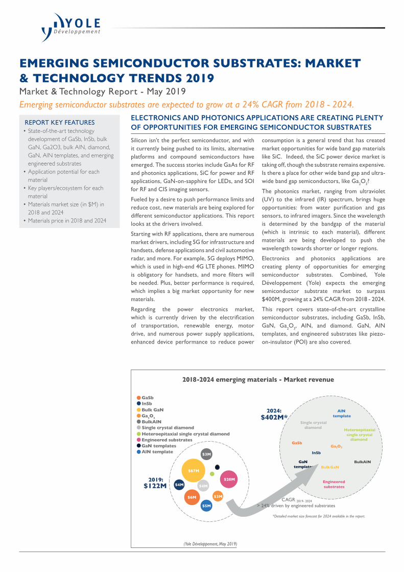
Electronics and photonics applications are creating plenty of opportunities for emerging semiconductor substrates. Combined, Yole Développement (Yole) expects the emerging semiconductor substrate market to surpass $400M, growing at a 24% CAGR from 2018 - 2024.
This report covers state-of-the-art crystalline semiconductor substrates, including GaSb, InSb, GaN, Ga
2O3, AlN, and diamond. GaN, AlN templates, and engineered substrates like piezo-on-insulator (POI) are also covered.
EMERGING SEMICONDUCTOR SUBSTRATES: MARKET & TECHNOLOGY TRENDS 2019Market & Technology Report - May 2019Emerging semiconductor substrates are expected to grow at a 24% CAGR from 2018 - 2024.
REPORT KEY FEATURES • State-of-the-art technology
development of GaSb, InSb, bulkGaN, Ga2O3, bulk AlN, diamond,GaN, AlN templates, and emergingengineered substrates
• Application potential for eachmaterial
• Key players/ecosystem for eachmaterial
• Materials market size (in $M) in2018 and 2024
• Materials price in 2018 and 2024
(Yole Développement, May 2019)
2018-2024 emerging materials - Market revenue
ELECTRONICS AND PHOTONICS APPLICATIONS ARE CREATING PLENTY OF OPPORTUNITIES FOR EMERGING SEMICONDUCTOR SUBSTRATES
$67M
2024: $402M*
2019:$122M
• GaSb• InSb• Bulk GaN• Ga2O3• BulkAlN • Single crystal diamond• Heteroepitaxial single crystal diamond• Engineered substrates• GaN templates• AlN template
$4M
$3M
$6M
$4M
$3M
$20M
$5M
*Detailed market size forecast for 2024 available in the report.
GaSb
InSb
Bulk GaN
Ga2O3
Bulk AlN
Single crystal diamond Heteroepitaxial
single crystal diamond
Engineered substrates
AlNtemplate
GaNtemplates
CAGR 2019- 2024
> 24% driven by engineered substrates
EMERGING SEMICONDUCTOR SUBSTRATES: MARKET & TECHNOLOGY TRENDS 2019
Researchers and engineers have plenty of ideas, and now the questions are, “Which emerging semiconductor substrate will be the next game-changer?” and “For which application”?
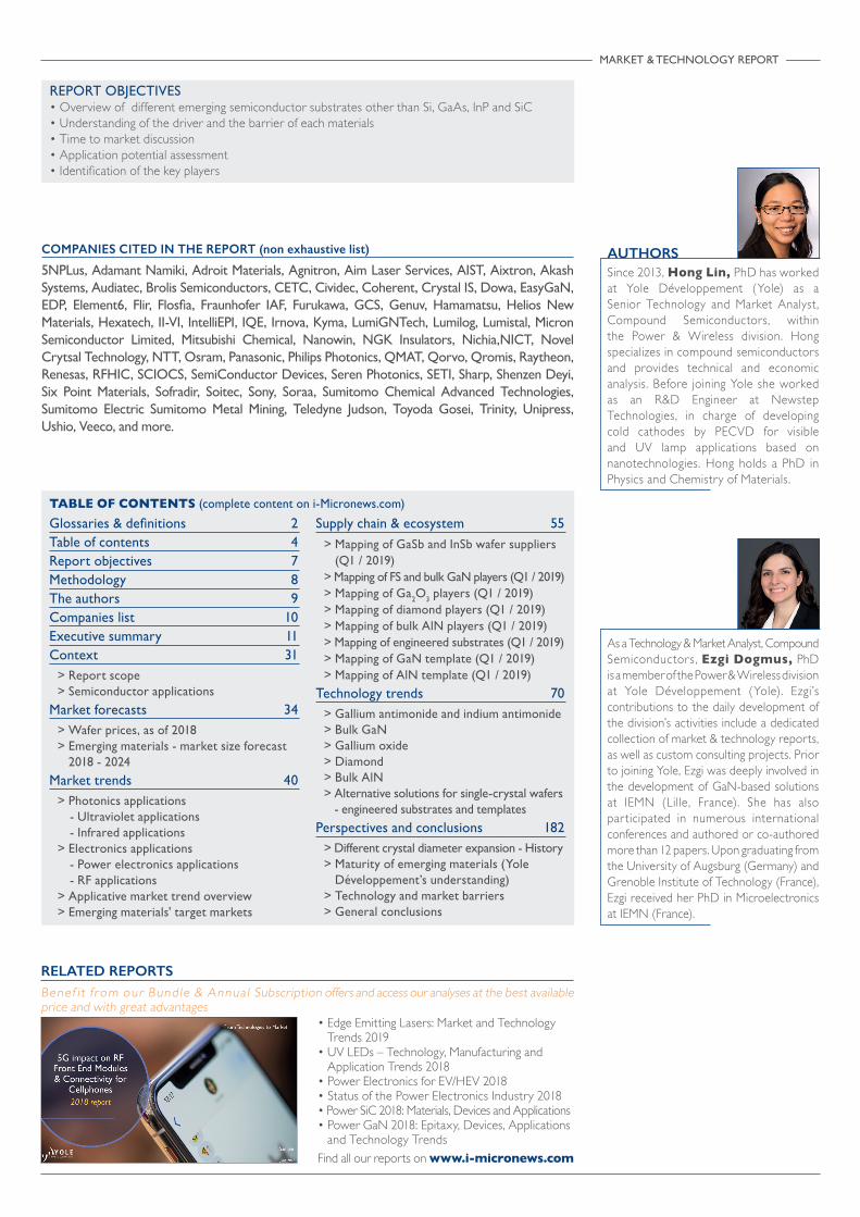
Starting with GaSb and InSb, laser diodes (LDs) and photodiodes (PDs) based on these materials are already deployed in performance-driven military applications. But this is not all. For example, IQE, a leading antimonide wafer and epiwafer supplier, is actively engaged with tier1 OEMs on new opportunities to migrate antimonide-based “see in the dark” IR technologies into consumer markets. Yole also sees that an emerging GaSb-based type-2-superlattice (T2SL) technology is being developed by several major detector players including FLIR, Semiconductor Devices, and IRnova. This technology is expected to penetrate into consumer applications, with ramp-up in the coming years.
Bulk GaN wafers have for many years been widely used for laser diode applications. Recently, researchers have explored their usage in power electronics and RF
applications. We see a growing effort, led by Japanese players (ranging from materials suppliers to device suppliers like Toyoda Gosei), to make vertical GaN-on-GaN power devices happen. In the meantime, an ultra-wide band gap material (Ga
2O3) is garnering increased attention. Wafers up to six inches have been demonstrated, with the promise of potentially lower cost than today’s SiC solutions. Future ramp-up will depend on technology/cost competition from other existing solutions.
Up to now we have considered bulk crystal materials, but they are not the whole story. Templates and engineered substrates are also being developed for either lower cost (i.e. SiC and poly SiC bonding) or better performance, such as piezo-on-insulator for filter applications.
This report conveys Yole understanding of these substrates’ application potential in RF, power electronics, photonics (including laser diodes), LEDs, sensors, and detectors.
THERE ARE MANY DRIVERS FOR EMERGING MATERIALS
(Yole Développement, May 2019)
GaSb
InSb
Both(GaSb & InSb)
IQE acquired Galaxy Semiconductor and Wafer technology
Mapping of other semiconductor substrates are available in the report. *non-exhausitve list of companies
Mapping of GaSb and InSb wafer suppliers* (Q1, 2019)
2018-2024 emerging materials' target markets
(Yole Développement, May 2019)
Diamond
LD LED LED Sensors/Detectors RF Power
• Automotive lighting
• Water, air disinfection, purification by UV LEDs
• Displays• Display systems
for VR/AR and MR
• Gas sensors• Infrared
imagers
• 5G for cell phone industry
• Solid stateradar for military applications
• Electric/Hybrid electric vehicles
• Renewable energies (wind, PV)
• T&D• Rail
Bulk GaN
InSb
GaSbDiamond
Ga2O3
Bulk GaN
Bulk GaN
AlN
Engineered substrates
GaNtemplate
Engineered substrates
AlNTemplate
Ga2O3
Bulk GaN
AlN
AlNTemplate
MARKET & TECHNOLOGY REPORT
COMPANIES CITED IN THE REPORT (non exhaustive list)
5NPLus, Adamant Namiki, Adroit Materials, Agnitron, Aim Laser Services, AIST, Aixtron, Akash Systems, Audiatec, Brolis Semiconductors, CETC, Cividec, Coherent, Crystal IS, Dowa, EasyGaN, EDP, Element6, Flir, Flosfia, Fraunhofer IAF, Furukawa, GCS, Genuv, Hamamatsu, Helios New Materials, Hexatech, II-VI, IntelliEPI, IQE, Irnova, Kyma, LumiGNTech, Lumilog, Lumistal, Micron Semiconductor Limited, Mitsubishi Chemical, Nanowin, NGK Insulators, Nichia,NICT, Novel Crytsal Technology, NTT, Osram, Panasonic, Philips Photonics, QMAT, Qorvo, Qromis, Raytheon, Renesas, RFHIC, SCIOCS, SemiConductor Devices, Seren Photonics, SETI, Sharp, Shenzen Deyi, Six Point Materials, Sofradir, Soitec, Sony, Soraa, Sumitomo Chemical Advanced Technologies, Sumitomo Electric Sumitomo Metal Mining, Teledyne Judson, Toyoda Gosei, Trinity, Unipress, Ushio, Veeco, and more.
RELATED REPORTSBenef i t f rom our Bundle & Annual Subscription offers and access our analyses at the best available price and with great advantages
• Edge Emitting Lasers: Market and Technology Trends 2019
• UV LEDs – Technology, Manufacturing and Application Trends 2018
• Power Electronics for EV/HEV 2018• Status of the Power Electronics Industry 2018• Power SiC 2018: Materials, Devices and Applications• Power GaN 2018: Epitaxy, Devices, Applications
and Technology TrendsFind all our reports on www.i-micronews.com
Since 2013, Hong Lin, PhD has worked at Yole Développement (Yole) as a Senior Technology and Market Analyst, Compound Semiconductors, within the Power & Wireless division. Hong specializes in compound semiconductors and provides technical and economic analysis. Before joining Yole she worked as an R&D Engineer at Newstep Technologies, in charge of developing cold cathodes by PECVD for visible and UV lamp applications based on nanotechnologies. Hong holds a PhD in Physics and Chemistry of Materials.
AUTHORS
TABLE OF CONTENTS (complete content on i-Micronews.com)
Glossaries & definitions 2Table of contents 4Report objectives 7Methodology 8The authors 9Companies list 10Executive summary 11Context 31
> Report scope > Semiconductor applications
Market forecasts 34> Wafer prices, as of 2018> Emerging materials - market size forecast
2018 - 2024Market trends 40
> Photonics applications- Ultraviolet applications- Infrared applications
> Electronics applications- Power electronics applications- RF applications
> Applicative market trend overview> Emerging materials' target markets
Supply chain & ecosystem 55> Mapping of GaSb and InSb wafer suppliers
(Q1 / 2019)> Mapping of FS and bulk GaN players (Q1 / 2019) > Mapping of Ga2O3 players (Q1 / 2019) > Mapping of diamond players (Q1 / 2019) > Mapping of bulk AlN players (Q1 / 2019) > Mapping of engineered substrates (Q1 / 2019) > Mapping of GaN template (Q1 / 2019) > Mapping of AlN template (Q1 / 2019)
Technology trends 70> Gallium antimonide and indium antimonide> Bulk GaN > Gallium oxide> Diamond> Bulk AlN> Alternative solutions for single-crystal wafers
- engineered substrates and templatesPerspectives and conclusions 182
> Different crystal diameter expansion - History> Maturity of emerging materials (Yole
Développement’s understanding)> Technology and market barriers> General conclusions
REPORT OBJECTIVES• Overview of different emerging semiconductor substrates other than Si, GaAs, InP and SiC• Understanding of the driver and the barrier of each materials• Time to market discussion• Application potential assessment• Identification of the key players
As a Technology & Market Analyst, Compound Semiconductors, Ezgi Dogmus, PhD is a member of the Power & Wireless division at Yole Développement (Yole). Ezgi’s contributions to the daily development of the division’s activities include a dedicated collection of market & technology reports, as well as custom consulting projects. Prior to joining Yole, Ezgi was deeply involved in the development of GaN-based solutions at IEMN (Lille, France). She has also par ticipated in numerous international conferences and authored or co-authored more than 12 papers. Upon graduating from the University of Augsburg (Germany) and Grenoble Institute of Technology (France), Ezgi received her PhD in Microelectronics at IEMN (France).
ORDER FORMEmerging Semiconductor Substrates: Market & Technology Trends 2019
SHIPPING CONTACT
First Name:
Email:
Last Name:
Phone:
PAYMENT
BY CREDIT CARD Visa Mastercard Amex
Name of the Card Holder:
Credit Card Number:
Card Verification Value (3 digits except AMEX: 4 digits): Expiration date:
BY BANK TRANSFERBANK INFO: HSBC, 1 place de la Bourse, F-69002 Lyon, France, Bank code: 30056, Branch code: 00170Account No: 0170 200 1565 87, SWIFT or BIC code: CCFRFRPP, IBAN: FR76 3005 6001 7001 7020 0156 587
RETURN ORDER BY • MAIL: YOLE DÉVELOPPEMENT, Le Quartz,
75 Cours Emile Zola, 69100 Villeurbanne/Lyon - France
SALES CONTACTS • Western US & Canada - Steve Laferriere:
+ 1 310 600-8267 – [email protected]• Eastern US & Canada - Chris Youman:
+1 919 607 9839 – [email protected]• Europe & RoW - Lizzie Levenez:
+ 49 15 123 544 182 – [email protected]• Japan & Rest of Asia - Takashi Onozawa:
+81-80-4371-4887 – [email protected]• Greater China - Mavis Wang:
+886 979 336 809 – [email protected]• Korea - Peter OK: +82 10 4089 0233 – [email protected]• Specific inquiries: +33 472 830 180 – [email protected](1) Our Terms and Conditions of Sale are available at
www.yole.fr/Terms_and_Conditions_of_Sale.aspx The present document is valid 24 months after its publishing date: May 23, 2019
/
ABOUT YOLE DEVELOPPEMENT
BILL TO
Name (Mr/Ms/Dr/Pr):
Job Title:
Company:
Address:
City:
State:
Postcode/Zip:
Country*:
*VAT ID Number for EU members:
Tel:
Email:
Date:
PRODUCT ORDER - Ref YD19019Please enter my order for above named report: One user license*: Euro 5,990 Multi user license: Euro 6,490- The report will be ready for delivery from May 23, 2019- For price in dollars, please use the day’s exchange rate. All reports are
delivered electronically at payment reception. For French customers, add 20% for VAT
I hereby accept Yole Développement’s Terms and Conditions of Sale(1)
Signature:
*One user license means only one person at the company can use the report.
Founded in 1998, Yole Développement has grown to become a group of companies providing marketing, technology and strategy consulting, media and corporate finance services, reverse engineering and reverse costing services and well as IP and patent analysis. With a strong focus on emerging applications using silicon and/or micro manufacturing, the Yole group of companies has expanded to include more than 80 collaborators worldwide covering MEMS and Image Sensors, Compound Semiconductors, RF Electronics, Solid-State Lighting, Displays, Software, Optoelectronics, Microfluidics & Medical, Advanced Packaging, Manufacturing, Nanomaterials, Power Electronics and Batteries & Energy Management.The “More than Moore” market research, technology and strategy consulting company Yole Développement, along with its partners System Plus Consulting, PISEO and KnowMade, support industrial companies, investors and R&D organizations worldwide to help them understand markets and follow technology trends to grow their business.
CONSULTING AND ANALYSIS• Market data & research, marketing analysis• Technology analysis• Strategy consulting• Reverse engineering & costing• Patent analysis• Design and characterization of innovative optical systems• Financial services (due diligence, M&A with our partner)More information on www.yole.fr
MEDIA & EVENTS• i-Micronews.com website & related e-newsletter• Communication & webcast services• Events: TechDays, forums…More information on www.i-Micronews.com
REPORTS• Market & technology reports• Patent investigation and patent infringement risk analysis• Structure, process and cost analysis• Cost simulation toolMore information on www.i-micronews.com/reports
CONTACTSFor more information about :• Consulting & Financial Services: Jean-Christophe Eloy ([email protected])• Reports: David Jourdan ([email protected]) Yole Group of Companies• Press Relations & Corporate Communication: Sandrine Leroy ([email protected])
© 2019
Yole Développement
From Technologies to Market
Source: Wikimedia Commons
21©2019 | www.yole.fr | About Yole Développement
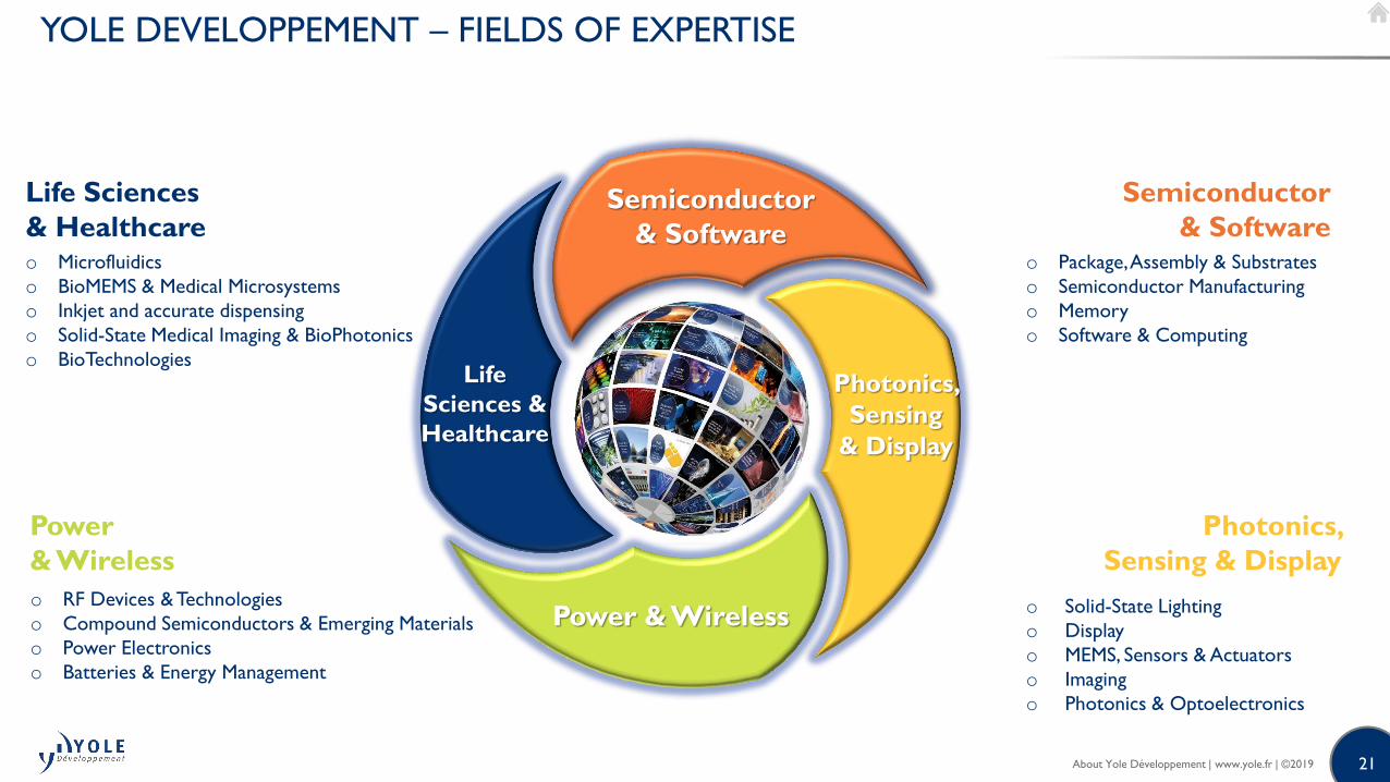
YOLE DEVELOPPEMENT – FIELDS OF EXPERTISE
Life Sciences
& Healthcare o Microfluidics
o BioMEMS & Medical Microsystems
o Inkjet and accurate dispensing
o Solid-State Medical Imaging & BioPhotonics
o BioTechnologies
Power
& Wireless
o RF Devices & Technologies
o Compound Semiconductors & Emerging Materials
o Power Electronics
o Batteries & Energy Management
Semiconductor
& Software o Package,Assembly & Substrates
o Semiconductor Manufacturing
o Memory
o Software & Computing
Photonics,
Sensing & Display
o Solid-State Lighting
o Display
o MEMS, Sensors & Actuators
o Imaging
o Photonics & Optoelectronics
Semiconductor
& Software
Power & Wireless
Photonics,
Sensing
& Display
Life
Sciences &
Healthcare
About Yole Développement | www.yole.fr | ©2019
22©2019 | www.yole.fr | About Yole Développement
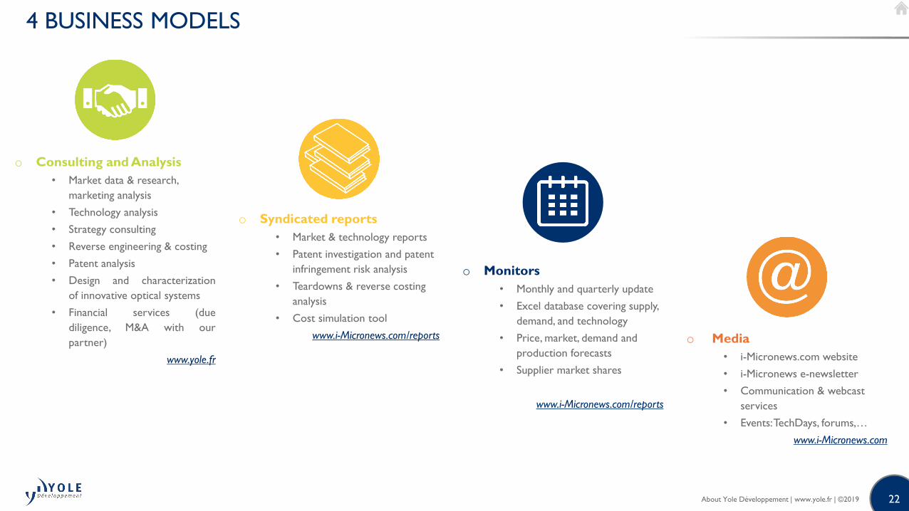
4 BUSINESS MODELS
o Consulting and Analysis
• Market data & research,
marketing analysis
• Technology analysis
• Strategy consulting
• Reverse engineering & costing
• Patent analysis
• Design and characterization
of innovative optical systems
• Financial services (due
diligence, M&A with our
partner)
www.yole.fr
o Syndicated reports
• Market & technology reports
• Patent investigation and patent
infringement risk analysis
• Teardowns & reverse costing
analysis
• Cost simulation tool
www.i-Micronews.com/reports o Media
• i-Micronews.com website
• i-Micronews e-newsletter
• Communication & webcast
services
• Events: TechDays, forums,…
www.i-Micronews.com
o Monitors
• Monthly and quarterly update
• Excel database covering supply,
demand, and technology
• Price, market, demand and
production forecasts
• Supplier market shares
www.i-Micronews.com/reports
About Yole Développement | www.yole.fr | ©2019
23©2019 | www.yole.fr | About Yole Développement
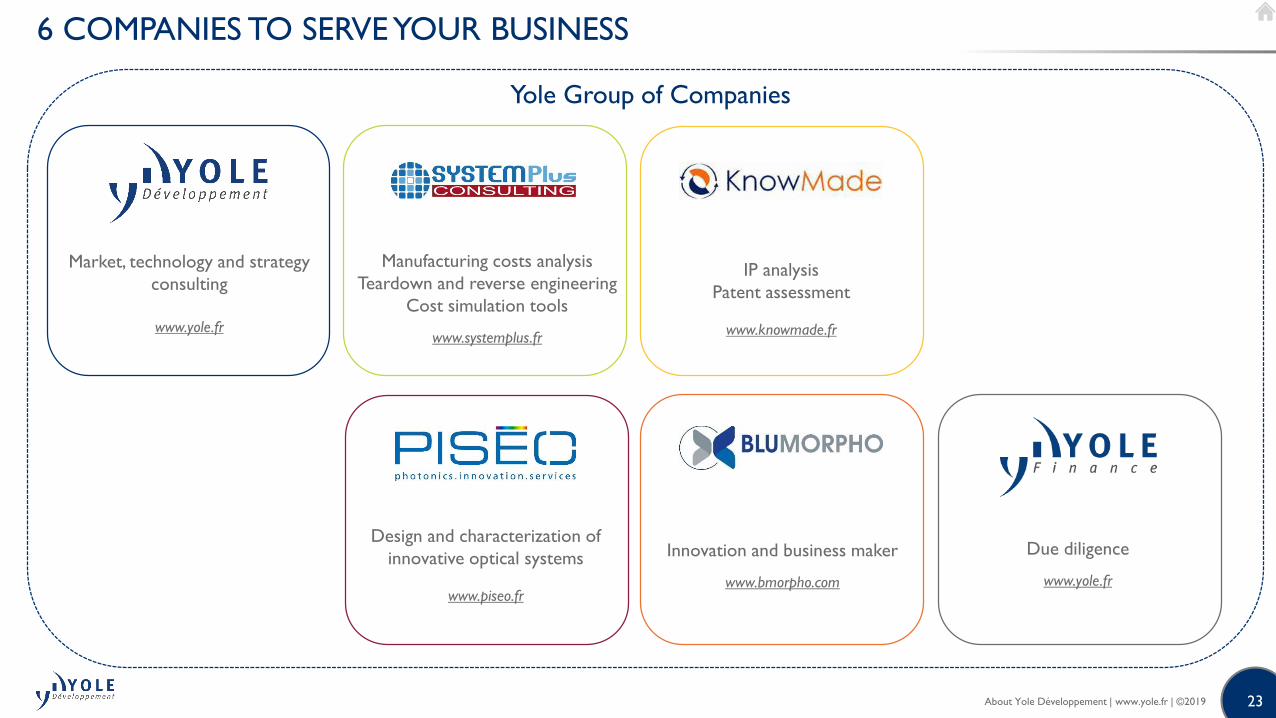
6 COMPANIES TO SERVE YOUR BUSINESS
Due diligence
www.yole.fr
Manufacturing costs analysis
Teardown and reverse engineering
Cost simulation tools
www.systemplus.fr
Market, technology and strategy
consulting
www.yole.fr
IP analysis
Patent assessment
www.knowmade.fr
Innovation and business maker
www.bmorpho.com
Design and characterization of
innovative optical systems
www.piseo.fr
Yole Group of Companies
About Yole Développement | www.yole.fr | ©2019
24
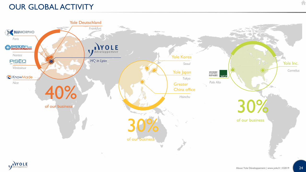
OUR GLOBAL ACTIVITY
30%of our business
40%of our business 30%
of our business
Greater
China office
Yole Japan
HQ in Lyon
Nantes
Paris
Nice
Vénissieux
Yole Deutschland
Frankfurt
Hsinchu
Tokyo
Yole Korea
Seoul
Palo Alto
Yole Inc.
Cornelius
About Yole Développement | www.yole.fr | ©2019

25©2019 | www.yole.fr | About Yole Développement
ANALYSIS SERVICES - CONTENT COMPARISON
High
Technology
and Market
Report
Leadership
Meeting
Q&A
Service
Depth of the analysis
Bre
adth
of th
e a
nal
ysis
Meet the
Analyst
Custom
Analysis
High
Low
About Yole Développement | www.yole.fr | ©2019
26©2019 | www.yole.fr | About Yole Développement
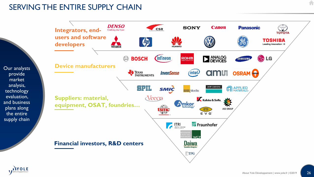
SERVING THE ENTIRE SUPPLY CHAIN
Our analysts provide market analysis,
technology evaluation,
and business plans along the entire
supply chain
Integrators, end-
users and software
developers
Device manufacturers
Suppliers: material,
equipment, OSAT, foundries…
Financial investors, R&D centers
About Yole Développement | www.yole.fr | ©2019

27©2019 | www.yole.fr | About Yole Développement
SERVING MULTIPLE INDUSTRIAL FIELDS
We workacross
multiples industries to understand
the impact of More-than-
Moore technologies from deviceto system
From A to Z…
Transportation
makers
Mobile phone
and
consumer
electronics
Automotive
Medical
systems
Industrial
and defense
Energy
management
About Yole Développement | www.yole.fr | ©2019

28
o Over the course of more than 20 years, Yole Développement has grown to become a group of companies. Together with System Plus Consulting and KnowMade, we now
provide marketing, technology and strategy consulting, media and corporate finance services, reverse costing, structure, process and cost analysis services and well as
intellectual property (IP) and patent analysis. Together, our group of companies is collaborating ever closer and therefore will offer, in 2019, a collection of over 125 reports,
10 new monitors and 120 teardowns. Combining respective expertise and methodologies from the three companies, they cover:
o If you are looking for:
• An analysis of your product market and technology
• A review of how your competitors are evolving
• An understanding of your manufacturing and production costs
• An understanding of your industry’s technology roadmap and related IPs
• A clear view supply chain evolution
Our reports and monitors are for you!
o Our team of over 70 analysts, including PhD and MBA qualified industry veterans from Yole Développement, System Plus Consulting and KnowMade, collect information,identify trends, challenges, emerging markets, and competitive environments. They turn that information into results and give you a complete picture of your industry’slandscape. In the past 20 years, we have worked on more than 2,000 projects, interacting with technology professionals and high-level opinion makers from the mainplayers of their industries and realized more than 5,000 interviews per year.
WHAT TO EXPECT IN 2019?In 2019 we will extend our offering with a new ‘monitor’ product which provides more updates on your industry during the year. The Yole Group of Companies is also buildingon and expanding its investigations of the memory industry. Moreover, in parallel, the Yole Group reaffirms its commitment to a new collection of reports mixing software andhardware and is increasing its involvement in displays, radio-frequency (RF) technology, advanced substrates, batteries and compound semiconductors. Last but not least,System Plus Consulting is developing its teardowns service providing 120+ offers related to phones, smart home, wearables and connected devices. Discover our 2019program right now, and ensure you get a true vision of the industry. Stay tuned!
REPORTS COLLECTION
www.i-Micronews.com
• MEMS & Sensors
• RF devices & technologies
• Medical technologies
• Semiconductor Manufacturing
• Advanced packaging
• Memory
• Batteries and energy management
• Power electronics
• Compound semiconductors
• Solid state lighting
• Displays
• Software
• Imaging
• Photonics
About Yole Développement | www.yole.fr | ©2019
29
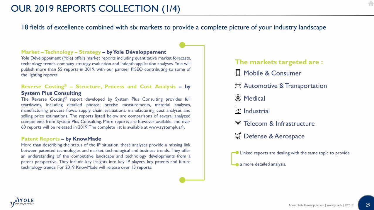
OUR 2019 REPORTS COLLECTION (1/4)
18 fields of excellence combined with six markets to provide a complete picture of your industry landscape
Market –Technology – Strategy – by Yole DéveloppementYole Développement (Yole) offers market reports including quantitative market forecasts,
technology trends, company strategy evaluation and indepth application analyses. Yole will
publish more than 55 reports in 2019, with our partner PISEO contributing to some of
the lighting reports.
Reverse Costing® – Structure, Process and Cost Analysis – by
System Plus ConsultingThe Reverse Costing® report developed by System Plus Consulting provides full
teardowns, including detailed photos, precise measurements, material analyses,
manufacturing process flows, supply chain evaluations, manufacturing cost analyses and
selling price estimations. The reports listed below are comparisons of several analyzed
components from System Plus Consulting. More reports are however available, and over
60 reports will be released in 2019.The complete list is available at www.systemplus.fr.
Patent Reports – by KnowMadeMore than describing the status of the IP situation, these analyses provide a missing link
between patented technologies and market, technological and business trends. They offer
an understanding of the competitive landscape and technology developments from a
patent perspective. They include key insights into key IP players, key patents and future
technology trends. For 2019 KnowMade will release over 15 reports.
The markets targeted are :
• Mobile & Consumer
• Automotive & Transportation
• Medical
• Industrial
• Telecom & Infrastructure
• Defense & Aerospace
• Linked reports are dealing with the same topic to provide
• a more detailed analysis.
About Yole Développement | www.yole.fr | ©2019
30
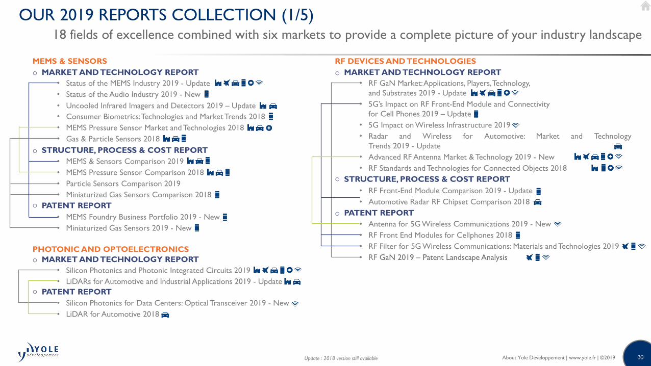
OUR 2019 REPORTS COLLECTION (1/5)18 fields of excellence combined with six markets to provide a complete picture of your industry landscape
MEMS & SENSORS
o MARKET AND TECHNOLOGY REPORT
• Status of the MEMS Industry 2019 - Update
• Status of the Audio Industry 2019 - New
• Uncooled Infrared Imagers and Detectors 2019 – Update
• Consumer Biometrics:Technologies and Market Trends 2018
• MEMS Pressure Sensor Market and Technologies 2018
• Gas & Particle Sensors 2018
o STRUCTURE, PROCESS & COST REPORT
• MEMS & Sensors Comparison 2019
• MEMS Pressure Sensor Comparison 2018
• Particle Sensors Comparison 2019
• Miniaturized Gas Sensors Comparison 2018
o PATENT REPORT
• MEMS Foundry Business Portfolio 2019 - New
• Miniaturized Gas Sensors 2019 - New
PHOTONIC AND OPTOELECTRONICS
o MARKET ANDTECHNOLOGY REPORT
• Silicon Photonics and Photonic Integrated Circuits 2019
• LiDARs for Automotive and Industrial Applications 2019 - Update
o PATENT REPORT
• Silicon Photonics for Data Centers: Optical Transceiver 2019 - New
• LiDAR for Automotive 2018
RF DEVICES AND TECHNOLOGIES
o MARKET ANDTECHNOLOGY REPORT
• RF GaN Market: Applications, Players, Technology,
and Substrates 2019 - Update
• 5G’s Impact on RF Front-End Module and Connectivity
for Cell Phones 2019 – Update
• 5G Impact on Wireless Infrastructure 2019
• Radar and Wireless for Automotive: Market and Technology
Trends 2019 - Update
• Advanced RF Antenna Market & Technology 2019 - New
• RF Standards and Technologies for Connected Objects 2018
o STRUCTURE, PROCESS & COST REPORT
• RF Front-End Module Comparison 2019 - Update
• Automotive Radar RF Chipset Comparison 2018
o PATENT REPORT
• Antenna for 5G Wireless Communications 2019 - New
• RF Front End Modules for Cellphones 2018
• RF Filter for 5G Wireless Communications: Materials and Technologies 2019
• RF GaN 2019 – Patent Landscape Analysis
Update : 2018 version still available About Yole Développement | www.yole.fr | ©2019
31
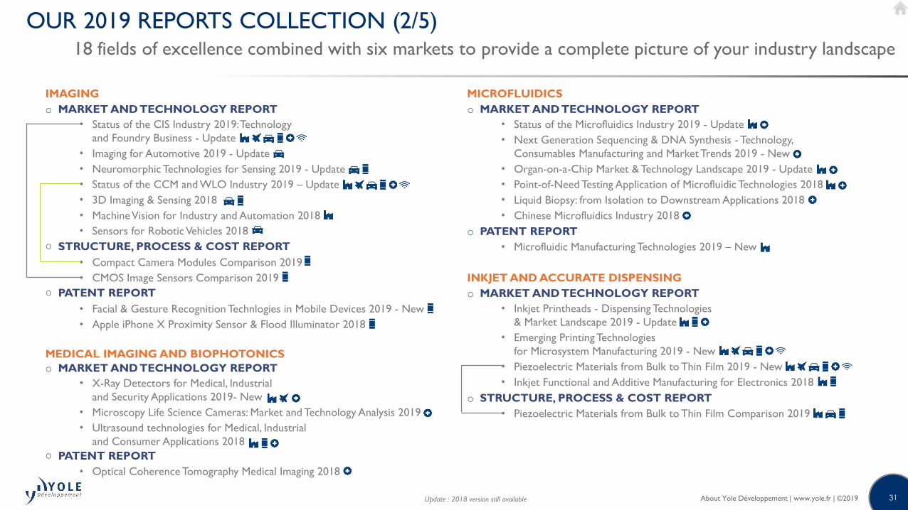
OUR 2019 REPORTS COLLECTION (2/5)18 fields of excellence combined with six markets to provide a complete picture of your industry landscape
IMAGING
o MARKET AND TECHNOLOGY REPORT
• Status of the CIS Industry 2019: Technology
and Foundry Business - Update
• Imaging for Automotive 2019 - Update
• Neuromorphic Technologies for Sensing 2019 - Update
• Status of the CCM and WLO Industry 2019 – Update
• 3D Imaging & Sensing 2018
• MachineVision for Industry and Automation 2018
• Sensors for Robotic Vehicles 2018
o STRUCTURE, PROCESS & COST REPORT
• Compact Camera Modules Comparison 2019
• CMOS Image Sensors Comparison 2019
o PATENT REPORT
• Facial & Gesture Recognition Technlogies in Mobile Devices 2019 - New
• Apple iPhone X Proximity Sensor & Flood Illuminator 2018
MEDICAL IMAGING AND BIOPHOTONICS
o MARKET ANDTECHNOLOGY REPORT
• X-Ray Detectors for Medical, Industrial
and Security Applications 2019- New
• Microscopy Life Science Cameras: Market and Technology Analysis 2019
• Ultrasound technologies for Medical, Industrial
and Consumer Applications 2018
o PATENT REPORT
• Optical Coherence Tomography Medical Imaging 2018
MICROFLUIDICS
o MARKET ANDTECHNOLOGY REPORT
• Status of the Microfluidics Industry 2019 - Update
• Next Generation Sequencing & DNA Synthesis - Technology,
Consumables Manufacturing and Market Trends 2019 - New
• Organ-on-a-Chip Market & Technology Landscape 2019 - Update
• Point-of-Need Testing Application of Microfluidic Technologies 2018
• Liquid Biopsy: from Isolation to Downstream Applications 2018
• Chinese Microfluidics Industry 2018
o PATENT REPORT
• Microfluidic Manufacturing Technologies 2019 – New
INKJET AND ACCURATE DISPENSING
o MARKET ANDTECHNOLOGY REPORT
• Inkjet Printheads - Dispensing Technologies
& Market Landscape 2019 - Update
• Emerging Printing Technologies
for Microsystem Manufacturing 2019 - New
• Piezoelectric Materials from Bulk to Thin Film 2019 - New
• Inkjet Functional and Additive Manufacturing for Electronics 2018
o STRUCTURE, PROCESS & COST REPORT
• Piezoelectric Materials from Bulk to Thin Film Comparison 2019
Update : 2018 version still available About Yole Développement | www.yole.fr | ©2019
32
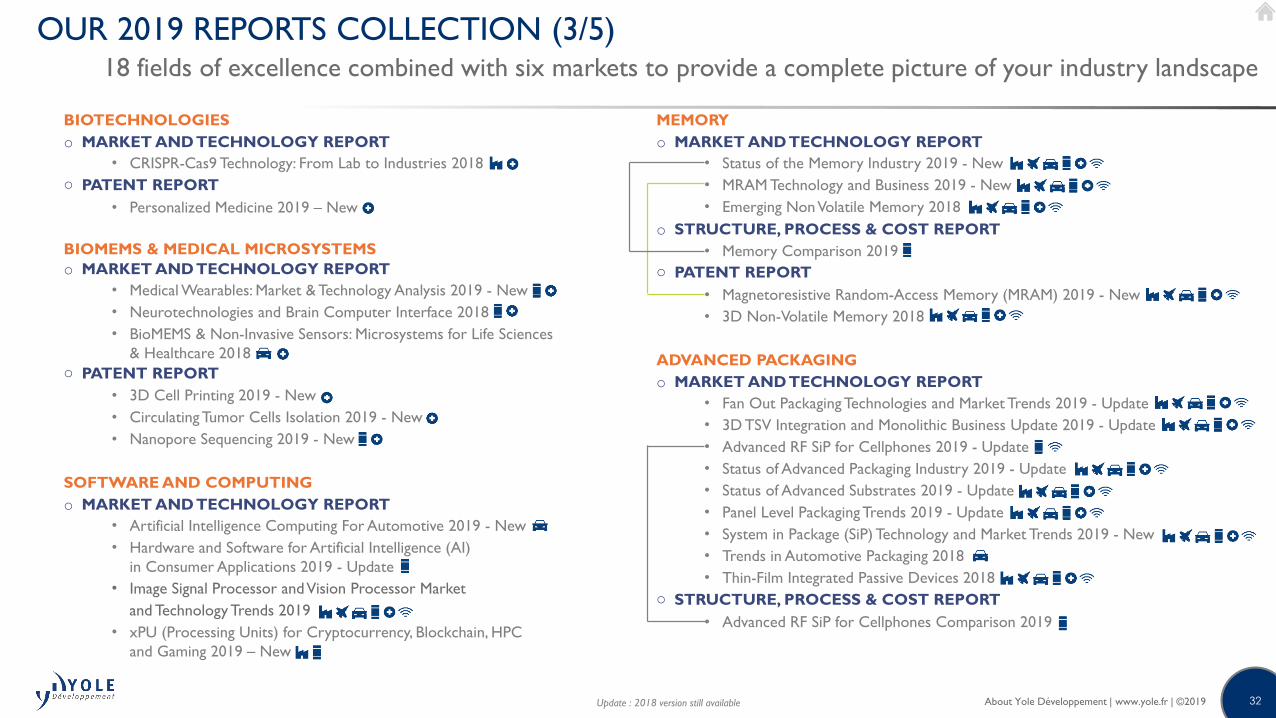
OUR 2019 REPORTS COLLECTION (3/5)18 fields of excellence combined with six markets to provide a complete picture of your industry landscape
BIOTECHNOLOGIES
o MARKET AND TECHNOLOGY REPORT
• CRISPR-Cas9 Technology: From Lab to Industries 2018
o PATENT REPORT
• Personalized Medicine 2019 – New
BIOMEMS & MEDICAL MICROSYSTEMS
o MARKET ANDTECHNOLOGY REPORT
• Medical Wearables: Market & Technology Analysis 2019 - New
• Neurotechnologies and Brain Computer Interface 2018
• BioMEMS & Non-Invasive Sensors: Microsystems for Life Sciences
& Healthcare 2018
o PATENT REPORT
• 3D Cell Printing 2019 - New
• Circulating Tumor Cells Isolation 2019 - New
• Nanopore Sequencing 2019 - New
SOFTWARE AND COMPUTING
o MARKET ANDTECHNOLOGY REPORT
• Artificial Intelligence Computing For Automotive 2019 - New
• Hardware and Software for Artificial Intelligence (AI)
in Consumer Applications 2019 - Update
• Image Signal Processor and Vision Processor Market
and Technology Trends 2019
• xPU (Processing Units) for Cryptocurrency, Blockchain, HPC
and Gaming 2019 – New
MEMORY
o MARKET AND TECHNOLOGY REPORT
• Status of the Memory Industry 2019 - New
• MRAM Technology and Business 2019 - New
• Emerging NonVolatile Memory 2018
o STRUCTURE, PROCESS & COST REPORT
• Memory Comparison 2019
o PATENT REPORT
• Magnetoresistive Random-Access Memory (MRAM) 2019 - New
• 3D Non-Volatile Memory 2018
ADVANCED PACKAGING
o MARKET ANDTECHNOLOGY REPORT
• Fan Out Packaging Technologies and Market Trends 2019 - Update
• 3D TSV Integration and Monolithic Business Update 2019 - Update
• Advanced RF SiP for Cellphones 2019 - Update
• Status of Advanced Packaging Industry 2019 - Update
• Status of Advanced Substrates 2019 - Update
• Panel Level Packaging Trends 2019 - Update
• System in Package (SiP) Technology and Market Trends 2019 - New
• Trends in Automotive Packaging 2018
• Thin-Film Integrated Passive Devices 2018
o STRUCTURE, PROCESS & COST REPORT
• Advanced RF SiP for Cellphones Comparison 2019
Update : 2018 version still available About Yole Développement | www.yole.fr | ©2019
33
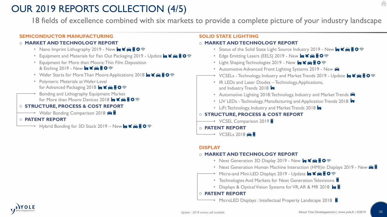
OUR 2019 REPORTS COLLECTION (4/5)18 fields of excellence combined with six markets to provide a complete picture of your industry landscape
SEMICONDUCTOR MANUFACTURING
o MARKET ANDTECHNOLOGY REPORT
• Nano Imprint Lithography 2019 - New
• Equipment and Materials for Fan Out Packaging 2019 - Update
• Equipment for More than Moore: Thin Film Deposition
& Etching 2019 - New
• Wafer Starts for More Than Moore Applications 2018
• Polymeric Materials at Wafer-Level
for Advanced Packaging 2018
• Bonding and Lithography Equipment Market
for More than Moore Devices 2018
o STRUCTURE, PROCESS & COST REPORT
• Wafer Bonding Comparison 2018
o PATENT REPORT
• Hybrid Bonding for 3D Stack 2019 – New
SOLID STATE LIGHTING
o MARKET ANDTECHNOLOGY REPORT
• Status of the Solid State Light Source Industry 2019 - New
• Edge Emitting Lasers (EELS) 2019 - New
• Light Shaping Technologies 2019 - New
• Automotive Advanced Front Lighting Systems 2019 - New
• VCSELs - Technology, Industry and Market Trends 2019 - Update
• IR LEDs and Laser Diodes – Technology, Applications,
and Industry Trends 2018
• Automotive Lighting 2018: Technology, Industry and Market Trends
• UV LEDs - Technology, Manufacturing and Application Trends 2018
• LiFi: Technology, Industry and Market Trends 2018
o STRUCTURE, PROCESS & COST REPORT
• VCSEL Comparison 2019
o PATENT REPORT
• VCSELs 2018
DISPLAY
o MARKET ANDTECHNOLOGY REPORT
• Next Generation 3D Display 2019 - New
• Next Generation Human Machine Interaction (HMI)in Displays 2019 - New
• Micro-and Mini-LED Displays 2019 - Update
• Technologies And Markets for Next Generation Televisions
• Displays & Optical Vision Systems for VR, AR & MR 2018
o PATENT REPORT
• MicroLED Displays : Intellectual Property Landscape 2018
Update : 2018 version still available About Yole Développement | www.yole.fr | ©2019
34
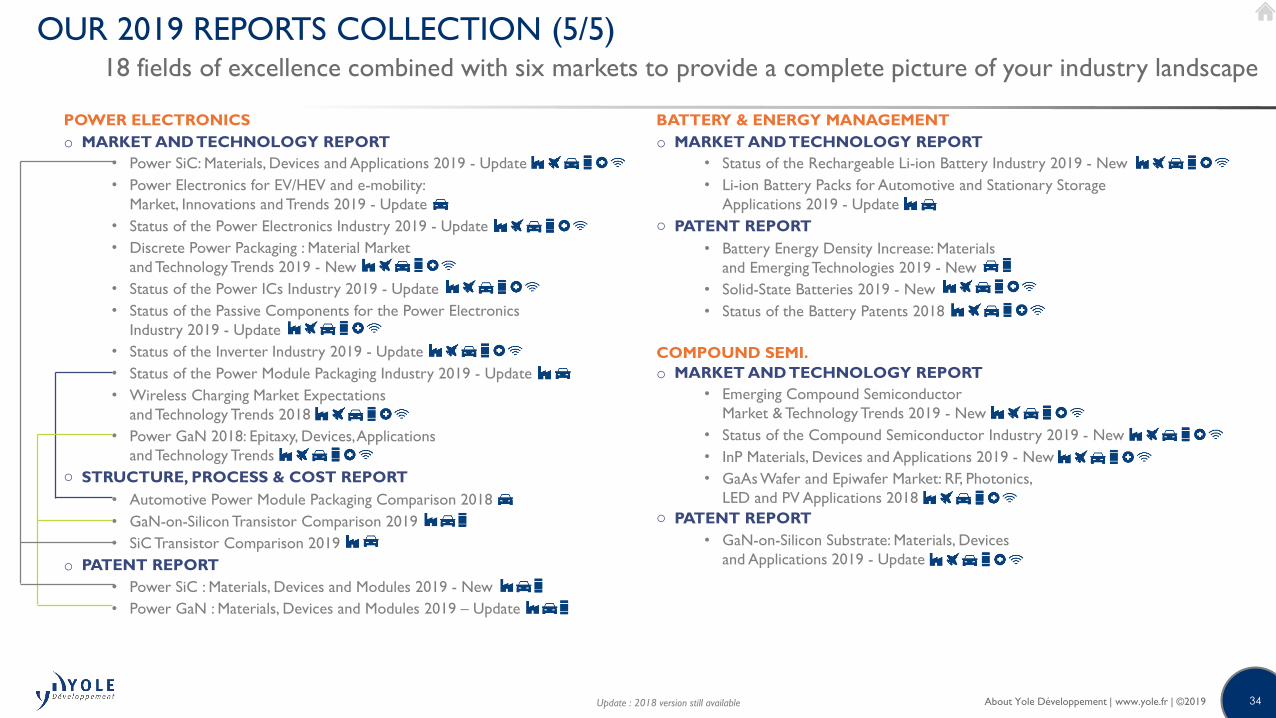
OUR 2019 REPORTS COLLECTION (5/5)18 fields of excellence combined with six markets to provide a complete picture of your industry landscape
POWER ELECTRONICS
o MARKET ANDTECHNOLOGY REPORT
• Power SiC: Materials, Devices and Applications 2019 - Update
• Power Electronics for EV/HEV and e-mobility:
Market, Innovations and Trends 2019 - Update
• Status of the Power Electronics Industry 2019 - Update
• Discrete Power Packaging : Material Market
and Technology Trends 2019 - New
• Status of the Power ICs Industry 2019 - Update
• Status of the Passive Components for the Power Electronics
Industry 2019 - Update
• Status of the Inverter Industry 2019 - Update
• Status of the Power Module Packaging Industry 2019 - Update
• Wireless Charging Market Expectations
and Technology Trends 2018
• Power GaN 2018: Epitaxy, Devices, Applications
and Technology Trends
o STRUCTURE, PROCESS & COST REPORT
• Automotive Power Module Packaging Comparison 2018
• GaN-on-Silicon Transistor Comparison 2019
• SiC Transistor Comparison 2019
o PATENT REPORT
• Power SiC : Materials, Devices and Modules 2019 - New
• Power GaN : Materials, Devices and Modules 2019 – Update
BATTERY & ENERGY MANAGEMENT
o MARKET ANDTECHNOLOGY REPORT
• Status of the Rechargeable Li-ion Battery Industry 2019 - New
• Li-ion Battery Packs for Automotive and Stationary Storage
Applications 2019 - Update
o PATENT REPORT
• Battery Energy Density Increase: Materials
and Emerging Technologies 2019 - New
• Solid-State Batteries 2019 - New
• Status of the Battery Patents 2018
COMPOUND SEMI.
o MARKET ANDTECHNOLOGY REPORT
• Emerging Compound Semiconductor
Market & Technology Trends 2019 - New
• Status of the Compound Semiconductor Industry 2019 - New
• InP Materials, Devices and Applications 2019 - New
• GaAs Wafer and Epiwafer Market: RF, Photonics,
LED and PV Applications 2018
o PATENT REPORT
• GaN-on-Silicon Substrate: Materials, Devices
and Applications 2019 - Update
Update : 2018 version still available About Yole Développement | www.yole.fr | ©2019
35
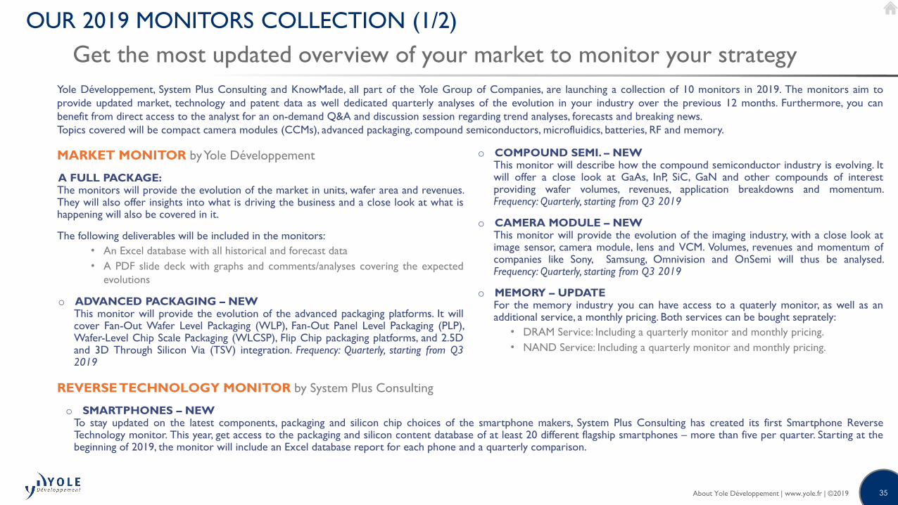
OUR 2019 MONITORS COLLECTION (1/2)
Get the most updated overview of your market to monitor your strategy
Yole Développement, System Plus Consulting and KnowMade, all part of the Yole Group of Companies, are launching a collection of 10 monitors in 2019. The monitors aim to
provide updated market, technology and patent data as well dedicated quarterly analyses of the evolution in your industry over the previous 12 months. Furthermore, you can
benefit from direct access to the analyst for an on-demand Q&A and discussion session regarding trend analyses, forecasts and breaking news.
Topics covered will be compact camera modules (CCMs), advanced packaging, compound semiconductors, microfluidics, batteries, RF and memory.
MARKET MONITOR byYole Développement
A FULL PACKAGE:The monitors will provide the evolution of the market in units, wafer area and revenues.They will also offer insights into what is driving the business and a close look at what ishappening will also be covered in it.
The following deliverables will be included in the monitors:
• An Excel database with all historical and forecast data
• A PDF slide deck with graphs and comments/analyses covering the expected
evolutions
o ADVANCED PACKAGING – NEWThis monitor will provide the evolution of the advanced packaging platforms. It willcover Fan-Out Wafer Level Packaging (WLP), Fan-Out Panel Level Packaging (PLP),Wafer-Level Chip Scale Packaging (WLCSP), Flip Chip packaging platforms, and 2.5Dand 3D Through Silicon Via (TSV) integration. Frequency: Quarterly, starting from Q32019
o COMPOUND SEMI. – NEWThis monitor will describe how the compound semiconductor industry is evolving. Itwill offer a close look at GaAs, InP, SiC, GaN and other compounds of interestproviding wafer volumes, revenues, application breakdowns and momentum.Frequency: Quarterly, starting from Q3 2019
o CAMERA MODULE – NEWThis monitor will provide the evolution of the imaging industry, with a close look atimage sensor, camera module, lens and VCM. Volumes, revenues and momentum ofcompanies like Sony, Samsung, Omnivision and OnSemi will thus be analysed.Frequency: Quarterly, starting from Q3 2019
o MEMORY – UPDATEFor the memory industry you can have access to a quaterly monitor, as well as anadditional service, a monthly pricing. Both services can be bought seprately:
• DRAM Service: Including a quarterly monitor and monthly pricing.
• NAND Service: Including a quarterly monitor and monthly pricing.
REVERSETECHNOLOGY MONITOR by System Plus Consulting
o SMARTPHONES – NEWTo stay updated on the latest components, packaging and silicon chip choices of the smartphone makers, System Plus Consulting has created its first Smartphone ReverseTechnology monitor. This year, get access to the packaging and silicon content database of at least 20 different flagship smartphones – more than five per quarter. Starting at thebeginning of 2019, the monitor will include an Excel database report for each phone and a quarterly comparison.
About Yole Développement | www.yole.fr | ©2019
36
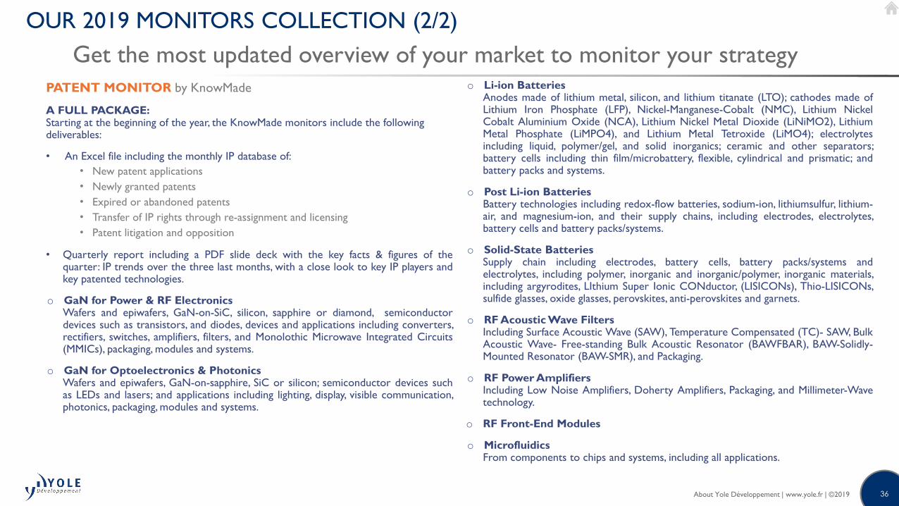
OUR 2019 MONITORS COLLECTION (2/2)
Get the most updated overview of your market to monitor your strategy
PATENT MONITOR by KnowMade
A FULL PACKAGE:Starting at the beginning of the year, the KnowMade monitors include the following deliverables:
• An Excel file including the monthly IP database of:
• New patent applications
• Newly granted patents
• Expired or abandoned patents
• Transfer of IP rights through re-assignment and licensing
• Patent litigation and opposition
• Quarterly report including a PDF slide deck with the key facts & figures of thequarter: IP trends over the three last months, with a close look to key IP players andkey patented technologies.
o GaN for Power & RF ElectronicsWafers and epiwafers, GaN-on-SiC, silicon, sapphire or diamond, semiconductordevices such as transistors, and diodes, devices and applications including converters,rectifiers, switches, amplifiers, filters, and Monolothic Microwave Integrated Circuits(MMICs), packaging, modules and systems.
o GaN for Optoelectronics & PhotonicsWafers and epiwafers, GaN-on-sapphire, SiC or silicon; semiconductor devices suchas LEDs and lasers; and applications including lighting, display, visible communication,photonics, packaging, modules and systems.
o Li-ion BatteriesAnodes made of lithium metal, silicon, and lithium titanate (LTO); cathodes made ofLithium Iron Phosphate (LFP), Nickel-Manganese-Cobalt (NMC), Lithium NickelCobalt Aluminium Oxide (NCA), Lithium Nickel Metal Dioxide (LiNiMO2), LithiumMetal Phosphate (LiMPO4), and Lithium Metal Tetroxide (LiMO4); electrolytesincluding liquid, polymer/gel, and solid inorganics; ceramic and other separators;battery cells including thin film/microbattery, flexible, cylindrical and prismatic; andbattery packs and systems.
o Post Li-ion BatteriesBattery technologies including redox-flow batteries, sodium-ion, lithiumsulfur, lithium-air, and magnesium-ion, and their supply chains, including electrodes, electrolytes,battery cells and battery packs/systems.
o Solid-State BatteriesSupply chain including electrodes, battery cells, battery packs/systems andelectrolytes, including polymer, inorganic and inorganic/polymer, inorganic materials,including argyrodites, LIthium Super Ionic CONductor, (LISICONs), Thio-LISICONs,sulfide glasses, oxide glasses, perovskites, anti-perovskites and garnets.
o RF Acoustic Wave FiltersIncluding Surface Acoustic Wave (SAW), Temperature Compensated (TC)- SAW, BulkAcoustic Wave- Free-standing Bulk Acoustic Resonator (BAWFBAR), BAW-Solidly-Mounted Resonator (BAW-SMR), and Packaging.
o RF Power AmplifiersIncluding Low Noise Amplifiers, Doherty Amplifiers, Packaging, and Millimeter-Wavetechnology.
o RF Front-End Modules
o MicrofluidicsFrom components to chips and systems, including all applications.
About Yole Développement | www.yole.fr | ©2019
37
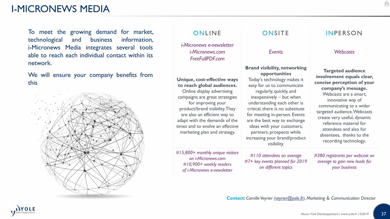
I-MICRONEWS MEDIA
To meet the growing demand for market,
technological and business information,
i-Micronews Media integrates several tools
able to reach each individual contact within its
network.
We will ensure your company benefits from
this
ONL INE ONS ITE INPERSON
i-Micronews e-newsletter
i-Micronews.com
FreeFullPDF.com
Events Webcasts
Unique, cost-effective ways
to reach global audiences.
Online display advertising
campaigns are great strategies
for improving your
product/brand visibility. They
are also an efficient way to
adapt with the demands of the
times and to evolve an effective
marketing plan and strategy.
Brand visibility, networking
opportunities
Today's technology makes it
easy for us to communicate
regularly, quickly, and
inexpensively – but when
understanding each other is
critical, there is no substitute
for meeting in-person. Events
are the best way to exchange
ideas with your customers,
partners, prospects while
increasing your brand/product
visibility.
Targeted audience
involvement equals clear,
concise perception of your
company’s message.
Webcasts are a smart,
innovative way of
communicating to a wider
targeted audience. Webcasts
create very useful, dynamic
reference material for
attendees and also for
absentees, thanks to the
recording technology.
#15,800+ monthly unique visitors
on i-Micronews.com
#10,900+ weekly readers
of i-Micronews e-newsletter
#110 attendees on average
#7+ key events planned for 2019
on different topics
#380 registrants per webcast on
average to gain new leads for
your business
Contact: Camille Veyrier ([email protected]), Marketing & Communication Director
About Yole Développement | www.yole.fr | ©2019
38
CONTACT INFORMATION
o CONSULTING AND SPECIFIC ANALYSIS, REPORT BUSINESS
• North America:
• Steve LaFerriere, Senior Sales Director for Western US & Canada
Email: [email protected] – + 1 310 600-8267
• Chris Youman, Senior Sales Director for Eastern US & Canada
Email: [email protected] – +1 919 607 9839
• Japan & Rest of Asia:
• Takashi Onozawa, General Manager, Asia Business Development
(India & ROA)
Email: [email protected] - +81 34405-9204
• Miho Othake, Account Manager (Japan)
Email: [email protected] - +81 3 4405 9204
• Itsuyo Oshiba, Account Manager (Japan & Singapore)
Email: [email protected] - +81-80-3577-3042
• Korea: Peter Ok, Business Development Director
Email: [email protected] - +82 10 4089 0233
• Greater China: Mavis Wang, Director of Greater China Business
Development
Email: [email protected] - +886 979 336 809
• Europe: Lizzie Levenez, EMEA Business Development Manager
Email: [email protected] - +49 15 123 544 182
• RoW: Jean-Christophe Eloy, CEO & President, Yole Développement
Email [email protected] - +33 4 72 83 01 80
o FINANCIAL SERVICES (in partnership with Woodside Capital
Partners)
• Jean-Christophe Eloy, CEO & President
Email: [email protected] - +33 4 72 83 01 80
• Ivan Donaldson, VP of Financial Market Development
Email: [email protected] - +1 208 850 3914
o CUSTOM PROJECT SERVICES
• Jérome Azémar, Technical Project Development Director
Email: [email protected] - +33 6 27 68 69 33
o GENERAL
• Camille Veyrier, Director, Marketing & Communication
Email: [email protected] - +33 472 83 01 01
• Sandrine Leroy, Director, Public Relations
Email: [email protected] - +33 4 72 83 01 89 / +33 6 33 11 61 55
• Email: [email protected] - +33 4 72 83 01 80
Follow us on


![Wide-Bandga 16.Wide-BandgapII-VISemiconductors ... · molecular-beam epitaxy (MBE) [16.3], metalorganic molecular-beam epitaxy (MOMBE) [16.4] and atomic-layer epitaxy (ALE) [16.5]](https://img.pdfslide.us/doc/110x75/5e1f371b74bffa7fb71fc624/wide-bandga-16wide-bandgapii-visemiconductors-molecular-beam-epitaxy-mbe.jpg)