Embed Size (px)
Citation preview
1 | P a g e
EMBEDDED SYSTEM DESIGN FOR A DIGITAL MULTIMETER USING MOTOROLA
HCS12 MICROCONTROLLER
A Thesis Submitted in partial Fulfillment
Of the Requirements of the Degree of
Bachelor of Technology
In
Electronics And Communication Engineering
Submitted by
Mr. Avinash Beck
(111EI0241)
Under the guidance of
Prof. Dr. K.K. Mahapatra
Dept. of Electronics And Communication Engineering
National Institute of Technology, Rourkela
2 | P a g e
Department of Electronics & Communication Engineering
National Institute of Technology, Rourkela
CERTIFICATE
This is to certify that this thesis entitled,” Embedded System Design for Digital Multimeter
using Motorola HCS12 microcontroller” submitted by Mr. Avinash Beck is a record of an
original research work carried out by him under my supervision and guidance in partial
fulfillment of the requirements for the award of Bachelor of Technology Degree in
Electronics & Instrumentation Engineering at the National Institute of
Technology, Rourkela.
To the best of my knowledge, the matter embodied in the thesis has not been submitted to any other
University / Institute for the award of any Degree or Diploma.
Date: Prof. Dr. K.K.Mahapatra Dept. of Electronics and Communication Engineering
National Institute of Technology Rourkela – 769008

3 | P a g e
ACKNOWLEDGEMENT
I would like to express my gratitude to my project guide Prof.Dr.
K.K Mahapatra who has always been a constant motivation and
guiding factor throughout the project time in and out as well. I am
indebted to him for giving me this opportunity. It has been a great
pleasure for me to get a chance to work under him and complete the
project. It has been an invaluable learning experience. His immense
knowledge, technical skills and human values are a source of
inspiration for all of us.
Next, I need to express my regards to my friends and my loving
parents for showing me furthermore aiding me how to learn. They
have been awesome wellsprings of motivation to me and I express my
gratitude towards them.
Date Avinash Beck
4 | P a g e
Contents LIST OF TABLES AND FIGURES ................................................................................................................. 5
ABSTRACT ................................................................................................................................................ 6
CHAPTER 1 .............................................................................................................................................. 7
HARDWARE AND SOFTWARE REQUIREMENTS ................................................................................... 8
BASIC DESIGN OF DIGITAL MULTIMETER ............................................................................................ 8
Specification of a general multimeter ................................................................................................ 9
THEORY ............................................................................................................................................. 10
CHAPTER 2 ............................................................................................................................................ 12
MICROCONTROLLER OVERVIEW ....................................................................................................... 13
PORT SYSTEM .................................................................................................................................... 14
ANALOG TO DIGITAL CONVERSION SYSTEM ..................................................................................... 15
HCS 12 Analog to Digital Conversion System .................................................................................... 17
LCD INTERFACING ............................................................................................................................. 18
4 Bit LCD Interfacing.......................................................................................................................... 22
CHAPTER 3 ............................................................................................................................................ 23
PROGRAMMING LANGUAGE ............................................................................................................ 24
CIRCUIT DESIGNS FOR SIGNAL CONDITIONING ................................................................................ 25
CONCLUSION ..................................................................................................................................... 29
REFERENCES ...................................................................................................................................... 30
5 | P a g e
LIST OF TABLES AND FIGURES
FIGURES
Fig 1. Block diagram
Fig.2 Digital Multimeter
Fig.3. SAR Converter
FIG 4. Liquid Crystal Display
Fig 5. Differential Amplifier Signal Conditioning Circuit for DC voltage Fig 6.Circuit Design for DC current measurement Fig 7. Images of circuit and results TABLES Table.1. SAR example Table.2. Pin details Table.3. List of LCD commands Table 4. Results of signal conditioning circuit of DC voltage
Table 5. Results of the Signal Conditioning Circuit for DC current
6 | P a g e
ABSTRACT The goal of this project is to develop a digital multimeter using
Motorola HCS12 microcontroller. This multimeter consists of a
number of small modules such as a signal conditioning module for
various types of input signal, an analog to digital converter (ADC) for
signal conversion and a display. The signal conditioning circuit is
made up of analog components whose parameters can be changed
to measure across a large range. The signal is then passed to an ADC
of the microcontroller. The microcontroller is programmed to
analyse the values and display the result using a display device like
LCD display.

7 | P a g e
CHAPTER 1
INTRODUCTION
8 | P a g e
HARDWARE AND SOFTWARE REQUIREMENTS
To develop this multimeter we required
Analog components to develop the signal conditioning circuit.
Motorola M68912DP256 microcontroller
Freescale Codewarrior Development Studio for HCS12(x).
LCD display
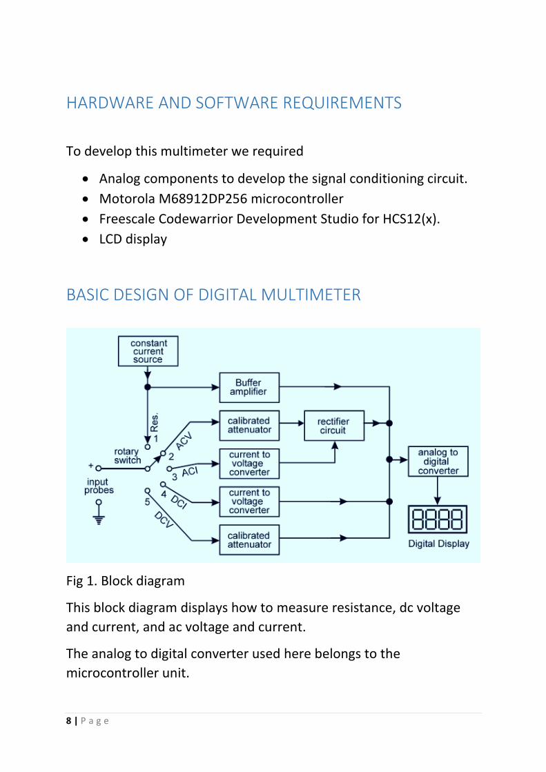
BASIC DESIGN OF DIGITAL MULTIMETER
Fig 1. Block diagram
This block diagram displays how to measure resistance, dc voltage
and current, and ac voltage and current.
The analog to digital converter used here belongs to the
microcontroller unit.
9 | P a g e
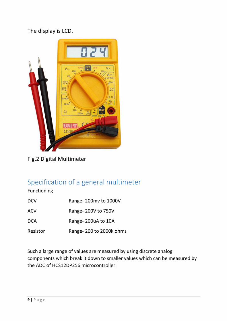
The display is LCD.
Fig.2 Digital Multimeter
Specification of a general multimeter Functioning
DCV Range- 200mv to 1000V
ACV Range- 200V to 750V
DCA Range- 200uA to 10A
Resistor Range- 200 to 2000k ohms
Such a large range of values are measured by using discrete analog
components which break it down to smaller values which can be measured by
the ADC of HCS12DP256 microcontroller.
10 | P a g e
THEORY
Measurement of resistance
An unknown resistor is connected across its input probes. The rotary
switch is in the position 1. From constant current source, a proportional
current flows through the resistor. Voltage is generated across due to the
Ohm’s Law. This voltage is directly proportional to its resistance. This voltage is
buffered and fed to A-D converter and the result is displayed in Ohms.
Measurement of DC voltage
An unknown DC voltage is connected across input probes. The rotary
switch is kept in position 5. If the voltage to be measured is larger than the
ADC reference, it is attenuated by the signal processing circuit and fed into the
ADC to get the digital reading in Volts.
Measurement of DC current
The DC current is measured indirectly. An unknown DC current is
connected across input probes. The rotary switch is kept in position-4. The
current is converted into voltage with the help of I-V converter in the signal
conditioning components. Now this voltage is fed to A-D converter to get the
digital display in Amperes.
Measurement of AC voltage
An unknown AC voltage is connected across the input probes. The rotary
switch is kept in position 2. If the voltage is above the selected range and then
it is attenuated and then rectified to convert it into proportional DC voltage. It
is then fed to ADC to get the digital reading in Volts.
Measurement of AC current
Current is measured by converting it into proportional voltage. An
unknown AC current is connected across input probes. The rotary switch is
kept in position 3. The current is converted into proportional voltage with the
help of I-V converter and then rectified by the signal conditioning circuitry.
Now the voltage in terms of AC current is fed to ADC to get digital reading in
Amperes.
11 | P a g e
So, in the above, we learnt how to measure five very important parameters of
every circuit. This are the most basic functions of multimeters. Modern digital
multimeters provide a vast range of measuring capabilities like
1. Capacitance 2. Temperature 3. Frequency 4. Transistor test 5. Continuity (buzzer)
There are many high end digital multimeter that provide better functions like auto-ranging. This DMM can sense from the input and choose the correct range for the value. Manual selection of the particular type of measurement to be made is still required.
Auto-polarity is another feature. This enables the Digital Multimeter to indicate the polarity of the reading with respect to its input connections without the need change the terminals.
12 | P a g e
CHAPTER 2
FREESCALE HCS12 MICROCONTROLLER SYSTEM
13 | P a g e
MICROCONTROLLER OVERVIEW The MC9S12DP256 microcontroller unit (MCU) is a 16-bit microcontroller having multiple onboard peripherals with a 16-bit central processing unit (HCS12 CPU). Its features are; 256K bytes of Flash EEPROM 12K bytes of RAM 4K bytes of EEPROM two asynchronous serial communications interfaces (SCI) three serial peripheral interfaces (SPI) an 8-channel IC/OC enhanced capture timer two 8-channel, 10-bit analog-to-digital converters (ADC) an 8-channel pulse-width modulator (PWM) a digital Byte Data Link Controller (BDLC) 29 discrete digital I/O channels
20 discrete digital I/O lines with interrupt and wakeup capability
five CAN 2.0 A, B software compatible modules (MSCAN12) and an Inter-IC Bus.
The MC9S12DP256 has full 16-bit data paths. The external bus can also operate in an 8-bit narrow mode for lower cost or older systems with 8 bit memory. It is manufactured by Freescale Semiconductors and are used in a wide range of application.
14 | P a g e
PORT SYSTEM • Port A: General purpose I/O. Equipped with DDR to set I/O
configuration to each pin.
• Port B: General purpose I/O. Equipped with DDR to set I/O
configuration to each pin.
• Port E: Used for mode selection, bus control signal, initiate
external interrupt.
• Port AD: Input for ADC system.
• Port T: Used as input capture and output compare pins for
Timer System.
• Port S: Used for Serial Communication Interface & Serial
Peripheral Interface.
• Port P: Used to interface with Pulse Width Modulation System.
• Port DLC: Interface to Byte Data Link Communication (BDLC)
System.
In this project, we have to design a multimeter. So we need to be
acquainted to the uses to different ports. The AD Port, is primarily
used for ADC application. There are some other ports which will be
used for LCD interfacing.
15 | P a g e
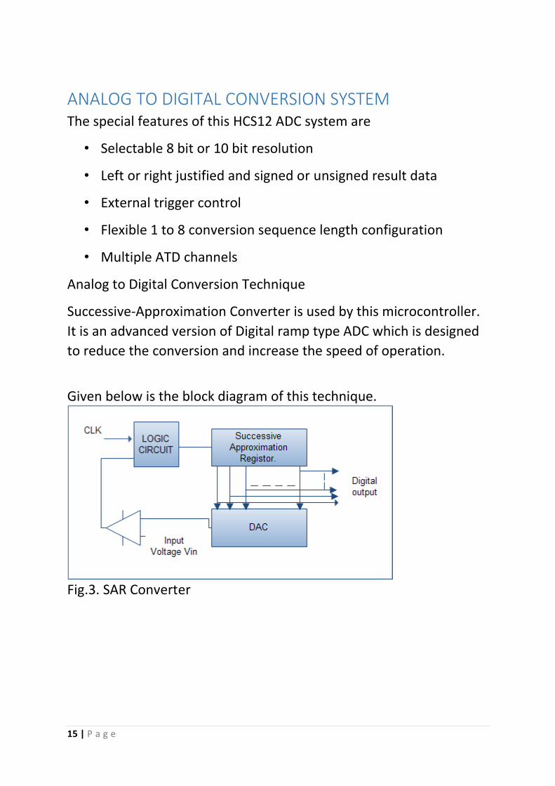
ANALOG TO DIGITAL CONVERSION SYSTEM The special features of this HCS12 ADC system are
• Selectable 8 bit or 10 bit resolution
• Left or right justified and signed or unsigned result data
• External trigger control
• Flexible 1 to 8 conversion sequence length configuration
• Multiple ATD channels
Analog to Digital Conversion Technique
Successive-Approximation Converter is used by this microcontroller.
It is an advanced version of Digital ramp type ADC which is designed
to reduce the conversion and increase the speed of operation.
Given below is the block diagram of this technique.
Fig.3. SAR Converter
16 | P a g e
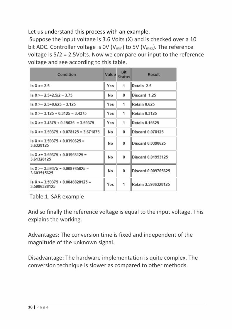
Let us understand this process with an example. Suppose the input voltage is 3.6 Volts (X) and is checked over a 10 bit ADC. Controller voltage is 0V (Vmin) to 5V (Vmax). The reference voltage is 5/2 = 2.5Volts. Now we compare our input to the reference voltage and see according to this table.
Table.1. SAR example And so finally the reference voltage is equal to the input voltage. This explains the working. Advantages: The conversion time is fixed and independent of the magnitude of the unknown signal. Disadvantage: The hardware implementation is quite complex. The conversion technique is slower as compared to other methods.
17 | P a g e
HCS 12 Analog to Digital Conversion System The steps to convert to ATD voltage are-
1. The ADPU bit in ATDCTL2 must be set to 1 to turn on the ADC. 2. Wait for 100us after setting ADPU to allow the ADC to settle. 3. Decide the type of ATD conversion by using the control
registers. 4. Set the ATDCTL5 register and check if the SCF bit of ATDSTAT
register is active. 5. Check the ATD result register.
The registers used in the HCS12 ADC system are
1. Control register- Registers that are used to tailor an ATD conversion sequence to user specification.
2. Status register- Register containing a series of flags that indicate the status of ATD system.
3. Result register- Eight identical 8 bit register that store the value generated by the ADC.
4. Test register- 2-byte ATD test register that can only be read from or written to in special modes.
Now, we are going to write the code for ADC of the signal generated from the signal conditioning circuit. This digital output is now represented by any display device like LCD.
18 | P a g e
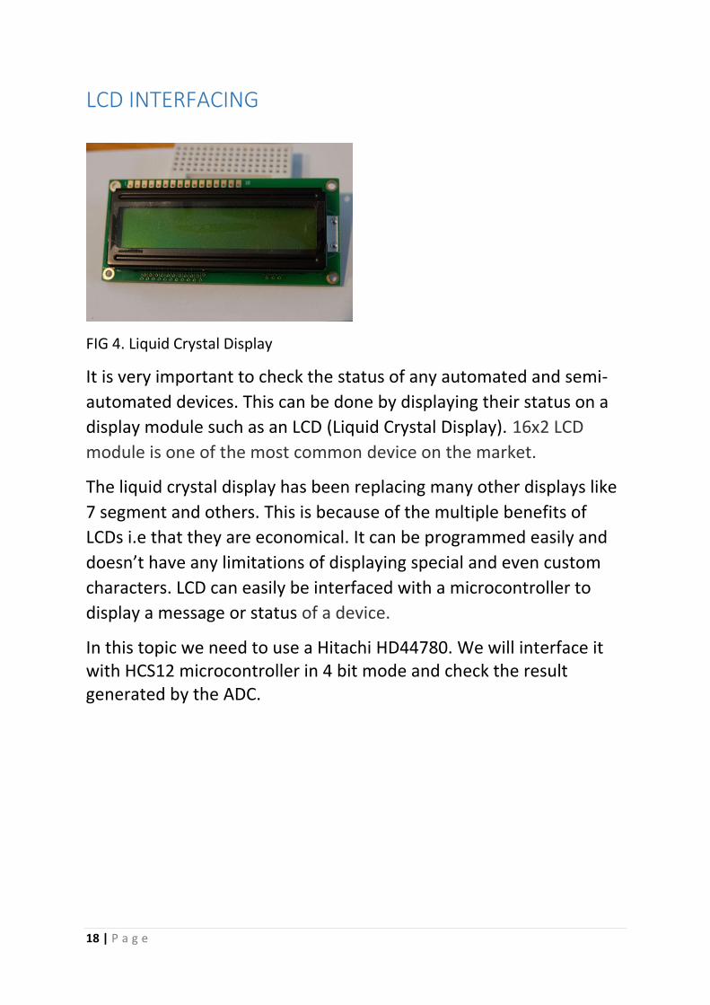
LCD INTERFACING
FIG 4. Liquid Crystal Display
It is very important to check the status of any automated and semi-
automated devices. This can be done by displaying their status on a
display module such as an LCD (Liquid Crystal Display). 16x2 LCD
module is one of the most common device on the market.
The liquid crystal display has been replacing many other displays like
7 segment and others. This is because of the multiple benefits of
LCDs i.e that they are economical. It can be programmed easily and
doesn’t have any limitations of displaying special and even custom
characters. LCD can easily be interfaced with a microcontroller to
display a message or status of a device.
In this topic we need to use a Hitachi HD44780. We will interface it with HCS12 microcontroller in 4 bit mode and check the result generated by the ADC.
19 | P a g e
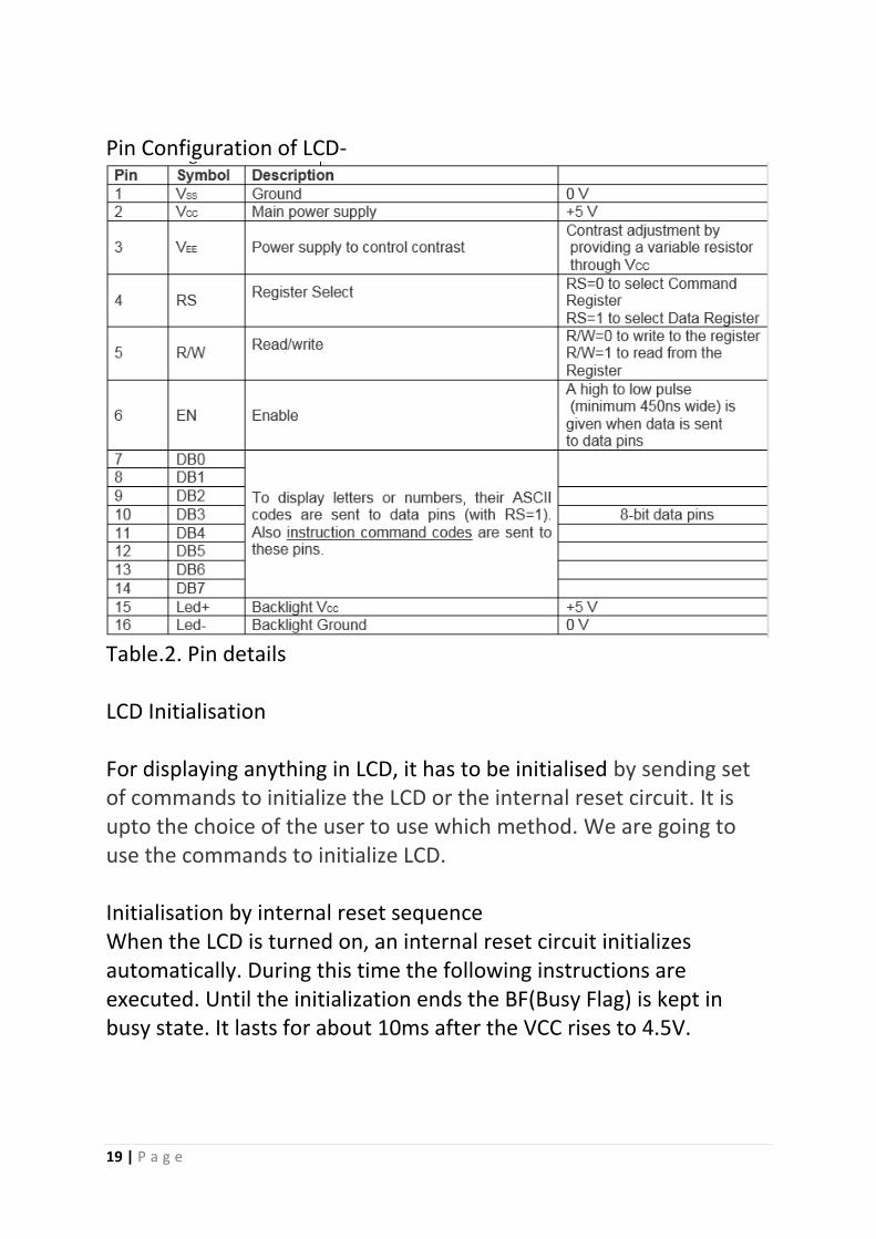
Pin Configuration of LCD-
Table.2. Pin details LCD Initialisation For displaying anything in LCD, it has to be initialised by sending set of commands to initialize the LCD or the internal reset circuit. It is upto the choice of the user to use which method. We are going to use the commands to initialize LCD. Initialisation by internal reset sequence When the LCD is turned on, an internal reset circuit initializes automatically. During this time the following instructions are executed. Until the initialization ends the BF(Busy Flag) is kept in busy state. It lasts for about 10ms after the VCC rises to 4.5V.
20 | P a g e
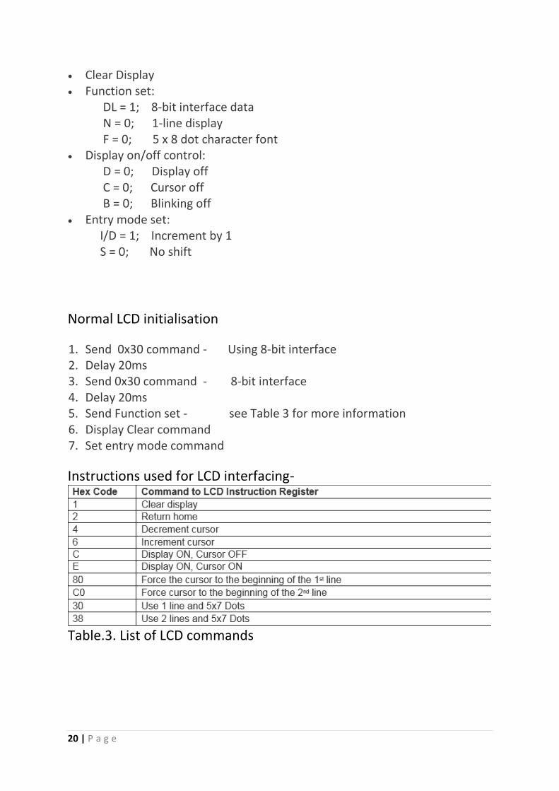
Clear Display Function set:
DL = 1; 8-bit interface data N = 0; 1-line display F = 0; 5 x 8 dot character font
Display on/off control: D = 0; Display off C = 0; Cursor off B = 0; Blinking off
Entry mode set: I/D = 1; Increment by 1 S = 0; No shift
Normal LCD initialisation
1. Send 0x30 command - Using 8-bit interface 2. Delay 20ms 3. Send 0x30 command - 8-bit interface 4. Delay 20ms 5. Send Function set - see Table 3 for more information 6. Display Clear command 7. Set entry mode command
Instructions used for LCD interfacing-
Table.3. List of LCD commands
21 | P a g e
To successfully process the command or data, a delay is needed. Such a delay can be created by a delay loop of the required time which is greater than the time required to process the command or by reading the busy flag. The latter method is usually recommended. The reason to use busy flag is that delay produced is the exact amount of time for which LCD need to process the time. So is best suited for every application. These are steps to read a busy flag
1. Select command register 2. Select read operation 3. Send enable signal 4. Read the flag
Move data to LCD port
1. select command register 2. select write operation 3. send enable signal 4. wait for LCD to process the command
Sending Data to LCD
To send data we simply need to select the data register. Following are the steps:
1. Move data to LCD port 2. select data register 3. select write operation 4. send enable signal 5. wait for LCD to process the data
22 | P a g e
4 Bit LCD Interfacing
There are many reasons why sometime we prefer to use LCD in 4-bit mode instead of 8-bit. One basic reason is lesser number of pins are needed to interface.
Only 6 pins are needed in this process to interface an LCD. The unwanted data pins of LCD i.e. D0-D3 are connected to ground. D4-D7 are the pins used for data transfer in nibble. Enable and register select are the LCD control pins and are also connected to the controller. The Read/Write (RW) Pin of the LCD are not used, as we are only writing on the LCD. So this pin is grounded. In case you want to read from LCD, this pin is also connected. In this process an extra pin is also required which is not needed in this project. Potentiometer RV1 is used to control the LCD contrast.
After the connections are made, now the data has to be send. In this mode the
data is sent in nibbles. In the beginning a higher nibble is send followed by a
lower nibble. A special sequence of initialization is followed to used to enable 4
bit mode. Now the LCD controller knows that user has selected 4-bit mode of
operation. This special sequence is called as resetting the LCD.
Following is the reset sequence of LCD.
1. Wait 20mS
2. Send instruction value (0x30)
3. Wait 10mS
4. Send instruction value (0x30)
5. Wait 1mS
6. Send instruction value (0x30)
7. Wait 1mS
8. Select bus width (0x30 - for 8-bit and 0x20 for 4-bit)
9. Wait 1mS
23 | P a g e
CHAPTER 3
IMPLEMENTATION

24 | P a g e
PROGRAMMING LANGUAGE
CodeWarrior Development Studios
This is the software used to program the freescale HCS12 microcontroller.
Freescale’s Codewarrior Development Studios provide the tools to enable the
design with Freescale microcontrollers. It contains a standalone C cross-
compiler, pre-processor, assembler, linker, simulator, and debugger for use
with freescale microcontroller boards. Such tools are highly essential for
engineers in the development of products. Any team can reuse the features of
a common project and work on the project already completed by the previous
team.
25 | P a g e
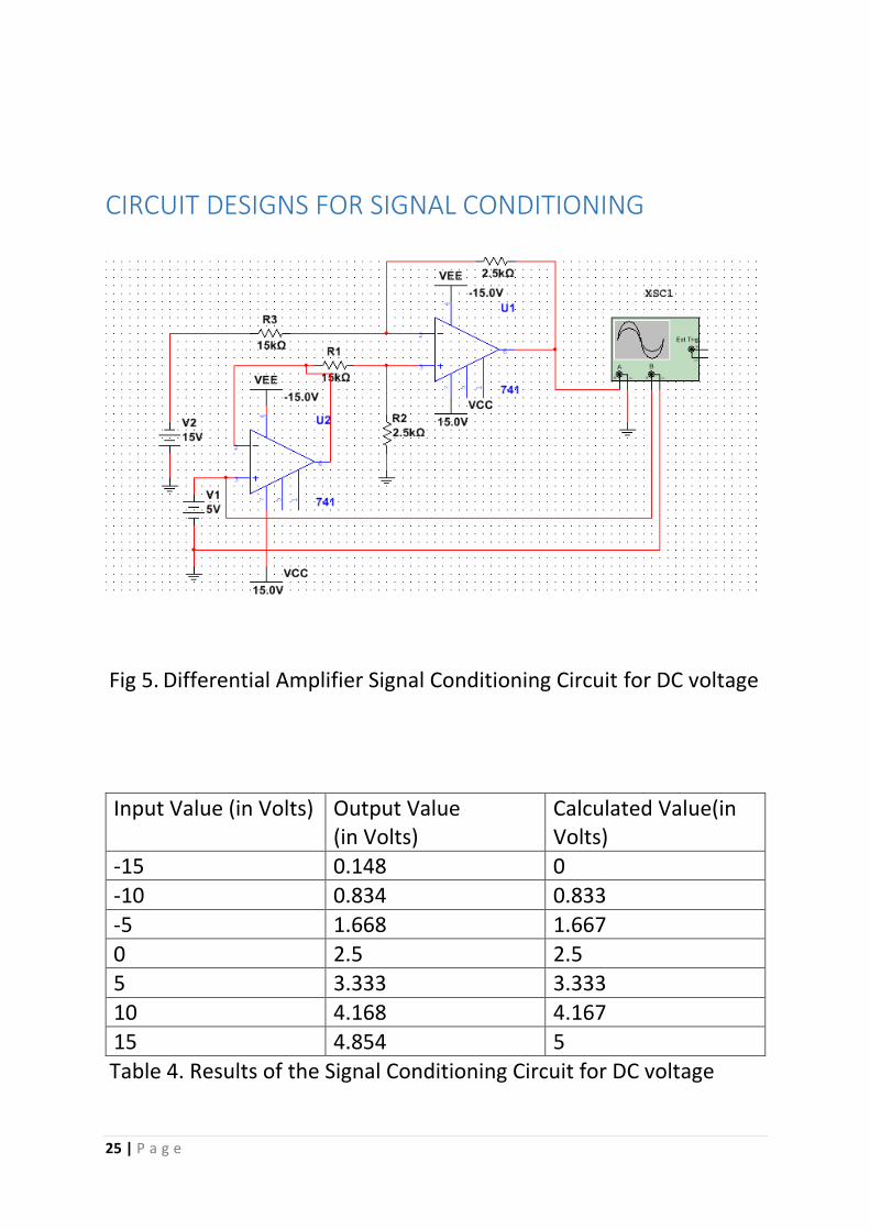
CIRCUIT DESIGNS FOR SIGNAL CONDITIONING
Fig 5. Differential Amplifier Signal Conditioning Circuit for DC voltage
Input Value (in Volts) Output Value (in Volts)
Calculated Value(in Volts)
-15 0.148 0
-10 0.834 0.833
-5 1.668 1.667
0 2.5 2.5 5 3.333 3.333
10 4.168 4.167
15 4.854 5
Table 4. Results of the Signal Conditioning Circuit for DC voltage
26 | P a g e
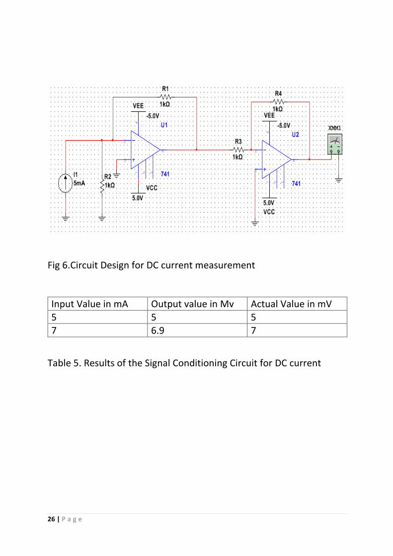
Fig 6.Circuit Design for DC current measurement
Input Value in mA Output value in Mv Actual Value in mV
5 5 5
7 6.9 7
Table 5. Results of the Signal Conditioning Circuit for DC current
27 | P a g e
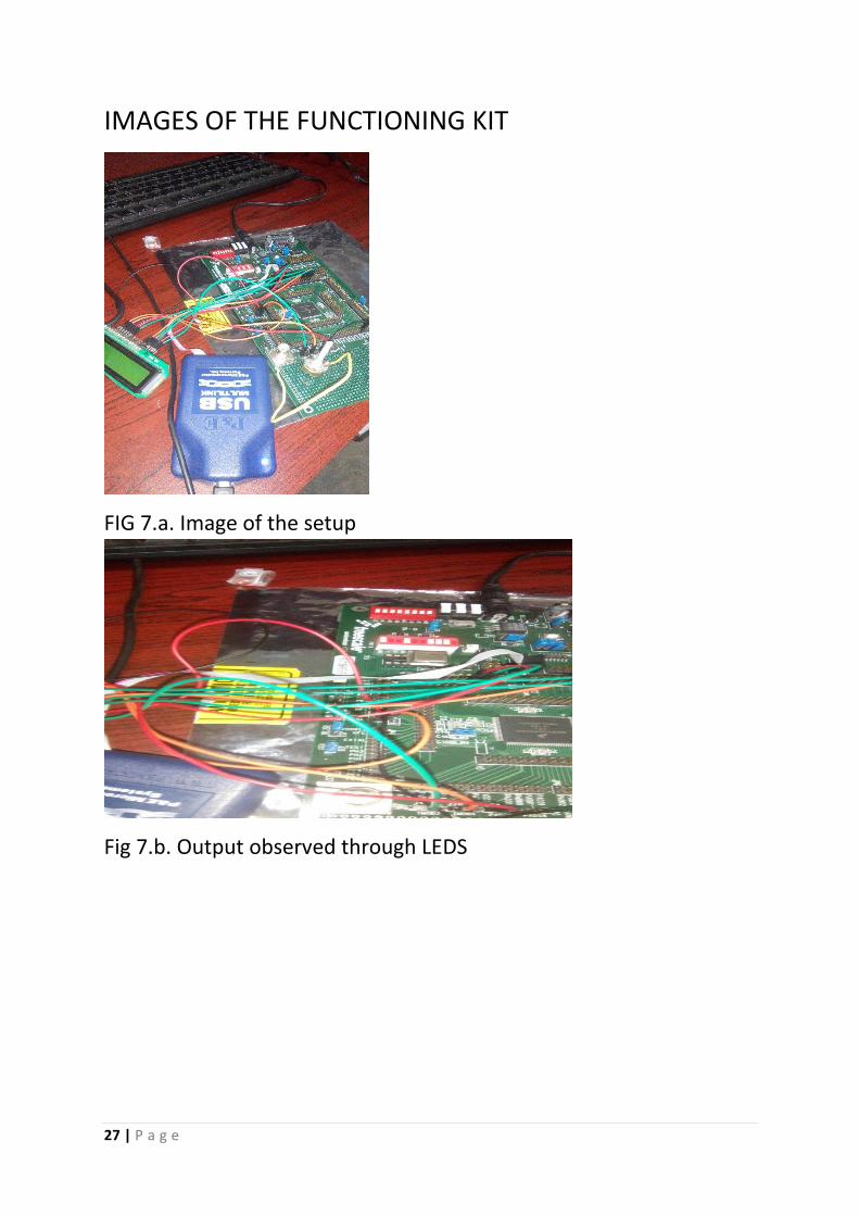
IMAGES OF THE FUNCTIONING KIT
FIG 7.a. Image of the setup
Fig 7.b. Output observed through LEDS
28 | P a g e
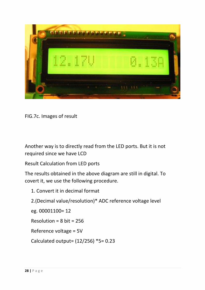
FIG.7c. Images of result
Another way is to directly read from the LED ports. But it is not
required since we have LCD
Result Calculation from LED ports
The results obtained in the above diagram are still in digital. To
covert it, we use the following procedure.
1. Convert it in decimal format
2.(Decimal value/resolution)* ADC reference voltage level
eg. 00001100= 12
Resolution = 8 bit = 256
Reference voltage = 5V
Calculated output= (12/256) *5= 0.23
29 | P a g e
CONCLUSION
A simple multimeter was successfully designed. The proposed digital
multimeter can work in a large range as required by changing the
signal conditioning circuit. It has a very high resolution because of 10
bit ADC. However, since it is designed on a HCS12DP256
microcontroller board, the cost is very high. The aim of this project
was to learn about this new microcontroller which is new in the
market and whose proper documentation is not available. With
proper reduction of board size and PCB design there can be a
significant reduction of price.
30 | P a g e
REFERENCES
1. Barrett, Steven F. and Pack, Daniel J., Embedded Systems Design
and Applications with the 68HC12 and HCS12
2. Datasheet for M68912DP256
3.http://www.eee.metu.edu.tr/~ee214/documents/NotesOnMult
imete rs.pdf
4. http://www.freescale.com
5. http://www.engineersgarage.com