Embed Size (px)
Citation preview
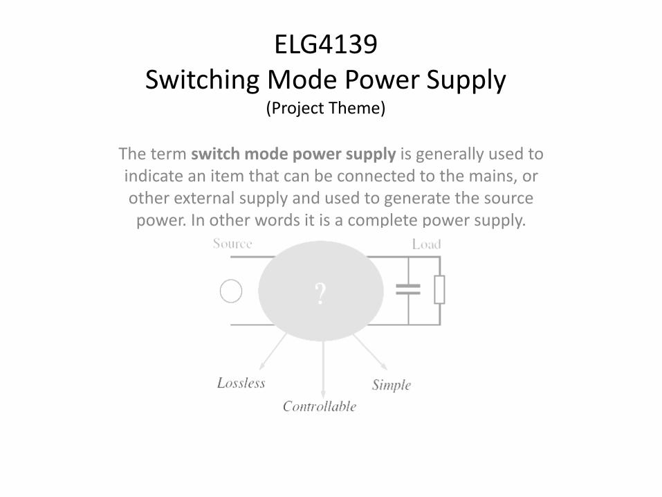
ELG4139 Switching Mode Power Supply
(Project Theme)
The term switch mode power supply is generally used to indicate an item that can be connected to the mains, or other external supply and used to generate the source power. In other words it is a complete power supply.
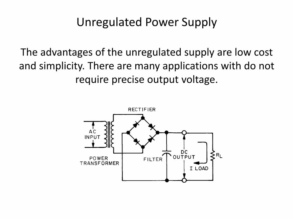
Unregulated Power Supply
The advantages of the unregulated supply are low cost and simplicity. There are many applications with do not
require precise output voltage.
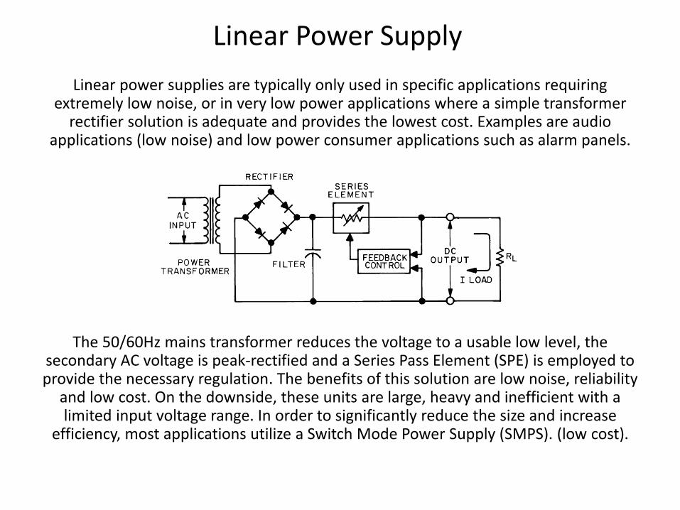
Linear Power Supply
Linear power supplies are typically only used in specific applications requiring extremely low noise, or in very low power applications where a simple transformer
rectifier solution is adequate and provides the lowest cost. Examples are audio applications (low noise) and low power consumer applications such as alarm panels.
The 50/60Hz mains transformer reduces the voltage to a usable low level, the secondary AC voltage is peak-rectified and a Series Pass Element (SPE) is employed to provide the necessary regulation. The benefits of this solution are low noise, reliability
and low cost. On the downside, these units are large, heavy and inefficient with a limited input voltage range. In order to significantly reduce the size and increase
efficiency, most applications utilize a Switch Mode Power Supply (SMPS). (low cost).
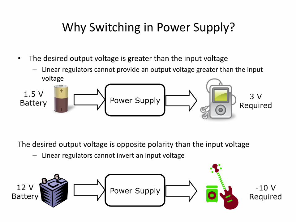
Why Switching in Power Supply?
• The desired output voltage is greater than the input voltage
– Linear regulators cannot provide an output voltage greater than the input voltage
The desired output voltage is opposite polarity than the input voltage
– Linear regulators cannot invert an input voltage
1.5 V Battery Power Supply
3 V Required
Power Supply 12 V Battery
-10 V Required
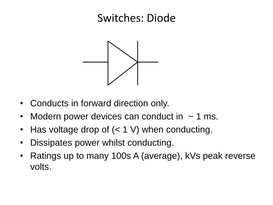
Switches: Diode
• Conducts in forward direction only.
• Modern power devices can conduct in ~ 1 ms.
• Has voltage drop of (< 1 V) when conducting.
• Dissipates power whilst conducting.
• Ratings up to many 100s A (average), kVs peak reverse
volts.
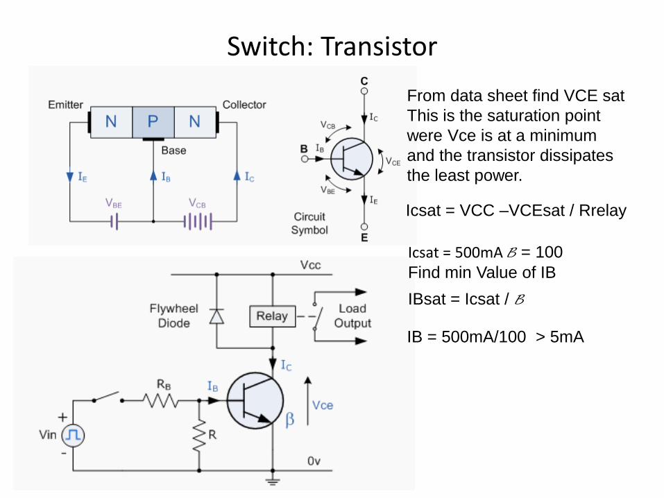
Switch: Transistor
From data sheet find VCE sat
This is the saturation point
were Vce is at a minimum
and the transistor dissipates
the least power.
Icsat = VCC –VCEsat / Rrelay
Icsat = 500mA B = 100
Find min Value of IB
IBsat = Icsat / B
IB = 500mA/100 > 5mA
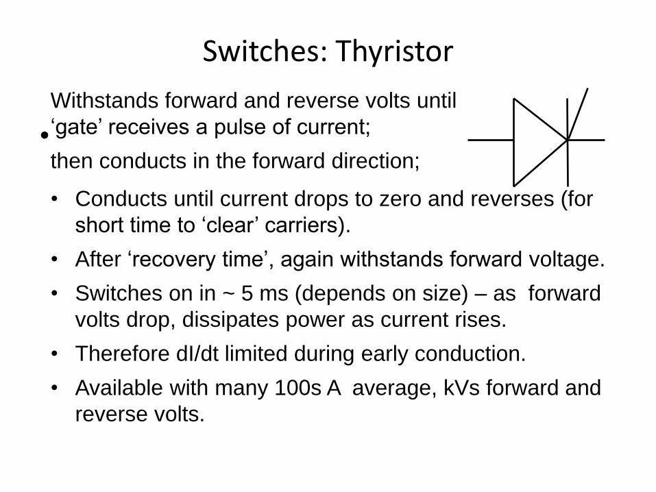
Switches: Thyristor
•
Withstands forward and reverse volts until
‘gate’ receives a pulse of current;
then conducts in the forward direction;
• Conducts until current drops to zero and reverses (for
short time to ‘clear’ carriers).
• After ‘recovery time’, again withstands forward voltage.
• Switches on in ~ 5 ms (depends on size) – as forward
volts drop, dissipates power as current rises.
• Therefore dI/dt limited during early conduction.
• Available with many 100s A average, kVs forward and
reverse volts.
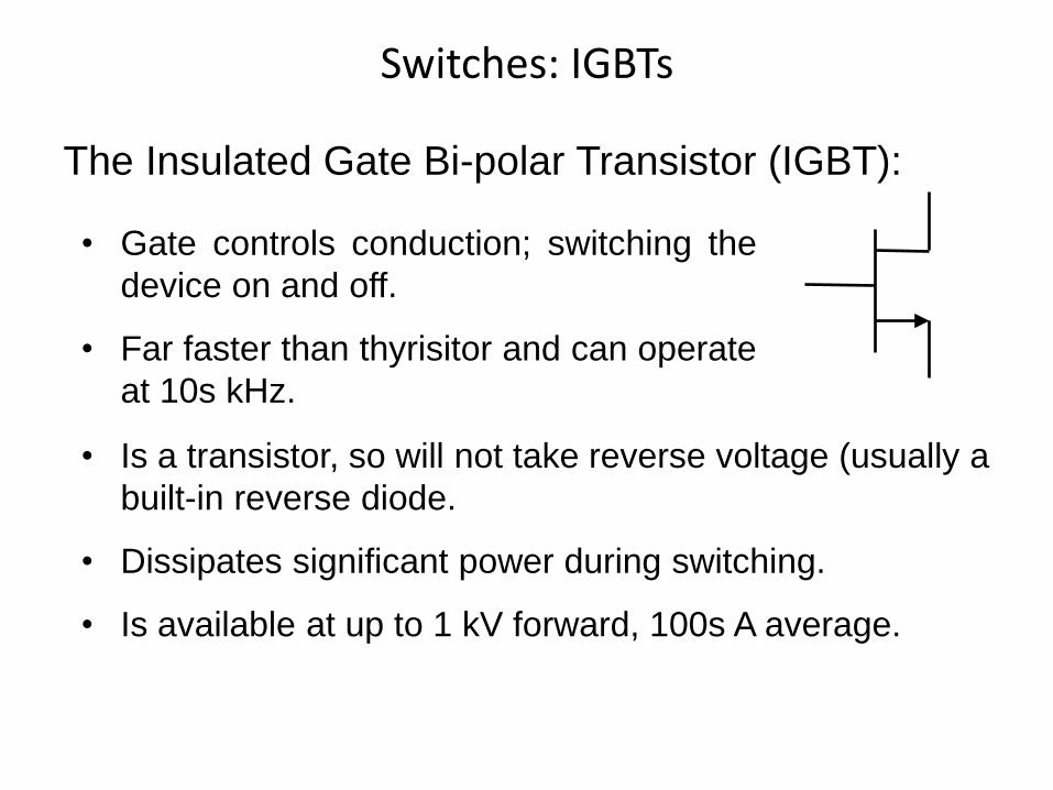
Switches: IGBTs
The Insulated Gate Bi-polar Transistor (IGBT):
• Gate controls conduction; switching the
device on and off.
• Far faster than thyrisitor and can operate
at 10s kHz.
• Is a transistor, so will not take reverse voltage (usually a
built-in reverse diode.
• Dissipates significant power during switching.
• Is available at up to 1 kV forward, 100s A average.
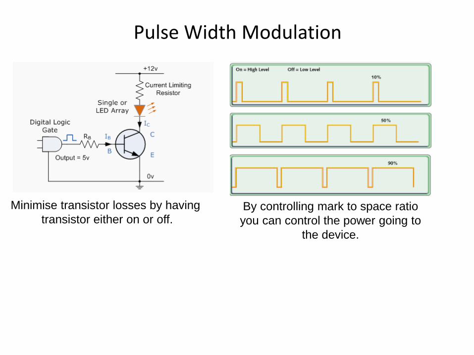
Pulse Width Modulation
By controlling mark to space ratio
you can control the power going to
the device.
Minimise transistor losses by having
transistor either on or off.
Switch Mode Power Supplies
The use of switch mode topologies has reduced the size and improved the efficiency of power supplies by increasing the
frequency of operation, reducing the physical size of transformers, inductors and capacitors, and utilizing an ‘on or
off’ switching element to increase efficiency. The compromises in adopting this technique are increased ripple and noise on the
output DC supply and the generation of both conducted and radiated EMI which have to be managed.
The introduction of low voltage semiconductors and the consequent high output current demands have driven the
development of synchronous output rectifier schemes, where the output diodes are replaced by power MOSFETs to reduce
power dissipation in the secondary and achieve high efficiency solutions for these applications.
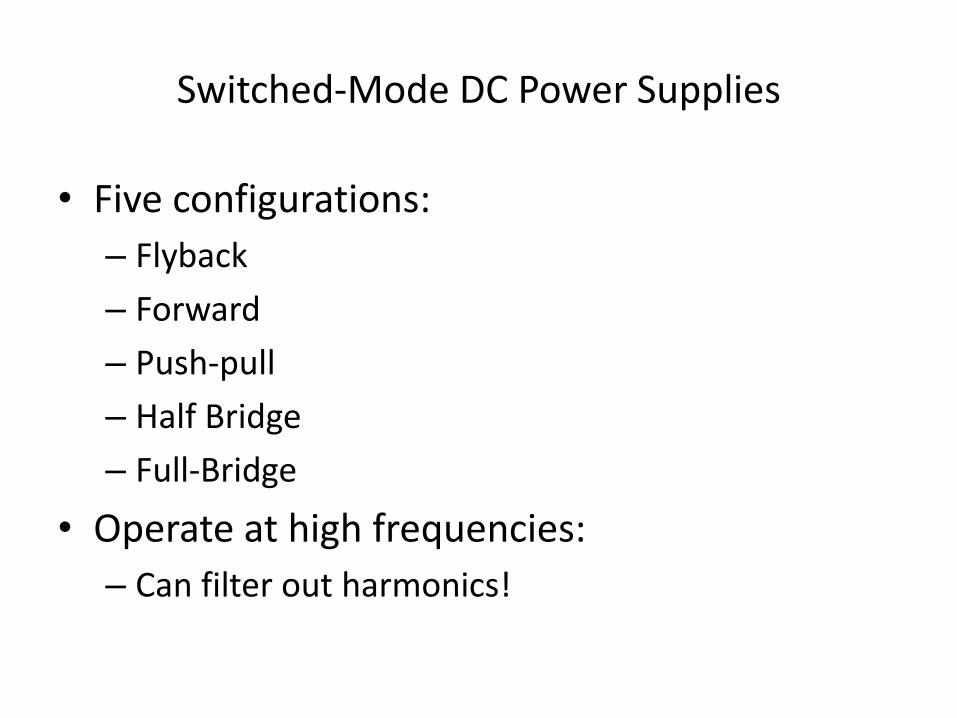
Switched-Mode DC Power Supplies
• Five configurations:
– Flyback
– Forward
– Push-pull
– Half Bridge
– Full-Bridge
• Operate at high frequencies:
– Can filter out harmonics!
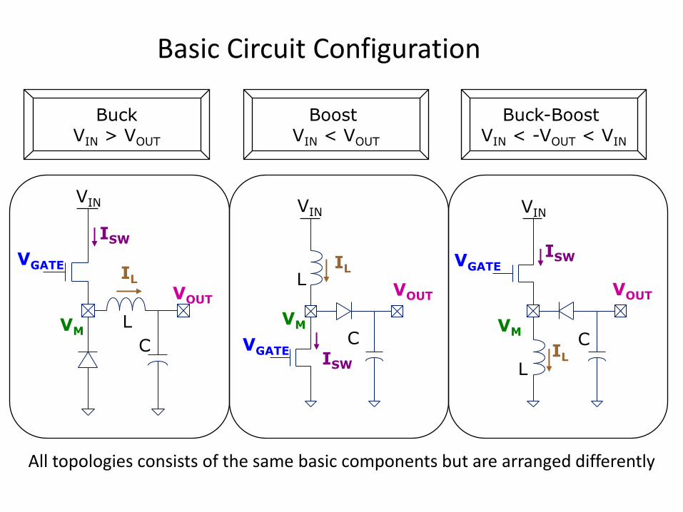
Basic Circuit Configuration
VOUT
VIN
VM
VGATE
L
C
ISW
IL VOUT
VIN
VM
C VGATE
L IL
ISW
VOUT
VIN
VM C
VGATE
L IL
ISW
Buck-Boost VIN < -VOUT < VIN
Boost VIN < VOUT
Buck VIN > VOUT
All topologies consists of the same basic components but are arranged differently
Inductor Technology
• There are a number of inductor technologies to choose from:
• Drum core
• Flat coil
• Toroid
• Bead
• Wire-wound
• Planar
• In addition to inductance and saturation current, the inductor technology will also affect:
• Inductor resistance and impedance
• Size (length, width, height)
• Cost
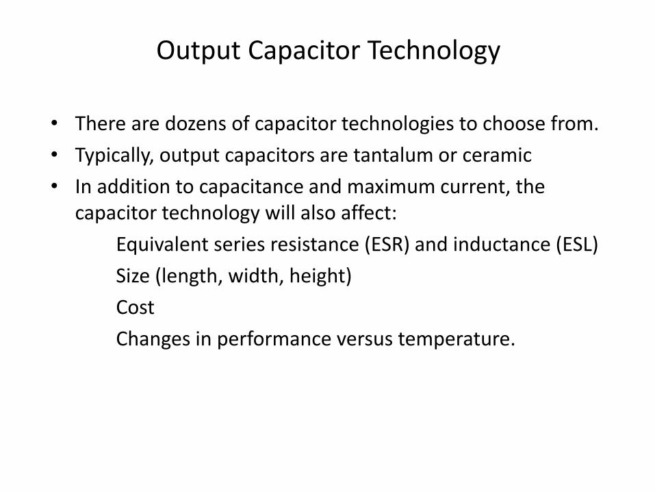
Output Capacitor Technology
• There are dozens of capacitor technologies to choose from.
• Typically, output capacitors are tantalum or ceramic
• In addition to capacitance and maximum current, the capacitor technology will also affect:
Equivalent series resistance (ESR) and inductance (ESL)
Size (length, width, height)
Cost
Changes in performance versus temperature.
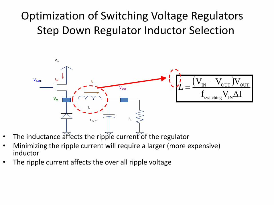
Optimization of Switching Voltage Regulators Step Down Regulator Inductor Selection
ΔIVf
VVV
INswitching
OUTOUTIN
L
• The inductance affects the ripple current of the regulator • Minimizing the ripple current will require a larger (more expensive)
inductor • The ripple current affects the over all ripple voltage
VOUT
VIN
VM
VGATE
L
COUT RL
IIN IL
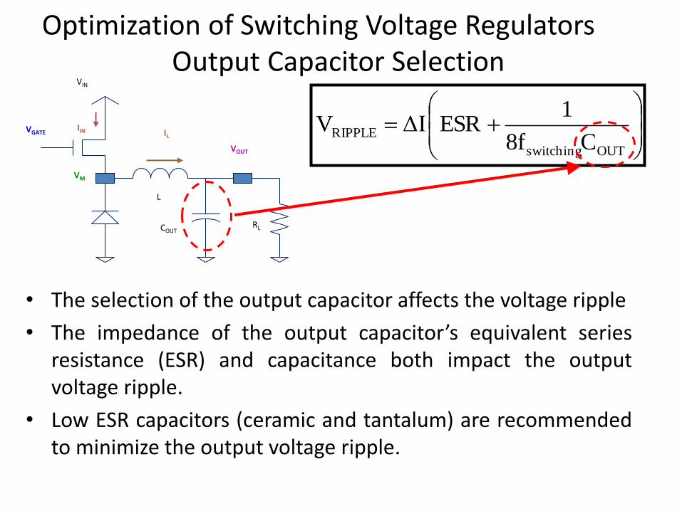
Optimization of Switching Voltage Regulators Output Capacitor Selection
OUTswitching
RIPPLEC8f
1ESRΔIV
• The selection of the output capacitor affects the voltage ripple
• The impedance of the output capacitor’s equivalent series resistance (ESR) and capacitance both impact the output voltage ripple.
• Low ESR capacitors (ceramic and tantalum) are recommended to minimize the output voltage ripple.
VOUT
VIN
VM
VGATE
L
COUT RL
IIN IL
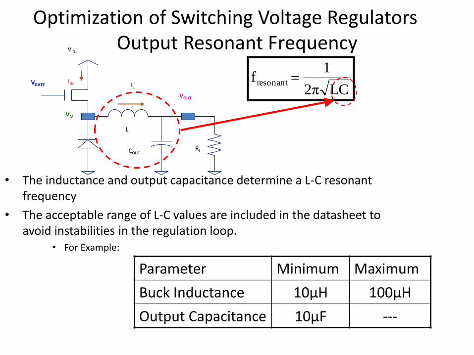
Optimization of Switching Voltage Regulators Output Resonant Frequency
LC2π
1f resonant
• The inductance and output capacitance determine a L-C resonant frequency
• The acceptable range of L-C values are included in the datasheet to avoid instabilities in the regulation loop.
• For Example:
Parameter Minimum Maximum
Buck Inductance 10µH 100µH
Output Capacitance 10µF ---
VOUT
VIN
VM
VGATE
L
COUT RL
IIN IL
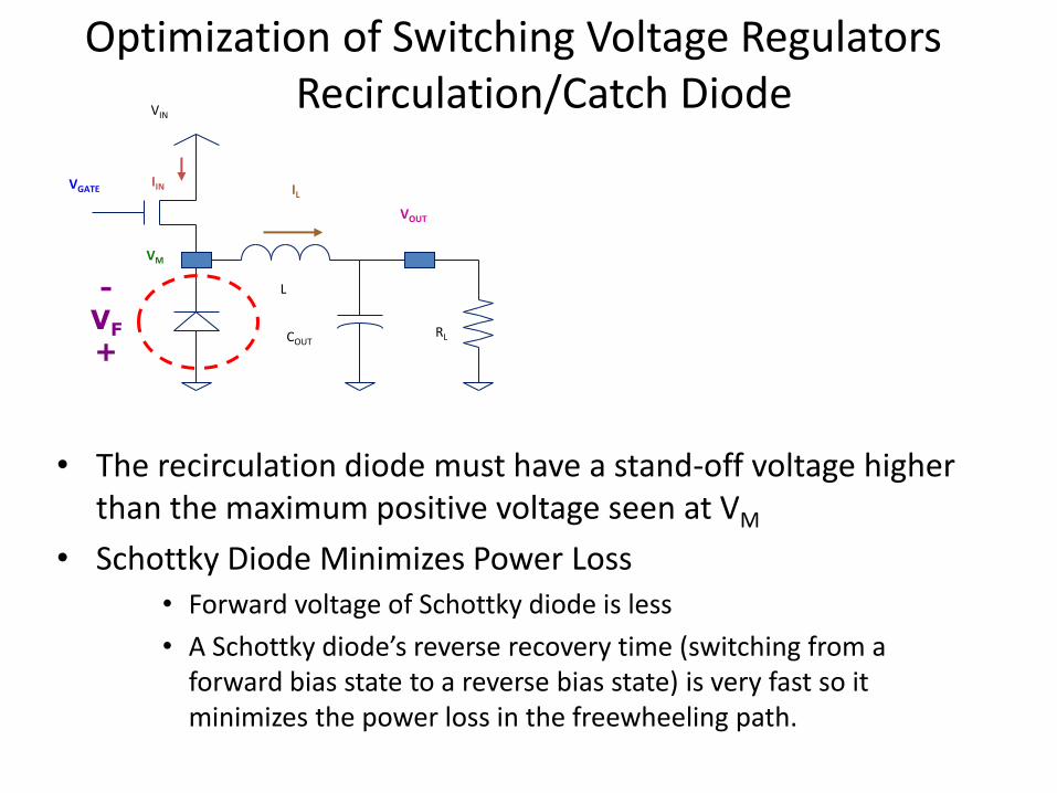
Optimization of Switching Voltage Regulators Recirculation/Catch Diode
• The recirculation diode must have a stand-off voltage higher than the maximum positive voltage seen at VM
• Schottky Diode Minimizes Power Loss • Forward voltage of Schottky diode is less
• A Schottky diode’s reverse recovery time (switching from a forward bias state to a reverse bias state) is very fast so it minimizes the power loss in the freewheeling path.
VOUT
VIN
VM
VGATE
L
COUT RL
IIN IL
- VF
+
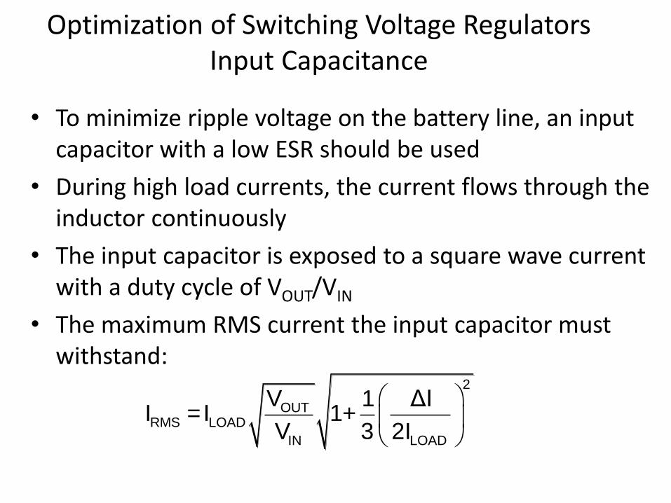
Optimization of Switching Voltage Regulators Input Capacitance
2
OUTRMS LOAD
IN LOAD
V 1 ΔII = I 1+
V 3 2I
• To minimize ripple voltage on the battery line, an input capacitor with a low ESR should be used
• During high load currents, the current flows through the inductor continuously
• The input capacitor is exposed to a square wave current with a duty cycle of VOUT/VIN
• The maximum RMS current the input capacitor must withstand:
Summary
• Switching voltage regulators convert a non-useful input voltage to a useful output voltage.
• When in regulation, the power transistor is either completely on or completely off.
• The duty cycle of the power transistor is varied to regulated the output voltage.
• Step down switching voltage regulators are used for high efficiency conversion.
• Step up switching voltage regulators are used because linear regulators cannot perform a step up conversion.
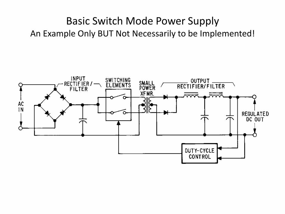
Basic Switch Mode Power Supply An Example Only BUT Not Necessarily to be Implemented!


![Circuit Switching - Signaling [Compatibility Mode]](https://img.pdfslide.us/doc/110x75/546b7050b4af9f892c8b4c91/circuit-switching-signaling-compatibility-mode.jpg)


![Chap 5 Telecom Switching [Compatibility Mode] - Copy.pdf](https://img.pdfslide.us/doc/110x75/577cd7061a28ab9e789dda1b/chap-5-telecom-switching-compatibility-mode-copypdf.jpg)