Embed Size (px)
Citation preview
A 6.39GHz-14GHz Series Resonator Mode-Switching Oscillatorwith 186-188dB FoM and 197dB FoMA in 65nm CMOS
Abhishek Agrawal, Arun NatarajanSchool of EECS, Oregon State University, Corvallis, OR, USA
Abstract — CMOS LC voltage-controlled oscillators (VCO)with octave frequency tuning-range (FTR) are attractivefor wideband radios. An area and power-efficient resonantmode-switching approach is presented that enables wide-FTRoscillators without compromising inductor Q, resulting inlow phase noise and high VCO Figure-of-Merit (FoM). Theproposed series resonator mode-switching approach results ina 6.4GHz to 14GHz VCO (74.6% FTR) in 65nm CMOS thatachieves 186dB-188dB FoM. The scalability of this approachtowards achieving even larger FTR is also demonstrated bya triple-mode 2.2GHz to 8.7GHz (119% FTR) VCO.
I. INTRODUCTION
A VCO with octave frequency tuning range (FTR)can be used in conjunction with dividers to generateall frequencies below its highest oscillation frequency.Additionally, quadrature-LO generation in integratedtransceivers is simplified with a VCO operating at 2fLO
followed by a divide-by-2. Therefore, CMOS VCOs with6GHz to 12GHz FTR are attractive for multi-standardwireless radios targeting prevalent wireless standardsbetween 400MHz to 6GHz [1]. The targeted FTR canbe achieved by multiplexing two or more LC oscillatorshowever, a single octave-FTR LC VCO that achievessimilar performance can potentially result in smaller area.
Simultaneously achieving low phase noise and wideFTR in an LC VCO with switched-capacitor tuningrequires unrealistically small inductor sizes, leading to lowtank impedance [2]. In addition, the inductor quality-factor(Q) is frequency dependent which can further decrease thelower impedance at low oscillation frequencies. Alternatetopologies with switches in series with inductors or acrosstransformers have been proposed for wide FTR, but thephase noise is limited by switch losses, particularly at highfrequencies.
A transformer-based resonator mode-switching VCOthat enables lossless mode-switching is proposedin [2], achieving excellent phase noise and VCOfigure-of-merit(FoM) across an octave FTR up to5.62GHz. This approach ensures low area overhead byplacing one transformer coil inside another - howeverthe mutual coupling that underlies the approach degradesinductor Q. An extension to three resonant modes isproposed in [3] in order to achieve octave FTR at higheroscillation frequency (∼13GHz). However, this leads to atradeoff between increased VCO area and higher power
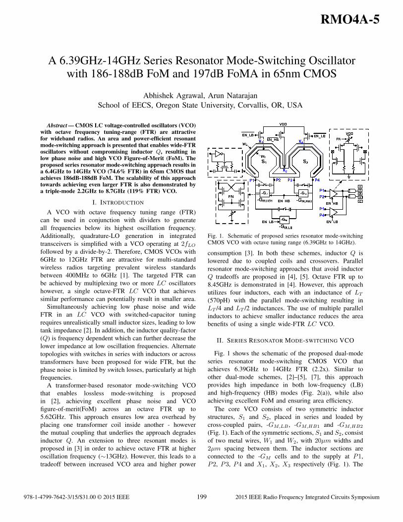
Fig. 1. Schematic of proposed series resonator mode-switchingCMOS VCO with octave tuning range (6.39GHz to 14GHz).
consumption [3]. In both these schemes, inductor Q islowered due to coupled coils and crossovers. Parallelresonator mode-switching approaches that avoid inductorQ tradeoffs are proposed in [4], [5]. Octave FTR up to8.45GHz is demonstrated in [4]. However, this approachutilizes four inductors, each with an inductance of LT
(570pH) with the parallel mode-switching resulting inLT /4 and LT /2 inductances. The use of multiple parallelinductors to achieve smaller inductance reduces the areabenefits of using a single wide-FTR LC VCO.
II. SERIES RESONATOR MODE-SWITCHING VCO
Fig. 1 shows the schematic of the proposed dual-modeseries resonator mode-switching CMOS VCO thatachieves 6.39GHz to 14GHz FTR (2.2x). Similar toother dual-mode schemes, [2]–[5], [7], this approachprovides high impedance in both low-frequency (LB)and high-frequency (HB) modes (Fig. 2(a)), while alsoachieving excellent FoM and ensuring area efficiency.
The core VCO consists of two symmetric inductorstructures, S1 and S2, placed in series and loaded bycross-coupled pairs, -GM,LB , -GM,HB1 and -GM,HB2
(Fig. 1). Each of the symmetric sections, S1 and S2, consistof two metal wires, W1 and W2, with 20µm widths and2µm spacing between them. The inductor sections areconnected to the -GM cells and to the supply at P1,P2, P3, P4 and X1, X2, X3 respectively (Fig. 1). The
978-1-4799-7642-3/15/$31.00 © 2015 IEEE 2015 IEEE Radio Frequency Integrated Circuits Symposium
RMO4A-5
199
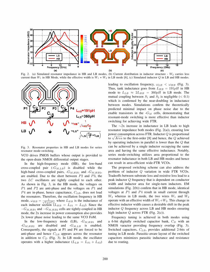
Fig. 2. (a) Simulated resonator impedance in HB and LB modes, (b) Current distribution in inductor structure - W2 carries lesscurrent than W1 in HB Mode, while the effective width is W1 + W2 in LB mode [6], (c) Simulated inductor Q in LB and HB modes.
Fig. 3. Resonator properties in HB and LB modes for seriesresonator mode-switching.VCO drives PMOS buffers whose output is provided tothe open-drain NMOS differential output stages.
In the high-frequency mode (HB), the low-bandcross-coupled pair (-GM,LB) is disabled while thehigh-band cross-coupled pairs, -GM,HB1 and -GM,HB2,are enabled. Due to the short between P2 and P3, thetwo LC oscillators are tightly coupled to each other.As shown in Fig. 3, in the HB mode, the voltages onP1 and P2 are anti-phase and the voltages on P1 andP4 are in-phase, hence capacitance, CLB , does not loadthe resonators. Therefore, the oscillation frequency in HBmode, ωHB = 1√
LHBCDwhere LHB is the inductance of
each inductor section (LHB = LS1 = LS2). Since the−GM,HB1 and −GM,HB2 cells are tightly-coupled in HBmode, the 2x increase in power consumption also provides2x lower phase noise leading to the same VCO FoM.
In the low-frequency mode (LB), -GM,HB1 and-GM,HB2 are disabled and -GM,LB is enabled.Consequently, the signals at P1 and P4 are forced to beanti-phase and hence CLB appears across the resonatorin addition to CD (Fig. 3). In LB mode, the oscillatoroperates with a higher inductance (LLB = LS1 + LS2)
leading to oscillation frequency, ωLB < ωHB (Fig. 3).Thus, tank inductance goes from LHB = 191pH in HBmode to LLB ≈ 2LHB = 360pH in LB mode. Themutual coupling between S1 and S2 is negligible (< 0.1)which is confirmed by the near-doubling in inductancebetween modes. Simulations confirm the theoreticallypredicted minimal impact on phase noise due to theenable transistors in the -GM cells, demonstrating thatresonant-mode switching is more effective than inductorswitching for achieving wide FTR.
The ∼2x increase in inductance in LB leads to highresonator impedance both modes (Fig. 2(a)), ensuring lowpower consumption across FTR. Inductor Q is proportionalto√Area to the first-order [8] and hence, the Q achieved
by operating inductors in parallel is lower than the Q thatcan be achieved by a single inductor occupying the samearea and having the same effective inductance. Notably,series mode-switching utilizes area proportional to theresonator inductance in both LB and HB modes and hencecan result in area-efficient wide-FTR VCOs.
The proposed switching scheme can also address theproblem of inductor Q variation in wide FTR VCOs.Tradeoffs between substrate loss and resistive loss lead to apeak inductor Q frequency that is dependent on conductorwidth and inductor area for single-turn inductors. EMsimulations (Fig. 2(b)) confirm that in HB mode, identicalvoltages at P1 and P4 result in small current throughW2 whereas in LB mode, the two wires W1 and W2
operate with an effective width of W1+W2. This change ineffective inductor width causes a desirable shift in the peakinductor Q frequency across LB and HB modes ensuringhigh inductor Q across FTR (Fig. 2(c)).
Frequency tuning is achieved in both modes usinga 6-bit digitally switched capacitor bank, CD with anNMOS varactor providing frequency overlap (Fig. 3).Switched capacitors, CLB , provides additional 2-bits oftuning in LB mode. Parasitic-aware layout of the switchedcapacitors minimizes parasitic inductance and resistancedue to routing.
200
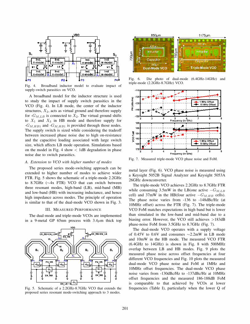
Fig. 4. Broadband inductor model to evaluate impact ofsupply-switch parasitics on VCO.
A broadband model for the inductor structure is usedto study the impact of supply switch parasitics in theVCO (Fig. 4). In LB mode, the center of the inductorstructures, X2, acts as virtual ground and therefore supplyfor -GM,LB is connected to X2. The virtual ground shiftsto X1 and X3 in HB mode and therefore supply for-GM,HB1 and -GM,HB1 is provided through those nodes.The supply switch is sized while considering the tradeoffbetween increased phase noise due to high on-resistanceand the capacitive loading associated with large switchsize, which affects LB mode operation. Simulations basedon the model in Fig. 4 show < 1dB degradation in phasenoise due to switch parasitics.
A. Extension to VCO with higher number of modes
The proposed series mode-switching approach can beextended to higher number of modes to achieve widerFTR. Fig. 5 shows the schematic of a triple-mode 2.2GHzto 8.7GHz (∼4x FTR) VCO that can switch betweenthree resonant modes, high-band (LB), mid-band (MB)and low-band (HB) with increasing inductance, and hencehigh impedance across modes. The principle of operationis similar to that of the dual-mode VCO shown in Fig. 3.
III. MEASURED PERFORMANCE
The dual-mode and triple-mode VCOs are implementedin a 9-metal GP 65nm process with 3.4µm thick top
Fig. 5. Schematic of a 2.2GHz-8.7GHz VCO that extends theproposed series resonant mode-switching approach to 3 modes.
Fig. 6. Die photo of dual-mode (6.4GHz-14GHz) andtriple-mode (2.2GHz-8.7GHz) VCO.
Fig. 7. Measured triple-mode VCO phase noise and FoM.
metal layer (Fig. 6). VCO phase noise is measured usinga Keysight 5052B Signal Analyzer and Keysight 5053A26GHz downconverter.
The triple-mode VCO achieves 2.2GHz to 8.7GHz FTRwhile consuming 3.5mW in the LB(one active −GM,LB
cell) and 37mW in the HB(four active −GM,HB cells).The phase noise varies from -136 to -148dBc/Hz (at10MHz offset) across the FTR (Fig. 7). The triple-modeVCO FoM matches expectations in high band but is lowerthan simulated in the low-band and mid-band due to abiasing error. However, the VCO still achieves >183dBphase-noise FoM from 3.5GHz to 8.7GHz (Fig. 7).
The dual-mode VCO operates with a supply voltageof 0.45V to 0.6V and consumes ∼2.2mW in LB modeand 10mW in the HB mode. The measured VCO FTR(6.4GHz to 14GHz) is shown in Fig. 8 with 500MHzoverlap between LB and HB modes. Fig. 9 plots themeasured phase noise across offset frequencies at fourdifferent VCO frequencies and Fig. 10 plots the measureddual-mode VCO phase noise and FoM at 1MHz and10MHz offset frequencies. The dual-mode VCO phasenoise varies from -130dBc/Hz to -137dBc/Hz at 10MHzoffset frequencies and the measured 186-188dB FoMis comparable to that achieved by VCOs at lowerfrequencies (Table I), particularly when the lower Q of
201
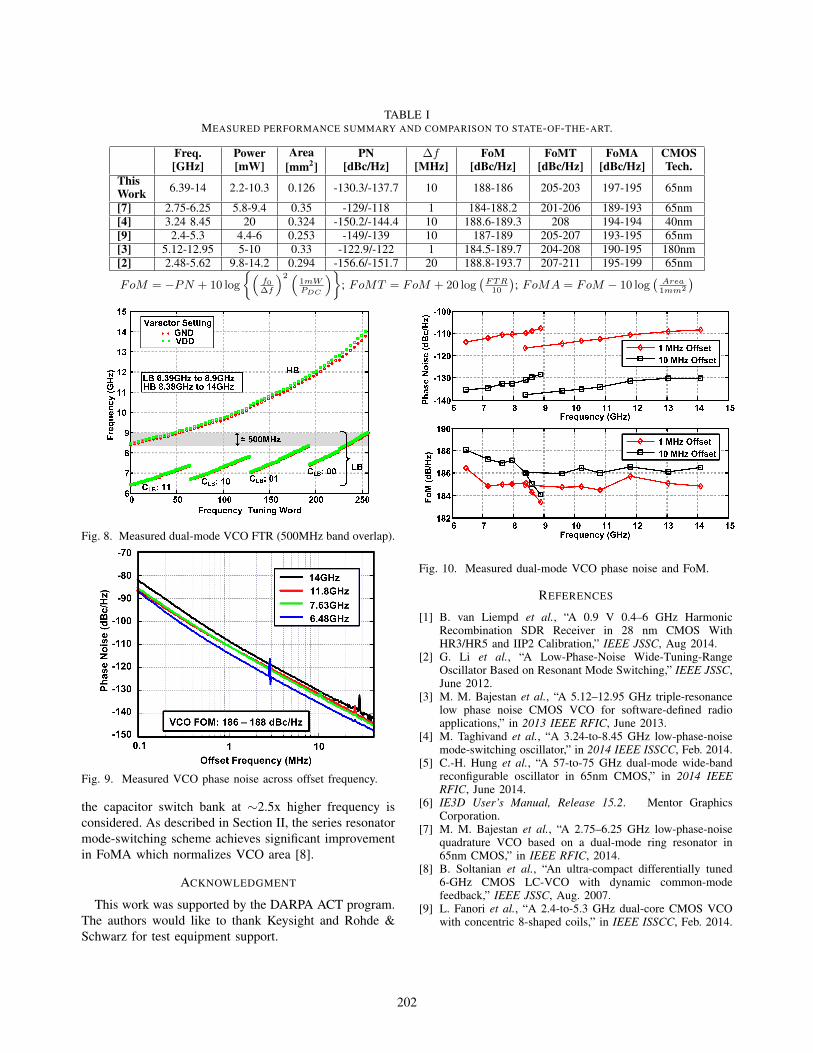
TABLE IMEASURED PERFORMANCE SUMMARY AND COMPARISON TO STATE-OF-THE-ART.
Freq.[GHz]
Power[mW]
Area[mm2]
PN[dBc/Hz]
∆f[MHz]
FoM[dBc/Hz]
FoMT[dBc/Hz]
FoMA[dBc/Hz]
CMOSTech.
ThisWork 6.39-14 2.2-10.3 0.126 -130.3/-137.7 10 188-186 205-203 197-195 65nm
[7] 2.75-6.25 5.8-9.4 0.35 -129/-118 1 184-188.2 201-206 189-193 65nm[4] 3.24 8.45 20 0.324 -150.2/-144.4 10 188.6-189.3 208 194-194 40nm[9] 2.4-5.3 4.4-6 0.253 -149/-139 10 187-189 205-207 193-195 65nm[3] 5.12-12.95 5-10 0.33 -122.9/-122 1 184.5-189.7 204-208 190-195 180nm[2] 2.48-5.62 9.8-14.2 0.294 -156.6/-151.7 20 188.8-193.7 207-211 195-199 65nm
FoM = −PN + 10 log
{(f0∆f
)2 (1mWPDC
)}; FoMT = FoM + 20 log
(FTR
10
); FoMA = FoM − 10 log
(Area1mm2
)
Fig. 8. Measured dual-mode VCO FTR (500MHz band overlap).
Fig. 9. Measured VCO phase noise across offset frequency.
the capacitor switch bank at ∼2.5x higher frequency isconsidered. As described in Section II, the series resonatormode-switching scheme achieves significant improvementin FoMA which normalizes VCO area [8].
ACKNOWLEDGMENT
This work was supported by the DARPA ACT program.The authors would like to thank Keysight and Rohde &Schwarz for test equipment support.
Fig. 10. Measured dual-mode VCO phase noise and FoM.
REFERENCES
[1] B. van Liempd et al., “A 0.9 V 0.4–6 GHz HarmonicRecombination SDR Receiver in 28 nm CMOS WithHR3/HR5 and IIP2 Calibration,” IEEE JSSC, Aug 2014.
[2] G. Li et al., “A Low-Phase-Noise Wide-Tuning-RangeOscillator Based on Resonant Mode Switching,” IEEE JSSC,June 2012.
[3] M. M. Bajestan et al., “A 5.12–12.95 GHz triple-resonancelow phase noise CMOS VCO for software-defined radioapplications,” in 2013 IEEE RFIC, June 2013.
[4] M. Taghivand et al., “A 3.24-to-8.45 GHz low-phase-noisemode-switching oscillator,” in 2014 IEEE ISSCC, Feb. 2014.
[5] C.-H. Hung et al., “A 57-to-75 GHz dual-mode wide-bandreconfigurable oscillator in 65nm CMOS,” in 2014 IEEERFIC, June 2014.
[6] IE3D User’s Manual, Release 15.2. Mentor GraphicsCorporation.
[7] M. M. Bajestan et al., “A 2.75–6.25 GHz low-phase-noisequadrature VCO based on a dual-mode ring resonator in65nm CMOS,” in IEEE RFIC, 2014.
[8] B. Soltanian et al., “An ultra-compact differentially tuned6-GHz CMOS LC-VCO with dynamic common-modefeedback,” IEEE JSSC, Aug. 2007.
[9] L. Fanori et al., “A 2.4-to-5.3 GHz dual-core CMOS VCOwith concentric 8-shaped coils,” in IEEE ISSCC, Feb. 2014.
202