Embed Size (px)
Citation preview
MEE 1413: Electronics Power Conversion Dr. Zainal Salam; Dec 2000
1
ELECTRONICS POWER CONVERSION
INTRODUCTION
• Definition and concepts of Electronics Power Conversion
• Application
• Power semiconductor switches
• Gate/base drivers
• Losses
• Snubbers
• Links to useful websites
• Reading material:– Mohan (Chapter)
– Bose paper
MEE 1413: Electronics Power Conversion Dr. Zainal Salam; Dec 2000
2
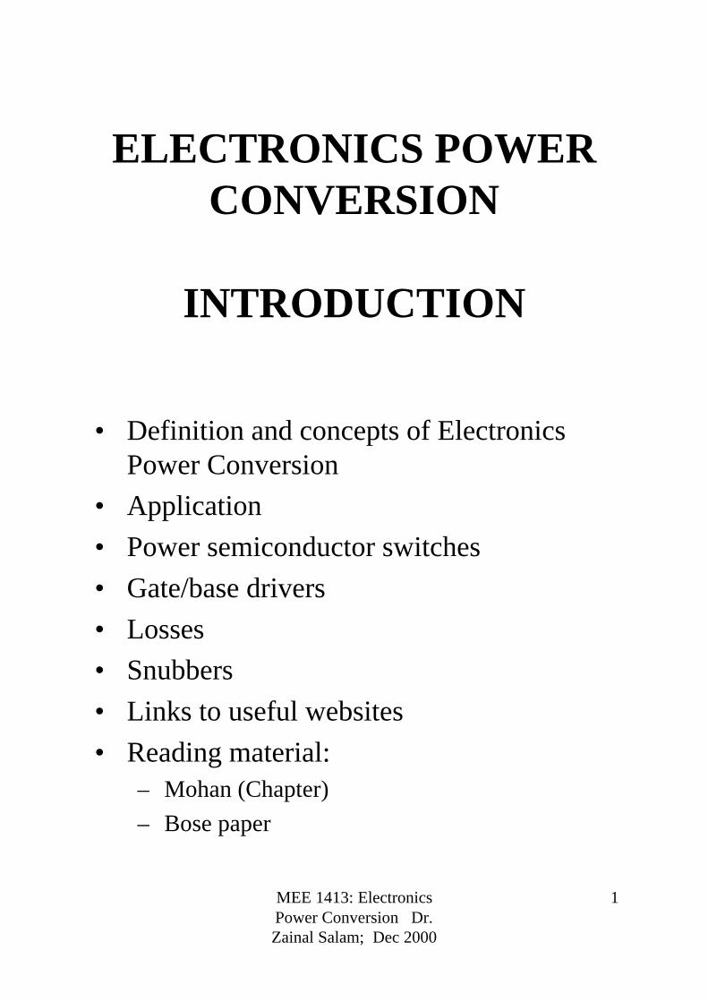
ELECTRONIC POWER CONVERSION
• DEFINITION: To convert, i.e to processand control the flow of electric power by supplying voltage s and currents in a form that is optimally suited for user loads.
• More popularly known as “power electronics” (PE) systems. Basic block diagram shown in Figure 1.
Power Processor
Controller
Load
measurement
reference
POWERINPUT
POWEROUTPUT
vi , ii vo , io
Figure 1

MEE 1413: Electronics Power Conversion Dr. Zainal Salam; Dec 2000
3
Goal of electronic power conversion systems
• To convert electrical energy from one form to another, from the source to load with highest efficiency, high availability and high reliability with the lowest cost, smallest size and weight.
• Static and applications– involves non-rotating or moving mechanical
components.
– E.g rectifiers, inverters, choppers, cycloconverters.
• Drive applications– intimately contains moving or rotating
components such as motors.
– E.g. DC drives, AC drives, Permanent magnet motor drives.

MEE 1413: Electronics Power Conversion Dr. Zainal Salam; Dec 2000
4
Conversion concept: example
• Supply from TNB: 50Hz, 240V RMS (340V peak). Customer need DC voltage for welding purpose, say.
• TNB sine-wave supply gives zero DC component!
• We can use simple half-wave rectifier. A fixed DC voltage is now obtained. This is a simple PE system.
time
VTNB (Volt)
Vo
time
Vdc
+Vo
_
+VTNB
_
πm
oV
V =
:tageoutput vol Average
MEE 1413: Electronics Power Conversion Dr. Zainal Salam; Dec 2000
5
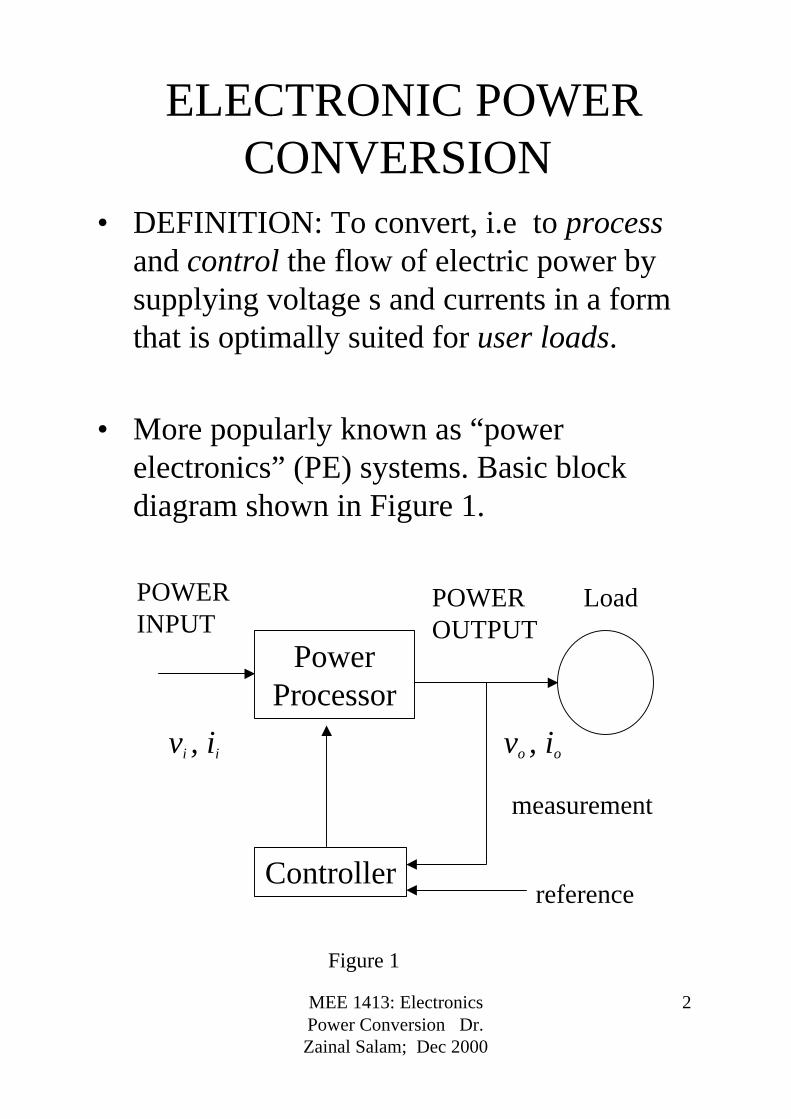
Concept-cont’d
+vo
_
+vs
_
ig
ia
ωt
vs
voia
α
ig
α
ωt
( ) [ ]απ
ωωπ
π
α
cos12
sin21
:tageoutput vol Average
+== ∫ mmo
VtdtVV
How if customer wants variable DC voltage?More complex circuit using SCR is required.
By controlling the firing angle, α,the output DC voltage (after conversion) can be varied..
Obviously this needs a complicated electronic system to set the firing current pulses for the SCR.

MEE 1413: Electronics Power Conversion Dr. Zainal Salam; Dec 2000
6
Applications
• Power generation and transmission (HVDC)
• Uninterruptable power supplies (UPS)
• DC power supplies
• Energy conservation (ballast, pumps, compressors, air-condition)
• Transportation (Electric car, trains)
• Process control and factory automation
• Electroplating, Welding
• Heating,cooling
• Utility-related application
MEE 1413: Electronics Power Conversion Dr. Zainal Salam; Dec 2000
7
Current issues related to power electronics: Energy scenario
• Energy Scenario.– Need to reduce dependence on fossil fuel (coal,
natural gas, oil) and nuclear power resource (uranium).
– Depletion of these sources is expected (see Bose paper).
– Effort to tap renewable energy resources such as solar, wind, fuel-cell etc. need to be increased.
– Energy saving: 15-20% of electricity can be saved by PE applications.
– E.g. variable speed drives (air conditioned, fans, pumps). Variable speed compressor aircond system saves up to 30% of energy compared to conventional thermostat-controlled system.
– electrical lighting using electronics ballast can boost the efficiency of fluorescent lamp by 20%.

MEE 1413: Electronics Power Conversion Dr. Zainal Salam; Dec 2000
8
Environmental issues
• Environment issues– Nuclear safety. Nuclear plants can remain
radioactive for thousands of years.
– Burning of fossil fuel emits gases such as CO2, CO (oil burning), SO2, NOX (coal burning) etc.
– Creates global warming (green house effect), acid rain and urban pollution from smokes.
– One way to reduce the problem is to promote renewable energy resources.
– To mitigate the pollution problem, centralization of power stations to remote non-urban are needed. Stringent controls can be imposed on central power plants.
– Special effort is needed to reduce pollution in cities by enforcing the use of electric vehicle.
MEE 1413: Electronics Power Conversion Dr. Zainal Salam; Dec 2000
9
PE growth
• PE rapid growth due to: – Advances in power (semiconductor) switches
– Advances in microelectronics (DSP, VLSI, microprocessor/microcontroller, ASIC)
– New ideas in control algorithms
– Demand for new applications
• PE is an interdisciplinary field:– Digital/analogue electronics
– Power and energy
– Microelectronics
– Control system
– Computer, simulation and software
– Solid-state physics and devices
– Packaging
– Heat transfer
MEE 1413: Electronics Power Conversion Dr. Zainal Salam; Dec 2000
10
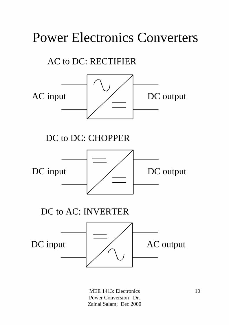
Power Electronics Converters
AC input DC output
DC input AC output
AC to DC: RECTIFIER
DC to DC: CHOPPER
DC to AC: INVERTER
DC input DC output

MEE 1413: Electronics Power Conversion Dr. Zainal Salam; Dec 2000
11
Application example:Static converter
FILTER LOADDC-DCCONVERTER
DIODERECTIFIER
AC voltage
AC LINEVOLTAGE(1 or 3 )Φ Φ
Vcontrol(derived from
feedback circuit)
EMIFILTER
RECTIFIERAND
FILTER
HighFrequency
rectifierandfilter
Base/gatedrive
PWMController
errorAmp
Vo
Vref
DCRegulated
DC-DC CONVERSITION + ISOLATION
DCUnregulated
Switched-mode power supply
DC to DC converter

MEE 1413: Electronics Power Conversion Dr. Zainal Salam; Dec 2000
12
Application example:Variable speed drive system
Controller PowerElectronicsConverter
ProcessControl
Computer
Motor Process/Load
Power Source
SystemController
PowerElectronicsConverter
Motor Airconditioner
Power Source
BuildingCooling
Desiredtemperature
Indoorsensors
Indoor temperatureand humidity
Temperature andhumidity
Desiredhumidity
Variable speed drive
Air-conditioning system
MEE 1413: Electronics Power Conversion Dr. Zainal Salam; Dec 2000
13
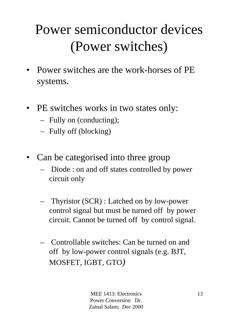
Power semiconductor devices (Power switches)
• Power switches are the work-horses of PE systems.
• PE switches works in two states only: – Fully on (conducting);
– Fully off (blocking)
• Can be categorised into three group– Diode : on and off states controlled by power
circuit only
– Thyristor (SCR) : Latched on by low-power control signal but must be turned off by power circuit. Cannot be turned off by control signal.
– Controllable switches: Can be turned on and off by low-power control signals (e.g. BJT,
MOSFET, IGBT, GTO)

MEE 1413: Electronics Power Conversion Dr. Zainal Salam; Dec 2000
14
Power Diode
• When diode is forward biased, it conducts current with a small forward voltage (Vf) across it (0.2-3V)
• When reversed (or blocking state), a negligibly small leakage current (uA to mA) flows until the reverse breakdown occurs. Diode should not be operated at reverse voltage greater than Vr
Id
VdVf
Vr
A (Anode)
K (Cathode)
+Vd
_Id
Diode: Symbol v-i characteristics
MEE 1413: Electronics Power Conversion Dr. Zainal Salam; Dec 2000
15
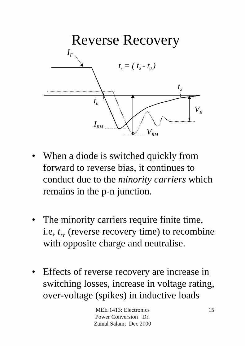
Reverse Recovery
• When a diode is switched quickly from forward to reverse bias, it continues to conduct due to the minority carriers which remains in the p-n junction.
• The minority carriers require finite time, i.e, trr (reverse recovery time) to recombine with opposite charge and neutralise.
• Effects of reverse recovery are increase in switching losses, increase in voltage rating, over-voltage (spikes) in inductive loads
IF
IRM
VR
t0
t2
trr= ( t2 - t0 )
VRM

MEE 1413: Electronics Power Conversion Dr. Zainal Salam; Dec 2000
16
Softness factor, Sr
IF
VR
t0
t2
Sr= ( t2 - t1 )/(t1 - t0)
= 0.8
t1
IF
VR
t0
Sr= ( t2 - t1 )/(t1 - t0)
= 0.3
t1 t2
Snap-off
Soft-recovery

MEE 1413: Electronics Power Conversion Dr. Zainal Salam; Dec 2000
17
Types of Power Diodes
• Line frequency (general purpose): – on state voltage very low (below 1V)
– large trr (about 25us)
– very high current (up to 5kA) and voltage (5kV) ratings
– Used in line-frequency (50/60Hz) applications such as rectifiers
• Fast recovery– very low trr (<1us).
– Power levels at several hundred volts and several hundred amps
– Normally used in high frequency circuits
• Schottky– very low forward voltage drop (typical 0.3V)
– limited blocking voltage (50-100V)
– Used in low voltage, high current application such as switched mode power supplies.

MEE 1413: Electronics Power Conversion Dr. Zainal Salam; Dec 2000
18
Thyristor (SCR)
• Thyristors can only be turned on with two conditions:– the device is in forward blocking state (i.e Vak is
positive)
– a positive gate current (Ig) is applied at the gate
• Once conducting, the anode current is LATCHED (continuously flowing).
Ia
Vak
Vr
Ig=0Ig>0Ih
Ibo
v-i characteristics
A (Anode)
K (Cathode)
+Vak
_
Ia
Thyristor: Symbol
G (Gate)
Ig
Vbo

MEE 1413: Electronics Power Conversion Dr. Zainal Salam; Dec 2000
19
Turning on/off mechanism• In reverse -biased mode, the SCR behaves
like a diode. It conducts a small leakage current which is almost dependent of the voltage, but increases with temperature.
• When the peak reverse voltage is exceeded, avalanche breakdown occurs, and the large current will flow.
• In the forward biased mode, with no gate current present (i.e. in the untriggered state, the device exhibits a leakage current.
• If the forward breakover voltage (Vbo) is exceeded, the SCR “self-triggers” into the conducting state and and the voltage collapses to the normal forward volt-drop, typically 1.5-3V. The presence of any gate current will reduce the forward breakover voltage.

MEE 1413: Electronics Power Conversion Dr. Zainal Salam; Dec 2000
20
Thyristor Conduction
• Thyristor cannot be turned off by applying negative gate current. It can only be turned off if Ia goes negative (reverse)– This happens when negative portion of the of
sine-wave occurs (natural commutation),
• Another method of turning off is known as “forced commutation”,– The anode current is “diverted” to another
circuitry.
+vs
_
iak
+vo
_
+ vak -
ig
ωt
vs
voia
α
ig
α
ωt
MEE 1413: Electronics Power Conversion Dr. Zainal Salam; Dec 2000
21
Types of thyristors• Phase controlled
– rectifying line frequency voltage and current for ac and dc motor drives
– large voltage (up to 7kV) and current (up to 4kA) capability
– low on-state voltage drop (1.5 to 3V)
• Inverter grade– used in inverter and chopper
– Quite fast. Can be turned-on using “force-commutation” method.
• Light activated – Similar to phase controlled, but triggered by
pulse of light.
– Normally very high power ratings
• TRIAC– Dual polarity thyristors
MEE 1413: Electronics Power Conversion Dr. Zainal Salam; Dec 2000
22
Controllable switches (power transistors)
• Can be turned “ON”and “OFF” by relatively very small control signals.
• Operated in SATURATION and CUT-OFF modes only. No “linear region” operation is allowed due to excessive power loss.
• In general, power transistors do not operate in latched mode.
• Traditional devices: Bipolar junction transistors (BJT), Metal oxide silicon field effect transistor ( MOSFET), Insulated gate bipolar transistors (IGBT), Gate turn-off thyristors (GTO)
• Emerging (new) devices: Gate controlled thyristors (GCT).

MEE 1413: Electronics Power Conversion Dr. Zainal Salam; Dec 2000
23
Bipolar Junction Transistor (BJT)
• Ratings: Voltage: VCE<1000, Current: IC<400A. Switching frequency up to 5kHz. Low on-state voltage: VCE(sat) : 2-3V
• Low current gain (β). Need high base current to obtain reasonable IC . Expensive and complex base drive circuit.
• Not popular in new products.
IC
VCE
IB
v-i characteristics
VCE (sat)
BJT: symbol (npn)
+VCE
_
IC
IB
C (collector)
B (base)
E (emitter)
MEE 1413: Electronics Power Conversion Dr. Zainal Salam; Dec 2000
24
BJT characteristics
• To turn on/off the device, a base drive circuit is connected to the base and emitter terminal.
• To turn on, current is injected into the base terminal. When turned on, conventional current passes from collector to emitter.
• To turn-off, the base current is removed.
• The current gain of a BJT ends to be low when operated in the saturated ON condition. β<10 is common. It deteriorates as voltage ratings increases.
• It is normal to use Darlington connection for higher current gain.

MEE 1413: Electronics Power Conversion Dr. Zainal Salam; Dec 2000
25
BJT Darlington pair
+VCE
_
IC2
IB2
C (collector)
E (emitter)
IC
IB1
B (base)
IC1Driver Transistor Output
Transistor
Biasing/ stabilising network
( )
( )
2121
121
1
1121
1
2
2
21
1
2
1
11211
1
βββββ
βββ
βββ
β
++=⇒
+⋅+=
+⋅+=
⋅
+=
+=+==
B
cB
B
B
B
c
B
c
B
cBccBc
I
II
I
I
I
II
I
I
IIIIII

MEE 1413: Electronics Power Conversion Dr. Zainal Salam; Dec 2000
26
Metal Oxide Silicon Field Effect Transistor (MOSFET)
• Ratings: Voltage VDS<500V, current IDS<300A.
• Very fast device: >100KHz. For some low power devices (few hundred watts) may go up to MHz range.
ID
VDS
v-i characteristicsMOSFET: symbol
(n-channel)
+VDS
_
ID
D (drain)
G (gate)
S (source)
+VGS
_
+VGS
_

MEE 1413: Electronics Power Conversion Dr. Zainal Salam; Dec 2000
27
MOSFET characteristics• Turning on and off is very simple. Only
need to provide VGS =+15V to turn on and 0V to turn off. Gate drive circuit is simple.
• Basically low voltage device. High voltage device are available up to 600V but with limited current. Can be paralleled quite easily for higher current capability.
• Internal (dynamic) resistance between drain and source during on state, RDS(ON), , limits the power handling capability of MOSFET. High losses especially for high voltage device due to RDS(ON) .
• Dominant in high frequency application (>100kHz). Biggest application is in switched-mode power supplies.

MEE 1413: Electronics Power Conversion Dr. Zainal Salam; Dec 2000
28
Insulated Gate Bipolar Transistor (IGBT)
• Combination of BJT and MOSFET characteristics. Compromises include:
– Gate behaviour similar to MOSFET - easy to turn on and off.
– Low losses like BJT due to low on-state Collector-Emitter voltage (2-3V).
IC
VCE
VGE
v-i characteristics
VCE (sat)
IGBT: symbol
+VCE
_
IC
C (collector)
G (gate)
E (emitter)
+VGE _

MEE 1413: Electronics Power Conversion Dr. Zainal Salam; Dec 2000
29
IGBT
• Ratings: Voltage: VCE<3.3kV, Current,: IC<1.2kA currently available. Work in under progress for 4.5kV/1.2kA device. Constant improvement in voltage and current ratings
• Good switching capability (up to 100KHz) for newer devices. Typical application, IGBT is used at 20-50KHz.
• For very high power devices and applications, frequency is limited to several KHz.
• Very popular in new products; practically replacing BJT in most new applications.
• “Snubberless” operation is possible. Most new IGBTs do not require snubbers.

MEE 1413: Electronics Power Conversion Dr. Zainal Salam; Dec 2000
30
Gate turn-off thyristor (GTO)
• Behave like normal thyristor, but can be turned off using gate signal
• However turning off is difficult. Need very large reverse gate current (normally 1/5 of anode current)
G (Gate)
Ia
Vak
Vr
Ig=0Ig>0Ih
Ibo
v-i characteristics
A (Anode)
K (Cathode)
+Vak
_
Ia
GTO: Symbol
Ig

MEE 1413: Electronics Power Conversion Dr. Zainal Salam; Dec 2000
31
GTO
• Ratings: Voltage: Vak<5kV; Current: Ia<5kA. Highest power ratings switch. Frequency<5KHz.
• Gate drive design is very difficult. Need very large reverse gate current to turn off. Often custom-tailored to specific application.
• Currently getting very stiff competition from high power IGBT. The latter has much simpler and cheaper drivers.
• GTO normally requires snubbers. High power snubbers are expensive.
• In very high power region (>5kV, >5kA), development in gate-controlled thyristor (GCT) may effectively end the future of GTO

MEE 1413: Electronics Power Conversion Dr. Zainal Salam; Dec 2000
32
(Base/gate) Driver circuit
• Interface between control (low power electronics) and (high power) switch. Functions:– amplifies control signal to a level required to
drive power switch
– provides electrical isolation between power
switch and logic level
• Complexity of driver varies markedly among switches. MOSFET/IGBT drivers are simple but GTO drivers are very complicated and expensive.
Control
Circuit
Driver
Circuit
Powerswitch
MEE 1413: Electronics Power Conversion Dr. Zainal Salam; Dec 2000
33
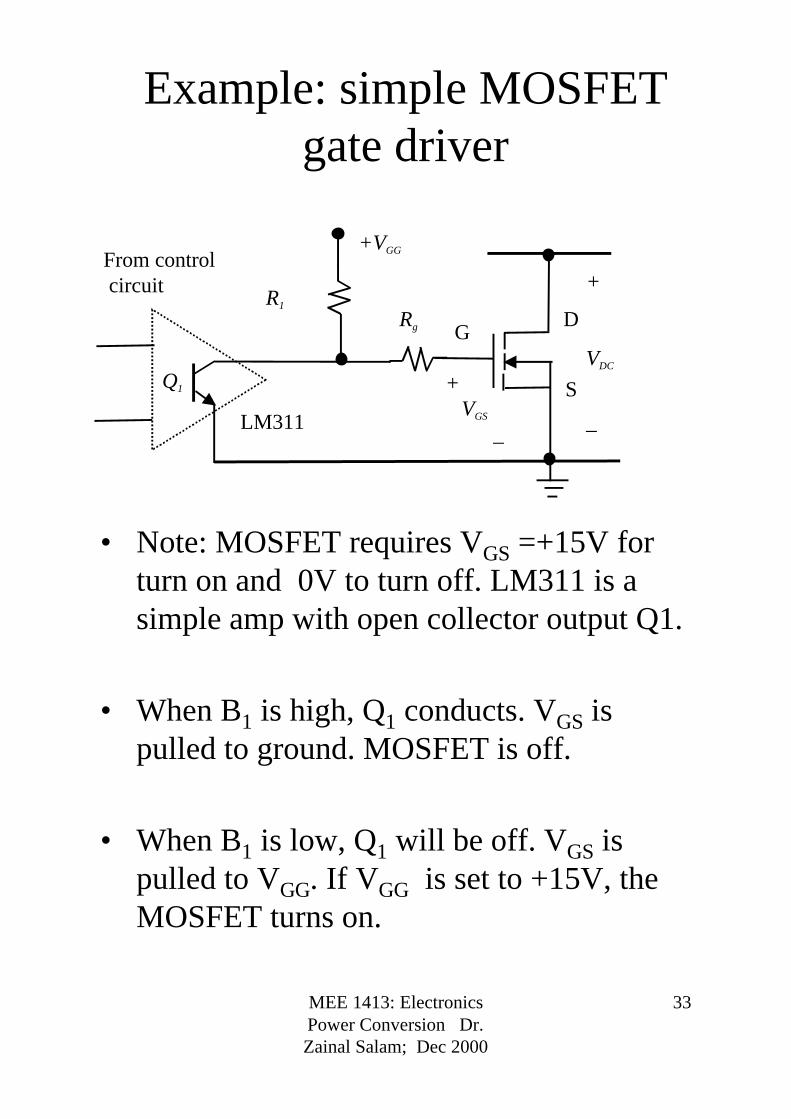
Example: simple MOSFET gate driver
• Note: MOSFET requires VGS =+15V for turn on and 0V to turn off. LM311 is a simple amp with open collector output Q1.
• When B1 is high, Q1 conducts. VGS is pulled to ground. MOSFET is off.
• When B1 is low, Q1 will be off. VGS is pulled to VGG. If VGG is set to +15V, the MOSFET turns on.
+
VDC
_
DG
S+VGS
_
From controlcircuit
+VGG
R1
Rg
LM311
Q1

MEE 1413: Electronics Power Conversion Dr. Zainal Salam; Dec 2000
34
Gate drive for thyristors
• Pulse transformer is used for isolation. R1 is to limit the gate current
• Normally a pulse with length 10us with amplitude of 50mA is sufficient to turn-on the thyristors.It is quite common to fire the thyristors with successive pulses to ensure proper turn-on.
• It is not possible to turn-off a thyristor with the above circuit
+
vak-
iak
Pulse source
igR1
R2
Pulse transformer

MEE 1413: Electronics Power Conversion Dr. Zainal Salam; Dec 2000
35
Electrical isolation for drivers
• Isolation is required to prevent damages on the high power switch to propagate back to low power electronics.
• Normally opto-coupler (shown below) or high frequency magnetic materials (as shown in the thyristor case) are used.
• Many standard driver chips have built-in isolation. For example TLP 250 from Toshiba, HP 3150 from Hewlett-Packard uses opto-coupling isolation.
From controlcircuit To driverQ1 D1 A1
Opto-coupler isolation

MEE 1413: Electronics Power Conversion Dr. Zainal Salam; Dec 2000
36
Switches comparisons (2000)
Thy BJT FET GTO IGBT
Avail-abilty
Early60s
Late 70s Early80s
Mid 80s Late80s
State ofTech.
Mature Mature Mature/improve
Mature Rapidimprove
Voltageratings
5kV 1kV 500V 5kV 3.3kV
Currentratings
4kA 400A 200A 5kA 1.2kA
SwitchFreq.
na 5kHz 1MHz 2kHz 100kHz
On-stateVoltage
2V 1-2V I* Rds(on)
2-3V 2-3V
DriveCircuit
Simple Difficult Verysimple
Verydifficult
Verysimple
Comm-ents
Cannotturnoffusinggatesignals
Phasingout innewproduct
Goodperformance inhighfreq.
King inveryhighpower
Bestoverallperformance.

MEE 1413: Electronics Power Conversion Dr. Zainal Salam; Dec 2000
37
Application examples
• For each of the following application, choose the best power switches and reason out why.
– An inverter for the light-rail train (LRT) locomotive operating from a DC supply of 750 V. The locomotive is rated at 150 kW. The induction motor is to run from standstill up to 200 Hz, with power switches frequencies up to 10KHz.
– A switch-mode power supply (SMPS) for remote telecommunication equipment is to be developed. The input voltage is obtained from a photovoltaic array that produces a maximum output voltage of 100 V and a minimum current of 200 A. The switching frequency should be higher than 100kHz.
– A HVDC transmission system transmitting power of 300 MW from one ac system to another ac system both operating at 50 Hz, 230 kV rms line to line and the DC link voltage operating at 200 kV.

MEE 1413: Electronics Power Conversion Dr. Zainal Salam; Dec 2000
38
Power switch losses
• It is important to consider losses of power switches:– to ensure that the system operates reliably under
prescribed ambient conditions
– so that heat removal mechanism (e.g. heat sink, radiators, coolant) can be specified. Heat sinks and other heat removal systems are costly and bulky.
– losses in switches affects the system efficiency
• If a power switch is not cooled to its specified junction temperature, the full power capability of the switch cannot be realised. Derating of the power switch ratings may be necessary.
• Main losses occurs in power switches are – forward conduction losses,
– blocking state losses
– switching losses

MEE 1413: Electronics Power Conversion Dr. Zainal Salam; Dec 2000
39
Forward conduction losses
• Ideal switch has zero voltage drop across it during turn-on (Von). Although the forward current ( Ion ) may be large, the losses on the switch is zero.
• But for real switches, e.g. BJT, IGBT, GTO, SCR, GCT have forward conduction voltage (on state) between 1-3V. MOSFET has on state voltage which is characterised by the RDS(ON).
+Von−
Ion
Ideal switch
Ion +Von−
Real switch

MEE 1413: Electronics Power Conversion Dr. Zainal Salam; Dec 2000
40
Forward conduction and blocking state losses
• Losses is measured by product of volt-drop across the device Von with the current, Ion, averaged over the period.
• Forward conduction losses is the major source of loss at low frequency and DC operation.
• During turn-off, the switch blocks large voltage. Ideally no current should flow through the switch. But for real switch a small amount of leakage current may flow. This creates turn-off or blocking state losses
• The leakage current during turn-off is normally very small, Hence the turn-off losses are usually neglected.

MEE 1413: Electronics Power Conversion Dr. Zainal Salam; Dec 2000
41
Switching losses
• During turn-on and turn off, ideal switch requires zero transition time. Voltage and current are switched instantaneously.
• In real switch,due to the non-idealities of power switches, the switching profile is as shown in above.
• The switching losses occurs as a result of both the voltage and current changing simultaneously during the switching period.
vi
time
Ideal switching profile(turn on)
v i
time
Real switching profile(turn-on)
P=vi
Energy
MEE 1413: Electronics Power Conversion Dr. Zainal Salam; Dec 2000
42
Switching losses• The product of device voltage and current
gives instantaneous power dissipated in the device.
• The heat energy that developed over the switching period is the integration (summation) of instantaneous power over time as shown by the shaded area under the power curve.
• The average power loss is the sum of the turn-on and turn off energies multiplied by the switching frequency.
• When frequency increase, switching losses increases. This limits the usable range of power switches unless proper heat removal mechanism is employed.

MEE 1413: Electronics Power Conversion Dr. Zainal Salam; Dec 2000
43
Safe Operating Area (SOA)• Convenient method to summarise
maximum values of current and voltage to which the power switch should be subjected;
• Different devices have different SOA. Example of SOA for a typical BJT is shown below.
VCE (Volt)
0.1
100
10
200
1.0
300
0.1 10010 2001.0 300
100ms10ms 1ms
10us
100us
I C(A
mp)

MEE 1413: Electronics Power Conversion Dr. Zainal Salam; Dec 2000
44
Snubbers
• PCB construction, wire loops creates stray inductance, Ls.
• Using KVL,
time
Vce
Vce rated
+Vin
−
Ls
+Vce
−
+VL−
i
dt
diLvv
dtdidt
diLvv
vdt
diLvvv
since
since
cescesin
+=
−=
+=+=
off) (turning negative is since
Simple switch at turn off

MEE 1413: Electronics Power Conversion Dr. Zainal Salam; Dec 2000
45
Snubbers• From previous equation, the voltage across
the switch is bigger than the supply (for a short moment).
• The spike may exceed the switch rated blocking voltage and causes damage due to overvoltage.
• To prevent such occurrence, a snubber is put across the switch. An example of a snubber is an RCD circuit shown below.
• Snubber circuit “smoothened” the transition and make the switch voltage rise more “slowly”. In effect it dampens the high voltage spike to a safe value.
• Switches and diodes requires snubbers. However, new generation of IGBT, MOSFET and GCT do not require it.

MEE 1413: Electronics Power Conversion Dr. Zainal Salam; Dec 2000
46
RCD Snubbers
• In general, snubbers are used for:
– turn-on: to minimise large overcurrents through the device at turn-on
– turn-off: to minimise large overvoltages across the device during turn-off.
– Stress reduction: to shape the device switching waveform such that the voltage and current associated with the device are not high simultaneously.
+Vce
−
Ls
time
Vce
Vce rated
MEE 1413: Electronics Power Conversion Dr. Zainal Salam; Dec 2000
47
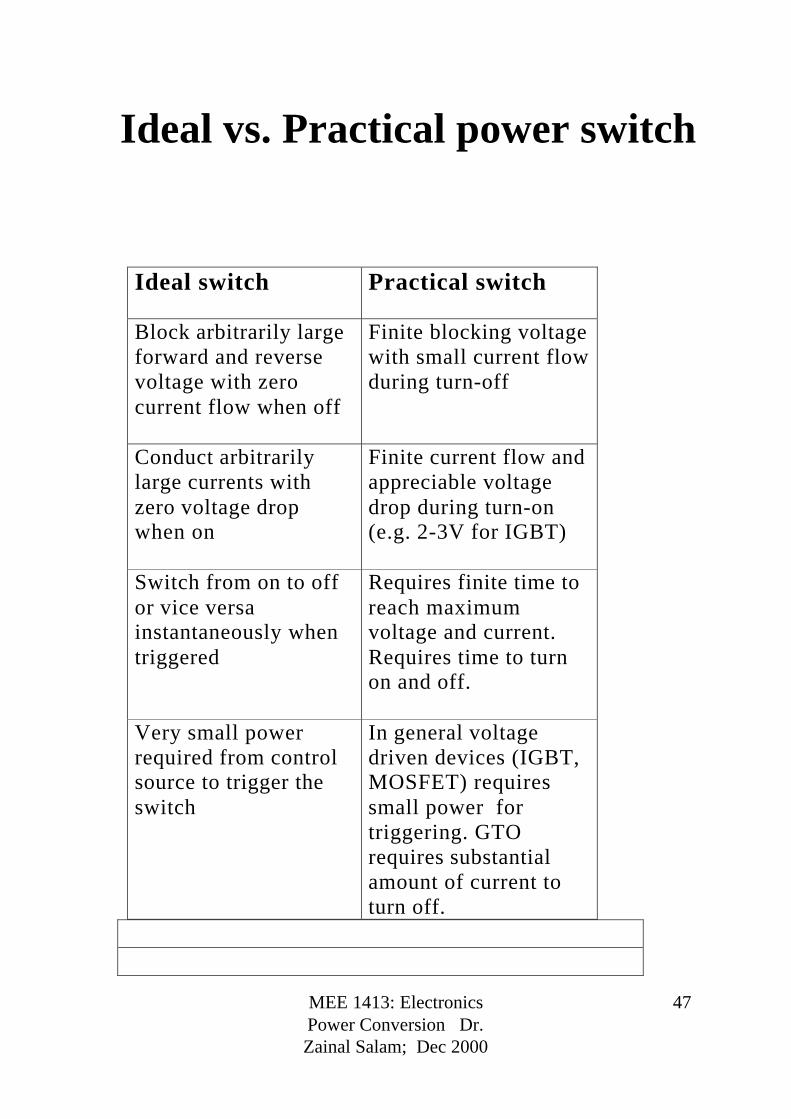
Ideal vs. Practical power switch
Ideal switch Practical switch
Block arbitrarily largeforward and reversevoltage with zerocurrent flow when off
Finite blocking voltagewith small current flowduring turn-off
Conduct arbitrarilylarge currents withzero voltage dropwhen on
Finite current flow andappreciable voltagedrop during turn-on(e.g. 2-3V for IGBT)
Switch from on to offor vice versainstantaneously whentriggered
Requires finite time toreach maximumvoltage and current.Requires time to turnon and off.
Very small powerrequired from controlsource to trigger theswitch
In general voltagedriven devices (IGBT,MOSFET) requiressmall power fortriggering. GTOrequires substantialamount of current toturn off.

MEE 1413: Electronics Power Conversion Dr. Zainal Salam; Dec 2000
48
Related websites for further readings/info/data sheet.
• Power switches– power diodes (irf.com) (semikron.com)
– thyristors (irf.com) (semikron.com)
– IGBT (siemens.com) (irf.com) (toshiba.com),
– MOSFETS (irf.com)
– GTO (abb.com)
– GCT (abb.com)
• Drivers– IGBT (toshiba.com), (hp.com) (semikron.com)
• Complete power electronics solutions– (abb.com)