Embed Size (px)
Citation preview
Electronics Imaging System for
the Synchrotron Light Source
Walter Y. Mok
Alan Fisher, Weixing Chen, Jeff Corbett
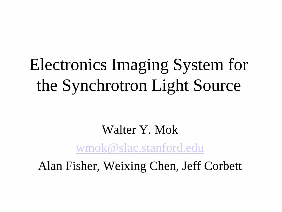
The key components of an Electronic Imaging
System for a synchrotron light source
Light collection /
Relay Optics
Image / light
Processing
Optics
Camera
Optics
Sensor
Read out Electronics
Interface to
the computer
Frame
Grabber
Digital Image
Processing
Software
Display
and
storage
Electronic
Camera
Computer
Image
Processing
Computer
DisplayVideo
Display
Control Electronics
Optics
Light Source
Key components of an electronic imaging system
• The source – what is coming out of the Synchrotron?
• The optics – to transform the light from the source for detection
• The camera – to detect the transformed light
• Digital image processing – to extract and store information
Visible Beam Source
Characterization
• Vertical beam size – Interferometer, CCD camera
• Cross section /vertical / horizontal– CCD camera
• Axial beam size – temporal beam size, Streak
camera.
• Time history of the beam – Scanning mirror
imaging system, amplitude variation over time
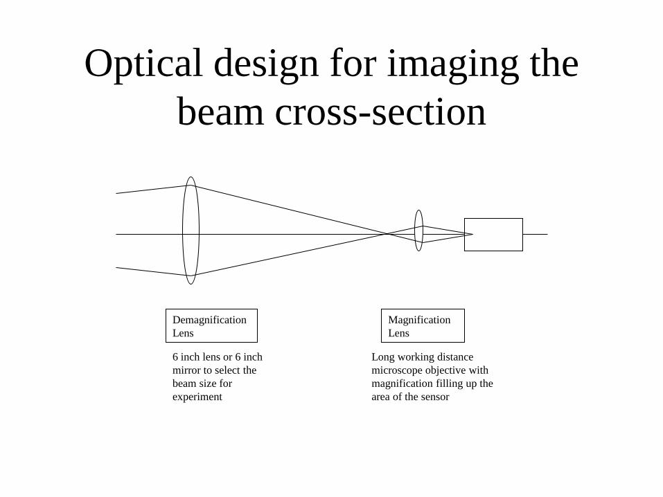
Optical design for imaging the
beam cross-section
Demagnification
Lens
Magnification
Lens
Long working distance
microscope objective with
magnification filling up the
area of the sensor
6 inch lens or 6 inch
mirror to select the
beam size for
experiment
Optical design
• Polarization change due to reflection –variation of the X- and Y-components of the
• Wave front deterioration causing variation in beam size
• Reflective optics – advantage, wide band, spherical aberation, focal length varies with aperture
• Refractive optics – chromatic aberration, variation in focus for different color of light
Speed
• Processing time
• Rise time- 10, 300 ps, 5 ns
• Fall time - ns
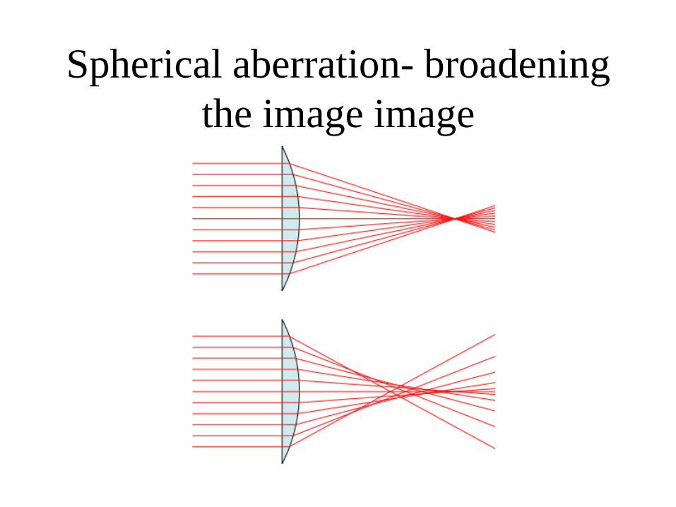
Spherical aberration- broadening
the image image
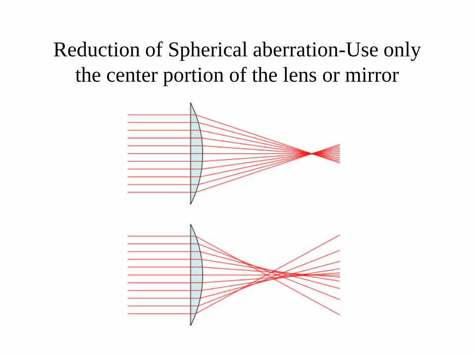
Reduction of Spherical aberration-Use only
the center portion of the lens or mirror
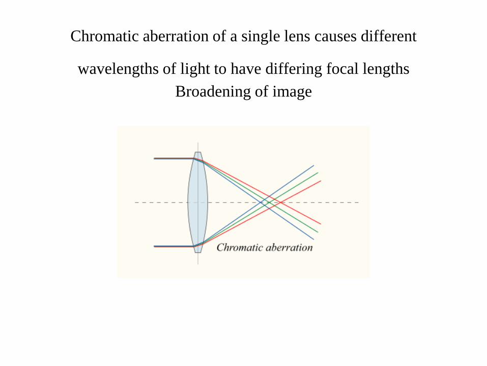
Chromatic aberration of a single lens causes different
wavelengths of light to have differing focal lengths
Broadening of image
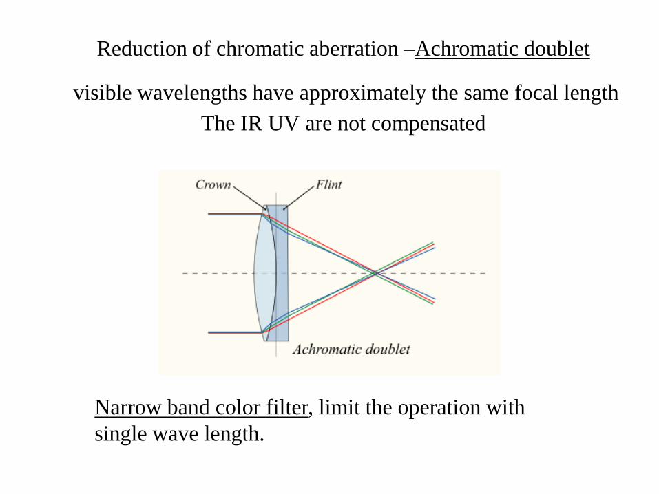
Reduction of chromatic aberration –Achromatic doublet
visible wavelengths have approximately the same focal length
The IR UV are not compensated
Narrow band color filter, limit the operation with
single wave length.
PI-MAX Data Acquisition
• Major components of the Intensified-CCD
• PI-Max Data Acquisition system
• Operation of PI-Max Data Acquisition
system
• Application in synchrotron light imaging.
Different Kinds of Imaging Sensors
• CCD – Charge Coupled Device
• ICCD – Intensified CCD
• EMCCD – Electron Multiplying CCD
• CMOS – Complementary Metal Oxide
Semiconductor
How is CCD different from CMOS ?
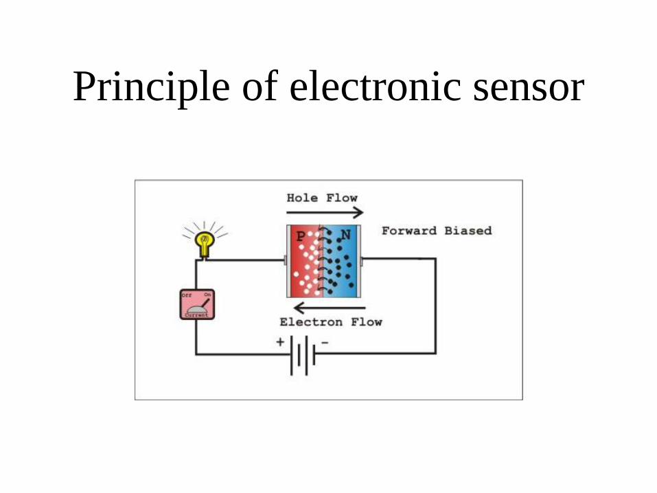
Principle of electronic sensor

CCD 2-Dimension array
Choosing a sensor• Spectral response
– Energy band gap
– Silicon 1.15 ev fro vis UV and nir
– Germanium for IR
• Window material
– Quartz – UV transmission
– AR coating : VIS
– BK7 glass: UV Fluoresce
– Germanium: for IR
• Substrate thickness
– 7 -10 micron for soft x-ray
– 3 micron for back illumination, high speed
• CCD IR, VIS, UV, Soft X-ray
Sensitivity
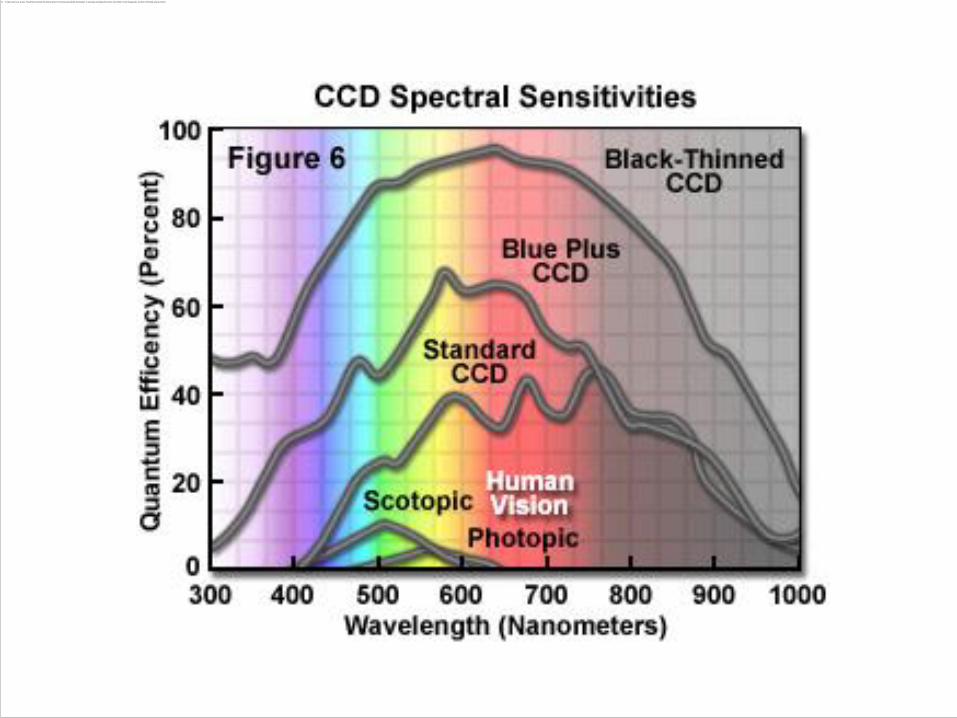
• Quantum efficiency – number of charges generated per
photon as a function of wave length in %
• Dynamic Range – response to weak and strong light
• Linearity – Out put voltage as function of the intensity of
the light
• Resolution –
– Number of pixel, 1600 X 1200, 640 X 480, 2048 X 1536,
– 2592 X 1944, 3072 X 2304
– Pixel size
– Geometry of the pixel size, square pixel
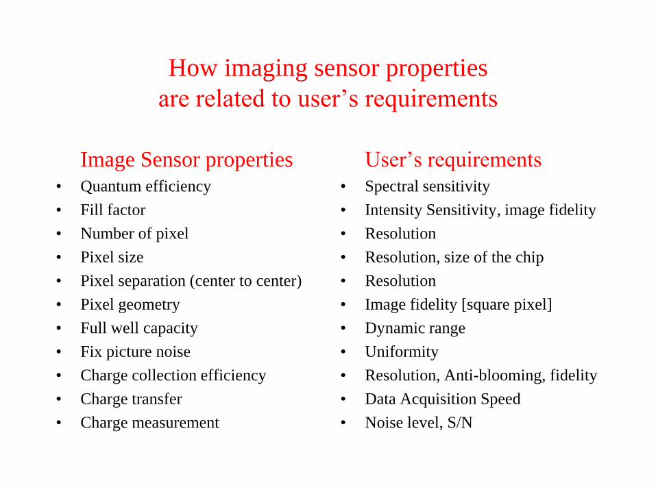
How imaging sensor properties
are related to user’s requirements
Image Sensor properties
• Quantum efficiency
• Fill factor
• Number of pixel
• Pixel size
• Pixel separation (center to center)
• Pixel geometry
• Full well capacity
• Fix picture noise
• Charge collection efficiency
• Charge transfer
• Charge measurement
User’s requirements
• Spectral sensitivity
• Intensity Sensitivity, image fidelity
• Resolution
• Resolution, size of the chip
• Resolution
• Image fidelity [square pixel]
• Dynamic range
• Uniformity
• Resolution, Anti-blooming, fidelity
• Data Acquisition Speed
• Noise level, S/N
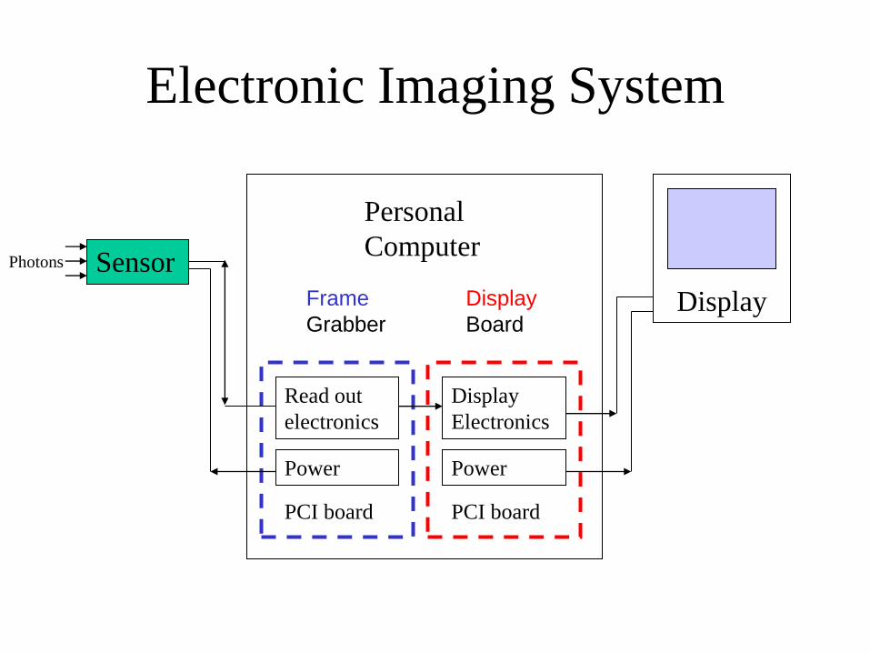
Electronic Imaging System
Sensor
Power
Read out
electronics
Display
Electronics
Power
Display
PCI board
Frame
Grabber
Display
Board
PCI board
Personal
ComputerPhotons
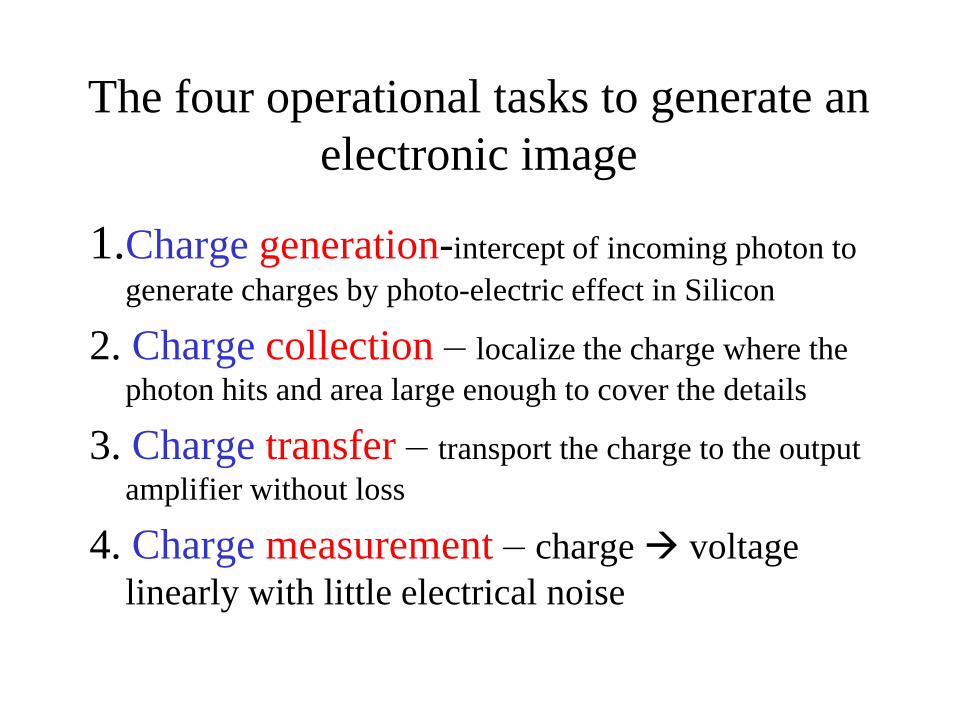
The four operational tasks to generate an
electronic image
1.Charge generation-intercept of incoming photon to
generate charges by photo-electric effect in Silicon
2. Charge collection – localize the charge where the
photon hits and area large enough to cover the details
3. Charge transfer – transport the charge to the output
amplifier without loss
4. Charge measurement – charge voltage
linearly with little electrical noise
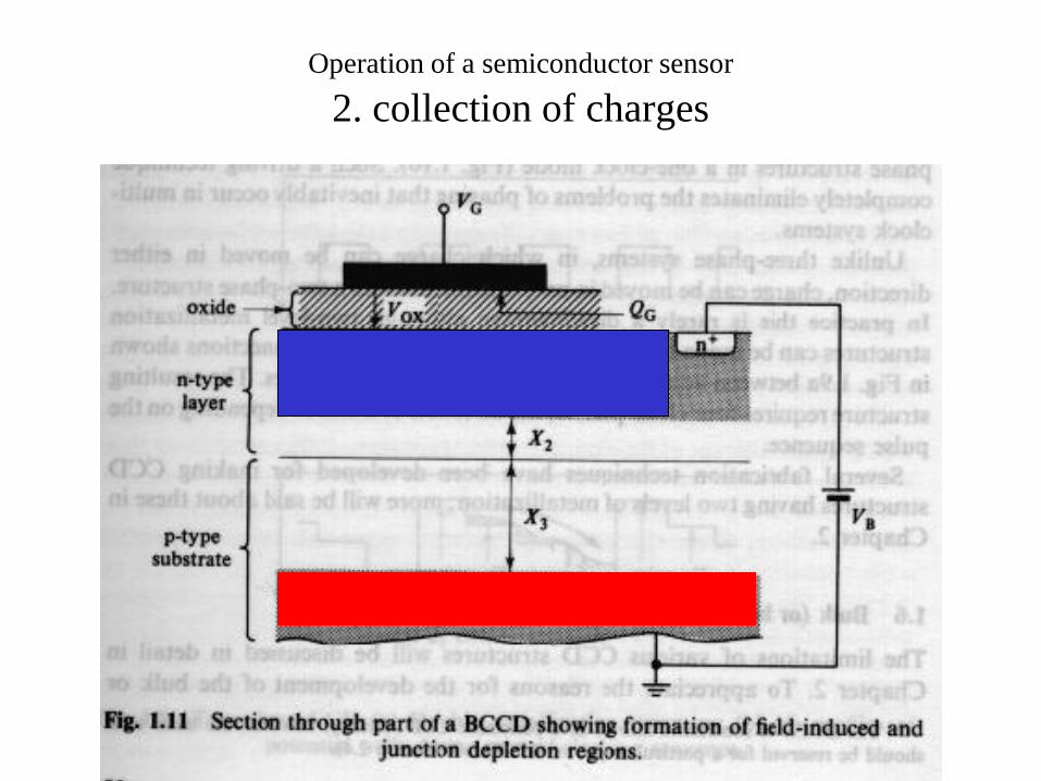
Operation of a semiconductor sensor
2. collection of charges
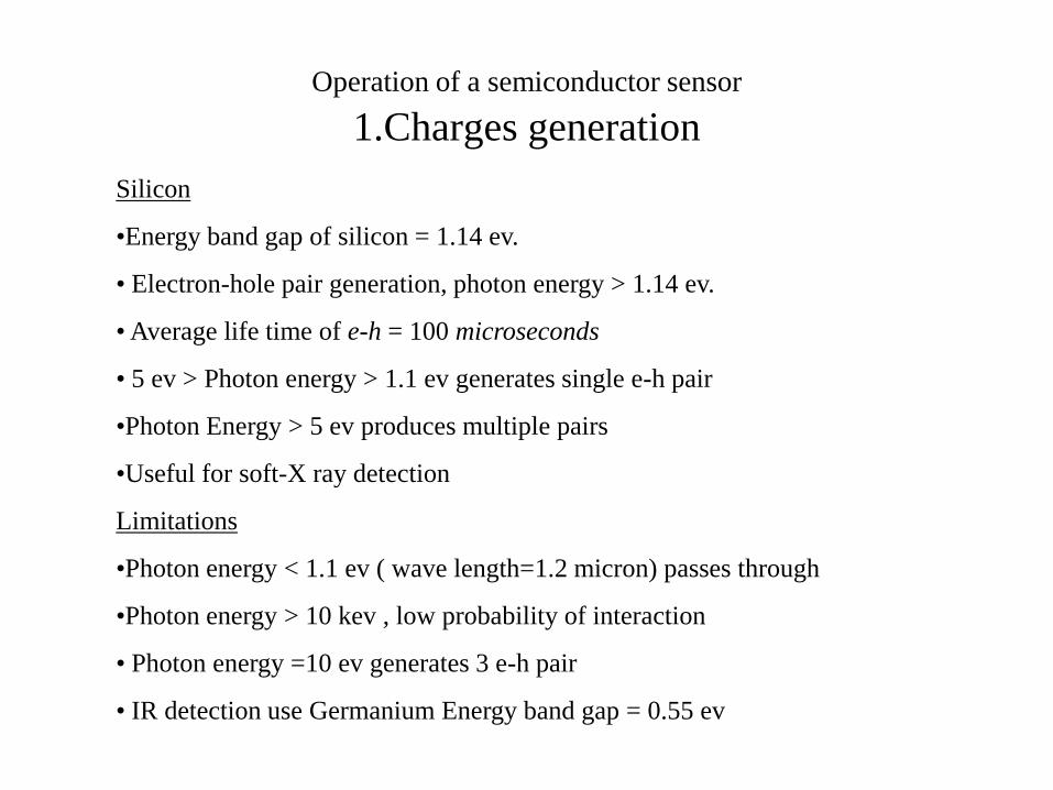
Operation of a semiconductor sensor
1.Charges generation
Silicon
•Energy band gap of silicon = 1.14 ev.
• Electron-hole pair generation, photon energy > 1.14 ev.
• Average life time of e-h = 100 microseconds
• 5 ev > Photon energy > 1.1 ev generates single e-h pair
•Photon Energy > 5 ev produces multiple pairs
•Useful for soft-X ray detection
Limitations
•Photon energy < 1.1 ev ( wave length=1.2 micron) passes through
•Photon energy > 10 kev , low probability of interaction
• Photon energy =10 ev generates 3 e-h pair
• IR detection use Germanium Energy band gap = 0.55 ev
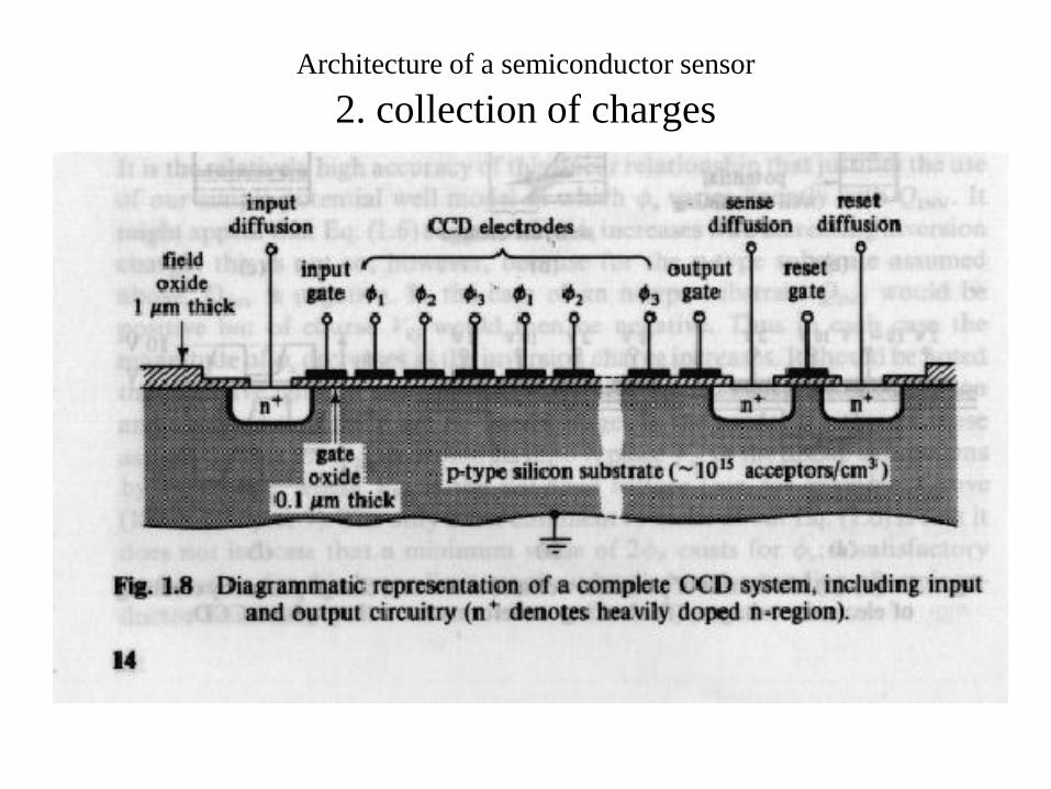
Architecture of a semiconductor sensor
2. collection of charges
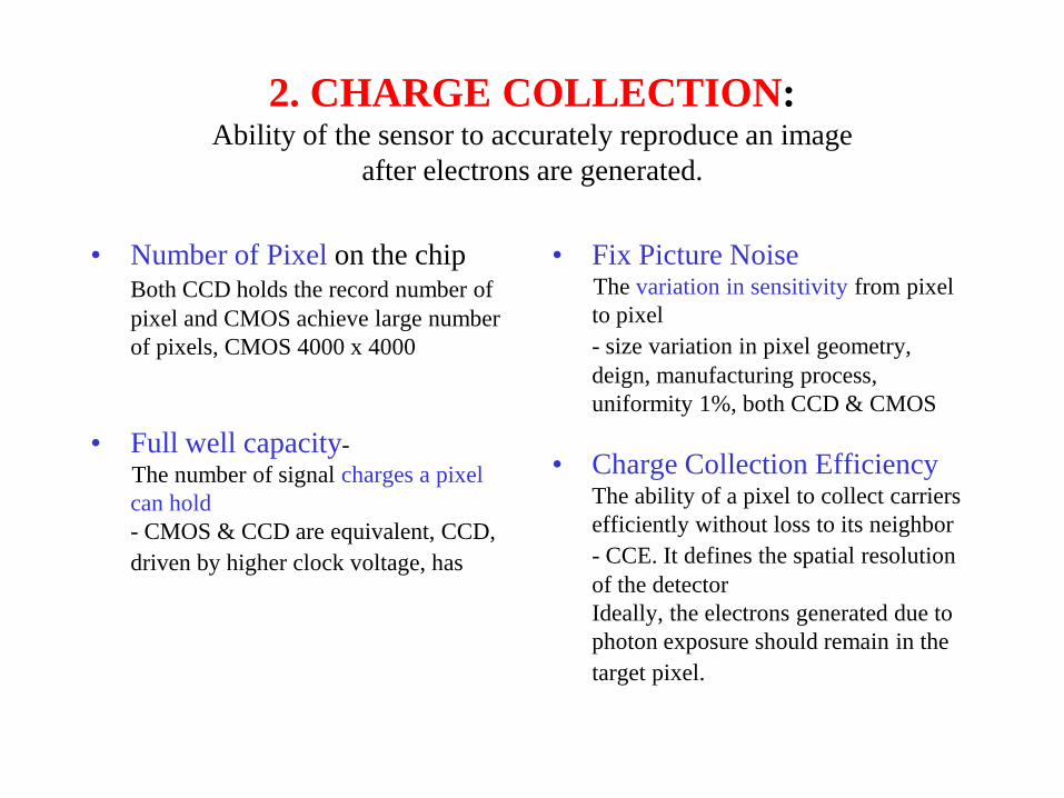
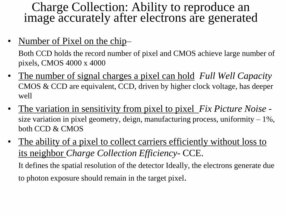
2. CHARGE COLLECTION: Ability of the sensor to accurately reproduce an image
after electrons are generated.
• Number of Pixel on the chipBoth CCD holds the record number of
pixel and CMOS achieve large number
of pixels, CMOS 4000 x 4000
• Full well capacity-
The number of signal charges a pixel
can hold
- CMOS & CCD are equivalent, CCD,
driven by higher clock voltage, has
• Fix Picture NoiseThe variation in sensitivity from pixel
to pixel
- size variation in pixel geometry,
deign, manufacturing process,
uniformity 1%, both CCD & CMOS
• Charge Collection EfficiencyThe ability of a pixel to collect carriers
efficiently without loss to its neighbor
- CCE. It defines the spatial resolution
of the detector
Ideally, the electrons generated due to
photon exposure should remain in the
target pixel.
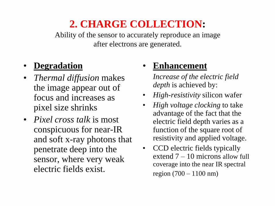
2. CHARGE COLLECTION: Ability of the sensor to accurately reproduce an image
after electrons are generated.
• Degradation
• Thermal diffusion makes the image appear out of focus and increases as pixel size shrinks
• Pixel cross talk is most conspicuous for near-IR and soft x-ray photons that penetrate deep into the sensor, where very weak electric fields exist.
• Enhancement
Increase of the electric field depth is achieved by:
• High-resistivity silicon wafer
• High voltage clocking to take advantage of the fact that the electric field depth varies as a function of the square root of resistivity and applied voltage.
• CCD electric fields typically extend 7 – 10 microns allow full coverage into the near IR spectral
region (700 – 1100 nm)
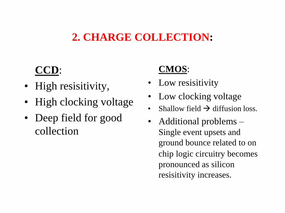
2. CHARGE COLLECTION:
CCD:
• High resisitivity,
• High clocking voltage
• Deep field for good
collection
CMOS:
• Low resisitivity
• Low clocking voltage
• Shallow field diffusion loss.
• Additional problems –Single event upsets and
ground bounce related to on
chip logic circuitry becomes
pronounced as silicon
resisitivity increases.
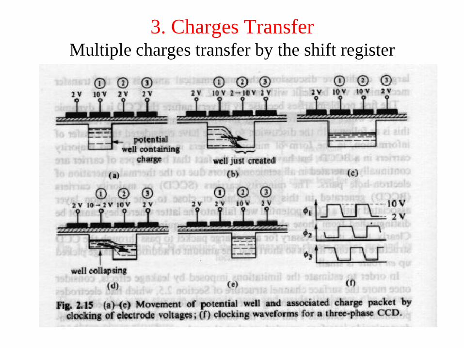
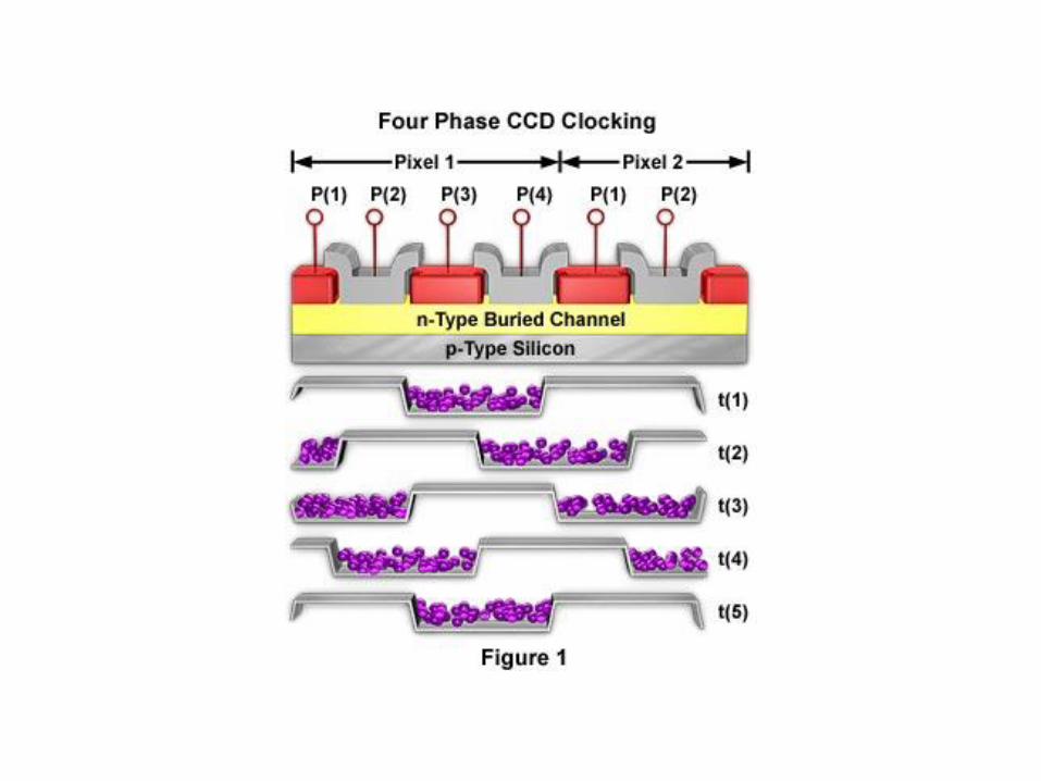
3. Charges TransferMultiple charges transfer by the shift register
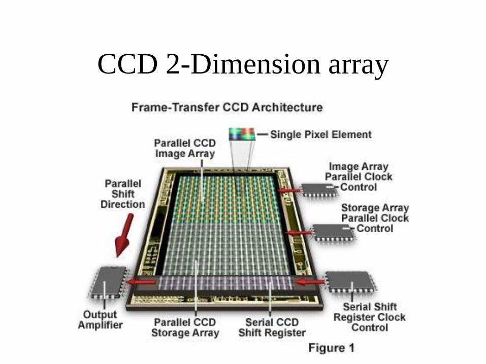
CCD 2-Dimension array
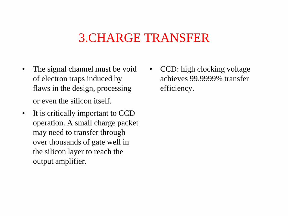
3.CHARGE TRANSFER
• The signal channel must be void
of electron traps induced by
flaws in the design, processing
or even the silicon itself.
• It is critically important to CCD
operation. A small charge packet
may need to transfer through
over thousands of gate well in
the silicon layer to reach the
output amplifier.
• CCD: high clocking voltage
achieves 99.9999% transfer
efficiency.

http://learn.hamamatsu.com/tutorials/fourphase/
Operation of a semiconductor sensor
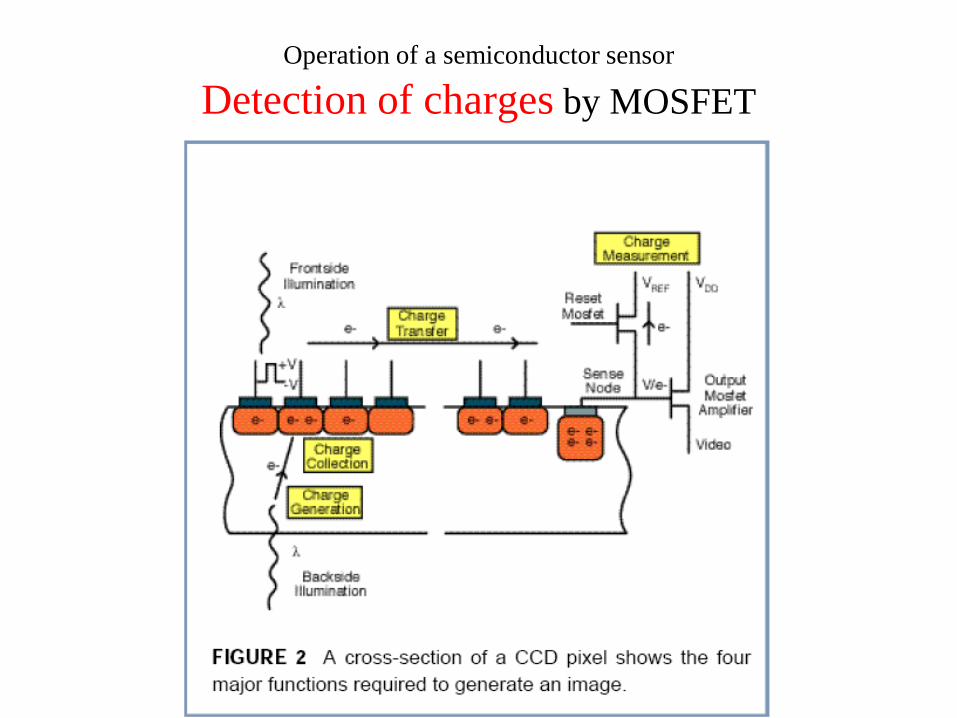
Detection of charges by MOSFET
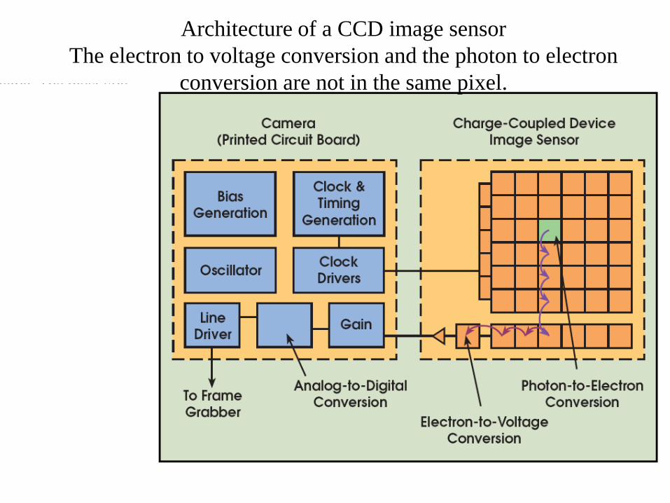
Architecture of a CCD image sensor
The electron to voltage conversion and the photon to electron
conversion are not in the same pixel.
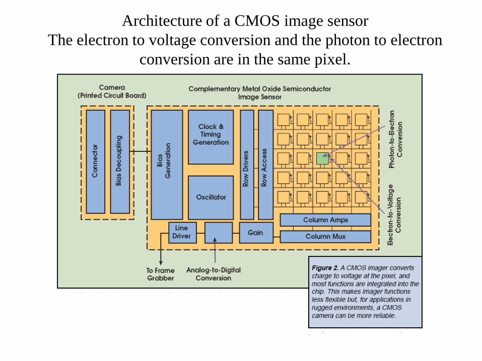
Architecture of a CMOS image sensor
The electron to voltage conversion and the photon to electron
conversion are in the same pixel.
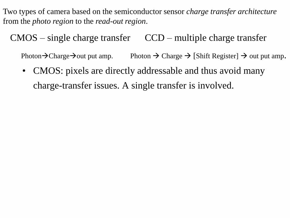
Two types of camera based on the semiconductor sensor charge transfer architecture
from the photo region to the read-out region.
CMOS – single charge transfer CCD – multiple charge transfer
PhotonChargeout put amp. Photon Charge [Shift Register] out put amp.
• CMOS: pixels are directly addressable and thus avoid many
charge-transfer issues. A single transfer is involved.
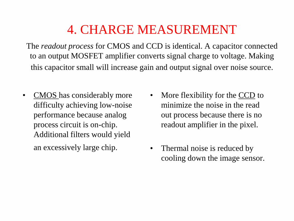
4. CHARGE MEASUREMENTThe readout process for CMOS and CCD is identical. A capacitor connected
to an output MOSFET amplifier converts signal charge to voltage. Making
this capacitor small will increase gain and output signal over noise source.
• CMOS has considerably more
difficulty achieving low-noise
performance because analog
process circuit is on-chip.
Additional filters would yield
an excessively large chip.
• More flexibility for the CCD to
minimize the noise in the read
out process because there is no
readout amplifier in the pixel.
• Thermal noise is reduced by
cooling down the image sensor.
Charge Collection: Ability to reproduce an image accurately after electrons are generated
• Number of Pixel on the chip–
Both CCD holds the record number of pixel and CMOS achieve large number of
pixels, CMOS 4000 x 4000
• The number of signal charges a pixel can hold Full Well CapacityCMOS & CCD are equivalent, CCD, driven by higher clock voltage, has deeper
well
• The variation in sensitivity from pixel to pixel Fix Picture Noise -size variation in pixel geometry, deign, manufacturing process, uniformity – 1%,
both CCD & CMOS
• The ability of a pixel to collect carriers efficiently without loss to
its neighbor Charge Collection Efficiency- CCE.
It defines the spatial resolution of the detector Ideally, the electrons generate due
to photon exposure should remain in the target pixel.
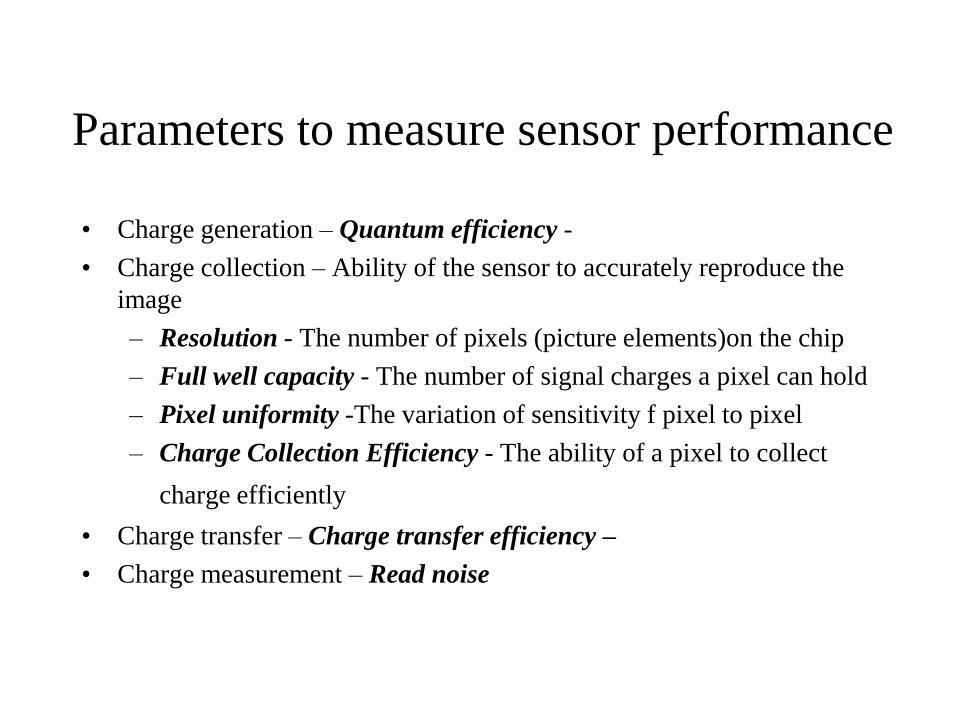
Parameters to measure sensor performance
• Charge generation – Quantum efficiency -
• Charge collection – Ability of the sensor to accurately reproduce the
image
– Resolution - The number of pixels (picture elements)on the chip
– Full well capacity - The number of signal charges a pixel can hold
– Pixel uniformity -The variation of sensitivity f pixel to pixel
– Charge Collection Efficiency - The ability of a pixel to collect
charge efficiently
• Charge transfer – Charge transfer efficiency –
• Charge measurement – Read noise
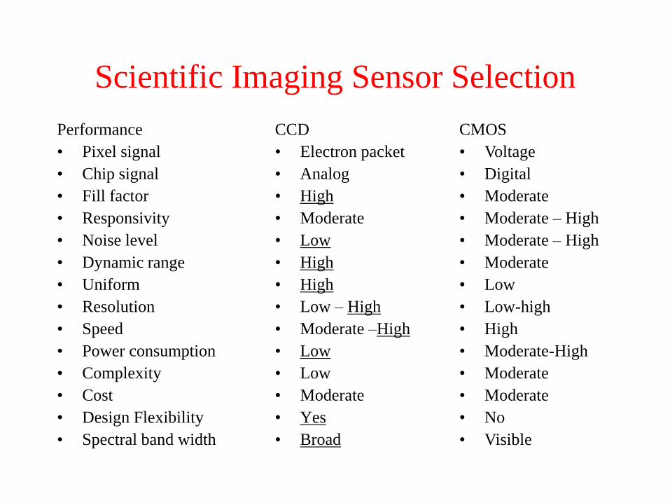
Scientific Imaging Sensor Selection
Performance
• Pixel signal
• Chip signal
• Fill factor
• Responsivity
• Noise level
• Dynamic range
• Uniform
• Resolution
• Speed
• Power consumption
• Complexity
• Cost
• Design Flexibility
• Spectral band width
CCD
• Electron packet
• Analog
• High
• Moderate
• Low
• High
• High
• Low – High
• Moderate –High
• Low
• Low
• Moderate
• Yes
• Broad
CMOS
• Voltage
• Digital
• Moderate
• Moderate – High
• Moderate – High
• Moderate
• Low
• Low-high
• High
• Moderate-High
• Moderate
• Moderate
• No
• Visible
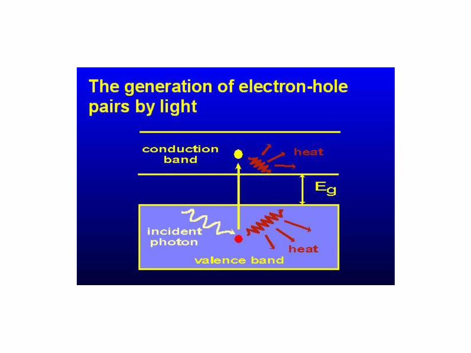
Silicon exhibits an energy gap of 1.14 eV.
Incoming photons with energy greater than this can excite valence
electrons into the conduction band thus creating electron-hole pairs. These
pairs diffuse through the silicon lattice structure. The average lifetime for
these carriers is 100 micro-sec. After this time the e-h pair will recombine.
Photons with energy of 1.1 to 5 eV generate single e-h pairs. Photons with
energy > 5 eV produce multiple pairs. Example: a 10 eV photon (Lyman
alpha) will produce 3 e-h pairs, on average, for every incident photon.
Soft X-ray photons can generate thousands of signal electrons make it
possible for a CCD to detect single photons. Limits in Silicon
Detectors: Photons with energy less than 1.1 eV (about 1.2 microns) pass
through silicon unimpeded. Photons with energy greater than 10 kev have
such small wave length that the probability of interaction is very small. To
use as an infrared imager, CCDs must be made of other material like
germanium (band gap 0.55 eV).
Photo-electric effect in silicon, X-ray detection