Embed Size (px)
Citation preview

GLOBAL WATCH MISSION REPORT
Electronics and electronicmaterials for harshenvironments – a mission to the USA
OCTOBER 2003

The DTI drives our ambition of‘prosperity for all’ by working tocreate the best environment forbusiness success in the UK. We help people and companiesbecome more productive bypromoting enterprise, innovation and creativity.
We champion UK business at homeand abroad. We invest heavily inworld-class science and technology.We protect the rights of workingpeople and consumers. And we stand up for fair and open markets in the UK, Europe and the world.
Global Watch MissionsThe UK Government Department of Trade and Industry(DTI) Global Watch service provides funds to assistsmall groups of technical experts from UK companiesand academia to visit other countries for short, factfinding missions.
Global Watch missions serve a number of relatedpurposes. These include establishing contacts withoverseas organisations for the purposes ofcollaboration, benchmarking the current status of UKindustry against developments overseas, identifyingkey developments in a particular field, new areas ofprogress or potentially disruptive technologies, orstudying how a specific industry has organised itselffor efficient operation or how governments, plannersor decision makers have supported or promoted aparticular area of industry or technology within theirown country.
DisclaimerThis report represents the findings of a technologymission organised by Faraday Advance (the FaradayPartnership in Automotive and Aerospace Materials)and EPPIC Faraday (the Faraday Partnership inElectronics & Photonics Packaging and InterConnect)with the support of the UK Department of Trade andIndustry (DTI).
The views and judgments expressed in this report arethose of the various authors and do not necessarilyreflect those of the DTI. This document records viewsand opinions attributed to organisations that werevisited in the course of the mission and are those ofthe personnel interviewed. Unless explicitly stated tothe contrary, they should not be taken as those of thecompany as a whole, its board or management.
Whilst every effort has been made to ensure that theinformation provided in this report is accurate and upto date, the DTI accepts no responsibility whatsoeverin relation to this information. The DTI shall not beliable for any loss of profits or contracts or any direct,indirect, special or consequential loss or damageswhether in contract, tort or otherwise, arising out of orin connection with your use of this information. Thisdisclaimer shall apply to the maximum extentpermissible by law.

Electronics and electronic materials for
harsh environments – a mission to the USA
OCTOBER 2003
1

TABLE OF CONTENTS
Preface 4
Acknowledgments 4
Executive summary 5
1 Introduction 7
2 Markets 92.1 Introduction 92.2 Well logging 92.3 Automotive 102.4 Aerospace 112.5 Military & defence 112.6 Power distribution 12
3 Semiconductor and relatedtechnologies 13
3.1 Introduction 133.2 Silicon carbide (SiC) 143.2.1 SiC growth 143.2.2 SiC devices 163.2.2.1 High power/voltage 163.2.2.2 High temperature 173.2.2.3 Microwave 173.3 III Nitrides 183.3.1 III Nitride growth 183.3.2 GaN devices 193.4 Microsystems and sensors 203.4.1 Introduction 203.4.2 SiC MEMS 213.5 Silicon on insulator (SOI) 223.6 References 25
4 Packaging and interconnecttechnology 26
4.1 Introduction 264.2 High temperature 264.2.1 Packaging 264.2.2 Die back-side metallisation 264.2.3 Solders for die attach 274.2.4 Silver for die attach 274.2.5 Contact metallisation 27
4.2.6 Passive components 284.2.7 Sensors 284.2.8 Uprating 284.3 Low temperature 284.4 High power and power density 284.5 High frequency 304.6 Heat extraction 304.7 Very high acceleration or shock 314.8 Medical/biosensors 31
5 Reliability 325.1 Introduction 325.2 Modelling reliability 325.3 Packaging for reliability at high
temperature: aerospace 325.4 Packaging for reliability at high
temperature: automotive 335.5 Packaging for reliability in the oil
industry 335.6 Reliability in advanced electrical
power systems 335.7 Reliability in die attach 335.8 Uprating 335.9 Storage in harsh environments 345.10 Reliability of components under
high G loading 345.11 Virtual qualification (VQ)
methodology 345.12 Remaining life assessment in
aerospace applications 345.13 Life consumption monitoring
(LCM) 355.14 Health and usage monitoring
systems (HUMS) 355.15 In-situ semiconductor health
monitors 355.16 Low temperature studies 355.17 Failure analysis 355.18 Advanced electrical
characterisation 365.19 Standards 365.20 Testing and reliability in
manufacture 36
2
ELECTRONICS AND ELECTRONIC MATERIALS FOR HARSH ENVIRONMENTS

3
ELECTRONICS AND ELECTRONIC MATERIALS FOR HARSH ENVIRONMENTS
5.21 Interface effects 365.22 Reliability in other devices:
detonators 375.23 Liquid crystal polymers (LCPs) 37
6 Emerging applications 386.1 Introduction 386.2 Benefits of SiC electronics to
automobiles and transportation 386.2.1 High temperature sensors and
control electronics 386.2.2 Interference immunity of radio
based avionics 396.2.3 High power electronics for
electric vehicles 406.3 Benefits of SiC electric power
systems 416.3.1 Energy savings in public power
distribution 416.4 Benefits of SiC electronics to
commercial and planetaryspacecraft 41
6.4.1 Increased satellite functionality at lower launch cost 41
6.4.2 Solar system exploration 426.4.3 Advanced launch vehicle sensor
& control electronics 426.5 Benefits of SiC electronics to
communications and radar 426.5.1 High power, high temperature
microwave RF electronic devices 426.6 Air Force perspective of SiC 43
7 R&D funding 447.1 Introduction 447.2 NASA Glenn 447.3 Joint industrial partnership (JIP) 447.4 Benefits to industry 457.5 Methodology to achieve
objectives 45
8 Conclusions andrecommendations 47
Appendix A: Mission participants 49
Appendix B: Host organisations 57
Appendix C: List of abbreviations 62
Appendix D: List of tables and figures 64

PREFACE
‘Harsh environments’ means different thingsto different people. This report concentratesmainly on wide bandgap (WBG)semiconductors and high temperatureapplications although other areas such as highpower/voltage applications are also covered.No silicon-on-insulator (SOI) manufacturerwas visited during the mission but themission members have extensive knowledgeof SOI so this area is also covered, as ismicrosystems.
It is clear that high temperature electronics(HTE) is emerging as a strategic technologyfor many countries, particularly those withhighly developed oil & gas and aerospacesectors. However, problems remain,particularly in establishing a reliable andsecure commercial source of componenttechnology. Even with reliable devices theproblems of packaging and system testingremain to be fully solved.
It is also clear that the UK could take aleading position in filling these gaps,particularly if with European assistance anindigenous supply of high temperaturesemiconductor components could beestablished, combined with integration of theexisting packaging and reliability testingexpertise available within the UK and Europe.
This report summarises the learning from themission and considers the implications for theUK. The chapters that follow have beenproduced by individual members of the group(sometimes in collaboration) in line with theirspecific areas of expertise.
Dr Colin JohnstonMission LeaderJanuary 2004
ACKNOWLEDGMENTS
Many organisations and individualscontributed to the success of this GlobalWatch Mission to the USA. The MissionOrganisers and participants would like toextend their particular thanks to:
The Department of Trade and Industry (DTI)Global Watch service.
The British Embassy in Washington DC andthe British Consulate-General in Atlanta.
The US companies, federal agencies andtrade & commerce organisations that hostedand met with the mission team. Thequestions asked of the mission hosts oftenskated close to proprietary information yetwere always answered in a helpful, honestand, as far as commercial confidentialitywould allow, full and open manner.
Thanks are also due to Pera Innovation Ltd fortheir help in the production of this report.
4
ELECTRONICS AND ELECTRONIC MATERIALS FOR HARSH ENVIRONMENTS

EXECUTIVE SUMMARY
Electronics for harsh environments arebecoming increasingly strategically important.Significant social and economic benefits canbe realised by placing electronics andelectronic systems in harsh environments.Applications include:
• Placing electronics closer to the ultimatepoint of use – often in high temperatureenvironments – to reduce weight,decrease connection complexity andimprove reliability.
• High power density electronics.• Placing electronics in chemically corrosive
or erosive environments to improvesensing capabilities and/or improve control– eg in chemical process plant or in marineenvironments.
• Using electronics at extremely low(cryogenic) temperatures – eg insuperconducting systems or spaceenvironments.
• Using electronics in high radiation fields inspace or for sensing and control functionsin nuclear systems.
The United States (US) is perceived to bethe world leader in the development andapplication of electronics for harshenvironments. A team of UK organisationswas brought together by Faraday Advanceand the EPPIC Faraday Partnership toundertake, under the sponsorship of theDepartment of Trade and Industry (DTI), aDTI Global Watch Mission to the US togauge current and future trends inelectronics and electronic materials for usein harsh environments. The mission tookplace during 20-24 October 2003 whendiscussions were held with the followingorganisations in the US:
• Technologies & Devices International (TDI) Inc.
• Computer Aided Life Cycle Engineering(CALCE) Research Center at the Universityof Maryland.
• Naval Research Laboratory (NRL).• Army Research Laboratory (ARL).• NASA Glenn Research Center.• Case Western Reserve University (CWRU).• Glennan Microsystems Inc (GMI).• Ford Motor Company.• GE Global Research.• Cree Inc.• Nitronex Corp.• Auburn University, including the Center for
Advanced Vehicle Electronics (CAVE).
This report details the main findings of themission and draws the conclusions that:
• There are strong interests in both the UKand the US to exploit electronics in harshenvironments. In fact there is a criticalneed in UK companies for reliableelectronics for operation at elevatedtemperatures and/or high powers.
• The level of investment for thedevelopment of electronics for harshenvironments in the US far outstrips thatavailable to the UK alone or evenEuropean-wide investment. The mainhistorical driver in the US has been itsinternal defence requirements, althoughsignificant investment is now beingdiverted from the energy sector.
• A wealth of different mechanisms havebeen exploited to fund start-up companiesin the field of wide bandgap (WBG)semiconductors in the US. However,these companies have all benefited from
5
ELECTRONICS AND ELECTRONIC MATERIALS FOR HARSH ENVIRONMENTS

6
ELECTRONICS AND ELECTRONIC MATERIALS FOR HARSH ENVIRONMENTS
extensive government research contractsplaced mainly through Department ofDefense (DOD) agencies.
• The commercialisation of WBGsemiconductor materials – silicon carbide(SiC) and gallium nitride (GaN) – is faradvanced in the US. Cree is theacknowledged world leader in the supplyof SiC substrates.
• The UK has no commercially activecompanies in silicon-on-insulator (SOI), SiCor GaN.
• The UK has research activities in GaN andSiC but these generally fall short of USdevice work although in some areas offundamental research the UK iscompetitive with the US.
• Europe (eg Siemens) is competitive withthe US in SiC high power/voltagetechnology.
• In microwave technology (both SiC andGaN) the US is far in advance of the UKand is protecting this position via exportcontrols (International Traffic in ArmsRegulations – ITAR).
• Europe (eg Osram) is competitive with theUS in some optoelectronic devices.
• Neither the US nor the UK has significantprogrammes in packaging for harshenvironments or in studying longer termreliability of systems and devices for harshenvironments.
• There is strong bilateral desire tocollaborate in developing technologies forharsh environments.
The principal recommendation of the missionteam is that the UK should focus on devicedevelopment and packaging and reliability forharsh environments.
If the UK or European Union (EU) couldprogress their SOI and/or SiC and/or GaNdevice manufacture in order to create devicefabs dedicated to the harsh and high reliabilitymarketplace then this would capture thebusiness and guarantee a reliable indigenoussource for the UK in this strategic niche market.

7
ELECTRONICS AND ELECTRONIC MATERIALS FOR HARSH ENVIRONMENTS
1 INTRODUCTION
Harsh environment products arecharacterised by extremes of ambientenvironment, power or power density, currentand operating frequency. Applications rangefrom down-hole (oil wells) to space and frompower generation and distribution toautomotive, aerospace and defence.
Another common requirement is longevity, toavoid interrupted service (infrastructure,transport, communications, mission success),because of inaccessibility forrepair/replacement (down-hole, space) or forlong term storage (defence). Add the need forsafety and the requirement for well-characterised reliable performance is clear.
The impetus behind exposing electronics toharsh environments is to improve systemarchitectures, in turn boosting safety,performance and efficiency – while lesseningenvironmental impact and deliveringoperational cost savings.
Significant benefits can be derived fromplacing electronics and electronic systems inharsh environments. For example, placingelectronics closer to the ultimate point of usein high temperature environments can reduceweight, simplify connections and improvereliability. Advantages are also achievable withhigh power density electronics, usingelectronics in chemically corrosive or erosiveenvironments, at extremely lowtemperatures, in high radiation and very highmagnetic fields.
The United States (US) is perceived to be atthe forefront of development and applicationof electronics for harsh environments, drivenby the needs of its defence and spacesectors.
Against this background, a UK Department ofTrade and Industry (DTI)-funded Global WatchMission to the eastern seaboard of the USwas undertaken in October 2003, to gaugecurrent and future US technology forelectronics and electronic materials for use inharsh environments, and benchmark the UK’scompetitive position in this field.
The mission was co-ordinated by two FaradayPartnerships – Faraday Advance (the FaradayPartnership in Automotive and AerospaceMaterials, represented by Oxford University)and EPPIC Faraday (the Faraday Partnership inElectronics & Photonics Packaging andInterConnect, represented by SheffieldUniversity). The mission participantcompanies were Alstom, BAE Systems,Goodrich, QinetiQ and QuantX.
The US host organisations represented world-leading research and development (R&D)establishments, manufacturers and end usersof electronics in harsh environments,including Cree Inc, the world leader inproduction of silicon carbide (SiC) and SiCdevices for harsh environments; the Centerfor Advanced Vehicle Electronics (CAVE) atAuburn University; Glennan Microsystems Inc(GMI), where representatives of Ford MotorCo and GE Corporate Research were present;the Computer Aided Life Cycle Engineering(CALCE) Electronic Products & SystemsCenter (EPSC) at the University of Maryland;Nitronex Corp; Technologies & DevicesInternational (TDI) Inc; the Naval ResearchLaboratory (NRL); the Army ResearchLaboratory (ARL); and NASA Glenn ResearchCenter.
The high level aim of the mission was one offact finding and technology transfer. Theapproach was to benchmark the UK against
8
ELECTRONICS AND ELECTRONIC MATERIALS FOR HARSH ENVIRONMENTS
North America – the perceived global leaderin the development and application ofelectronics for harsh environments – in anattempt to answer the following:
1 What companies are involved?
2 How are harsh environment materials andtechnologies being applied? That is,ascertain technical and market informationon electronics for harsh environments inNorth America.
3 What new applications and technologiesare in the pipeline? That is, determinetrends and drivers for developments inelectronics for harsh environments.
4 Where do the major opportunities lie? Thatis, raise awareness of UK technology forharsh environments to prospective NorthAmerican users and form transatlanticbusiness/academic links.
The specific objectives of the mission wereto:
• Assess collaboration/alliance opportunities;• Identify new materials, technologies and
products for UK companies;• Determine market perception and trends;• Determine how to exploit emerging harsh
environment materials and technologies;• Identify opportunities for UK developed
materials, technologies and solutions;• Identify possible secondment
opportunities; and• Understand how harsh environments are
perceived outside the UK.
The mission concentrated on wide bandgap(WBG) semiconductors and their associatedtechnologies and application drivenrequirements for high temperatureelectronics, high voltage/current electronicsand high frequency/power systems.

9
ELECTRONICS AND ELECTRONIC MATERIALS FOR HARSH ENVIRONMENTS
2 MARKETS
2.1 Introduction
‘Harsh environments’ means different thingsto different people. For example, it couldmean:
• High ambient temperature• Low (cryogenic) temperature• High voltage/current• Radiation fields• High frequency operation• High shock/impact• High vibration• Corrosive/erosive contact• Biological fluids
With the limited resources and time availablefor the mission it was possible to sample only a small selection of the available applicationareas. Since the technology focus was onWBG semiconductors, the definition of‘harsh’ was focused on three key topics:
• High temperature• High voltage/current – high electrical power• High frequency at high power
This focus limited the application areas whichwere addressed by the mission to:
• Well logging (oil & gas and geothermal)• Automotive• Aerospace• Military & defence• Power distribution
2.2 Well logging
Well logging and related borehole applicationsconstitute the most developed and appliedindustry which currently uses hightemperature electronics (HTE).
Well logging has been the main driving forceand leading financial sponsor for thedevelopment of HTE over the past 20 years.However, the use of HTE electroniccomponents within the petroleum explorationindustry is comparatively low volume and itsrequirements are highly specialised:
• HTE applications in petroleum explorationare not safety critical, in contrast to therequirements of many other industries, inparticular automotive and aerospace.
• Well logging equipment operates in arelatively stable thermal environmentcompared to the wide thermal cyclingexperienced in other applications. Failuresresulting from thermal cycling are as much
Well logging Automotive Aerospace Military & Power
defence distribution
High temperature Down hole Under hood More electric More electricPermanent Brakes
High voltage/current More electric More electric More electric Fixed– high electrical power Electronic distribution
starters Power generationMobile power
High frequency at high power Radar RadarElectronic warfare
Table 1 Applications for harsh environment electronics

10
ELECTRONICS AND ELECTRONIC MATERIALS FOR HARSH ENVIRONMENTS
a problem – if not more so – than failuresdue to sustained high temperatureoperation.
• Cost of the electronic components, whilstcertainly an important consideration, is notas critical within the well logging industryas it is for most other industry sectors.
There is a growing, significant and US nationalneed to unlock the natural gas resources thatexist at depths below 20,000 ft. In this harshenvironment, there are no known electronicshardware systems or modules that cansurvive these temperatures. This has requireddrillers to explore blind withoutinstrumentation below 20,000 ft. Withoutinstrumentation, drilling is very costly, slow,and often misses the target. To address thisthe US has initiated a joint industryprogramme led by Honeywell to develop acommercial source of silicon-on-insulator(SOI) devices.
2.3 Automotive
The automotive electronics sector representsthe largest potential market opportunity forHTE components, but also presents itstoughest challenge. HTE components standto make significant contributions to improvedsystem design, fuel efficiency and overallhigher performance. However, automotiveapplications continue to be characterised bythe most stringent pricing pressure of anysector covered in this report. In addition, therequirements for long-term reliability – overthe life of the vehicle – are very demanding.
Nevertheless, because the total availablemarket represented by automotive electronicsis so big, even a small-scale penetrationequates to a large market opportunity. Beforethis is achieved, however, much development isrequired not only for device technology but alsofor the mass production processes needed toachieve competitively priced components.
Due to the strict low-cost requirements in theautomotive industry, only silicon basedsolutions seem to be promising for mass
production targeting this high-volume cost-sensitive market. WBG semiconductors donot represent an affordable solution for theshort to medium term, althoughdevelopments in more electric technologymay well utilise SiC power devices.
A recent study by the Freedonia groupestimates that automotive electronics alonewill increase from $1,208 per vehicle in 1999to $1,864 per vehicle in 2009. While some ofthis increase will be due to the evolution oftelematic systems, most will be due to hybrid-vehicle electronics, collision avoidance andprotection systems, electronic steering andvehicle stability, and powertrain managementwith the incorporation of new systems suchas drive-by-wire control systems (throttle,steer, brake, shift and suspension by wire),collision avoidance systems (automaticbraking, steering and throttling with radar), andadvanced energy systems (42 V, fuel cellcontrollers and advanced energy converters).This accelerating trend towards moreadvanced electronics will increase the use ofvehicle electronics systems to anunprecedented level.
The unprecedented technological growth inautomotive electronics is best illustrated bythe evolution of one particular subsystem –powertrain management. Engine andtransmission management controllers nowsupport increased feature content, withadditional ‘smart’ subsystems added toprovide detailed and fast electromechanicalinterfaces. Modules such as voltageregulators, airflow meters, power switchingand smart solenoid switching systems helpthe electronic control systems to monitorpowertrain performance and adjustmechanical operations.
Future vehicle electronic modules will bephysically integrated with the mechanicalsystems they are intended to control. This willeliminate many of the module separationopportunities, and will place the electronicsdirectly in the thermal generation areas of the

11
ELECTRONICS AND ELECTRONIC MATERIALS FOR HARSH ENVIRONMENTS
mechanical systems and subject them toincreased temperatures.
The next generation of automotive electroniccontrol units (ECUs) is expected to bemounted close or directly onto the actuator –this means, for example, directly at the engine,in the transmission or near the brake disc. Thislocalisation of ECUs represents an evolutionarystep from the distributed mechanical systemtowards a functional integration of mechanicsand electrics with electronics.
2.4 Aerospace
For the aerospace industry, HTE technologycan potentially deliver enhanced functionalityin a range of applications, enabling denserelectronic systems with reduced load onaircraft systems and reduced weight.
In an application sector where safety issuesand regulations make component cost asecondary consideration, HTE technologycould achieve significant market penetrationin the next ten years. However, at present theuse of HTE components is still limited to lowvolume applications. The avionics sectortherefore promises to be an attractivestrategic niche market for HTE components.
The trend is for increased use of electronicsystems, ‘avionics’, as a proportion of thetotal functional content of aircraft and relatedaerospace systems. Furthermore, avionicssystems are required to carry out morefunctions in increasingly confined physicalspaces. This leads to denser circuits, whichpresent more demanding thermalmanagement requirements. Additionalrequirements, such as higher sustainedspeeds and longer flight durations, serve toamplify these problems.
Current aerospace technology involves theuse of individually optimised electrical,hydraulic and pneumatic systems to fulfil allthe requirements for operation. However, thecontinuing demands for greater fuel efficiencyand reduced running costs are unlikely to be
met by the incremental improvementsdelivered by the current approach todevelopment. The aim of the More ElectricAircraft (MEA) and More Electric Engine(MEE) concepts currently being developed byairframe (Boeing, Airbus) and aero engine(Rolls-Royce, General Electric, Pratt &Whitney) manufacturers is to replace theseindividual systems with one globally optimisedelectrical system with the key objectives of:
• Removal of low utilisation systems (egthree main hydraulic systems, ram-airturbine, gearboxes, drive shafts,mechanical pumps and hoses, airstarter);
• Integration of systems;• 10% reduction in weight;• Improved energy efficiency; and• Reduced purchase and, especially, running
cost.
Significant improvements in currenttechnology are required for the More Electricconcept to be realised, including improvedpermanent magnets and higher temperaturecapability electrical windings, lightweightconductors and improved power electronicsincluding capacitors and switching devices, aswell as control electronics operating atelevated temperatures.
The aerospace sector will utilise severalsemiconductor technologies and relatedpackaging, including SOI and SiC.
2.5 Military & defence
Electronic warfare – demands highperformance in ever-smaller packages, egpod-mounting vs internal modules. There isalso increased reliance on computer-basedsystems rather than human operators,making it likely that microelectronics will haveto function in smaller spaces with higherthermal loads.
Phased array radar – set to replace single-scanner based radar, PAR will require adrastic change in design approach to thethermal management task.

12
ELECTRONICS AND ELECTRONIC MATERIALS FOR HARSH ENVIRONMENTS
More electric – development of more electricplatforms in air, sea and land vehicles willmirror those for civil applications in theaerospace and automotive sectors. There willbe requirements for HTE and power devicetechnologies for power conditioning andelectrical actuation.
2.6 Power distribution
Power electronics has today only beenwidely applied in the field of electricaltransmission and distribution (T&D) in highvoltage direct current (HVDC) applications.These systems are based on thyristors andlarge banks of capacitors and high voltagetransformers, eg up to 400 kV with a typicaltransmitted power of hundreds ofmegawatts. Well suited to transmitting powerover long distances and under water, eg thelink between the UK and France, thesesystems can replace or reduce the need tobuild power stations using conventionalcarbon based fuels, eg oil, gas and coal,close to centres of large populations.
In the future, flexible alternating currenttransmission systems (FACTS) are expectedto become important to optimise the use ofexisting installations by increasing the powerflow capability, which is largely limited forstability reasons, and by improving the powerflow sharing. The wider adoption of FACTS isdependent on the availability of new powerswitching components which are expected tobe based on SiC. These components will offergreatly improved technical performance incomparison with the silicon basedcomponents available today.
Electrical supply networks are being driventowards the adoption of FACTS devices as theybecome comparatively weaker and weaker,compared with demand in particular for largescale networks. There are three key factors:
1 Total installed power generation arisingfrom the global demand is increasing at afaster rate than the availability of powertransmission.
2 Becoming significant and critical in themedium term, is the amount of poweroriginating from renewable sources – whichhave two inconvenient features: (a) they areunpredictable, eg power generation fromwind, where the level of energy generatedis directly dependent on the wind speed,and on occasions the wind stops forseveral days; and (b) the spread of manythousands of marginal low power sourcesthat may act independently of one anotheris a problem because without controlequipment the result will be a network withuncontrolled power flow and instabilitiesthat can easily lead to a blackout.
3 Environmental considerations lead to alimit on new overhead lines, or even theelimination of existing ones.
SiC based power electronic equipmentcombined with energy storage and real timeweb based control systems is expected toappear within seven years and revolutionise thisfield. Devices based on SiC offer an improvedperformance in the order of 100 to 1,000 timesin comparison with silicon and will ultimatelyenable the wide adoption of distributed energyand renewable energy sources.
A range of such devices will appear, eg: 10 kVinsulated gate bipolar transistors (IGBTs) withratings in the range 50 to 2,000 A; 1.7 kVmetal oxide semiconductor field effecttransistors (MOSFETs) with ratings of 10 to1,000 A; and companion high power diodes.These devices are expected to operate atjunction temperatures up to 200ºC. Theirapplication in power equipment will posemany difficult problems in terms of the highlevel of power switching which will occur. Thiswill very severely stress associatedcomponents, and pose many challenges insolving problems of stray inductance andcapacitance to earth.
Cree Inc are the leading producer of SiCsubstrates today and have ambitions to becomea world leading SiC device manufacturer.

13
ELECTRONICS AND ELECTRONIC MATERIALS FOR HARSH ENVIRONMENTS
3 SEMICONDUCTOR AND RELATED
TECHNOLOGIES
3.1 Introduction
As far as semiconductor materials areconcerned, the mission concentrated mainlyon WBG materials, although it is difficult toaddress electronics for harsh environmentswithout SOI, which has proven itself to be arobust, radiation-hard semiconductor and isnow finding application at moderate to hightemperatures.
WBG semiconductor materials havefundamental properties which make themhighly suitable for high power/voltage andextreme environment applications. This wasrecognised very early, but it was only withthe commercial availability of single crystalSiC from Cree Inc in North Carolina in theearly 1990s that extensive R&D was initiated.The US government has strongly supportedCree since then, and it is largely due to thatcontinuing support that WBG electronicdevices stand on the threshold of widespreaduptake today.
An excellent set of reviews of WBGtechnologies and their applications form theJune 2002 issue of Proceedings of theInstitute of Electrical and Electronics Engineers(IEEE) (see reference [1] in section 3.6).
The key properties of the dominant WBG
materials – the 4H polytype of SiC and galliumnitride (GaN) – are summarised in Table 2 andcompared with silicon (Si) and galliumarsenide (GaAs). Perhaps most significantly,WBG materials exhibit an electricalbreakdown field nearly an order of magnitudehigher than that of Si and GaAs. This can beexploited in many ways, but it immediatelytranslates to a higher operating voltage orlower resistance for electronic devices.
The wide bandgap means that the thermalgeneration of minority carriers is insignificantat temperatures below 1,000°C. Minoritycarrier generation results in parallel leakage indevices and hence inefficient operation. Bycomparison, minority carrier generation limitsthe operational temperature range of bulksilicon devices to below 200°C (SOI devicescan function to 300°C). In practice, themaximum operating temperature of WBGelectronic devices is limited by thetemperature stability of metallisation,dielectric layers and packaging, and not byany fundamental properties of the material.
Conversely, the wide bandgap results indopants which are relatively deep in energycompared to Si, limiting operation at lowtemperature for some device types. Inparticular, it is difficult to obtain high carrier
Property Si GaAs 4H-SiC GaN AlN
Bandgap (eV) 1.12 1.43 3.26 3.4 6.1
Breakdown field (V/µm) 30 30 250 250 1,200
Thermal conductivity (W/cm K) 1.5 0.5 4.5 1.5 3.3
Saturated velocity (cm/s) 1E7 1E7 2E7 1.5-2.7E7 1.8E7
Electron mobility (cm2/V s)@2E17 cm-3 600 4,000 400 1,000-2,000*
Hole mobility (cm2/V s) 150 30
Table 2 Electrical properties of relevant semiconductors (* in an HFET device)

14
ELECTRONICS AND ELECTRONIC MATERIALS FOR HARSH ENVIRONMENTS
concentrations and good ohmic contacts to p-type materials even at room temperature. It isnot yet clear whether this will prove a seriouslimitation for operation <0°C.
The power handling of large devices isdramatically affected by the ability of thematerial to control the temperature riseresulting from Joule heating. In this context,the high thermal conductivity of SiC (threetimes that of Si) is a tremendous advantage.GaN is not normally available as a freestanding material, and so is grown on differentsubstrates. When grown on SiC, GaN has alarge advantage over GaAs in thermalspreading in microwave applications, hencehas a high power handling capability.
The basic speed of transistors is set by thecarrier mobility and, in the case of highfrequency devices, the saturated velocity.Although lower than that of Si, the electronmobility of SiC is sufficiently high for goodperformance to be possible. The low holemobility of WBG materials is a limitation forbipolar devices. As we will see, thecombination of good electron mobility andhigh saturated velocity gives good highfrequency performance for GaN and its alloys.
3.2 Silicon carbide (SiC)
3.2.1 SiC growthSiC was the first WBG material to be availablein sufficiently large wafer size and quality forcommercial device exploitation to be feasible.The primary current application for thematerial is as the growth substrate for theblue light emitting diodes (LEDs) made by
Cree and by Osram. GaN technology isprincipally driven by this blue and UVLED/laser market where applications includeblue LEDs, full colour outdoor displays, whitelighting and, in the future, CD/DVD laserdiodes (LDs). However, the main futureapplication for SiC is in high power, highvoltage power electronics once the materialquality has matured.
SiC supply (Table 3) is dominated by Cree Inc,who use a physical vapour transport (PVT)technique. This batch based sublimationgrowth technique uses temperatures above2,000°C to form crystals which are currentlyavailable in either the 4H or 6H polytype.Wafer size is currently 75 mm in production,in a wide variety of product lines (n type, ptype and semi-insulating), and with 100 mmwafers in development. PVT is used by mostgroups worldwide to grow bulk crystals, butis intrinsically an expensive and slow process.Okmetic in Sweden is the only exception,where they are commercialising a hot-wallchemical vapour deposition (CVD) technique,and are in pilot production of 50 mm wafers.
Single crystal SiC substrates have improveddramatically over the last decade, but stillsuffer from a wide range of extended andpoint defects. The micropipe defect has beenthe focus of most effort until recently. It is anopen core screw dislocation, which takes theform of an open tube typically a fewmicrometres in diameter, and which goesstraight through the wafer. If the micropipeintersects a device, then low voltagebreakdown occurs.
Supplier 6H 4H SI Epitaxy
Cree Inc (Raleigh NC) N & P N & P 4H Yes, <50 µm
Dow Corning (formerly Sterling Semiconductor) N N 6H –
Bandgap Technologies (Columbus SC) N & P – 6H –
Okmetic (Sweden) – N & P 4H Yes, <6 µm
SiCrystal (Germany) N N – –
Sixon (Japan) N N 6H –
Table 3 Commercial suppliers of SiC

15
ELECTRONICS AND ELECTRONIC MATERIALS FOR HARSH ENVIRONMENTS
Figure 1 shows how the micropipe density hasreduced rapidly with time for successivegenerations of wafer size. Each increase inwafer size results in an increase in micropipedensity, subsequently being forced down to<10/cm2. This density allows high yieldproduction of devices with an area of a fewsquare millimetres, giving a current handling ofa few amps. At 100 mm wafer diameter, thewafer size will finally be large enough to justifymanufacturing of large power diodes (hundredsof amps), so extra effort is likely to be devotedto reducing the density even further.
Micropipe density can also be reduced duringgrowth of homoepitaxial layers of SiC.Technologies & Devices International (TDI) Incof Maryland use a hydride vapour phaseepitaxy (HVPE) growth technique to 'fill' themicropipes present in the SiC substrate. Thishas allowed them to make 1 x 1 cm micropipefree diodes. Cree Inc report that they also seedissociation of micropipes during epitaxy.Bandgap Technologies of South Carolina alsohave a micropipe overgrowth technique whichthey claim allows them to eliminate the defect.It is clear that improved production engineeringand increased wafer size will allow this problemto become insignificant in the next few yearsallowing increased power device size.
Lendenmann of ABB discovered in 2000 thatSiC PN diodes operated in forward bias couldgrow stacking faults in the junction, resulting
in a progressive increase in series resistance[2]. This has been traced to the presence ofbasal plane dislocations (BPDs) in the crystal,and extensive work in Sweden and the UShas led to an understanding of this defect andthe degradation mechanism.
Currently the density of BPDs is unacceptablyhigh at around 104/cm2. We heard at Creehow great progress has been made in bothbulk SiC growth and in SiC epitaxy incontrolling the defect, with the demonstrationof a wafer of PN diodes, ~60% of which donot show this degradation mechanism.Although there is still widespread concernthat the defect will affect the uptake ofbipolar devices, again it is clear that solutionsare possible and it will result only in a delay.
The bulk growth of SiC is possible with eithern- or p-type doping, but realistic devicestructures require the growth of controlleddoped layers using CVD. Again Cree are theprimary commercial source of epitaxiallygrown material. Indeed, although manycompanies have in-house growth capability,all UK activity is dependent on the Creeepitaxy service.
Information will shortly be available on theultimate performance of dislocation freematerial. NASA Glenn Research Center havedeveloped an epitaxial growth techniquewhich makes small regions of 3C polytype
Figure 1 Trend in micropipe densityfor production wafers of increasingsize at Cree Inc (after Hobgood,ICSCRM 2003)

16
ELECTRONICS AND ELECTRONIC MATERIALS FOR HARSH ENVIRONMENTS
material on 4H or 6H material which areentirely dislocation free. They are now startingto fabricate devices in this material.
3.2.2 SiC devices3.2.2.1 High power/voltageMost power applications require a highvoltage stand-off switch and a parallel diodeto accommodate reactive loads. However, thematurity and availability of the SiC versions oftwo components is very different. PowerSchottky diodes are commercially availablebut it will be around two more years beforethe first switches are available. Currently nospecifically high temperature capablecomponents are available.
A good review of the technology may befound in [3], with more recent data inconference papers (eg [4]).
SiC Schottky diodes are commerciallyavailable from Infineon in Austria and fromCree in the US. Limited by yieldconsiderations to a maximum die size of ~3 x 3 mm, Cree now have diodes with up to20 A capability and reverse blocking voltageof 600 or 1,200 V. As SiC crystal qualityimproves, current handling is expected tosteadily increase.
The maximum voltage handling from aSchottky diode is about 3 kV, above which it isessential to change to a bipolar diode. Asnoted in section 3.2.1, the availability of highvoltage diodes has been delayed by stackingfault induced reliability problems.Nevertheless, Cree have used >100 µm thickepitaxial material to demonstrate blockingvoltages as high as 19 kV. It will clearly be afew more years before >3 kV diodes areavailable.
GE Global Research Center have beenfabricating power Schottky diode moduleswith current handling up to 100 A by wirebonding multiple devices in parallel.
The problem component is the switch. Themarket likes normally-off transistors and sofavours power devices such as MOSFETs orIGBTs. SiC can be oxidised and used to forma MOSFET that is directly analogous to Sidevices. However, the SiC/SiO2 interface isplagued by high interface state densities andpoor dielectric reliability at elevatedtemperature. This has meant thatperformance has barely exceeded thatachieved by Si based devices.
This situation has changed over the lastcouple of years with the discovery thatannealing in a nitrous oxide (N2O) ambientcan dramatically improve the stability andquality of the oxide interface, makingmetal-oxide-semiconductor (MOS) baseddevices much more feasible. At Cree weheard that they are developing a 1.7 kVMOSFET with a 1 to 2 A current handlingcapability. They would not say what theirplans are for this product but suggestedthat samples would be available in lessthan two years. Infineon are plainly at asimilar stage and reported >1,000 hour lifefrom similar performance devices at therecent International Conference on SiC andRelated Materials (ICSCRM) conference inLyon in October 2003.
Many other types of device have beendemonstrated including bipolar junctiontransistors (BJTs), IGBTs, gate turn-offs(GTOs) and junction field effect transistors(JFETs). The latter device, although normallyon, has been the focus of considerableinterest when coupled with a conventionalSi MOSFET to form a cascode. Thiscascode arrangement gives the normally-offadvantage of a MOSFET together with thefast high voltage/current handling of an SiCswitch. The great advantage of the SiCJFET device is that there are no highelectric fields across oxides (with theirconsequent reliability problems), making itmuch more reliable.
17
ELECTRONICS AND ELECTRONIC MATERIALS FOR HARSH ENVIRONMENTS
The only disadvantage for the Si/SiC cascodeis that high temperature operation is limitedby the Si component. Infineon in Europedemonstrated such a component severalyears ago and is investigating the market tosee whether there is sufficient demand tojustify launching a product. In the US, RutgersUniversity together with United SiC Inc havedeveloped vertical JFETs with highperformance (6 A, >1,000 V). GE are alsoinvestigating this same cascode approach.
3.2.2.2 High temperatureThere are many scenarios which require hightemperature electronics, and each tends torequire a separate device technologydevelopment. This is a major focus ofGlennan Microsystems Inc and relatedactivities in Ohio.
NASA Glenn Research Center (Dr PhilipNeudeck) believes that silicon will addresslow power applications up to 300°C, with SiC only being required above thattemperature [5].
The most extreme environment beingseriously addressed is 600°C capableelectronics for jet engine applications. NASAGlenn Research Center are developing an SiCactive electronic technology. At thistemperature, dielectric reliability issues meanthat the JFET is the device of choice. Theyhave demonstrated NAND and NOR gates at600°C, and are currently fabricating a JFETbased amplifier which uses a two level metalprocess, with a target of 1,000 hours life. Themain challenges lie in the areas of ohmiccontact stability, charge trapping and hightemperature packaging. A strong emphasis ison the integration of the electronics withmicro-electro-mechanical systems (MEMS)technology.
GE developed an SiC negative-channel metaloxide semiconductor (NMOS) integratedcircuit (IC) technology about 10 years ago,including a 300°C opamp. However, the oxide
reliability/stability was poor and the attemptwas abandoned. GE now feel that it is time torevisit SiC MOSFETs given the recentadvances in SiC/SiO2 interface quality. Theyare embarking on a smart-power activity,although primarily aimed at room temperatureapplications.
GE manufacture SiC photodiodes forapplication as flame sensors in their gasturbines. SiC photodiodes are stable underhigh UV irradiance and have low dark current.
3.2.2.3 MicrowaveDue to basic materials properties, SiC deviceswill not operate at as high a frequency as theemerging GaN devices. However, the materialquality is better, so reliable, high power, radiofrequency (RF) devices can now be produced.
Since the physical size of the active part of amicrowave transistor is tiny, micropipedefects are unimportant. More significant hasbeen the elimination of vanadium impuritiesfrom insulating SiC, and it is the recentavailability of vanadium free insulatingsubstrates that has made it possible tofabricate stable, reliable power transistors.
Cree Inc have now launched their secondgeneration SiC microwave metalsemiconductor field effect transistor(MESFET) process. The first product is a 10 Wpower device which operates up to 2.4 GHz(package limited), with a primary aim oftargeting the wireless base station business.The main benefit compared to conventional Silateral double-diffused MOSFET (LDMOS) isease of RF matching and wideband operation(they have made a 1 - 900 MHz, 10 dB gainwideband amplifier). The device is apparentlystable, showing essentially no degradation at175°C in 2,200 hours, and only limiteddegradation at a 240°C junction temperature.For harsh environments the device wouldprobably need repackaging, however Creestate that there are no plans to make theirdevices available in die form.

18
ELECTRONICS AND ELECTRONIC MATERIALS FOR HARSH ENVIRONMENTS
Cree have also established a full SiCmonolithic microwave integrated circuit(MMIC) process suitable for use up to about6 GHz. This process was established withthe help of a $26 million Department ofDefense (DOD) contract. An example of thecircuits which have been implemented is a30 W, 1.2 - 3.5 GHz, 8 dB gain amplifier with50 ohm input and output. InternationalTraffic in Arms Regulations (ITAR)restrictions have been applied to this MMICprocess; it is only available for use by UScompanies in the US.
Cree are the only group selling an SiCmicrowave device although other groups areactive in the field. Northrop-Grumman have avery impressive SiC static-induction transistorprocess which has been used in L- and S-band radar modules, but it is entirely forinternal use and they have no plans forcommercialisation. GE are undertakingresearch into SiC MESFETs and have madedevices with a width of up to 20 mm whichare stable for 1,000 hours at 225°C. Theirprimary interest is in the use of these devicesfor microwave excited solid-state lighting.Several Japanese groups are active, and inEurope Thales has an SiC MESFET process,and there are two active groups in Sweden.
3.3 III-Nitrides
3.3.1 III-Nitride growthAlthough GaN and its alloys are primarily usedfor LED and laser diode fabrication, there isintense interest in their use for microwaveapplications.
In the past it has not proved possible to growlarge crystals of either GaN or aluminiumnitride (AlN) so most research has beenfocused on heteroepitaxial growth ondissimilar substrates. However, there is nowsignificant progress being made in the growthof AlN and GaN crystals, particularly atUnipress in Poland, in Japan, and under DODfunding in the US.
TDI are using a CVD growth technique togrow both AlN and GaN crystals. They havebeen able to grow AlN crystals which can besliced into 25 mm diameter wafers. Thesehave demonstrated >108 ohm cm resistivityand 3.3 W/cm K thermal conductivity, makingit a very attractive substrate for microwaveapplications. They are willing to supply wafersto selected customers. GaN growth is lessmature but 1 cm crystals have been grown.Other groups working on GaN bulk growthinclude Emcore and GE.
Available from Sumitomo in Japan are GaNlayers formed by HVPE growth on sapphire,followed by removal of the substrate by lasertreatment. Overall, despite encouragingprogress, it is clear that it will be severalyears before bulk material is sufficientlymature to have a significant impact on thedevice market.
Since GaN is not widely available in singlecrystal boule form, GaN and its alloys havebeen grown epitaxially on dissimilarsubstrates, in particular sapphire and SiC.There is a large lattice mismatch of ~3% onSiC and ~12% on sapphire and a significantdifference in thermal expansion coefficient.A very high density of dislocations in thestructures is therefore required toaccommodate the mismatch (typically 108-1010 cm-2 of threading dislocationscompared to ~103 cm-2 on GaAs or <1 cm-2 on Si).
In general, improved electrical, andoutstanding thermal performance is seen onSiC compared to sapphire substrates.However, the cost for an insulating SiC wafer(before epitaxy) is currently ~$5,000/wafer(50 mm diameter), compared to <$100/waferfor 50 mm substrates. Hence despite its poorthermal conductivity, cost and manufacturingconsiderations have led to sapphire beingwidely used as a substrate material,particularly by the Japanese.
19
ELECTRONICS AND ELECTRONIC MATERIALS FOR HARSH ENVIRONMENTS
More recently, GaN growth has beendemonstrated on the (111) face of Sisubstrates. With Si substrates, wafer size andwafer cost ceases to be an issue. In the US,Nitronex Corporation of Raleigh (NorthCarolina) are the leading exponent of thisapproach. They span out of North CarolinaState University (NCSU) in 1999 and havenow received >$40 million in venture capitalto develop this technology for wireless basestation applications. They use a patentedprocess to grow 3 µm layers of crack-freeGaN on 100 mm Si wafers despite themismatch being even worse than forsapphire. A major benefit is that thecrystalline perfection of the Si substrate givessuperb uniformity in the heteroepitaxy. InEurope, Picogiga (now owned by SOITECHbased in Grenoble) have just announced theavailability of 100 mm GaN on Si substrates.
3.3.2 GaN devicesDOD-funded activity in GaN devices focuseson the AlGaN/GaN high electron mobilitytransistor (HEMT) fabricated on SiCsubstrates. The Defense Advanced ResearchProjects Agency (DARPA) is funding deviceactivity at Cree, Raytheon, HRL, Northrop-Grumman and the universities of Texas,Santa-Barbara and South Carolina. The USArmy, Navy (ONR) and Air Force are allfunding activities in this area. The emphasis ison high power over wide bandwidth, with asecondary emphasis on higher temperatureoperation.
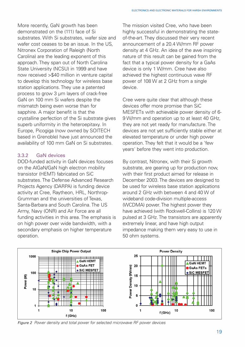
The mission visited Cree, who have beenhighly successful in demonstrating the state-of-the-art. They discussed their very recentannouncement of a 20.4 W/mm RF powerdensity at 4 GHz. An idea of the awe inspiringnature of this result can be gained from thefact that a typical power density for a GaAsdevice is only 1 W/mm. Cree have alsoachieved the highest continuous wave RFpower of 108 W at 2 GHz from a singledevice.
Cree were quite clear that although thesedevices offer more promise than SiCMESFETs with achievable power density of 6-9 W/mm and operation up to at least 40 GHz,they are not yet ready for manufacture. Thedevices are not yet sufficiently stable either atelevated temperature or under high poweroperation. They felt that it would be a 'fewyears' before they went into production.
By contrast, Nitronex, with their Si growthsubstrate, are gearing up for production now,with their first product aimed for release inDecember 2003. The devices are designed tobe used for wireless base station applicationsaround 2 GHz with between 4 and 40 W ofwideband code-division multiple-access(WCDMA) power. The highest power theyhave achieved (with Rockwell-Collins) is 120 Wpulsed at 3 GHz. The transistors are apparentlyextremely linear, and have high outputimpedance making them very easy to use in50 ohm systems.
Figure 2 Power density and total power for selected microwave RF power devices

20
ELECTRONICS AND ELECTRONIC MATERIALS FOR HARSH ENVIRONMENTS
In their current development phase, a majorbenefit is the low cost of the substratesallowing large scale testing to be carried out.Nitronex have processed 1,491 wafers in thelast year, something that would be prohibitivelyexpensive with SiC substrates. A reliability testis under way at 200°C, with apparently nosignificant degradation after 2,000 hours. Thecompany is entirely focused on the WCDMAmarket, so no effort has been expended onthe issues of using GaN HEMTs on Si athigher frequencies, where there has beenconcern about RF losses in the substrate.
3.4 Microsystems and sensors
3.4.1 IntroductionMicrosystems or micro-electro-mechanicalsystems (MEMS) are being developed tomerge sensing, actuating and computing inorder to realise new systems that bringenhanced levels of perception, control andperformance.
MEMS are usually realised on a common Sisubstrate through microfabricationtechnology. While the electronics arefabricated using IC process sequences (egCMOS, bipolar, or BICMOS processes), themicromechanical components are fabricatedusing compatible ‘micromachining’ processesthat selectively etch away parts of the Siwafer or add new structural layers to form themechanical and electromechanical devices.
MEMS promises to revolutionise nearly everyproduct category by bringing together Si basedmicroelectronics with micromachiningtechnology, making possible the realisation ofcomplete systems-on-a-chip. MEMS is anenabling technology allowing the development ofsmart products, augmenting the computationalability of microelectronics with the perceptionand control capabilities of microsensors andmicroactuators and expanding the space ofpossible designs and applications.
Microelectronic ICs can be thought of as the‘brains’ of a system; MEMS augments this
decision-making capability with ‘eyes’ and ‘arms’to allow microsystems to sense and control theenvironment. Sensors gather information fromthe environment through measuringmechanical, thermal, biological, chemical, opticaland magnetic phenomena. The electronics thenprocess the information derived from thesensors, and through some decision makingcapability direct the actuators to respond bymoving, positioning, regulating, pumping andfiltering, thereby controlling the environment forsome desired outcome or purpose.
Because MEMS devices are manufacturedusing batch fabrication techniques similar tothose used for ICs, unprecedented levels offunctionality, reliability and sophistication can beplaced on a small Si chip at a relatively low cost.
Although there are numerous possibleapplications for MEMS, the missionconcentrated on MEMS devices which couldbe utilised at high temperature, so most ofthe already well established Si technology willnot be reviewed here. Europe is well placedin conventional MEMS technology and leadsthe way in many areas, eg accelerometersfabricated using the Bosch process.
The key MEMS host during the mission wasOhio-based Glennan Microsystems Inc (GMI),founded in 1998 as a public-privatepartnership (Glennan Microsystems Initiative)with a five-year focus and $21 millioninvestment. Named for T Keith Glennan, thefirst administrator of NASA and a formerpresident of Case Western ReserveUniversity (CWRU), GMI focuses on physicalsensors, chemical sensors and actuators inharsh environments.
GMI leverages the R&D capabilities andapplication interests of partners such asNASA Glenn Research Center, CWRU, otheracademic institutions, industry andgovernment. These partnerships provide GMIwith resources well suited to expanding thedevelopment and use of microsystems in a

21
ELECTRONICS AND ELECTRONIC MATERIALS FOR HARSH ENVIRONMENTS
variety of ways. GMI's purpose is to assisttechnology companies by providing forresearch, development, andcommercialisation of microsystemstechnology through strategic alliances andbusiness acceleration.
3.4.2 SiC MEMSFLX Micro, formerly known as FiberLead,provides innovative microsystems technologysolutions based on its extensive expertise inmicromachining and automation. The companyoffers an advanced microsystems toolkit,including MEMS-based product development,state-of-the-art process technologies for SiC,low-cost MEMS prototyping, and uniqueautomation capabilities for high precisionpositioning. FLX Micro was a spin out fromGMI and a partner in MUSiCSM.
MUSiCSM, a multi-user MEMS prototypingservice, is the first and only surfacemicromachining process that utilises SiCstructural layers. SiC possesses excellentmechanical, chemical and thermal properties,which allow it to extend microsystemstechnology to a wide range of applicationsand operating environments. The MUSiCSM
process, which is offered exclusively by FLXMicro, provides low-cost access to MEMSprototyping using this superior material.
MUSiCSM combines multiple chip designsonto a single large-area substrate to takeadvantage of economy of scale. This way,each user purchases only a portion of thewafer’s real estate, allowing designs fromdifferent users to be fabricatedsimultaneously. The inaugural MUSiCSM run
Figure 3 MUSiCSM process flow

22
ELECTRONICS AND ELECTRONIC MATERIALS FOR HARSH ENVIRONMENTS
contained designs from 13 internationalcustomers across a variety of industries –ranging from automotive to biomedical and toconsumer products and communications.
MUSiCSM is an eight mask surface machiningprocess with polycrystalline SiC structurallayers. The process flow is shown in Figure 3.
The development of SiC MEMS could besignificant for the penetration of MEMSdevices into all harsh environments given thesuperior resistance shown by SiC over manyother MEMS substrate materials.
Other significant MEMS and sensortechnology reviewed by the mission includedan advanced oxygen pump sensor system forautomotive exhaust sensors being developedby Ford Research at Dearborn (Michigan) foractive engine combustion control throughexhaust gas monitoring of oxygen and NOx.
3.5 Silicon on insulator (SOI)
Although the mission did not visit anycompanies or organisations directly involvedin SOI technology, this area is of paramountimportance to electronics for harsh
environments, particularly for the two majortechnology segments of high temperatureand radiation hardness.
All harsh environment electronic systems aredependent upon the performance and life ofSi components, from a simple field effecttransistor (FET) to very large scale integratedcircuits (VLSIs). Conventional semiconductorcomponents are based on bulk Si structuresbut these devices suffer from performanceand life concerns at elevated temperature. Atleast three major challenges exist in the bulkSi CMOS structure at elevated temperature:
1 Device leakage current due to bipolartransistors found in bulk CMOS.
2 Gate oxide leakage and punch through.3 Surface metal migration and wire bond to
die metal inter-diffusion.
Leakage current due to bipolar transistors inthe bulk CMOS increases with temperature.The effect on the operation of a digital IC is to(a) reduce a logic high output, (b) increase alogic low output, and (c) reduce the thresholdvoltage for the next stage until eventually thedevice stops working. Similarly, in a digital
Figure 4 CMOS inverter circuit

N-well
component the delays increase, the slew ratereduces and the device once again will stopfunctioning at a (device) specific temperature.In an analogue component the leakagecurrent will affect almost all parameters suchas input bias and offset current, input offsetvoltage to gain bandwidth and noise margins.
The life of a CMOS component is also affectedby the increasing leakage current of the bipolartransistors. As the temperature is increasedthe leakage current in the bipolar transistorswill eventually turn on both PMOS & NMOStransistors (destructive latch up). This will alsohappen at a lower temperature in time as theleakage current in the bipolar transistorsincreases with time at elevated temperatureand will result in destructive latch up.
SOI (oxygen implantation) can solve the hightemperature leakage problem. CommercialSOI will not yield a harsh environment
product as the reason for developing bothpartially and fully depleted SOI is to shrinkfeature size. Copper metal systems are usedin commercial devices and Si contaminationwould be a concern at elevated temperature.SOI is a standard bulk Si process with addedoxygen implantation process that blocks offnumerous leakage paths. A comparison ofbulk Si vs SOI can be seen in Figure 5.
The effect of the buried oxide layer onleakage current paths is illustrated in Figure 6.
Another life issue with bulk Si at elevatedtemperature is gate oxide breakdown. Astemperature increases gate oxide breakdownoccurs, first seen as increased leakage thenas gate punch through. The effect of this canbe seen in loss of non-volatile memory due todestructive gate breakdown over time attemperature. The solution is a thicker gateoxide with special features.
23
ELECTRONICS AND ELECTRONIC MATERIALS FOR HARSH ENVIRONMENTS
Figure 5 Comparison of bulk Si vs SOI

There are further life concerns associatedwith bulk SI metal systems at hightemperature. Standard aluminium metal willmigrate at elevated temperature and this canresult in open or short circuit devices.Migration is a function of temperature andcurrent density. This is also a concern in dieshrink at lower temperatures as the currentdensity is generally increasing in the smallfeature size. This explains why new devicesare rarely specified for long life even at 105°C.Honeywell are the industry leaders in the fieldof high temperature SOI and offer aluminiummetal with a titanium tungsten barrier layer tomitigate the migration.
The life specification for a Honeywell SOIcomponent (commercially available) withaluminium metal and a titanium tungstenbarrier layer is:
• 45,000 hours at 225°C• 90,000 hours at 200°C• 130,000 hours at 180°C• Excursions to 300°C
Failure is defined as a 10% increase in diemetal resistance. Honeywell have developedand demonstrated tungsten gold metal thatwill increase the life at 300°C to 45,000 hoursbut this is not commercially available. It isthought that SOI for 300°C performanceshould be changed from the Honeywellpartially depleted to a fully depleted process.A lifetime comparison between bulk Si andHoneywell partially depleted SOI with variousmetal systems is presented in Figure 7.
The metal system is key to a robust deviceprocess for elevated temperature, and specialSOI device parameter adjustment will beessential. A list of the Honeywell devicedesign parameter adjustments made inaddition to their special die metal structures isshown in Table 4.
24
ELECTRONICS AND ELECTRONIC MATERIALS FOR HARSH ENVIRONMENTS
Figure 6 Effect of buried oxidelayer on leakage current paths

3.6 References
[1] J C Zolper and B V Shanabrook,'Special issue on wide bandgapsemiconductor devices', Proc IEEE,vol 90, 2002.
[2] H Lendenmann, F Dahlquist, NJohansson, R Soderholm, P ANilsson, J P Bergman and P Skytt,'Long term operation of 4.5 kV PiNand 2.5 kV JBS diodes', MaterialsScience Forum, vol 353-356, pp 727-730, 2001.
[3] A Elasser and T P Chow, 'Siliconcarbide benefits and advantages forpower electronic circuits andsystems', Proc IEEE, vol 90, pp 969-986, 2002.
[4] T P Chow, 'High-voltage SiC devicesfor power electronics applications -future prospects', in Proceedings of10th European Conference on PowerElectronics and Applications,Toulouse, 2-4 September 2003,2003.
[5] P G Neudeck, R S Okojie and L YChen, 'High temperature electronics- a role for wide bandgapsemiconductors?', Proc IEEE, vol 90,pp 1065-1076, 2002.
25
ELECTRONICS AND ELECTRONIC MATERIALS FOR HARSH ENVIRONMENTS
Issue Primary mitigation strategies
Junction leakage SOI process
Sub-threshold Vt adjustmentleakage
Electromigration Design rules to lower maximum current density
Reduced mobility Design adjustments:Temp. compensated biasingLarger digital devices or derate clock frequency
Bias voltage drift Design techniques (eg ZTC biasing)with temperature
Self-heating Design for lower power density, layout floorplanning, metal-interconnect heat-spreading etc
Floating body Partially-depleted SOI with body tieeffects Layout rules for max spacing to
body-tie contacts
Back-gate Increased back-oxide thicknesstransistors
Table 4 Mitigation strategies for issues in harshenvironment SOI (Honeywell)
Figure 7 Lifetime comparison between bulk Si andHoneywell partially depleted SOI with various metalsystems

26
ELECTRONICS AND ELECTRONIC MATERIALS FOR HARSH ENVIRONMENTS
4 PACKAGING AND
INTERCONNECT TECHNOLOGY
4.1 Introduction
Higher operating temperature capability insemiconductor devices offers a number ofadvantages. If they are allowed to operate athigher temperatures, the coolingarrangements can be smaller, lighter andlower cost. Alternatively they can providegreater reliability/longevity than conventionaldevices at the same temperature. Packagingand interconnect are key elements inachieving both performance and reliability.
Overall, the mission saw little mature packagingand, in view of its importance, relatively littleeffort on the development of packaging,interface materials or interconnectionto/between devices. Nevertheless, some of thehost organisations are clearly making good orexcellent progress in their selected areas ofpackaging/interconnect development. Mosteffort focused on high temperature applications.
Packaging and interconnect technologies foroperation above 300°C are not yet mature.There remain major challenges, including thechemical, physical and electrical stabilities andcompatibilities of materials and interfaces atsuch high temperatures. The very widetemperature range increases the stresses dueto coefficient of linear thermal expansion (CTE)differences between the materials. This mayaffect package/assembly integrity and even theperformance of the WBG semiconductordevices themselves. The very hightemperatures may also cause outgassing,hence contamination within hermetic packages.
The realisation of practical high temperatureelectronics will require innovative packagingmaterials and package concepts. For the fullpotential to be implemented, passivecomponents (resistors, inductors and
capacitors) capable of withstanding similartemperatures will also be needed.
4.2 High temperature
4.2.1 Packaging NASA Glenn Research Center is developingAlN packaging with commercial thick-film goldmetallisation, for 200°C applications.
Auburn University has developed techniquesto make virtually hermetic packages using aliquid crystal polymer (LCP). LCP has veryattractive properties: modest CTE (8 or 17 ppm/°C); very low water absorption(<0.04%wt); very good dimensional stability(<0.1%); and virtual impermeability tomoisture, oxygen, other gases and liquids. Itis also halogen-free and flame retardant. Itcan be readily used with standard processesfor fine-feature printed circuit board (PCB)fabrication, including laser cutting ofmicrovias, and for component assembly. Acavity lid and a base substrate of LCP aremetallised and joined by solder at 250°C,under vacuum. Packages have passed bothcoarse and fine leak testing. Laser welding ofthe LCP itself is also being developed.
The benefits of polymer packages over metalor ceramic packages are reductions in weightand cost, also size (unless the number ofconnections is small), and improved electricalperformance (lower parasitics), especially athigh frequencies/data rates.
4.2.2 Die back-side metallisationAlong with the package activities, AuburnUniversity’s Center for Advanced VehicleElectronics (CAVE) is developingmetallisations for the die back-side for hightemperature use, eg NiSi, Ti/Pt/Au,SiC/SiO2/Cr/NiCr/Au.

27
ELECTRONICS AND ELECTRONIC MATERIALS FOR HARSH ENVIRONMENTS
4.2.3 Solders for die attach After ageing/temperature cycling, high-tin andhigh-lead solders exhibit a large amount ofintermetallic growth, which weakens thehigh-tin solder (from Ni/Pd/Au plating finishfor high-tin solder, SnPb plating for high-lead).High-lead attach materials have poor fatigueproperties.
CAVE is developing processes for die attachof SiC devices able to withstandtemperatures up to 350°C, using Au80/Sn20.
4.2.4 Silver for die attachThis lead-free material is sintered, with thedie in place, in a chamber at high pressureand at 250°C, a temperature lower than themelting point of the attach material. Thisenables subsequent joining/processing attemperatures above 250°C, eg lead-freesolder reflow at 260°C. Die shear strengthsexceed those of traditional die attachmaterials.
4.2.5 Contact metallisationNASA Glenn Research Center has developeda high temperature ohmic contact, Ti/TaSi/Pt,on degenerate n-type SiC, which is still ohmicand reliable after hundreds of hours at 600°Cin air. The implication is that this type ofcontact could be used without the need for ahermetic package.
However, the availability of reliable ohmiccontacts to p-type materials is still achallenge. The contact metallisation willprobably have to be different, according toNASA Glenn, which is looking at some ‘non-conventional’ approaches.
Auburn University is developing ohmiccontacts for the electronic connection padsand for the wirebonding process. A multilayerdeposit is annealed to form a diffusion barrieragainst oxygen and mass exchange. Theohmic contact is Ni or NiCr for n-type SiC,and heavily doped p-type SiC, AlTi or NiAl formoderately doped p-type SiC.
Figure 8 Metallisation for power devices (Auburn University)
Cap layer for wire bonding or connectDiffusion barrier “XY” prevents massexchange and oxygen incorporationIntermetallic “YZ” forms low barrierlinear transport character
Prevention of oxygen incorporationcritical for stable, high temperatureperformance of both ohmic andrectifying contacts
Typical ohmic contactformation metallurgy
AS DEPOSITED POST ANNEAL

28
ELECTRONICS AND ELECTRONIC MATERIALS FOR HARSH ENVIRONMENTS
For Schottky contacts, Auburn University usessintered Ni for n-type SiC. Barriers againstdiffusion and oxidation are TaSi2(N), RuO andindium tin oxide (ITO). The final layer for thewirebond or other connection is Au/Pt.
Wirebonding trials have encompassed Pt andAu wire, 0.25 mm diameter, the Pt wirebondsbeing on the substrate only, the Au on bothdevice and substrate, the substrate pad beingNi/Cu with thick Au plating. This combinationhas given promising results, but work isunder way on pads of Cr/NiCr/Au.
4.2.6 Passive componentsSiC resistors which hold their value to betterthan 1% after 2,500 hours at 500°C havebeen demonstrated by Caldus SemiconductorInc. According to General Electric,potentiometers, resistors and capacitors areavailable (at least in the US) for operation upto 175°C, but a longer, more reliable life (>20years) is desired, eg for down-holeapplications.
4.2.7 SensorsHigh temperature sensing is required for engineexhausts (automotive, aircraft and rocket) at 400to 800°C. For such sensors, the packagingusually represents >50% of the overall cost. SiCMEMS capacitance sensors are beingdeveloped by CWRU for 400°C operation. Foroptical communications, GaAs sensors areavailable able to operate at >250°C. Anattractive substrate for high temperaturesensors is polycrystalline SiC, available fromCWRU, as it is very robust and stiff, so providingvery high Q, and does not suffer from ‘stiction’,which is often a problem in MEMS devices. It isstable up to 1,100°C, with no microstructuralchanges. CWRU is seeking to replace Si bypolycrystalline SiC for micromachined parts, butthe deposition temperature is 900°C, comparedto 600°C for Si.
4.2.8 UpratingMost devices are specified for operation in atemperature range of 0 to 70°C or -40 to
85°C, so for confident use outside thespecified range there is a need to ‘pre-screen’components and to identify the level of riskassociated with such ‘uprating’. To date, theuprating at CALCE has been limited to 205°C.
CALCE has developed upratingmethodologies and uprateability riskassessment criteria and methods forassigning the uprateability risk levels toindividual components, including a focuseddata collection and analysis process whichprovides a numerical risk level to eachcomponent, predicting the risk level involvedwith uprating it. A case study has beenperformed on a new, fully automated digitalengine controller (Honeywell) with 519 partsfrom 44 manufacturers (contact Dr DigantaDas: [email protected]).
The commonest fault mechanisms in‘commercial’ product plastic packaging arewater absorption, wirebond pad corrosion,and movement of the moulded plastic overthe die, causing damage to both devices andwirebonds.
CALCE has concluded that operation outsidethe temperature range of the data sheet ismore likely to affect performance than reliability.
4.3 Low temperature
CALCE is investigating techniques for lowtemperature, ie -120 to -150°C, for NASA.Topics include :
• Dominant package-related failuremechanisms for chip-on-board at lowtemperature.
• Behaviour of selected packaging materialsat -120°C.
• Stresses on interconnects and die and therelationship to observed failuremechanisms.
4.4 High power and power density
High power devices are made on either SiC,GaN or AlGaN wafers, with SiC beingfavoured for high temperature applications as

29
ELECTRONICS AND ELECTRONIC MATERIALS FOR HARSH ENVIRONMENTS
its thermal conductivity is three times that ofSi and GaN and nine times that of GaAs.
For high power devices, CAVE favours Si3N4
as a package/substrate material because ofits combination of key thermomechanicalproperties (see table 5 at end of this chapter).An adhesion layer of Ti is used, with a Cu-Agbraze and copper foil up to 1 mm thick. Thelatter can serve as overhanging connectiontabs. (See also section 4.6 ‘Heat extraction’.)
Key challenges are the avoidance ofdegradation of metallurgical bonding materialsover extended time at high temperature, andinsulator material for high temperatureoperation with air or gas in the cavity of thepackage. For high voltage insulation, a coatingis applied after wirebonding, but at presentthere is unacceptable degradation of leakagecurrent after ageing at 350°C, although it isnot yet clear whether the degradation is inthe device or the coating.
Cree Inc may be willing to sell power devicesas bare die, 100% tested at die level, but onlyin large quantities.
Packages for power devices are all simple,with one or more devices in each. AuSi
eutectic die attach leverages standard Sitechnology.
Advanced electrical power systemsA large project on modular power electronicsat CALCE, sponsored by ONR, ischaracterising high temperature device-attachmaterials and package-related failuremechanisms.
An integrated approach to the design,development and manufacture of integratedpower electronic modules (IPEMs) is beingdeveloped at Virginia Tech, sponsored by theNational Science Foundation (NSF). CALCE iscollaborating on reliability assessment anddesign optimisation.
Figure 9 Planar packages for high power devices
Figure 10 Integrated design, development and manufacture of power packaging

30
ELECTRONICS AND ELECTRONIC MATERIALS FOR HARSH ENVIRONMENTS
4.5 High frequency
GaN or AlGaN technologies are generallypreferred for high frequency or microwavedevices. Very high power RF GaN deviceshave impedances which are closer to 50ohms than equivalent sized GaAs or InPbased devices making them easier to match.This could enable the omission of the passivematching components necessary for otherdie technologies and hence a greatly reducedarea for the overall package.
Nitronex is making ‘pre-release’ RF powerproduct samples available to key customers,with formal product release to the wirelessmarket anticipated for the end of 2003.
Cree, however, is developing microwavedevices in all WBG materials, including:
• SiC: RF power MESFETs can work up to2.7 GHz, or a few hundred MHz at 200°C.These devices are already availablecommercially from Cree.
• GaN: HEMTs up to 6 GHz.• GaN/AlGaN: power devices available now
for 10 GHz; up to 40 GHz should befeasible.
The present reliability assessment relates to175°C for all devices, including MMICs.Above 250°C, the gain, bandwidth andreliability will be affected.
A package reduces the peak power outputcapability, due to parasitics. Cree does not(usually) sell photodiodes or RF devices asbare die, but they may be available throughBoston Electronics (www.boselec.com).
Cree does not perceive long term storage tobe problematic, but it is a little too early tostate that there is definitely not a problem.
In Cree’s opinion, the maximum power‘density’ realisable in practice is ~5 W/mmdevice periphery, because of non-deviceissues, eg cold wall temperature.
The US Army Research Laboratory (ARL) isworking on AlGaN, GaN for microwavedevices and on (Al)InGaN for photonicemitters and detectors. Its futurerequirements include operation at >250°Clong term and device ft up to/over 150 GHz.
In addition to the very attractive propertiesmentioned for high temperature applications,LCP has excellent electrical characteristics(low and constant dielectric constant, lowloss tangent) up to at least 20 GHz, whichmake it also very attractive for microwaveapplications.
4.6 Heat extraction
A novel package for SiC die without usingwirebonds has been devised at CAVE: the dieis sandwiched between two metallisedceramic substrates, being attached to oneusing AuSn and to the other using a thermo-compression bond (Figure 11). Theadvantages are the possibility of double-sidedcooling and the elimination of wirebonds,reducing the resistance and inductance, veryimportant factors for high current devices.
For liquid cooling, Auburn University hasdeveloped a new, simplified MEMS-typeprocess for fabricating arrays of re-entrantshapes for microstructured heat-transfersurfaces (Figure 12).
Polycrystalline SiC is robust, stiff and availablein wafer form, so could be used as a heatspreader/sink.
Ceramic substrate
SiC Die
Substratemetallisation
Au-Sn BrazeDie metallisationCr/NiCr/Au
Die metallisationCr/NiCr/Thick Au
Thermocompressionbond or braze
Ceramic substrate
Figure 11 Sandwich structure package for high powerSiC devices

31
ELECTRONICS AND ELECTRONIC MATERIALS FOR HARSH ENVIRONMENTS
4.7 Very high acceleration or shock
In some applications, severe acceleration orshock are encountered – up to 10,000 or even100,000 G in a timeframe of milliseconds. Acollaboration between CALCE, ARL and theUniversity of Nevada at Las Vegas (UNLV) isworking to identify the most dominant failuresites and failure mechanisms and to providedesign guidelines for component andassembly selection. Both experimentalsimulation and numerical computer simulationare included. Conclusions to date are:
• The radius of curvature (maximumcurvature) of a PCB during accelerationshould not be less than ~65 cm.
• Cracking of ceramic capacitors may be ofconcern.
• Leaded surface mount devices (SMD) andPCB metallisation are NOT of particularconcern.
4.8 Medical/biosensors
Biomedical products also face a harshenvironment. Some simple but elegantsolutions for packaging have been developedat CWRU.
Device materials Substrate/packaging materials
Si GaAs 4H-SiC GaN AlN Al2O3 Si3N4 Epoxy/ Polyimide RT LCP Cu Alglass /glass DuroidFR4
CTE (ppm/K) ~3 ~6 ~4 4.5 ~7 2.7 16–18 18 16–47 8 or 17 16.5 24
Thermal conductivity 1.5 0.5 4.5 1.5 1.7 ~0.2 0.6 0.002 0.004 0.002– 0.4 3.9 2.1
(W/cm K) 0.006
Glass transition
temp, Tg (ºC) – – – – – – – 130–180 260 – 335 – –
Moisture absorption
(%wt) – – – – – – – 0.1 0.35 0.01–0.05 <0.04 – –
Relative dielectric
constant 8.8 ~10 4.7 4.2 2.2–10.2 ~3 – –
Loss tangent 0.005 0.001– 0.015 0.013 0.001– ~0.003 – –
0.003 0.002
Table 5 Properties of device and substrate/packaging materials
Figure 12 Microstructured re-entrant shapes for liquidcooling; the squares are ~0.4 mm

32
ELECTRONICS AND ELECTRONIC MATERIALS FOR HARSH ENVIRONMENTS
5 RELIABILITY
5.1 Introduction
Reliability is the central theme for packagingin harsh environment applications. Thereliability of a device depends on the materialsystem itself and any defects within it whichmay lead to progressive degradation.
Clearly, different application areas willcommand their own definition of harshenvironment, which will differ betweenaerospace, automotive and oil/gas for example.
Factors to consider when designing forreliability in harsh environments include:
• high temperature• low temperature • thermal cycling• moisture• hermeticity• residual stresses• vibration • shock• thermomechanical effects• ionising radiation• aggressive chemical environments
The host organisation most focused onreliability studies is CALCE Electronic Productsand Systems Center (EPSC) based at theUniversity of Maryland. Their presentationscovered many aspects of the field.
The work programmes presented by CALCEEPSC provide a focus for understanding andmodelling reliability. CALCE offer subscriptionmembership for access to underlyingstrategies for risk assessment, mitigation andmanagement and particular studies funded byclients. Sponsorship comes from telecoms,industrial, automotive, semiconductor,electronics supply chain, aerospace, medical,
software, equipment manufacture andgovernment/military companies.
EPSC provides a knowledge and resourcebase to support the development ofcompetitive electronic products and systemsin a timely manner. In the meeting, CALCEemphasised that current design and productlife cycles do not allow sufficient time fortraditional test and qualification studies, andthat there is a growing reliance on modellingreliability at the design stage to reduce risks.
The strength of CALCE is the experiencebase combined with sophisticated modellingtools and analytical capabilities which allowsthe development of well definedmethodologies for reliability studies.
5.2 Modelling reliability
The core capabilities of EPSC include:
• Root cause analysis – failure mechanismsand material behaviour.
• Design – virtual qualification and softwaredesign.
• Testing – accelerated qualification andquality assurance.
• Metrology – risk assessment and reliabilityforecasting.
• Monitoring and mitigation –health/condition monitoring and riskmitigation methods.
• Economics – life cycle cost analysis.• Infrastructure – supply chain management
and assessment.
5.3 Packaging for reliability at high
temperature: aerospace
CALCE is partnered with Honeywell, Boeing,United Technologies, Rockwell, Moog andParker in a $20 million flagship programme

33
ELECTRONICS AND ELECTRONIC MATERIALS FOR HARSH ENVIRONMENTS
sponsored by DARPA and managed throughWright Patterson Air Force Base (WPAFB) tocreate a high reliability, high temperature,distributed avionics control system based onSOI electronics.
5.4 Packaging for reliability at high
temperature: automotive
Partnerships with Visteon, Delphi, Delco andGeneral Motors (GM) support programmeslooking at component and solder jointreliability in harsh environments associatedwith automotive applications where thefollowing design temperatures apply:
Engine compartment 150°CEngine, transmission <200°CCabin 85°CWheel mounted components <300°CCombustion chamber <800°C
5.5 Packaging for reliability in the oil
industry
CALCE flagged collaborative studies onreliability in the oil industry with corporatepartners Schlumberger (Texas and France)and Halliburton (Houston) with programmesto address component performance, reliabilityand solder joint reliability.
A further area discussed was a physics-of-failure based reliability assessment of PCBsused in Schlumberger Hyper Permanent QuartzGauge (HPQGTM) permanent down-holemonitoring sensor gauges on boards combiningdigital, power and telemetry circuitry.
5.6 Reliability in advanced electrical
power systems
A new generation of modular powerelectronics is being developed by ONR andSilicon Power Corporation. Inputs by CALCEinclude:
• Development of reliability assessment.• Decision support software for packaging of
power modules.• Model on-chip attach and package related
failure mechanisms.
A further programme on IPEMs is supportedby NSF at the Engineering Research Centerfor Power Electronics Systems at Virginia Techwith CALCE inputs on reliability assessmentsand design optimisation.
5.7 Reliability in die attach
CALCE cited a reliability study on THINPAK™which revealed that a dominant failuremechanism is die-attach fatigue, withresulting design modifications recommended.
Silver Attach is a process based on pressureassisted solid state sintering of die tosubstrate at temperature below re-flowtemperature, but allowing higher processingtemperature. Die shear strengths are claimedto be higher than those of traditional dieattach materials.
Micro-fatigue testing is being used todetermine constitutive and fatigue propertiesof high temperature solder and die attach.
5.8 Uprating
Reliability studies are crucial to assess thecapability of a component to meet theperformance requirements of an application inwhich the component is used outside themanufacturer’s specification range.
This is an issue for ‘commercial’ (0 to 70°C)and ‘industrial’ (-40 to 85°C) devices whenrequired for slightly elevated temperatureapplications where demand is insufficient tointerest bespoke manufacture. This arisesbecause of the progressive decrease inmanufacture of military parts – now only TIand ST.
CALCE has developed a selection andmanagement process which has been usedto uprate a Motorola MC 68332microcontroller for a Honeywell full authoritydigital engine control (FADEC) aeroenginecontroller to operate in an environment of -55to 71°C compared with the normalspecification range of -40 to 85°C. The

34
ELECTRONICS AND ELECTRONIC MATERIALS FOR HARSH ENVIRONMENTS
technology assessment showed that thelower temperature limit is uprateable to -70°Cbut that the ceramic programmable gate array(PGA) would require special soldering. Theonly alternative approach would be anaftermarket military equivalent part whichwould cost $720 compared with the $19 forthe uprated part which is used in theautomotive industry – and will therefore notbe likely to go obsolete in six to ten years.
5.9 Storage in harsh environments
Examples of studies undertaken by CALCE inrelation to storage in harsh environmentsinclude:
• Failure analysis on propulsion logicmodules on trains (Union Rail CarPartnership of Tapei in which prematurefailure was linked to sulphur contaminationpicked up from sulphur dioxide in thestorage environment).
• Long term military field storage study toevaluate differences between warehouseand outside storage of sonobuoyassemblies using plastic encapsulated ICs.In over 1,000 commercial ICs examined,one failed by electrostatic discharge (ESD)overstress, and one failed to operate at theupper temperature specification (85°C). Nocorrosion was observed in the ICs butmetallisation trace corrosion was detectedon two boards.
5.10 Reliability of components under
high G loading
Large accelerations in artillery systems(10,000 to 50,000 G) can produce stressesand deformations that can exceed thestructural limits of packaged hardware.CALCE are collaborating with ARL and UNLVon failure modelling, dynamic materialsproperties and detailed analysis ofexperimental simulations. Finite elementanalysis (FEA) of a demonstration test boardaccelerometer used to characterise projectilelaunch revealed that inertial loadings lead tocurvatures of around 0.65 m, which is in therange where cracking of ceramic surface
mount capacitors is a possibility.
5.11 Virtual qualification (VQ)
methodology
VQ is a simulation process to assess whetherthe anticipated reliability is achievable. CALCEhave developed a VQ methodology based onrankings of potential failures under life cycleloads. The current emphasis on VQ arisesbecause testing is time consuming,expensive and usually too late. CALCE arguethat the goal of product development is‘targeted testing’ so that products arequalified in the design stage and not afterproduction.
Even when tests – and even whenaccelerated tests – are conducted, there is arequirement for a model to relate theaccelerated test conditions to behaviour inthe field. These requirements can be metusing advanced modelling tools, and CALCEhave developed the following software:
• calcPWA for thermal, vibration, shock andfailure analysis of printed circuit cardassemblies.
• CADMP-II for thermal and failure analysisof multi-chip module (MCM)/hybrid ormonolithic devices.
• calceFAST for online failure assessment.
An example of a VQ case study is an avionicsengine controller in which the electronicengine control chassis is mounted on theengine and subject to high temperature andvibration loading conditions. Simulations areused for life assessments of the control unit.
5.12 Remaining life assessment in
aerospace applications
Modelling of remaining life of components isof enormous importance in mission planningand management. A significant case study isthe calculation of remaining life of the shuttlearm and booster rocket in low earth orbit. Thebooster rockets used in the shuttleprogramme are recovered followingseparation from the shuttle. CALCE is helping

35
ELECTRONICS AND ELECTRONIC MATERIALS FOR HARSH ENVIRONMENTS
NASA to develop a sustainment programmefor this hardware.
Modelling of SiC pressure sensors on AlNsubstrates attached with Au based solderallows reliability predictions under some ofthe extreme conditions experienced in spacemissions, eg 100 bar pressure withtemperatures ranging from -140 to 380°C onJupiter probes.
5.13 Life consumption monitoring
(LCM)
LCM is a method of monitoring parametersrelated to a system’s life cycle ‘health’ andconverting the measured data into lifeconsumed. This builds on the development ofa virtual reliability assessment model andcombines this with relevant sensor data(shock, vibration, temperature and humidity)and operating data (voltage, power, and heatdissipation) to update a damage accumulationanalysis. This type of approach is in its earlystages but has been used to demonstratesignificant differences from the traditional lifeestimation using Society of AutomotiveEngineers (SAE) handbook data which maybe unnecessarily conservative.
5.14 Health and usage monitoring
systems (HUMS)
HUMS is a hardware sensor system locatedwithin the electronic assembly to bemonitored. Embedded software andprocessing within the HUMS unit evaluatesthe remaining life of the monitored electronicassembly.
5.15 In-situ semiconductor health
monitors
These are pre-calibrated circuit cells hostedon the same chip as the working circuitry.They experience similar degradationdependencies to the working circuit but areengineered to fail at lower stress levels toprovide advance prognosis of the onset offailure probability. The designed-in failuremechanisms can include dielectricbreakdown, hot carriers and electromigration.
5.16 Low temperature studies
CALCE was the only host organisation whichaddressed issues relating to reliability at lowtemperature and in wide temperature rangecycling. Attention is drawn to studies on thereliability of chip-on-board technology at -120ºC with large ∆T. The focus is on:
• Determination of the dominant packagerelated failure mechanism.
• Behaviour of selected packaging materialsand interfaces at -120ºC.
• Stresses on the interconnects and die, andthe relationship to the observed failuremechanisms.
5.17 Failure analysis
Failure analysis is a keystone in the effort todevelop an understanding of appropriatedesign and packaging methodologies. Thepresentations from ARL emphasised theimportance of structural and chemical analysisof material in helping determine cause offailure or unexpected performance, citing X-ray, scanning electron microscopy (SEM),
Figure 13
Electromigration failure of
aluminium tracks

36
ELECTRONICS AND ELECTRONIC MATERIALS FOR HARSH ENVIRONMENTS
quadrupole secondary ion mass spectrometry(SIMS), glow discharge mass spectrometry(GDMS), scanning Auger microscopy andfocused ion beam (FIB) as some of thetechniques available to support the threeareas of focus at ARL:
• (Al)GaN high power/high frequencydiscrete devices and MMICs.
• SiC high power/high temperature discretedevices.
• (Al)(In)GaN photonic emitters anddetectors.
5.18 Advanced electrical
characterisation
ARL pointed to advanced electricalcharacterisation as a significant technologyfor optimising device quality which is alsorelevant to the issues of device integrityand reliability.
5.19 Standards
The absence of meaningful industrystandards covering packaging and reliabilityissues for harsh environments washighlighted in discussions. CALCE observedthat MIL specs are now inappropriate and canbe a hindrance to best practice.
5.20 Testing and reliability in
manufacture
Nitronex have an advanced testing-for-reliability facility. However, they have notreliability tested their devices undercontinuous RF power conditions, and none oftheir products are commercially available offthe shelf yet, whereas Cree have been sellingdevices for some time now. Although noreliability data were presented by Cree itmust be assumed that they have advanceddata on their device products.
For Nitronex, testing for reliability of theirpower transistor product begins at the waferlevel to monitor the thickness and quality ofthe GaN layers on the Si. This involvesmonitoring of sheet resistance, with 69
individual measurements on a 4” wafer; 62measurements of transconductance alsoprovide statistics on device performance.
Once packaged, device reliability foroperation at high temperature is assessedusing arrays of 18 units tested with junctiontemperature of 200°C with DC/RF test down-points after 0, 24, 96, 168, 500 and 1,000hours. Thermal cycling effects are monitoredby exposure of 12 units to 250 cyclesbetween -65 and 150°C while hermeticperformance is evaluated by autoclaving afurther 12 units at 121°C at 15 psi for 96hours. Resistance to ESD is tested with 500discharges at 1,000 V.
Test results reported by Nitronex indicate thathigh temperature operating life (18/18),thermal cycling (12/12) and autoclaveexposure (12/12) are all satisfactory, but someproblems remain with ESD testing: deviceshave a low ESD rating for a negative pulse onthe gate, failing between 200 and 500 V.
Although this product was not released tomarket at the time of the interviews, the testprogramme has addressed many of the keyissues required to reduce the risks sufficientlyto allow system designers to be able tospecify these components. According to thetechnology road map provided, the NitronexBTS Power Transistor N20 with the followingratings was due for product release inNovember 2003:
Peak power (W) 100WCDMA Pave (W) 20ACPR (dBc) -39
5.21 Interface effects
NRL reported that the measured powerperformance of GaN HEMTs is frequentlybelow that estimated from DC characteristicsand that devices can be unstable and lackconsistency in power performance. This isattributed to trapping effects, and theimportant factors include:
37
ELECTRONICS AND ELECTRONIC MATERIALS FOR HARSH ENVIRONMENTS
• Buffer layer• Surfaces• Barrier layer?• AlGaN/GaN interface?• Role of dislocations?
The approach to elimination of these effectsrequires:
• Improved material quality• Passivation of surfaces• Refined device stuctures
ARL reported the application of specialtechniques (Shubnikov-de Haas) applied tomonitoring interface quality in AlGaN/GaN.
5.22 Reliability in other devices:
detonators
Attention should be drawn to work at AuburnUniversity being commercialised by LifeSparkInc in which a microsystems approach isbeing used to develop an airbag detonator(The Reactive Bridge) which offers fastresponse (<1 ms) and good resistance toESD effects. This is based on thin filmmultilayer composite structures which offerreliable electronic ignition to service airbagand munitions applications, now licensed toNippon Kayuku (largest Japanese airbaginitiator manufacturer) and to PacificScientific (largest US manufacturer ofinitiators for aerospace and governmentapplications).
5.23 Liquid crystal polymers (LCPs)
LCPs provide a number of possibilities forhigh performance PCB and polymer packageswhich are compatible with conventionalpackaging and assembly processes. LCPmaterial has near hermetic performance andcan also be integrated into packages usingClearweld™ proprietary laser weldingprocesses. This has also been demonstratedfor optical interconnect in PCBs. The systemalso offers the possibility of creatingconductive tracks via embossing followed bybackfill with conductive materials.
The hermetic behaviour of LCP approachesthat of glass and this was demonstrated in aseries of measurements on packages usinghelium leak testing. Of five test packagesevaluated by Raytheon (Lexington,Massachusetts) by helium leak testing (3 barfor 90 hours), four passed both gross and fineleak tests while the fifth showed leakageattributed to a leaky solder joint.
This points to a materials and packagingapproach which may be appropriate for someharsh environment packaging as a promisingalternative to conventional hermeticpackaging, with significant design flexibility,although it is at an early stage.
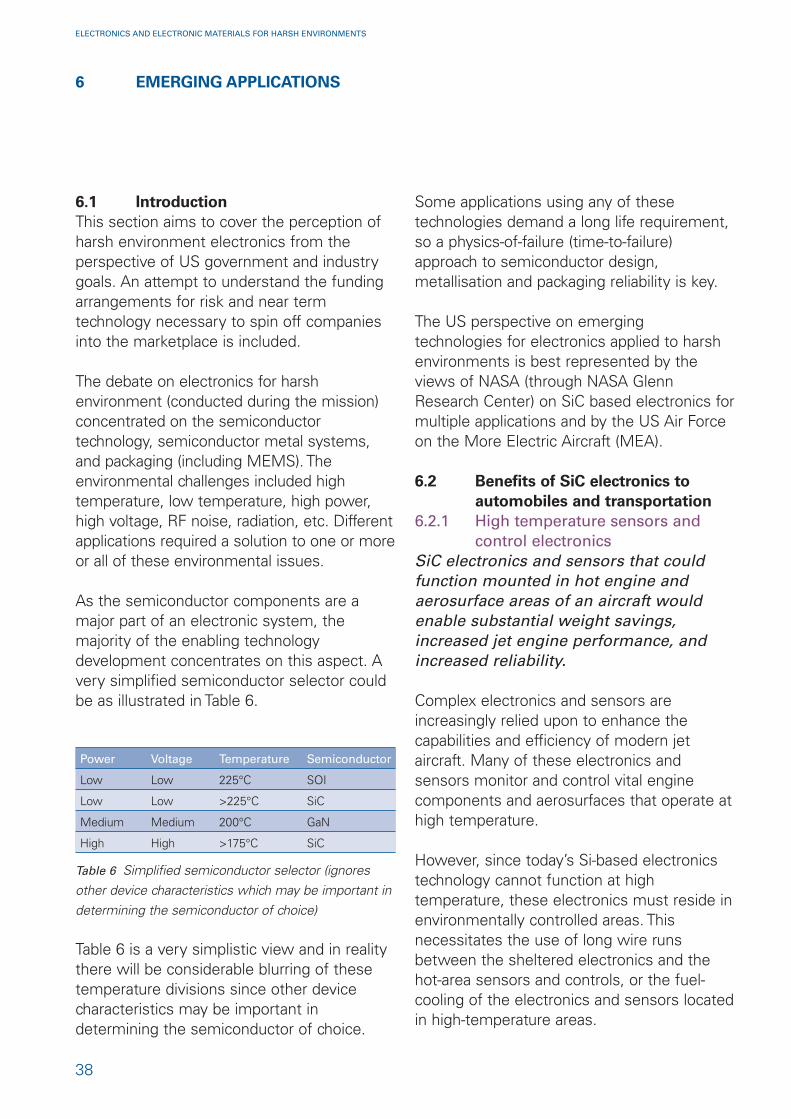
38
ELECTRONICS AND ELECTRONIC MATERIALS FOR HARSH ENVIRONMENTS
6 EMERGING APPLICATIONS
6.1 Introduction
This section aims to cover the perception ofharsh environment electronics from theperspective of US government and industrygoals. An attempt to understand the fundingarrangements for risk and near termtechnology necessary to spin off companiesinto the marketplace is included.
The debate on electronics for harshenvironment (conducted during the mission)concentrated on the semiconductortechnology, semiconductor metal systems,and packaging (including MEMS). Theenvironmental challenges included hightemperature, low temperature, high power,high voltage, RF noise, radiation, etc. Differentapplications required a solution to one or moreor all of these environmental issues.
As the semiconductor components are amajor part of an electronic system, themajority of the enabling technologydevelopment concentrates on this aspect. Avery simplified semiconductor selector couldbe as illustrated in Table 6.
Power Voltage Temperature Semiconductor
Low Low 225°C SOI
Low Low >225°C SiC
Medium Medium 200°C GaN
High High >175°C SiC
Table 6 Simplified semiconductor selector (ignoresother device characteristics which may be important indetermining the semiconductor of choice)
Table 6 is a very simplistic view and in realitythere will be considerable blurring of thesetemperature divisions since other devicecharacteristics may be important indetermining the semiconductor of choice.
Some applications using any of thesetechnologies demand a long life requirement,so a physics-of-failure (time-to-failure)approach to semiconductor design,metallisation and packaging reliability is key.
The US perspective on emergingtechnologies for electronics applied to harshenvironments is best represented by theviews of NASA (through NASA GlennResearch Center) on SiC based electronics formultiple applications and by the US Air Forceon the More Electric Aircraft (MEA).
6.2 Benefits of SiC electronics to
automobiles and transportation
6.2.1 High temperature sensors and control electronics
SiC electronics and sensors that couldfunction mounted in hot engine andaerosurface areas of an aircraft wouldenable substantial weight savings,increased jet engine performance, andincreased reliability.
Complex electronics and sensors areincreasingly relied upon to enhance thecapabilities and efficiency of modern jetaircraft. Many of these electronics andsensors monitor and control vital enginecomponents and aerosurfaces that operate athigh temperature.
However, since today’s Si-based electronicstechnology cannot function at hightemperature, these electronics must reside inenvironmentally controlled areas. Thisnecessitates the use of long wire runsbetween the sheltered electronics and thehot-area sensors and controls, or the fuel-cooling of the electronics and sensors locatedin high-temperature areas.

39
ELECTRONICS AND ELECTRONIC MATERIALS FOR HARSH ENVIRONMENTS
Both of these low-temperature-electronicsapproaches suffer from serious drawbacks, asthe wire runs add a substantial amount ofweight, fuel cooling has harmed aircraft fuelefficiency, and both have negatively impactedaircraft reliability.
A family of high temperature SiC electronicsand sensors that could function in hot areasof the aircraft would alleviate the above-mentioned technical obstacles to enablesubstantial aircraft performance gains.Uncooled operation of 300 to 600°C SiCelectronics and sensors would save weightand increase reliability by replacing hydrauliccontrols with ‘smart’ electromechanicalcontrols. SiC-based distributed controlelectronics would eliminate 90% of thewiring and connectors needed in conventionalsheltered-electronic aircraft control systems.
This is crucial given the fact that wiring andconnector problems are the most frequentcause of propulsion maintenance action anddowntime in commercial aircraft today. Evenin non-hot areas of an aircraft, SiC electronicswould enable the elimination of electronicscooling systems, such as the liquid coolingsystem employed in the F-22, that add weightand reduce operational reliability of high-performance aircraft.
SiC high temperature electronic sensorsand controls on an automobile engine willlead to better combustion monitoring andcontrol, resulting in cleaner burning, morefuel efficient cars.
Internal combustion automobiles areincreasingly relying on complex ‘under-the-hood’ electronics and sensors rated attemperatures from -40 to 125°C to meet thedemands for increasing fuel efficiency whiledecreasing pollutant emissions. Carefulplacement of Si-based engine controlelectronics boxes within the enginecompartment presently meets most oftoday’s automotive needs.
However, integrated SiC sensors functioningdirectly in contact with higher temperaturecylinder head and exhaust pipe areas wouldenable further gains in fuel combustionefficiency and reduced exhaust emissions.Furthermore, SiC-based engine controlelectronics rated at temperatures well above125°C would eliminate present-day boxplacement design constraints and wouldreduce the number of wires and connectorsin the engine, both of which should improvelong-term reliability.
6.2.2 Interference immunity of radio based avionics
Concern over the interference of stray RFemissions with key avionics is evidentduring takeoff and landing of everycommercial flight when the flightattendant requests that all portableelectronics be switched off.
The operation of key radio-based avionics (suchas glide-slope and localiser approachinstruments) depends on the ability of front-end RF receivers to detect and amplify desiredinformation signals while rejecting interferencefrom undesired RF sources both inside andoutside the aircraft. Incidents where keynavigation and approach avionics malfunctionbecause of RF interference clearly representan increasing threat to flight safety as the radiospectrum becomes more crowded.
In an initial feasibility experiment, ARL andthe NASA Lewis Research Center recentlydemonstrated the strategic use of SiCsemiconductor components to significantlyreduce the susceptibility of an RF receivercircuit to undesired RF interference. A pair ofSiC mixer diodes successfully reduced RFinterference (intermodulation distortion) in aprototype receiver circuit by a factor of 10 (20 dB) in comparison to a pair of commercialSi-based mixer diodes.
This can be seen by comparing the receivedsignal spectrum from a conventional Si-diode

40
ELECTRONICS AND ELECTRONIC MATERIALS FOR HARSH ENVIRONMENTS
mixer test circuit (Figure 14, left) with that froman SiC-diode mixer circuit (right). The twolargest peaks in the middle of both spectra arethe desired radio signals, which normallywould contain avionics-related information. Thepeaks to either side of the desired signal in thetop figure represent undesired intermodulationdistortion signals, which can interfere with theproper detection and decoding of desired radiosignals. The SiC-diode mixer circuit reducesthese interference peaks to the point wherethey cannot be observed in the spectrum ofthe figure on the right.
This circuit should enable avionics receiversto extract weak desired information signalsmuch more successfully, even in thepresence of strong undesired RFinterference. Such circuits would clearlyimprove the reliability of flight-critical radio-based instrumentation, even if passengerscontinued to operate portable electronicsduring takeoffs and landings. Furthermore,aviation-related RF transmitters and receiverscould be located closer to each other (both inthe air and on the ground) without severeinterference penalties.
Manufactured in volume, these simple-to-produce SiC mixers should cost around $10to $20 each, well below the $1,000 itpresently costs to achieve the same degreeof RF interference immunity from complex,series-matched mixer hybrid circuits.
6.2.3 High power electronics for electric vehicles
SiC will enable more practical electricvehicles and other transportation systemsby means of vastly improved powerelectronic devices.
The capabilities of electric vehicles are largelydetermined by the capabilities of the electriccircuits and motors that are responsible forconverting electrical energy into drivetrainenergy. Power semiconductor electronicdevices are key circuit elements whosecapabilities greatly influence motor-driveenergy conversion efficiency. Presently, thesedevices are all implemented in conventionalSi-based semiconductor technology.
Recent theoretical studies have shown thatonce SiC semiconductor technology becomessufficiently developed, SiC power devices willgreatly outperform Si power devices. In short,SiC power technology could operate at highertemperatures, stand off higher voltages, andswitch faster using devices that have lowerparasitic resistances and are physically muchsmaller than Si power devices. These highlydesirable device improvements wouldsubstantially trim the amount of undesirablepower losses in electric motor-drive powerconversion applications.
In addition to electric automobiles, superiorSiC power conversion electronics wouldenhance the performance of almost any form
Desired signal
Intermodulationinterference
Desired signal
Figure 14 Comparison of received signal spectra (attenuation 10 dB; RL 0 dBm) from conventional Si-diode mixercircuit (left) and SiC-diode mixer circuit (right – note the absence of intermodulation interference peaks)

41
ELECTRONICS AND ELECTRONIC MATERIALS FOR HARSH ENVIRONMENTS
of electric-motor transportation system, frommass transit trains and buses to commercialrailroad locomotives to commercial andmilitary surface ships and submarines.
6.3 Benefits of SiC electric power
systems
6.3.1 Energy savings in public power distribution
Superior SiC power electronics couldincrease the efficiency and reliability of thepublic electric power distribution system.
Today, utilities generate on average 20%more electricity than is consumed at anygiven time. This excess power reserve isneeded to ensure that electric service isreliably immune to everyday load changesand component failures that cause electricalglitches throughout the power grid.
The incorporation of solid state ‘smart’ powerelectronics into the power grid shouldsignificantly reduce the power reserve marginnecessary for reliable operation, because thesesemiconductor circuits can detect andinstantaneously compensate for local glitches. Ithas been estimated that a mere 5% reductionin power reserve margin would eliminate theneed for $50 billion worth of new power plantswithin the next 25 years. This same smartpower technology would also enable as muchas 50% larger power capacities to be carriedover existing powerlines.
Power semiconductor devices are a criticalelement of ‘smart’ power electronicstechnology. Presently, these devices are allimplemented in conventional Si-basedsemiconductor technology. Recent theoreticalstudies have shown that once SiCsemiconductor technology becomessufficiently developed, SiC power devices willgreatly outperform Si power devices. In short,SiC power devices could stand off highervoltages and respond faster using deviceswith lower parasitic resistances and physicalsizes much smaller than Si power devices.
Faster switching speed not only increasespower system conversion efficiency, but alsoenables the use of smaller transformers andcapacitors to greatly shrink the overall size andweight of the system. Furthermore, the hightemperature capability of SiC greatly reducescooling requirements that are also asubstantial portion of the total size and cost ofa power conversion and distribution system.SiC devices are therefore expected todrastically improve the distribution andefficient usage of electric power in the 21stcentury.
6.4 Benefits of SiC electronics to
commercial and planetary
spacecraft
6.4.1 Increased satellite functionality at lower launch cost
SiC high temperature electronics willreduce spacecraft launch weights andincrease satellite functional capacities.
Present-day commercial satellites requirethermal radiators to dissipate heat generatedby the spacecraft’s functional electronics.These electronics, currently based on Si orGaAs semiconductors, would fail if they werenot properly cooled by the spacecraft’sthermal radiators. Because SiC electronics canoperate at much higher temperature than Si orGaAs, the size and weight of such radiators ona spacecraft could be greatly reduced or eveneliminated. This would enable substantialweight savings on a satellite, or at least allowgreater functionality (ie more transponders ina communications satellite), by utilising thespace and weight formerly occupied by thethermal management system.
Furthermore, SiC electronic devices have alsobeen shown to be less susceptible toradiation damage than correspondingly ratedSi devices. SiC electronics could thereforealso reduce the size and weight of shieldingnormally used to protect spacecraft electroniccomponents from space radiation.
42
ELECTRONICS AND ELECTRONIC MATERIALS FOR HARSH ENVIRONMENTS
Given the exorbitant per pound costs oflaunching payloads into earth orbit, the weightsavings gained by using SiC electronics couldhave large economic and competitiveimplications in the satellite industry.
6.4.2 Solar system explorationSpacecraft with high temperature,radiation-hard SiC electronics will enablechallenging missions in both the inner andouter solar system.
Radiation-hard high temperature SiCelectronics will play a key role in futuremissions to the harsh environments near thesun and on the surfaces of the inner planets.Long-term operation of probes within Venus’sscorching 450°C atmosphere will require theuse of uncooled SiC electronics. For spacecraftoperating near the sun, SiC electronics wouldenable significant reductions in spacecraftshielding and heat dissipation hardware, sothat more scientific instruments could beincluded on each vehicle.
Space nuclear power will play a key role in theadvanced exploration of the outer solarsystem. Future space nuclear power systemswill require control and monitoring circuits forsafe and optimum reactor performance. Use ofheat-tolerant radiation hardened SiC circuitswill greatly reduce the shielding needed toprotect the reactor control electronics, andenable placement of the electronics in closeproximity to the reactor, both of which will trimconsiderable weight from the power system.
6.4.3 Advanced launch vehicle sensor & control electronics
SiC electronics and sensors that couldfunction mounted in hot engine andaerosurface areas of advanced launchvehicles would enable weight savings,increased engine performance, andincreased reliability.
Complex electronics and sensors are expectedto enhance the capabilities and efficiency of
advanced space launch vehicles. Many ofthese electronics and sensors monitor andcontrol vital engine components andaerosurfaces that operate at high temperature.
Since today’s Si-based electronics technologycannot function at high temperature, theseelectronics must presently reside inenvironmentally controlled areas. Thisnecessitates the use of long wire runsbetween the sheltered electronics and thehot-area sensors and controls, or fuel-coolingof the electronics and sensors located in high-temperature areas.
Both of these low-temperature-electronicsapproaches suffer from serious drawbacks, asthe wire runs add a substantial amount ofweight, fuel cooling has harmed launchvehicle fuel efficiency, and both havenegatively impacted launch vehicle reliability.
A family of high temperature SiC electronicsand sensors that could function in hot areas ofthe launch vehicle would alleviate the above-mentioned technical obstacles to enableperformance gains. Uncooled operation of 300to 600°C SiC electronics and sensors wouldsave weight and increase reliability byreplacing hydraulic controls with ‘smart’electromechanical controls. SiC-baseddistributed control electronics would eliminatewiring and connectors needed in conventionalsheltered-electronic control systems.
6.5 Benefits of SiC electronics to
communications and radar
6.5.1 High power, high temperature microwave RF electronic devices
SiC based microwave electronics canfunction at large power densities and hightemperatures offering significantimprovements to wirelesscommunications and radar.
The majority of solid state microwavecommunication and radar electronics ispresently implemented in GaAs

43
ELECTRONICS AND ELECTRONIC MATERIALS FOR HARSH ENVIRONMENTS
semiconductor technology. However, militaryaircraft desire solid state microwaveelectronics operating at higher powers andtemperatures than is theoretically possiblewith GaAs. SiC-based microwave electronicsis being developed to fill this void, but manyof the same performance advantages apply tothe expanding ‘global village’ of worldwideelectronic wireless communications.
Even though SiC technology is relativelyyoung and immature compared to well-developed GaAs technology, the superiorinherent physical properties of SiC havealready enabled prototype SiC transistors toperform at power densities well beyond thetheoretical limit of GaAs-based microwavetransistors. SiC RF transistors are expected tobe incorporated into radar systems, cellphone base stations, and high definitiontelevision (HDTV) transmitters in the nearfuture.
6.6 Air Force perspective of SiC
A revolutionary transformation in aircraftelectrical power technologies is under waythat promises the Air Force greater aircraftreliability and a significantly smaller logisticaltail to support tomorrow’s air and space force.The more electric aircraft (MEA) is becominga reality thanks to improved powertechnologies.
The proof is in the F-35 Joint Strike Fighter(JSF), which incorporates technologiesenvisioned, designed, developed and testedby a large collaborative team involving bothUS and non-US governmental agencies,universities, and aerospace industry partners.
The MEA concept involves using electricalpower to drive aircraft subsystems that arecurrently powered by hydraulic, pneumatic ormechanical means. This includes gearboxes,hydraulic pumps, electrical generators, flightcontrol actuators, and other aircraftsubsystems. New concepts like electricenvironmental control and electric fuel
pumps, along with magnetic bearings forgenerators and eventually more electricturbine engines, are planned for the future.They promise dramatic simplifications inaircraft system design, while improvingreliability and maintainability.
MEA systems involve the evolutionaryapplication of electrical power systems,electronics, and distributed architectures tosimplify much of the current bulk andcomplexity inherent in hydraulic andpneumatic aircraft systems. Immediatebenefits derived from the wider application ofelectrical power and electronics include betterperformance as well as savings in weight,space, and overall life-cycle costs.
A variety of technologies had to be matured tobuild this type of aircraft, from more powerfulstarter/generators for turbine engines toadvanced batteries (eg rechargeable lithiumbatteries) which provide very high energydensity and high power with low weight.
A full operating-speed demonstration of anintegrated power unit (IPU) rotor system atspeeds in excess of 61,000 rpm has beenrealised. The IPU is being developed byHamilton Sundstrand, under sponsorship ofthe Propulsion Directorate of the US Air Force(USAF), and uses magnetic bearings ratherthan traditional lubrication systems. Thedesign, based on the elimination of thelubrication system alone, is projected toreduce maintenance by more than 50% overconventional designs, with expected energysavings of up to 30%.
Another successful demonstration is theelectric flight control system, or power-by-wire, incorporated into the F-35. As part ofthe JSF demonstration programme, electricactuators, or motors, replaced hydraulics in anAdvanced Fighter Technology Integration F-16tested at Edwards Air Force Base, California.The testing proved that electric flight controlscould be transparent to the pilot.

44
ELECTRONICS AND ELECTRONIC MATERIALS FOR HARSH ENVIRONMENTS
7 R&D FUNDING
7.1 Introduction
The emphasis in many programmes andorganisations within the US is oncollaboration and looking to governmentagencies to support development and istypified by NASA Glenn Research Center.
7.2 NASA Glenn
The NASA Glenn High Temperature IntegratedElectronics and Sensors (HTIES) team remainsin a unique position to make crucialcontributions to the fledgling SiC industry in theUS. In particular, it has the unique resources andknowledge needed to conduct revolutionary SiCresearch that is beyond the short-term low-riskplans of profit-driven industry.
The NASA Glenn HTIES team has a proventrack record of transferring important SiCtechnologies to US industrial customers. Thebase technology developed by NASA Glennfor epitaxial growth of SiC has become awidely accepted industry standard. Theimportance and relevance of NASA Glennresearch to US industry by providing advancedSiC technology is reflected in past and presentcollaborative efforts with companies,institutions, and government laboratories.
To maximise the impact of every taxpayerdollar spent on SiC research, NASA Glenn isor has been involved in fruitful joint researchprojects with the following US governmentlaboratories:
• Air Force Research Laboratory (AFRL)• Army Research Laboratory (ARL)• Defense Advanced Research Projects
Agency (DARPA) • NASA Jet Propulsion Laboratory (JPL)• Naval Research Laboratory (NRL)• Office of Naval Research (ONR)
Networking of government funding agenciesand research laboratories seems to havereached a productive level. Money spent istargeted at key technologies for demandedharsh environment applications. Theapplications are generated from the needs ofgovernment agencies, national security,environmental requirements, andindustrial/economic development. The moneyfunds technology development to andincluding near market production status.
Although research laboratory networkingdoes take place, each laboratory has a budgetto pursue a custom requirement in harshenvironment technology. University fundingand industrial partnerships add to thispowerful network.
7.3 Joint industrial partnership (JIP)
The most significant development incommercial SOI development in the US is the joint industrial partnership (JIP) led byHoneywell and part funded by the USgovernment’s DeepTrek programme.
DeepTrek is an initiative of the USDepartment of Energy (DOE), the NationalEnergy Technology Laboratory (NETL) and theStrategic Center For Natural Gas (SCNG). Theaim is to develop technology to dramaticallyreduce the cost/risk of drilling to depths of20,000 ft or more.
The objective of the DeepTrek hightemperature electronics programme is toprovide a solution for the gap in the downhole industry for a functional suite of hightemperature electronic components which canbe used for high temperature instrumentationin the gas and petroleum deep well domainand other smart well applications. One of thereasons for this gap is the reluctance of

45
ELECTRONICS AND ELECTRONIC MATERIALS FOR HARSH ENVIRONMENTS
component manufacturers to invest in newproduct lines absent a reasonable assuranceof a viable market. Conversely, the gas andpetroleum industry needs reasonableassurance that a full suite of compatiblecomponents will be commercially availableand usable in industry deep well applications.
This technology also has spin-off potential toother high temperature markets (eg industrialand/or aerospace control systems), andenables electronic controls anywhere thattemperature is a roadblock. GoodrichAerospace Engine Control Systems UK aremembers of the JIP team and are inputtingan aerospace perspective into componentdevelopment, for example -55°C operationand long life at high temperature.
Commercialisation of SOI electronics forharsh environments can now be attained by:
1 The JIP membership identifying systemlevel electronics specifications for productsthat need commercialisation;
2 DOE and JIP industry membership fundingthe high temperature development; and
3 Honeywell Solid State Electronics Center(SSEC) of Excellence developing the hightemperature technology andcommercialising the system level products.
7.4 Benefits to industry
High reliability, high temperature electronicproducts and technology will enable smartdrilling at depths of 20,000 ft. Making thedrilling process ‘smarter’ will improve drillingefficiency and success rate. Without suchtechnology, deep energy assets will likelycontinue to be out of reach because oftechnical and economic barriers.
This programme will benefit down-hole wellservice companies, enabling them to expandinto applications that have been technicallyout of reach. It will provide them with
electronic standard products. Just asimportant, it will provide access to hightemperature technology on a foundry andapplication-specific-integrated-circuit (ASIC)basis, thereby allowing use of thetechnology while preserving proprietaryapproaches and product differentiation. Thiswill ultimately result in the availability ofmore tools and systems to support thedeep-drilling mission.
Producer companies will benefit fromdevelopment of rugged high-temperaturetools and telemetry systems. The technologywill have reliable operation for five years at225°C, opening the way for permanentinstallation of electronics in completed wells.Additionally, at lower continuoustemperatures of 175°C there is an expectedlife of 10 to 15 years. This enables longer lifefrom permanent gauging, hence moreefficient production. (The life targets forpermanently installed wells match thoserequired by the aerospace market). Theprogramme may also encourage standardsfor down-hole interconnectivity, protocols,and telemetry means for down hole.
Finally, the US economy and strategic nationalinterests benefit by unlocking domesticenergy assets that are now beyond reach.This will lessen US reliance on foreignsources and strengthen the economy.
7.5 Methodology to achieve
objectives
SSEC, also corporately identified as Defenceand Space Electronic Systems Plymouth, hashigh temperature (225°C continuous duty forfive years) commercialised electronics that itpresently distributes through its worldwidesales and marketing organisation. SSECproposes taking its existing 0.8 micron, 5 volthigh temperature SOI process and addinghigh temperature SOI mixed signal capabilitythrough an upgrade of its existing 125°Cmixed signal design cell libraries to 225°C.

46
ELECTRONICS AND ELECTRONIC MATERIALS FOR HARSH ENVIRONMENTS
The high temperature SOI mixed signalprocess once developed and characterisedwill also have design toolkits and library.These will be used first to design aborecleaner to demonstrate functionalcapability to debug the high temperature SOImixed signal process.
Proposed products to be fabricated on thehigh temperature mixed signal process are: a16 bit analogue-to-digital (A/D) converter; aprecision operational amplifier; a serialcommunications interface; and amicrocontroller. Additionally, a pressuretransducer instrument demonstration isplanned by the integration of the developed225°C electronics products with a hightemperature pressure sensor. SSEC is alsoproposing to upgrade its 0.35 micron, 125°CSOI digital process to a 225°C hightemperature process and use this to developa field programmable gate array (FPGA).
Continued development and creation ofnew/next generation high temperature SOIASIC system level instrumentation electronicswill be facilitated by the use of SSEC’s hightemperature mixed signal design toolkits inconjunction with SSEC’s high temperatureSOI mixed signal process.
Honeywell make high temperature SOIcircuits based on their radiation hardened SOIprocess. Their high temperature technologyrange comprises both 5-volt digital and 10-voltanalogue devices, but the economics ofproducing the latter in a low volume markethave become difficult.
The DeepTrek programme funded by the DOEand industrial partners will result in ASIC andFPGA based component production. Thetechnology will be 5-volt digital and mixed signalASIC and 3.3-volt FPGA. Using special barrierlayers under the aluminium on thesemiconductor die the migration life has beenincreased. The components will be specified as44,000 hours at 225°C, 90,000 hours at 200°C
and 130,000 hours at 180°C. Failure is definedas 10% increase in die metal resistance.
The bulk silicon market is moving in thewrong direction for life and harsh environment applications; this is also true forcommercial SOI. Harsh environment SOIrequires adjustment to many parameters andthis can be seen in Table 7.
Honeywell device technology is based onpartially depleted SOI. Researchers aredeveloping fully depleted SOI for harshenvironments and believe that performance ispossible up to 300°C and life is possible if thedie metal is changed to tungsten gold (oranother metal structure).
Issue Primary mitigation strategies
Junction leakage SOI process
Sub-threshold Vt adjustmentleakage
Electromigration Design rules to lower maximum current density
Reduced mobility Design adjustments:Temp. compensated biasingLarger digital devices or derate clock frequency
Bias voltage drift Design techniques (eg ZTC biasing)with temperature
Self-heating Design for lower power density, layout floorplanning, metal-interconnect heat-spreading etc
Floating body Partially-depleted SOI with body tieeffects Layout rules for max spacing to
body-tie contacts
Back-gate Increased back-oxide thicknesstransistors
Table 7 Mitigation strategies for issues in harshenvironment SOI (Honeywell)

47
ELECTRONICS AND ELECTRONIC MATERIALS FOR HARSH ENVIRONMENTS
8 CONCLUSIONS AND
RECOMMENDATIONS
This report gives an overview of the trendsand developments of electronics andelectronic materials for harsh environmentsfollowing visits and extensive discussionswith a number of prime movers in the US.The organisations visited represent a crosssection of users and suppliers from originalequipment manufacturers (OEMs) to smalland medium enterprises (SMEs), national labsand university research groups.
The use of electronics in harsh environmentsis to some extent still embryonic, particularlyin high temperature environments. However,high temperature exploitation of advancedelectronic systems is becoming critical for anumber of key market applications such asdeep oil & gas wells, geothermal, and moreelectric technologies in the automotive andaerospace sectors.
It is clear that the US enjoys a premier positionin the global market as the leader in widebandgap (WBG) semiconductor substrateprovision. It is also home to the only trulycommercial source of high temperature silicon-on-insulator (SOI) components. The workinstigated through Glennan Microsystems Inc(GMI) and NASA Glenn Research Center hasalso begun to reap dividends in the field ofrobust high temperature and hostileenvironment microsystems.
The mission members drew the followingmajor conclusions:
• There are strong interests in both the UKand the US to exploit electronics in harshenvironments. In fact there is a criticalneed in UK companies for reliableelectronics for operation at elevatedtemperatures and/or high powers.
• The level of investment for the developmentof electronics for harsh environments in theUS far outstrips that available to the UKalone or even European-wide investment.The main historical driver in the US hasbeen its internal defence requirements,although significant investment is nowbeing diverted from the energy sector.
• A wealth of different mechanisms havebeen exploited to fund start-up companiesin the field of WBG semiconductors in theUS. However, these companies have allbenefited from extensive governmentresearch contracts placed mainly throughDepartment of Defense (DOD) agencies.
• The commercialisation of WBGsemiconductor materials – silicon carbide(SiC) and gallium nitride (GaN) – is faradvanced in the US. Cree is theacknowledged world leader in the supplyof SiC substrates.
• The UK has no commercially activecompanies in SOI, SiC or GaN.
• The UK has research activities in GaN andSiC but these generally fall short of USdevice work although in some areas offundamental research the UK iscompetitive with the US.
• Europe (eg Siemens) is competitive with theUS in SiC high power/voltage technology.
• In microwave technology (both SiC andGaN) the US is far in advance of the UKand is protecting this position via exportcontrols (International Traffic in ArmsRegulations – ITAR).

48
ELECTRONICS AND ELECTRONIC MATERIALS FOR HARSH ENVIRONMENTS
• Europe (eg Osram) is competitive with theUS in some optoelectronic devices.
• Neither the US nor the UK has significantprogrammes in packaging for harshenvironments or in studying longer termreliability of systems and devices for harshenvironments.
• There is strong bilateral desire tocollaborate in developing technologies forharsh environments.
Given the lead that the US has alreadydemonstrated in WBG semiconductor substratedevelopment, particularly in SiC, and given thecost to develop this technology, the UK shouldconcentrate on where it can add value. The UKhas a well developed GaN community and thisshould continue to be competitive if supportcontinues. However, there are no signs withinthe UK of the emergence of an indigenouscommercial supplier of GaN substrate materials,whereas several companies in the US arebeginning to market products.
UK companies should be encouraged tocollaborate with US organisations. There wasa genuine willingness to be cooperative, withmost of the hosts visited being frank andopen about their future developmentstrategies. The collaborative researchundertaken on a pan-European scale throughthe European Union (EU) Frameworkprogrammes was seen as a great advantageover the US system, where such multi-institutional research is less common.
The principal recommendation of themission team is that the UK should focuson device development and packaging andreliability for harsh environments.
Nevertheless, SOI, SiC and GaN devices willbe required for a full harsh environmentsystem. Unless the cost of these devices canbe reduced the technologies for harshenvironments will remain low volume. Selling
these devices only makes business sense ifthey are supplied worldwide from a fewsuppliers (for example Honeywell is only ableto develop their high temperature product lineby modifying their existing radiation-hardtechnology – they would not be able to affordto develop a high temperature electronicsbusiness from scratch). If the cost can bereduced then the same devices could beused in high reliability systems (non harshenvironment), thus increasing the volume.
Even the US market for these technologies isnot driving device manufacturers to producecomponents for a full system. In addition thedevelopment is not resulting in a robustsupply of devices in the marketplace.Consider the following:
• 99% of Cree wafers will be used by Cree,therefore single source devices. The USand world market will determine the Creedevice road map but harsh environmentmay not be the major driver.
• The same route may also emerge for GaN.
• The new policy of Honeywell is to becomethe only supplier of high temperature longlife SOI devices. The US gas & oil sectorwill determine the Honeywell road mapand there is not enough funding forHoneywell to produce a full range of parts.
• The US is developing the technology thatcould be used for harsh environments butthe drive to make a business that suppliesthe world market with a full range ofproducts is as far away as it has always been.
If the UK or EU could progress their SOIand/or SiC and/or GaN device manufacture inorder to create device fabs dedicated to theharsh and high reliability marketplace thenthis would capture the business andguarantee a reliable indigenous source for theUK in this strategic niche market.

49
ELECTRONICS AND ELECTRONIC MATERIALS FOR HARSH ENVIRONMENTS
Appendix AMISSION PARTICIPANTS
Organisation ALSTOM Research & Technology (ART) Centre
Contact Roger J Bassett PhD, MTech, FIEE, MInstP
Position Technology Consultant, Power Electronics/Devices
Organisation size 60 people at ART Centre serving ALSTOM’s 100,000 people in 70 countries
Address PO Box 30Lichfield RoadStaffordStaffordshireST17 4LNUK
Tel 01785 274 986
Fax 01785 274 676
Email [email protected]
Web www.alstom.com
Platform technologies • High voltage – 10 to 100 kV – and high EMC stress applicationsfor harsh environment • High temperature so we can use very small devices with very
small heat sinks, therefore cheap equipment cost, in electricity supply distribution systems and transmission of electricity in cities, eg where space power cabling is limited
• Very long life – 30 years or more
Areas for potential • Device developmentcollaboration for harsh • Application packaging developmentenvironment • Strategies for zero cooling
• Ruggedisation of new technologies for high power and/or high temperature operation

50
ELECTRONICS AND ELECTRONIC MATERIALS FOR HARSH ENVIRONMENTS
Organisation Faraday Advance and Oxford University, Department ofMaterials
Contact Colin Johnston PhD, BSc (Hons), MRSC
Position Technology Translator and Senior Research Fellow
Organisation size The University employs 7,300 staff of which 3,700 are academics. There are 16,500 residential students. The Department of Materials has 300 members, consisting of 24 academics, 16 senior researchers, 51 postdoctoral researchers, 38 technicians and administrative staff, 33 academic visitors, 92 research students and101 undergraduates.
Address Department of MaterialsOxford University Begbroke Science ParkSandy LaneYarntonOxfordshire OX5 1PFUK
Tel 01865 283 705
Fax 01865 848 790
Email [email protected]
Web www.faraday-advance.netwww.materials.ox.ac.uk
Platform technologies High temperature electronics, especially:for harsh environment • Passive component technology, especially capacitors, inductors
and resistors• Packaging technology – ceramic and polymeric• Thick and thin film processing
Areas for potential • Lifing and failure mode analysis prediction for high temperaturecollaboration for harsh • Materials analysisenvironment • Materials integration at elevated temperature
• Packaging for high temperature operation

51
ELECTRONICS AND ELECTRONIC MATERIALS FOR HARSH ENVIRONMENTS
Organisation QinetiQ Ltd
Contact Michael J Uren PhD, CPhys, FInstP
Position QinetiQ Fellow and Team Leader, High Power Devices
Organisation size 8,000 employees
Address St Andrews RoadGreat MalvernWorcestershireWR14 3PSUK
Tel 01684 894 404
Fax 01684 895 774
Email [email protected]
Web www.qinetiq.com
Platform technologies • SiC and GaN WBG devicesfor harsh environment
Areas for potential • WBG devicescollaboration for harshenvironment

52
ELECTRONICS AND ELECTRONIC MATERIALS FOR HARSH ENVIRONMENTS
Organisation BAE SYSTEMS Advanced Technology Centre (ATC)
Contact Nick Chandler BSc (Hons) Physics, PhD Solid State Physics
Position Senior Principal Scientist, Deputy Head of Department, Sensor Technology
Organisation size BAE SYSTEMS worldwide: >120,000 employees BAE SYSTEMS ATC: ~500; at this site: ~250
Address West Hanningfield RoadGreat BaddowChelmsfordEssexCM2 8HNUK
Tel 01245 242 895
Fax 01245 242 405
Email [email protected]
Web www.baesystems.com
Platform technologies BAE SYSTEMS is a leading systems company innovating for a safer for harsh environment world, delivering total solutions to customer requirements. With a
major presence internationally, particularly in Europe and the USA, it designs, manufactures and supports military aircraft, surface ships, submarines, space systems, radar, avionics, C4ISR, electronic systems, guided weapons and a range of other defence products, many with international partners. The Advanced Technology Centre (ATC) provides innovation, expertise and services for the creation and development of future technology capabilities covering a broad spectrum: from hardware to software development, sensing systems to synthetic environments. With a highly skilled scientific workforce, ATC provides support throughout the product life cycle, from longer term speculative research to applied product development.
Areas for potential ATC works with external organisations including the UK MOD,collaboration for harsh US DOD, ESA, universities, etc. Topics of key interest relating to environment harsh environments include:
• Design and manufacture of digital, analogue and microwave modules, to reduce size and weight
• Design and manufacture for applications using devices able to run at high temperatures, to minimise cooling requirements
• Ruggedisation of optical and optoelectronic modules and assemblies
• Application of novel/emerging materials and techniques to any ofthe above
53
ELECTRONICS AND ELECTRONIC MATERIALS FOR HARSH ENVIRONMENTS
Organisation Goodrich Engine Control Systems
Contact Peter Shrimpling BSc (Hons) Electrical & Electronics
Position Harsh Environment Advanced Electronic Product Specialist
Organisation size 2,000 employees (part of parent company Goodrich Control Systems)
Address York RoadHall GreenBirminghamWest MidlandsB28 8LNUK
Tel 0121 627 6600
Fax 0121 607 3658
Email [email protected]
Web www.goodrich.com
Platform technologies Electronic product with embedded software supporting sensors for harsh environment and in-house fueldraulic actuation applied to jet engine full authority
digital electronic control. Demonstration of high temperature distributed electronic product installed in the actuator-sensor housing (smart actuators – mechatronics).20 kW more electric fly-by-wire flight surface actuation and control.100 kW more electric pump with power drive and control electronics demonstration. More electric primary and secondary power conversion and distribution.
Areas for potential • Applying advanced semiconductor technology (SOI, SiC, GaN collaboration for harsh etc) to system challenges.environment • Design and manufacture of high temperature low power
advanced MCM products.• High power motor, motor drive and control electronics design
and application.• More electric power stage packaging.• Fueldraulic (low power) and more electric (high power) smart
actuator demonstration.

54
ELECTRONICS AND ELECTRONIC MATERIALS FOR HARSH ENVIRONMENTS
Organisation QuantX Wellbore Instrumentation
Contact Iain Maclean BA, CEng MIEE, Cert Mgmt
Position Engineering Manager
Organisation size 100 employees
Address Wallace BuildingKirkhill PlaceKirkhill Industrial EstateDyceAberdeenAB21 0GUUK
Tel 01224 214 802
Fax 01224 214 791
Email [email protected]
Web www.quantx.com
Platform technologies Electronics & sensors for control and data acquisition as used for infor harsh environment well permanent monitoring for the oil and gas industry.
Areas for potential Materials, semiconductor and device design and manufacturecollaboration for harsh (SiC, SOI) for high temperature sensors.environment Reliability for high temperature electronics

55
ELECTRONICS AND ELECTRONIC MATERIALS FOR HARSH ENVIRONMENTS
Organisation EPPIC Faraday Partnership
Contact Robin Young PhD
Position Technology Translator
Address c/o TWI LtdGranta ParkGreat AbingtonCambridgeCB1 6ALUK
Tel 01223 891 162
Fax 01223 891 284
Email [email protected]
Web www.eppic-faraday.com
Platform technologies TWI is a worldwide recognised centre for materials, joining and for harsh environment assembly technology. Services range from product design
assistance through development of materials and processes to the assessment of manufacturing systems, production line troubleshooting and staff training.
Areas for potential EPPIC Faraday Partnership seeks to focus the electronics collaboration for harsh and photonics packaging research activities in the UKenvironment

56
ELECTRONICS AND ELECTRONIC MATERIALS FOR HARSH ENVIRONMENTS
Organisation Pera Innovation Limited
Contact David Jack BSc (Hons) Physics, MBA
Position International Technology Promoter (ITP)
Organisation size 150 employees
Address Pera Innovation ParkMelton MowbrayLeicestershireLE13 0PBUK
Tel 0141 584 9585
Fax 01664 501 261
Email [email protected]
Web www.globalwatchonline.com/itp
Areas for potential The International Technology Promoter (ITP) Programme, funded bycollaboration for harsh UK Department of Trade and Industry (DTI), facilitates internationalenvironment partnerships between companies, research organisations and
intermediary organisations in the UK and specific other countries(including USA and Canada). It offers access to leading edge technology developments from the world’s major investors in R&Dthrough a network of technology transfer specialists

57
ELECTRONICS AND ELECTRONIC MATERIALS FOR HARSH ENVIRONMENTS
Appendix BHOST ORGANISATIONS
Technologies & Devices International (TDI) Inc 20 Oct 0830Vladimir Dmitriev, President and CEOTDI Inc was founded in 1997 to commercialise basic R&D in crystal growth and devicefabrication of WBG semiconductors. It is developing bulk crystals, epitaxial structures anddevices over a range of materials with applications in short wavelength optoelectronicsand high power semiconductor electronics.
TDI develops, manufactures and markets electronic components using SiC and III-V nitridesemiconductor materials, and has started the commercialisation of SiC epitaxial wafers,GaN/sapphire and GaN/SiC epitaxial wafers. It is currently supplying these products tocustomers in the US, Japan, Europe and Australia. www.tdii.com
Computer Aided Life Cycle Engineering (CALCE) Electronic Products & Systems Center (EPSC), University of Maryland 20 Oct 1045
Prof Michael Pecht, Chair Professor & DirectorCALCE EPSC is recognised as a founder and driving force behind the development andimplementation of physics-of-failure approaches to reliability and life cycle prediction, aswell as a world leader in accelerated testing, and electronic parts selection andmanagement. It is at the forefront of international standards development for criticalelectronic systems, having chaired the development of several reliability and part selectionstandards.
CALCE EPSC is staffed by over 100 faculty, staff and students, and in 1999 became thefirst academic research facility in the world to be ISO 9001 certified. Collectively, CALCEresearchers have authored over 25 internationally acclaimed textbooks and well over 250research publications relevant to electronics reliability. Over the last 15 years, CALCEEPSC has invested over $50 million in developing methodologies, models, and designtools that address the design and manufacturing of electronic systems.www.calce.umd.edu

58
ELECTRONICS AND ELECTRONIC MATERIALS FOR HARSH ENVIRONMENTS
Naval Research Laboratory (NRL) and Army Research Laboratory (ARL) Workshop 20 Oct 1345
Dr Denis C Webb, Head, Microwave Technology Branch, NRLDr Pankaj B Shah, Sensors and Electron Devices Directorate, ARLNRL is the corporate research laboratory for the Navy and Marine Corps and conducts abroad programme of scientific research, technology and advanced development. NRL hasserved the Navy and the nation for 80 years and continues to meet the complextechnological challenges of today's world.
ARL plays a key role in DOD and Army R&D programmes. Six technology divisions –sensors and electron devices, computational and information sciences, weapons andmaterials research, human research and engineering, survivability/lethality analysis, andvehicle technology – are helping the US Army combat today’s challenges facing themodern soldier.www.nrl.navy.milwww.arl.army.mil
NASA Glenn Research Center 21 Oct 0900Dr Phil Neudeck, Silicon Carbide Electronics EngineerThe Glenn Research Center mission is to work as a diverse team in partnership withgovernment, industry and academia to increase national wealth, safety and security,protect the environment, and explore the universe. Glenn develops and transfers criticaltechnologies that address national priorities through research, technology developmentand systems development for safe and reliable aeronautics, aerospace and spaceapplications.
Glenn leads NASA R&D in aeropropulsion – powering flight through the atmosphere andbeyond. The Center's aeropropulsion programme plays a significant role in NASA's goalsto promote economic growth and national security through safe, superior andenvironmentally compatible US civil and military aircraft propulsion systems. Major effortsare in subsonic, supersonic, hypersonic, general aviation and high-performance aircraftpropulsion systems as well as in materials, structures, internal fluid mechanics,instrumentation and controls, interdisciplinary technologies, and aircraft icing research.
The Center also designs power and propulsion systems for space flight systems insupport of NASA programmes such as the International Space Station, Mars Pathfinder,and Deep Space 1. Glenn also leads NASA's Space Communications Programme includingthe operation of the Advanced Communications Technology Satellite (ACTS). www.grc.nasa.gov

59
ELECTRONICS AND ELECTRONIC MATERIALS FOR HARSH ENVIRONMENTS
Case Western Reserve University (CWRU) 21 Oct 1300Dr Mehran Mehregany, Department Chair Electrical Engineering and Computer Science;Goodrich Professor of Engineering InnovationOne of the most respected US universities. The Department of Engineering has an activeprogramme in semiconductor materials and devices, including research on:• Design, modelling, fabrication and testing of microsensors • Microactuators and related micro-electro-mechanical systems• Micro-opto-mechanical devices including optical scanners and micro-optical switches
and switch arrays• SiC materials, processing and device research• Electronic devices in mobile communication circuits• Microfabrication and IC process developmentwww.cwru.edu
Glennan Microsystems Inc (GMI) 22 OctDr Walter Merrill, Executive DirectorGMI was founded in 1998 as an Ohio-based, public-private partnership (GlennanMicrosystems Initiative). Named for T Keith Glennan, the first administrator of NASA and aformer president of CWRU, GMI focuses on physical sensors, chemical sensors andactuators in harsh environments.
GMI leverages the R&D capabilities and application interests of partners such as NASAGlenn Research Center, CWRU, other academic institutions, industry and government.GMI's purpose is to assist technology companies by providing for research, developmentand commercialisation of microsystems technology.www.glennan.org
Ford Motor Company 22 OctRichard E Soltis, Senior Technical Specialist, Physical and Environmental SciencesDepartmentFord runs a scientific research laboratory in Dearborn, Michigan where strategic researchis performed on safety, engines and emissions, design and manufacturability.www.ford.com
GE Global Research 22 OctThis world-class technology centre is spread over a dozen buildings in upstate New Yorkand employs more than 1,600 people. Multidisciplinary teams are assembled to developtechnologies in areas like electronic systems, manufacturing and business processes.www.crd.ge.com

60
ELECTRONICS AND ELECTRONIC MATERIALS FOR HARSH ENVIRONMENTS
Cree Inc 23 Oct 0900Mark Parrish, Corporate Accounts ManagerCree develops and manufactures semiconductor materials and devices based on SiC, GaN,Si and related compounds. The company’s products include blue, green and UV LEDs, nearUV lasers, RF and microwave devices, power switching devices and SiC wafers sold forproduction and for use in R&D. Targeted applications for these products include solid stateillumination, optical storage, wireless infrastructure and power switching.www.cree.com
Center for Advanced Vehicle Electronics (CAVE), Auburn University 24 Oct 0900Prof Wayne Johnson, Alumni Professor of Electrical & Computer EngineeringCAVE is dedicated to working with industry in developing and implementing newtechnologies for the packaging and manufacturing of electronics with special emphasis onthe cost, harsh environment and reliability requirements of the vehicle industry. Staff workdirectly with the member companies to identify challenges and opportunities for newmaterials, processes and approaches to the production of electronics. The membercompanies select the research projects. Semi-annual project reviews, visits, monthlyupdates and frequent phone calls maintain a close interaction between the industrialmembers and CAVE researchers.http://cave.auburn.edu
Nitronex Corp 23 Oct 1300Jim Vorhaus, Chief Operating OfficerNitronex is an emerging leader in the global wireless communications market. Driving thecompany’s successes are its premier financial backers and experienced seniormanagement team. When combined with unparalleled technology and a market thatrequires fundamental change, Nitronex is attracting worldwide attention and helping makeNorth Carolina and the Research Triangle Park area an international epicentre for GaN andwireless efforts.
Since licensing initial technology from North Carolina State University, a world leader inWBG and compound semiconductor research, Nitronex has received more than $45million in funding from preeminent leaders in semiconductors and RF communications. In2001, Nitronex was one of the best-funded private companies in the state of NorthCarolina, receiving the North Carolina Electronics and Information TechnologiesAssociation’s ‘Top Venture Capital Invested Company of the Year’ award.
Key investors include: TPG Ventures, the venture capital arm of Texas Pacific Group;Vantage Point Venture Partners, ranked among the top VC firms in the nation; and AllianceTechnology Ventures, an early investor in some of the industry’s most successful RFcompanies. All three firms are actively involved in contributing to Nitronex’s success.www.nitronex.com
61
ELECTRONICS AND ELECTRONIC MATERIALS FOR HARSH ENVIRONMENTS
Alabama Microelectronics Science & Technology Center (AMSTC), Auburn University 24 Oct 1200
Prof Richard Jaeger, Distinguished University ProfessorThe original Microelectronics Laboratory at Auburn University was established in theElectrical & Computer Engineering Department in 1974. In 1984, AMSTC was formed,following a special legislative appropriation of $250,000/year for support ofmicroelectronics through the Auburn University Engineering Experimental Station (this hasincreased to roughly $300,000/year currently). These funds are currently being used forgraduate student support, operating expenses, laboratory facilities enhancement, and forrecruiting and retaining faculty.
The Center's goal is ‘to advance microelectronics education and technology’ by providingfacilities that encourage research and educational activities within the University. AMSTCis interdisciplinary, bringing together the expertise necessary to address the multi-facetedtechnologies of microelectronics
Auburn University has been active in SiC research since 1989. Research efforts betweenthe Electrical & Computer Engineering and Physics Departments include developing ohmiccontacts, epitaxial growth of SiC, oxide/insulator studies, device fabrication andcharacterisation over wide temperature ranges, reactive ion etching of SiC, hybrid SiCcircuit fabrication, testing and design, high temperature, high power and high frequencypackaging, as well as SiC/nitride heterostructure device development.
Auburn's primary research partners in SiC are industrial partners in the Center forCommercial Development of Space within the NASA Space Power Institute at AuburnUniversity. A close relationship with companies such as Westinghouse provide Auburnwith insight into key problems which must be solved, and the alliance has proven fruitfulfor both Auburn and its industrial partners.http://spider.eng.auburn.edu/amstc/main/index.htm

62
ELECTRONICS AND ELECTRONIC MATERIALS FOR HARSH ENVIRONMENTS
Appendix CLIST OF ABBREVIATIONS
µm micrometreA ampere (amp)ACPR adjacent channel power ratioAFRL Air Force Research Laboratory (US)Ag silverAl aluminiumAlGaN aluminium gallium nitrideAlN aluminium nitrideAMSTC Alabama Microelectronics Science &
Technology Center (Auburn University)ARL Army Research Laboratory (US)ASIC application-specific integrated circuitAu goldBICMOS bipolar CMOSBJT bipolar junction transistorBPD basal plane dislocation°C degrees CelsiusCALCE Computer Aided Life Cycle Engineering
(Electronic Products & Systems Center,University of Maryland)
CAVE Center for Advanced VehicleElectronics (Auburn University)
cm centimetreCMOS complementary metal oxide
semiconductorCr chromiumCTE coefficient of linear thermal expansionCu copperCVD chemical vapour depositionCWRU Case Western Reserve UniversityDARPA Defense Advanced Research Projects
Agency (US)dB decibelDC direct currentDOD Department of Defense (US)DOE Department of Energy (US)DTI Department of Trade and Industry (UK)ECU electronic control uniteg for exampleEMC electromagnetic compatibilityEPPIC Electronics & Photonics Packaging and
InterConnect (Faraday Partnership, UK)ESA European Space AgencyESD electrostatic dischargeEU European UnioneV electron volt
ft a figure of merit relating to frequencyscope
FACTS flexible alternating currenttransmission systems
FADEC full authority digital engine controlFEA finite element analysisFET field effect transistorFIB focused ion beamFPGA field programmable gate arrayft feetG acceleration due to gravityGa galliumGaAs gallium arsenideGaN gallium nitrideGDMS glow discharge mass spectrometryGE General Electric CompanyGHz gigahertzGM General Motors Corporation GMI Glennan Microsystems Inc (formerly
Glennan Microsystems Initiative)GTO gate turn-off HDTV high definition televisionHEMT high electron mobility transistorHFET heterostructure field effect transistorHPQGTM Hyper Permanent Quartz GaugeHTE high temperature electronicsHTIES High Temperature Integrated
Electronics and Sensors (team atNASA Glenn)
HUMS health and usage monitoring systemHVDC high voltage direct currentHVPE hydride vapour phase epitaxyHz hertzIC integrated circuitICSCRM International Conference on Silicon
Carbide and Related Materials (Lyon,October 2003)
IEEE Institute of Electrical and ElectronicsEngineers
IGBT insulated gate bipolar transistorIn indiumInP indium phosphideIPEM integrated power electronic moduleIPU integrated power unitISO International Standards
OrganisationITAR International Traffic in Arms
Regulations (US)ITO indium tin oxideJFET junction field effect transistorJIP joint industrial partnershipJPL Jet Propulsion Laboratory (NASA)

63
ELECTRONICS AND ELECTRONIC MATERIALS FOR HARSH ENVIRONMENTS
JSF Joint Strike FighterK kelvinkV kilovoltkW kilowattLCM life consumption modellingLCP liquid crystal polymerLD laser diodeLDMOS lateral double-diffused MOSFETLED light emitting diodem metreMCM multi-chip moduleMEA More Electric Aircraft (concept)MEE More Electric Engine (concept)MEMS micro-electro-mechanical systemsMESFET metal semiconductor field effect
transistorMHz megahertzmm millimetreMMIC monolithic microwave integrated
circuitMOD Ministry of Defence (UK)MOS metal oxide semiconductorMOSFET metal oxide semiconductor field effect
transistorms millisecondMUSiCSM Multiple User SiCN nitrogenN2O nitrous oxide (laughing gas)NASA National Aeronautics and Space
Administration (US)NC North CarolinaNCSU North Carolina State UniversityNETL National Energy Technology Laboratory
(US)Ni nickelNMOS negative-channel metal oxide
semiconductorNRL Naval Research Laboratory (US)NSF National Science Foundation (US)OEM original equipment manufacturerONR Office of Naval Research (US)P phosphorusPAR phased array radarPb leadPCB printed circuit boardPd palladiumPGA programmable gate arrayPMOS positive-channel metal oxide
semiconductorpsi pounds per square inchPt platinumPVT physical vapour transport
Q a figure of merit used to compareperformance of various devices
R&D research & developmentRF radio frequencyrpm revolutions per minuteRu rutheniums secondSAE Society of Automotive EngineersSC South CarolinaSCNG Strategic Center for Natural Gas (US)SEM scanning electron microscopySi siliconSiC silicon carbideSiO2 silicon dioxideSIMS secondary ion mass spectrometrySMD surface mount devicesSME small and medium enterpriseSn tinSOI silicon on insulatorT&D transmission & distributionTa tantalumTDI Technologies & Devices International
IncTi titaniumUNLV University of Nevada at Las VegasUS United StatesUSAF United States Air ForceUV ultravioletV voltVC venture capitalVLSI very large scale integrated circuitVQ virtual qualificationvs versusW (1) watt; (2) wolfram (tungsten)WBG wide bandgapWCDMA wideband code-division multiple-
accessWPAFB Wright Patterson Air Force Base (US)ZTC zero temperature coefficient
64
ELECTRONICS AND ELECTRONIC MATERIALS FOR HARSH ENVIRONMENTS
Appendix DLIST OF TABLES AND FIGURES
Tables
1 p 9 Applications for harsh environment electronics
2 p 13 Electrical properties of relevant semiconductors
3 p 14 Commercial suppliers of SiC4 p 25 Mitigation strategies for issues in harsh
environment SOI5 p 31 Properties of device and
substrate/packaging materials6 p 38 Simplified semiconductor selector7 p 46 Mitigation strategies for issues in harsh
environment SOI
Figures
1 p 15 Trend in micropipe density for production wafers of increasing size
2 p 19 Power density and total power for selected microwave RF power devices
3 p 21 MUSiCSM process flow4 p 22 CMOS inverter circuit5 p 23 Comparison of bulk Si vs SOI6 p 24 Effect of buried oxide layer on leakage
current paths7 p 25 Lifetime comparison between bulk Si
and Honeywell partially depleted SOI with various metal systems
8 p 27 Metallisation for power devices9 p 29 Planar packages for high power devices10 p 29 Integrated design, development and
manufacture of power packaging11 p 30 Sandwich structure package for high
power SiC devices12 p 31 Microstructured re-entrant shapes for
liquid cooling13 p 35 Elecromigration failure of aluminium
tracks14 p 40 Comparison of received signal spectra
from Si- and SiC-diode mixer circuits

The DTI's Global Watch service provides asuite of programmes dedicated to helpingBritish businesses improve theircompetitiveness by identifying and accessinginnovative technologies and practices. Thesuite includes:
www.globalwatchonline.com – a revolutionary internet-enabled Global Watchservice delivering immediate and innovativesupport to UK companies in the form of fast-breaking worldwide business and technologyinformation plus unique coverage of DTI,European and international research andbusiness initiatives, collaborative programmesand funding sources.
Global Watch – the website’s sisterpublication, showcasing innovation in action.Distributed free to 20,000 UK high-techorganisations, the magazine features thelatest technology developments and practicesgleaned from Global Watch service activitiesaround the world and now being put intopractice for profit by British businesses.
Contact:[email protected]
UK Watch – a quarterly magazine, publishedjointly by science and technology groups ofthe UK government. Showcasing Britishinnovation and promoting inward investmentopportunities into the UK, the publication isavailable free of charge to UK and overseassubscribers.
Contact:[email protected]
Global Watch Missions – enabling teams ofUK experts to investigate innovation and itsimplementation at first hand. The fact-findingmissions – about 30 each year – allow entireUK sectors and individual organisations togain international insights to guide their ownstrategies for success.
Contact: [email protected]
Global Watch Secondments – providingfinancial and practical assistance to enablesome 60 individuals each year to spend fromthree to 12 months with an overseasorganisation to transfer a technology, gainnew knowledge or bring best practices backto Britain. This service is designed to fast-track progress, improve performance orsecure competitive edge. There is also aninward secondments programme.
Contact:[email protected]
Global Watch Technology Partnering –providing free, flexible and direct assistancefrom commercially-aware technologyspecialists to raise awareness of, and provideaccess to, technology and collaborativeopportunities overseas. Delivered to UKSMEs by a team of 16 InternationalTechnology Promoters, with some 6,000current contacts, the programme providessupport ranging from information andreferrals to more in-depth assistance with, forexample, licensing arrangements andtechnology transfer.
Contact: [email protected]
Information exchange – the Global Watchservice promotes and encourages themutually beneficial exchange of informationand facilitates UK technology partneringopportunities through the support of UKbilateral international science and technologyactivities, including high technology forums,seminars and workshops. This includesstaging high-level technology events withRussia, Japan, China, South Korea andGermany.
For further information on the
Global Watch service please visit
www.globalwatchonline.com

Printed in the UK on recycled paper with 75% de-inked post-consumer waste content
First published in January 2004 by Pera Innovation Limited on behalf of theDepartment of Trade and Industry
© Crown copyright 2004
URN 04/546