Embed Size (px)
Citation preview
arX
iv:1
702.
0784
5v1
[co
nd-m
at.m
es-h
all]
25
Feb
2017
TOPICAL REVIEW
Electronic conduction properties of indium tin
oxide: single-particle and many-body transport
Juhn-Jong Lin1,∗ and Zhi-Qing Li2
1NCTU-RIKEN Joint Research Laboratory, Institute of Physics and Department of
Electrophysics, National Chiao Tung University, Hsinchu 30010, Taiwan2Tianjin Key Laboratory of Low Dimensional Materials Physics and Preparing
Technology, Department of Physics, Tianjin University, Tianjin 300072, China
∗Email: [email protected]
Abstract.
Indium tin oxide (Sn-doped In2O3−δ or ITO) is an interesting and technologically
important transparent conducting oxide. This class of material has been extensively
investigated for decades, with research efforts focusing on the application aspects.
The fundamental issues of the electronic conduction properties of ITO from 300 K
down to low temperatures have rarely been addressed. Studies of the electrical-
transport properties over a wide range of temperature are essential to unraveling the
underlying electronic dynamics and microscopic electronic parameters. In this Topical
Review, we show that one can learn rich physics in ITO material, including the semi-
classical Boltzmann transport, the quantum-interference electron transport, and the
electron-electron interaction effects in the presence of disorder and granularity. To
reveal the avenues and opportunities that the ITO material provides for fundamental
research, we demonstrate a variety of charge transport properties in different forms
of ITO structures, including homogeneous polycrystalline films, homogeneous single-
crystalline nanowires, and inhomogeneous ultrathin films. We not only address new
physics phenomena that arise in ITO but also illustrate the versatility of the stable
ITO material forms for potential applications. We emphasize that, microscopically,
the rich electronic conduction properties of ITO originate from the inherited free-
electron-like energy bandstructure and low-carrier concentration (as compared with
that in typical metals) characteristics of this class of material. Furthermore, a low
carrier concentration leads to slow electron-phonon relaxation, which causes (i) a small
residual resistance ratio, (ii) a linear electron diffusion thermoelectric power in a wide
temperature range 1-300 K, and (iii) a weak electron dephasing rate. We focus our
discussion on the metallic-like ITO material.
PACS numbers: 73.23.-b; 73.50.Lw; 7215.Qm; 72.80.Tm
Contents
1 Introduction 3
2 Free-electron-like Boltzmann transport: Homogeneous indium tin
oxide films and nanowires 5
2.1 Free-carrier-like bandstructure and relevant electronic parameters . . . . 6
2.1.1 Electronic energy bandstructure . . . . . . . . . . . . . . . . . . . 6
2.1.2 Relevant electronic parameters . . . . . . . . . . . . . . . . . . . . 8
2.2 Temperature behavior of electrical resistivity . . . . . . . . . . . . . . . . 8
2.3 Linear temperature dependence of thermoelectric power . . . . . . . . . . 13
2.3.1 Electron-diffusion thermopower . . . . . . . . . . . . . . . . . . . 13
2.3.2 Phonon-drag thermopower . . . . . . . . . . . . . . . . . . . . . . 15
3 Quantum-interference transport at low temperature: Homogeneous
indium tin oxide films and nanowires 16
3.1 Weak-localization effect and electron dephasing time . . . . . . . . . . . 16
3.1.1 Weak-localization magnetoresistance in various dimensions . . . . 18
3.1.2 Electron dephasing time . . . . . . . . . . . . . . . . . . . . . . . 18
3.2 Universal conductance fluctuations . . . . . . . . . . . . . . . . . . . . . 23
4 Many-body electron transport in granular metals: Inhomogeneous
indium tin oxide ultrathin films 28
4.1 Longitudinal electrical conductivity . . . . . . . . . . . . . . . . . . . . . 29
4.2 Hall transport . . . . . . . . . . . . . . . . . . . . . . . . . . . . . . . . . 31
5 Conclusion 33
Acknowledgments 34
References 35
2
1. Introduction
Transparent conducting oxides (TCOs) constitute an appearing and unique class
of materials that simultaneously possess high electrical conductivity, σ, and high
optical transparency at the visible frequencies [1–3]. These combined electrical and
optical properties render the TCOs to be widely used, for example, as transparent
electrodes in numerous optoelectronic devices, such as flat panel displays, photovoltaic
electrochromics, solar cells, energy-efficient windows, and resistive touch panes [3–6].
Currently, the major industrial TCO films are made of indium tin oxide (Sn-doped
In2O3−δ or so-called ITO), F-doped tin oxide, and group III elements doped zinc oxide.
Among them, the ITO films are probably the most widely used TCOs, owing to the
ITO’s readiness for fabrication and patterning as well as their high quality and reliability
implemented in commercial products.
On the fundamental research side, our current understanding of the origins for
the combined properties of high electrical conductivity and high optical transparency
is based on both theoretical and experimental studies [7–33]. The electronic energy
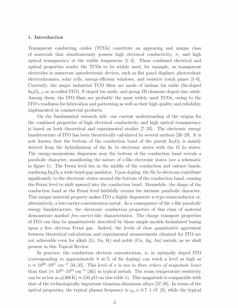
bandstructure of ITO has been theoretically calculated by several authors [26–29]. It is
now known that the bottom of the conduction band of the parent In2O3 is mainly
derived from the hybridization of the In 5s electronic states with the O 2s states.
The energy-momentum dispersion near the bottom of the conduction band reveals a
parabolic character, manifesting the nature of s-like electronic states (see a schematic
in figure 1). The Fermi level lies in the middle of the conduction and valence bands,
rendering In2O3 a wide-band-gap insulator. Upon doping, the Sn 5s electrons contribute
significantly to the electronic states around the bottom of the conduction band, causing
the Fermi level to shift upward into the conduction band. Meanwhile, the shape of the
conduction band at the Fermi level faithfully retains the intrinsic parabolic character.
This unique material property makes ITO a highly degenerate n-type semiconductor or,
alternatively, a low-carrier-concentration metal. As a consequence of the s-like parabolic
energy bandstructure, the electronic conduction properties of this class of material
demonstrate marked free-carrier-like characteristics. The charge transport properties
of ITO can thus be quantitatively described by those simple models formulated basing
upon a free electron Fermi gas. Indeed, the levels of close quantitative agreement
between theoretical calculations and experimental measurements obtained for ITO are
not achievable even for alkali (Li, Na, K) and noble (Cu, Ag, Au) metals, as we shall
present in this Topical Review.
In practice, the conduction electron concentration, n, in optimally doped ITO
(corresponding to approximately 8 at.% of Sn doping) can reach a level as high as
n ≈ 1020–1021 cm−3 [34, 35]. This level of n is two to three orders of magnitude lower
than that (≈ 1022–1023 cm−3 [36]) in typical metals. The room temperature resistivity
can be as low as ρ(300K) ≈ 150 µΩ cm (see table 1). This magnitude is comparable with
that of the technologically important titanium-aluminum alloys [37,38]. In terms of the
optical properties, the typical plasma frequency is ωp ≃ 0.7–1 eV [8], while the typical
3

Figure 1. Schematic energy bandstructure showing the top of the valence band
and the bottom of the conduction band for (a) In2O3 and (b) Sn-doped In2O3
(In2−xSnxO3−δ). This figure was reproduced with permission from [7]. Copyright
1984 by the American Physical Society.
energy band gap isEg ≃ 3.7–4.0 eV. Hence, optimally doped ITO possesses a high optical
transparency which exceeds 90% transmittance at the visible light frequencies [39,40]. A
value of ωp ≃ 1 eV corresponds to a radiation frequency of fp = ωp/2π ≃ 2.4× 10¹⁴ Hz,
which is approximately one fifth of the visible light frequency and roughly one fiftieth of
the plasma frequency of a typical metal. For optoelectronic applications, on one hand,
one would like to dope ITO with a Sn level as high as technologically feasible in order
to obtain a high electrical conductivity σ. On the other hand, since ωp ∝√n, one has
to keep n sufficiently low such that the visible light can propagate through the ITO
structure.
Owing to their technological importance, it is natural that there already exist in the
literature a number of review articles on the ITO as well as TCO materials [2,4,41–51].
The early studies up to 1982, covering the deposition methods, crystal structures,
scattering mechanisms of conduction electrons, and the optical properties of In2O3,
SnO2 and ITO, were reviewed by Jarzebski [2]. Hamberg and Granqvist discussed the
optical properties of ITO films fabricated by the reactive electron-gun evaporation onto
heated glass substrates [42]. The development up to 2000 on the various aspects of
utilizing TCOs was summarized in reports considering, for example, characterizations
[48], applications and processing [43], criteria for choosing transparent conductors [47],
new n- and p-type TCOs [44, 45], and the chemical and thin-film strategies for new
TCOs [46]. The recent progresses in new TCO materials and TCOs based devices were
discussed in [49] and [50]. King and Veal recently surveyed the current theoretical
understanding of the effects of defects, impurities, and surface states on the electrical
conduction in TCOs [51].
In this Topical Review, we stress the free-electron-like energy bandstructure and
the low-n features (as compared with typical metals) of the ITO material. These
inherited intrinsic electronic characteristics make ITO a model system which is ideal
for not only revealing the semi-classical Boltzmann transport behaviors (section 2) but
4
also studying new physics such as the quantum-interference weak-localization (WL)
effect and the universal conduction fluctuations (UCFs) in miniature structures (section
3). The responsible electron dephasing (electron-electron scattering, electron-phonon
scattering, and spin-orbit scattering) processes are discussed. Furthermore, we show
that this class of material provides a very useful platform for experimentally testing the
recent theories of granular metals [52–57]. In the last case, ultrathin ITO films can be
intentionally made to be slightly inhomogeneous or granular, while the coupling between
neighboring grains remains sufficiently strong so that the system retains global metallic-
like conduction (section 4). To illustrate the unique and numerous avenues provided
by ITO for the studies of the aforementioned semi-classical versus quantum electron
transport, as well as homogeneous versus inhomogeneous charge transport, we cover
polycrystalline (ultra)thin and thick ITO films and single-crystalline ITO nanowires in
this Topical Review. We demonstrate that high-quality ITO structures can indeed be
readily fabricated into various forms which, apart from being powerful for addressing
fundamental electronic conduction properties, may be useful for potential technological
applications. Furthermore, owing to the similarities in electronic bandstructure between
ITO and other TCO materials [3], we expect that the electronic processes and
mechanisms discussed in this Topic Review should be useful for understanding and
interpreting the results obtained on general TCOs.
We do not cover insulating or amorphous ITO materials in this Topical Review,
where the electronic conduction processes can be due to thermally excited hopping
[58–62]. In addition to the conventional Mott [63] and Efros-Shklovskii [64]
hopping conduction mechanisms in homogeneous strongly disordered systems, electronic
conduction due to the thermal charging effect [65] and, more recently, the variable-
range-hopping process [66] in inhomogeneous (granular) systems have been discussed in
literature. On the other hand, the possible occurrence of superconductivity in ITO has
been explored in references [67–70].
2. Free-electron-like Boltzmann transport: Homogeneous indium tin oxide
films and nanowires
The electrical-transport properties of ITO films have extensively been discussed in the
literature. However, previous studies have mainly concentrated on the influences of
deposition methods and conditions on the ρ(300K) values. While those studies have
provided useful information for improving the fabrication of high-quality ITO films,
they did not deal with the underlying electronic conduction processes in ITO. In
subsection 2.1, we first briefly summarize the theoretical calculations of the electronic
energy bandstructure of ITO and explain why this class of material behaves like a
highly degenerate semiconductor or a low-n metal. In subsection 2.2, we discuss the
overall temperature behavior of resistivity ρ(T ) in ITO and show that ρ(T ) can be well
described by the standard Boltzmann transport equation in a wide temperature range.
In subsection 2.3, we demonstrate that the thermoelectric power (Seebeck coefficient, or
5
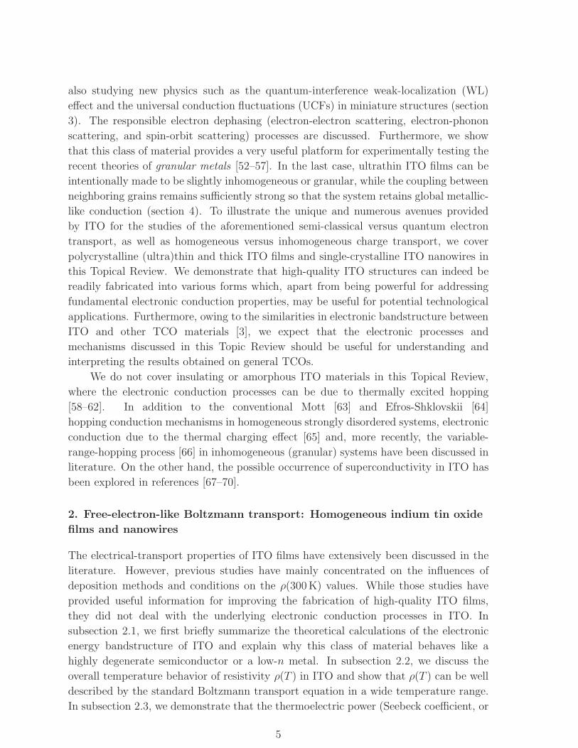
Figure 2. Electronic energy bandstructure of (a) undoped In2O3 and (b) 6.25 at.%
Sn-doped In2O3. In (b), a 6.25 at.% doping level corresponds to a single Sn atom
substituting for one of the 16 In atoms in the In2O3 supercell. Note the inherent
free-electron-like energy-momentum dispersion at the Fermi level. This figure was
reproduced with permission from [29]. Copyright 2010 by the American Physical
Society.
thermopower), S(T ), in ITO follows an approximately linear temperature dependence
in the wide temperature range from 1 K up to well above room temperature. This
linear thermoelectric power originates from the diffusion of electrons in the presence
of a temperature gradient and provides a powerful, direct manifestation of the robust
free-carrier-like characteristic of ITO. The reason why the phonon-drag contribution to
thermoelectric power in ITO is absent is heuristically discussed.
2.1. Free-carrier-like bandstructure and relevant electronic parameters
2.1.1. Electronic energy bandstructure Since the electronic energy bandstructure plays
a key role in governing the charge transport properties of a given material, we first discuss
the electronic bandstructure of ITO. Based on their x-ray photoemission spectroscopy
studies, Fan and Goodenough [71] first suggested a schematic energy band model for
the undoped and Sn-doped In2O3 in 1977. A heuristic energy-band model for ITO was
proposed by Hamberg et al [7] in 1984. In their heuristic model (shown in figure 1),
the bottom (top) of the conduction (valence) band of In2O3 was taken to be parabolic.
They further proposed that the shapes of the conduction band and the valence band
remained unchanged upon Sn doping. This simple bandstructure model is qualitatively
in line with that obtained by later theoretical calculations [26–29].
The first ab initio bandstructure calculations for the ITO material were carried out
by Odaka et al [26], and Mryasov and Freeman [27] in 2001. Later on, Medvedeva [28]
calculated the bandstructure of In2O3, and Medvedeva and Hettiarachchi [29] calculated
the bandstructure of 6.25 at.% Sn-doped In2O3. Figures 2(a) and 2(b), respectively,
6

show the electronic bandstructures of stoichiometric In2O3 and 6.25 at.% Sn-doped
In2O3 obtained in [29]. For In2O3, the conduction band exhibits a free-electron-like,
parabolic characteristic around the Γ point, where the bottom of the conduction band
originates from the hybridization of In 5s and O 2s electronic states. Medvedeva
and Hettiarachchi found that the effective electron mass, m∗, near the Γ point is
nearly isotropic. Similar theoretical results were shortly after obtained by Fuchs and
Bechstedt [72], and Karazhanov et al [12].
Upon Sn doping, the Sn 5s states further hybridize with the In 5s and O 2s states
to form the bottom of the conduction band. Furthermore, the Fermi level in ITO shifts
upward into the conduction band, leading to the bandstructure depicted in figure 2(b).
Theoretical calculations indicate that the Sn 5s states contribute nearly one fourth of
the total electronic density of states at the Fermi level, N(EF ), while the In 5s and
O 2s states contribute the rest. At this particular doping level, the s-like symmetry
of the original bandstructure around the Fermi level in the parent In2O3 is essentially
unaltered. Thus, the conduction electrons at the Fermi level in ITO possess strong
free-carrier-like features. Meanwhile, Fuchs and Bechstedt [72] found that the average
effective electron mass increases slightly with increasing carrier concentration n. At a
level of n ≃ 1020 cm−3, they obtained a value m∗ ≃ 0.3me, where me is the free-electron
mass. Their result agreed with that derived from optical measurements of the Drude
term to free carriers [7].
In brief, the combined electronic bandstructure characteristics of a wide energy gap,
a small m∗, and in particular a low n as well as a free-carrier-like dispersion at EF , are
the crucial ingredients to make ITO, on one hand, possess high electrical conductivity
while, on the other hand, reveal high optical transparency.
Figure 3. Carrier concentration as a function of temperature for as-prepared (before
annealing) and annealed ITO films. O2-HIP denotes annealing in an O2 atmosphere,
and O3 denotes annealing in an O3 atmosphere. This figure was reproduced with
permission from [73]. Copyright 2000 by the Elsevier B. V.
7

2.1.2. Relevant electronic parameters Experimentally, a reliable method to check
the metal-like energy bandstructure of a material is to examine the temperature T
dependence of n. For a metal or a highly degenerate semiconductor, n does not vary
with T . Figure 3 shows the variation of n with temperature for a few as-deposited
(before annealing) and annealed ITO films studied by Kikuchi et al [73]. It is clear
that n remains constant in a wide T range from liquid-helium temperatures up to 300
K. In the as-deposited sample, the n value approaches ∼ 1 × 1021 cm−3. Temperature
independent n in the ITO material has been reported by a number of groups [61,74–76].
For the convenience of the discussion of charge transport properties in ITO in this
Topical Review, we would like to estimate the values of relevant electronic parameters.
Consider a high-quality ITO sample having a value of ρ(300K) ≃ 150 µΩ cm, a carrier
concentration n ≃ 1×1021 cm−3, and an effective mass m∗ ≃ 0.35me. Applying the free-
electron model, we obtain the Fermi wavenumber kF = (3π2n)1/3 ≃ 3.1 × 10⁹ m−1, the
Fermi velocity vF = ~kF/m∗ ≃ 1.0×10⁶ m/s, and the Fermi energy EF = ~
2k2F/(2m
∗) ≃1.0 eV. The electron mean free time is τ = m∗/(ne2ρ) ≃ 8.3 × 10⁻¹⁵ s, corresponding
to the electron mean free path l = vF τ ≃ 8.3 nm. The electron diffusion constant
D = vF l/3 ≃ 28 cm2/s. Thus, the dimensionless product kF l ≃ 26. Note that
kF l is an important physical quantity which characterizes the degree of disorder in
a conductor. A kF l value of order a few tens indicates that high-quality ITO is a weakly
disordered metal, and should thus be rich in a variety of quantum-interference transport
phenomena.
In practice, the ρ and n values in ITO films can vary widely with the deposition
methods and conditions, Sn doping levels, and the post thermal treatment conditions. In
table 1, we list some representative values for ITO films prepared by different techniques.
This table indicates that those ITO films fabricated by the DC magnetron sputtering
method possess relatively high (low) n (ρ) values. Since the films thus prepared
are compact and they adhere well to the substrate surface, this low-cost technique
is thus the most widely used ITO deposition method in the industrial production
nowadays. Recently, researchers have also carried out molecular-beam-epitaxial growth
studies of ITO structures [94, 95], but the crystal quality obtained was not as high
as that previously achieved in the epitaxial films grown by a pulsed-laser deposition
technique [96]. We mention in passing that, apart from the bulk properties [97,98], the
effect on electronic processes of the surface states due to oxygen vacancies in undoped
In2O3−δ [32] as well as doped TCOs [30, 31, 51] has recently drawn theoretical and
experimental attention.
2.2. Temperature behavior of electrical resistivity
The temperature dependence of resistivity ρ(T ) from 300 K down to liquid-helium
temperatures provides key information for the understanding of the electrical conduction
processes in a conductor. Li and Lin [99] have measured ρ(T ) between 0.4 and 300 K in
a number of 125 and 240 nm thick polycrystalline ITO films prepared by the standard
8
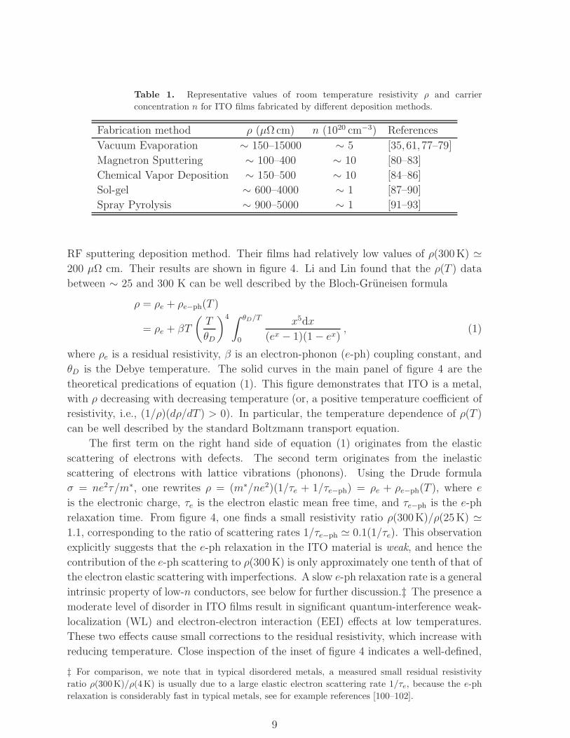
Table 1. Representative values of room temperature resistivity ρ and carrier
concentration n for ITO films fabricated by different deposition methods.
Fabrication method ρ (µΩcm) n (1020 cm−3) References
Vacuum Evaporation ∼ 150–15000 ∼ 5 [35, 61, 77–79]
Magnetron Sputtering ∼ 100–400 ∼ 10 [80–83]
Chemical Vapor Deposition ∼ 150–500 ∼ 10 [84–86]
Sol-gel ∼ 600–4000 ∼ 1 [87–90]
Spray Pyrolysis ∼ 900–5000 ∼ 1 [91–93]
RF sputtering deposition method. Their films had relatively low values of ρ(300K) ≃200 µΩ cm. Their results are shown in figure 4. Li and Lin found that the ρ(T ) data
between ∼ 25 and 300 K can be well described by the Bloch-Gruneisen formula
ρ = ρe + ρe−ph(T )
= ρe + βT
(
T
θD
)4 ∫ θD/T
0
x5dx
(ex − 1)(1− ex), (1)
where ρe is a residual resistivity, β is an electron-phonon (e-ph) coupling constant, and
θD is the Debye temperature. The solid curves in the main panel of figure 4 are the
theoretical predications of equation (1). This figure demonstrates that ITO is a metal,
with ρ decreasing with decreasing temperature (or, a positive temperature coefficient of
resistivity, i.e., (1/ρ)(dρ/dT ) > 0). In particular, the temperature dependence of ρ(T )
can be well described by the standard Boltzmann transport equation.
The first term on the right hand side of equation (1) originates from the elastic
scattering of electrons with defects. The second term originates from the inelastic
scattering of electrons with lattice vibrations (phonons). Using the Drude formula
σ = ne2τ/m∗, one rewrites ρ = (m∗/ne2)(1/τe + 1/τe−ph) = ρe + ρe−ph(T ), where e
is the electronic charge, τe is the electron elastic mean free time, and τe−ph is the e-ph
relaxation time. From figure 4, one finds a small resistivity ratio ρ(300K)/ρ(25K) ≃1.1, corresponding to the ratio of scattering rates 1/τe−ph ≃ 0.1(1/τe). This observation
explicitly suggests that the e-ph relaxation in the ITO material is weak, and hence the
contribution of the e-ph scattering to ρ(300K) is only approximately one tenth of that of
the electron elastic scattering with imperfections. A slow e-ph relaxation rate is a general
intrinsic property of low-n conductors, see below for further discussion.‡ The presence a
moderate level of disorder in ITO films result in significant quantum-interference weak-
localization (WL) and electron-electron interaction (EEI) effects at low temperatures.
These two effects cause small corrections to the residual resistivity, which increase with
reducing temperature. Close inspection of the inset of figure 4 indicates a well-defined,
‡ For comparison, we note that in typical disordered metals, a measured small residual resistivity
ratio ρ(300K)/ρ(4K) is usually due to a large elastic electron scattering rate 1/τe, because the e-ph
relaxation is considerably fast in typical metals, see for example references [100–102].
9

Figure 4. Normalized resistivity, ρ(T )/ρ(300K), as a function of temperature for
a 125 nm (squares) and a 240 nm (triangles) thick ITO films. The symbols are the
experimental data and the solid curves are the theoretical predictions of equation (1).
For clarity, the data for the 240 nm thick film has been shifted up by 0.01. Inset:
Normalized sheet resistance, ∆R(T )/R = [R(T ) − R(20.5K)]/R(20.5K), as a
function of the logarithm of temperature for these two films below 25 K. The straight
solid lines are least-squares fits to the theoretical predictions of 2D WL and EEI effects.
This figure was reproduced with permission from [99]. Copyright 2004 by the American
Institute of Physics.
logarithmic temperature dependent resistivity rise below ∼ 25 K. The two-dimensional
(2D) WL and EEI effects will be discussed in section 3.
In addition to comparatively thick films, present-day RF sputtering deposition
technology has advanced such that relatively thin films can be made metallic. In a
recent study, Lin et al [103] found that the temperature dependence of ρ(T ) below
300 K for 15 nm thick polycrystalline ITO films can also be described by the Bloch-
Gruneisen formula. However, the ρ(T ) curve reaches a minimum around 150 K. At
lower temperatures, ρ(T ) increases with decreasing temperature, signifying much more
pronounced 2D WL and EEI effects than in thicker films (figure 4).
The temperature dependence of resistivity in single-crystalline ITO nanowire has
been investigated by Chiu et al [69]. They measured individual ITO nanowires from
300 K down to 1.5 K employing an electron-beam lithographic four-probe configuration.
Figure 5 shows a plot of the normalized resistivity, ρ(T )/ρ(300K), as a function of
temperature for four ITO nanowires. The solid curves are the theoretical predications
of equation (1), indicating that the experimental ρ(T ) data can be well described by the
Bloch-Gruneisen formula. However, it is surprising that, in the wide temperature range
1–300 K, the resistivity drops by no more than ∼ 20%, even though these nanowires are
single-crystalline. This observation strongly suggests that these nanowires must contain
high levels of point defects which are not detectable by the high-resolution transmission
electron microscopy studies [69]. It is worth noting that these nanowires are three-
10
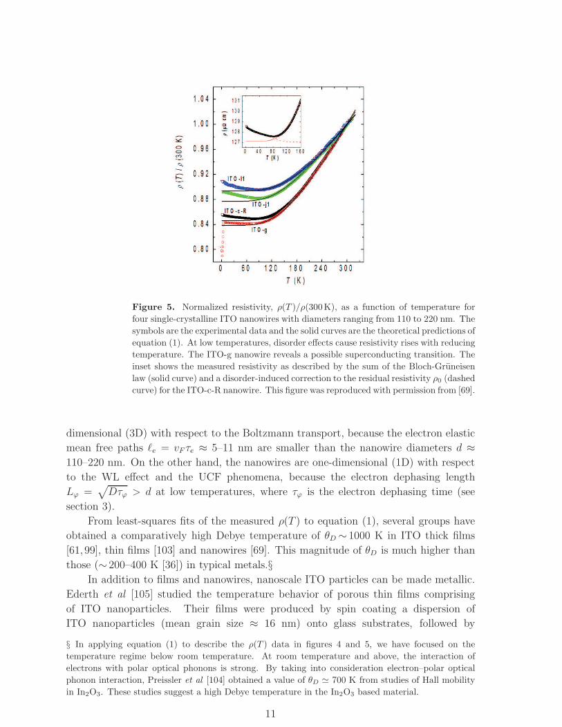
Figure 5. Normalized resistivity, ρ(T )/ρ(300K), as a function of temperature for
four single-crystalline ITO nanowires with diameters ranging from 110 to 220 nm. The
symbols are the experimental data and the solid curves are the theoretical predictions of
equation (1). At low temperatures, disorder effects cause resistivity rises with reducing
temperature. The ITO-g nanowire reveals a possible superconducting transition. The
inset shows the measured resistivity as described by the sum of the Bloch-Gruneisen
law (solid curve) and a disorder-induced correction to the residual resistivity ρ0 (dashed
curve) for the ITO-c-R nanowire. This figure was reproduced with permission from [69].
dimensional (3D) with respect to the Boltzmann transport, because the electron elastic
mean free paths ℓe = vF τe ≈ 5–11 nm are smaller than the nanowire diameters d ≈110–220 nm. On the other hand, the nanowires are one-dimensional (1D) with respect
to the WL effect and the UCF phenomena, because the electron dephasing length
Lϕ =√
Dτϕ > d at low temperatures, where τϕ is the electron dephasing time (see
section 3).
From least-squares fits of the measured ρ(T ) to equation (1), several groups have
obtained a comparatively high Debye temperature of θD ∼ 1000 K in ITO thick films
[61, 99], thin films [103] and nanowires [69]. This magnitude of θD is much higher than
those (∼ 200–400 K [36]) in typical metals.§In addition to films and nanowires, nanoscale ITO particles can be made metallic.
Ederth et al [105] studied the temperature behavior of porous thin films comprising
of ITO nanoparticles. Their films were produced by spin coating a dispersion of
ITO nanoparticles (mean grain size ≈ 16 nm) onto glass substrates, followed by
§ In applying equation (1) to describe the ρ(T ) data in figures 4 and 5, we have focused on the
temperature regime below room temperature. At room temperature and above, the interaction of
electrons with polar optical phonons is strong. By taking into consideration electron–polar optical
phonon interaction, Preissler et al [104] obtained a value of θD ≃ 700 K from studies of Hall mobility
in In2O3. These studies suggest a high Debye temperature in the In2O3 based material.
11
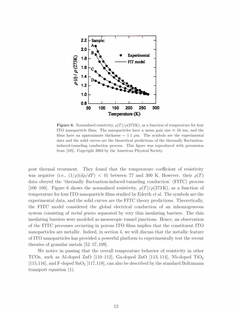
Figure 6. Normalized resistivity, ρ(T )/ρ(273K), as a function of temperature for four
ITO nanoparticle films. The nanoparticles have a mean gain size ≈ 16 nm, and the
films have an approximate thickness ∼ 1.1 µm. The symbols are the experimental
data and the solid curves are the theoretical predictions of the thermally fluctuation-
induced-tunneling conduction process. This figure was reproduced with permission
from [105]. Copyright 2003 by the American Physical Society.
post thermal treatment. They found that the temperature coefficient of resistivity
was negative (i.e., (1/ρ)(dρ/dT ) < 0) between 77 and 300 K. However, their ρ(T )
data obeyed the ‘thermally fluctuation-induced-tunneling conduction’ (FITC) process
[106–108]. Figure 6 shows the normalized resistivity, ρ(T )/ρ(273K), as a function of
temperature for four ITO nanoparticle films studied by Ederth et al. The symbols are the
experimental data, and the solid curves are the FITC theory predictions. Theoretically,
the FITC model considered the global electrical conduction of an inhomogeneous
system consisting of metal grains separated by very thin insulating barriers. The thin
insulating barriers were modeled as mesoscopic tunnel junctions. Hence, an observation
of the FITC processes occurring in porous ITO films implies that the constituent ITO
nanoparticles are metallic. Indeed, in section 4, we will discuss that the metallic feature
of ITO nanoparticles has provided a powerful platform to experimentally test the recent
theories of granular metals [52–57, 109].
We notice in passing that the overall temperature behavior of resistivity in other
TCOs, such as Al-doped ZnO [110–112], Ga-doped ZnO [113, 114], Nb-doped TiO2
[115,116], and F-doped SnO2 [117,118], can also be described by the standard Boltzmann
transport equation (1).
12

2.3. Linear temperature dependence of thermoelectric power
The thermoelectric power is an important physical quantity which describes the
electronic conduction behaviors in the presence of a temperature gradient and under
the open circuit situation. Studies of the temperature dependence of thermopower,
S(T ), can provide useful information about the electronic density of states at the Fermi
level N(EF ), the magnitude of EF , the responsible carrier types (electrons and/or holes),
as well as the phonon-electron and phonon-phonon relaxation processes in the material.
In a metal, the thermopower arises from two contributions and can be expressed as
S(T ) = Sd(T ) + Sg(T ), where Sd(T ) is the electron-diffusion contribution, and Sg(T ) is
the phonon-drag contribution [119, 120].
2.3.1. Electron-diffusion thermopower The electron diffusion contribution stems from
the diffusion of thermal electrons in the presence of a temperature gradient. A general
form is given by the Mott formula [119]
Sd(T ) = −π2k2BT
3|e|EF
d lnσ(E)
d lnE
∣
∣
∣
E=EF
, (2)
where kB is the Boltzmann constant, and σ(E) is the conductivity of electrons that
have energy E. The Mott formula is derived under the assumption that the phonon
distribution is itself in overall equilibrium at temperature T . Note that in the case of
hole conduction the minus sign in equation (4) should be replaced by a plus sign.
Consider a free electron Fermi gas. By substituting the Einstein relation σ(E) =
N(E)e2D(E) into equation (2), where D(E) = v2(E)τ(E)/3 is the electron diffusion
constant in a 3D conductor with respect to the Boltzmann transport, and v(E) is the
electron velocity, one obtains
Sd(T ) = −π2k2BT
3|e|EF
[3
2+
d ln τ(E)
d lnE
]∣
∣
∣
E=EF
. (3)
Equation (3) predicts a linear temperature dependence of Sd. The slope of this linear
T dependence varies inversely with EF , and its precise value is governed by the energy
dependence of mean-free time τ(E) ∝ Eq, where q is an exponent of order unity.
The temperature behavior of Sd in the low temperature limit (which is pertinent to
ITO) can be approximated as follows. At T ≪ θD and in the presence of notable defect
scattering such that the electron mean free path l(E) = v(E)τ(E) is nearly a constant,
i.e., τ(E) ∝ 1/v(E) ∝ 1/√E, equation (3) reduces to
Sd = −π2k2BT
3|e|EF. (4)
Since the typical EF value in ITO is one order of magnitude smaller than that in a typical
metal, the Sd value in the former is thus approximately one order of magnitude larger
than that in the latter. Alternatively, equation (4) can be rewritten in the following
form: Sd = −2Ce/(3n|e|), where Ce = π2nk2BT/(2EF ) is the electronic specific heat per
unit volume. This expression will be used in equation (5).
13
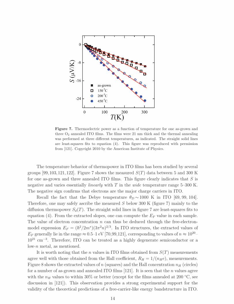
Figure 7. Thermoelectric power as a function of temperature for one as-grown and
three O2 annealed ITO films. The films were 21 nm thick and the thermal annealing
was performed at three different temperatures, as indicated. The straight solid lines
are least-squares fits to equation (4). This figure was reproduced with permission
from [121]. Copyright 2010 by the American Institute of Physics.
The temperature behavior of thermopower in ITO films has been studied by several
groups [99,103,121,122]. Figure 7 shows the measured S(T ) data between 5 and 300 K
for one as-grown and three annealed ITO films. This figure clearly indicates that S is
negative and varies essentially linearly with T in the wide temperature range 5–300 K.
The negative sign confirms that electrons are the major charge carriers in ITO.
Recall the fact that the Debye temperature θD ∼ 1000 K in ITO [69, 99, 104].
Therefore, one may safely ascribe the measured S below 300 K (figure 7) mainly to the
diffusion thermopower Sd(T ). The straight solid lines in figure 7 are least-squares fits to
equation (4). From the extracted slopes, one can compute the EF value in each sample.
The value of electron concentration n can thus be deduced through the free-electron-
model expression EF = (~2/2m∗)(3π2n)2/3. In ITO structures, the extracted values of
EF generally lie in the range≈ 0.5–1 eV [70,99,121], corresponding to values of n ≈ 1020–
1021 cm−3. Therefore, ITO can be treated as a highly degenerate semiconductor or a
low-n metal, as mentioned.
It is worth noting that the n values in ITO films obtained from S(T ) measurements
agree well with those obtained from the Hall coefficient, RH = 1/(nHe), measurements.
Figure 8 shows the extracted values of n (squares) and the Hall concentration nH (circles)
for a number of as-grown and annealed ITO films [121]. It is seen that the n values agree
with the nH values to within 30% or better (except for the films annealed at 200 C, see
discussion in [121]). This observation provides a strong experimental support for the
validity of the theoretical predictions of a free-carrier-like energy bandstructure in ITO.
14

Figure 8. Variation in carrier concentration and Fermi energy with annealing
temperature for a good number of 21 nm thick ITO films. Open (closed) squares:
n for air (oxygen) annealed films; open (closed) circles: nH for air (oxygen) annealed
films. This figure was reproduced with permission from [121]. Copyright 2010 by the
American Institute of Physics.
In fact, such kind of prevailing linearity in S(T ) from liquid-helium temperatures all the
way up to at least 300 K (figure 7) is seldom seen in any textbook simple metals, where
the phonon-drag contribution Sg(T ) often causes profound, non-monotonic temperature
behavior of S(T ) (see, for example, reference [120] and the figures 7.10 and 7.12 in
reference [123]). Thus, ITO does serve as a model system for studying electronic
conduction phenomena and extracting reliable electronic parameters.
2.3.2. Phonon-drag thermopower We would like to comment on the negligible phonon-
drag contribution to the measured S(T ) in the ITO material. The phonon-drag term
stems from the interaction between heat conducting phonons with conduction electrons.
In ITO (figures 7), the prevailing linearity over a wide range of temperature is a direct
and strong indication of the absence of the phonon-drag contribution. The reason for the
practically complete suppression of the phonon-drag term can be explained as follows.
Considering the phonon scattering processes and ignoring their frequency dependence,
the phonon-drag thermopower Sg(T ) at T <θD can be approximated by [119, 123]
Sg ≃ − Cg
3n|e|
(
τphτph + τph−e
)
≃ − Cg
3n|e|
(
τphτph−e
)
≃ 1
2
(
τphτe−ph
)
Sd , (5)
where Cg is the lattice specific heat per unit volume, τph is the phonon relaxation
time due to all kinds of phonon scattering processes (such as phonon-phonon (ph-ph)
15

scattering, phonon scattering with imperfections, etc.) except the phonon-electron (ph-
e) scattering, and τph−e is the ph-e scattering time. In writing equation (5), we have
assumed that τph ≪ τph−e. Note that we have also applied the the energy-balance
equation Ce/τe−ph = Cg/τph−e (references [124, 125]) to replace τph−e by τe−ph.
Consider a representative temperature of 100 K∼ 0.1θD in ITO. We take the phonon
mean free path to be few nanometers long [126–128], which corresponds to a relaxation
time τph(100K)∼ 10−12 s, with a sound velocity vp ≃ 4400 m/s in ITO [126]. According
to our previous studies of the weak-localization effect in ITO films [129], we estimate
τe−ph(100K)∼ 10−11 s. Thus, equation (5) indicates that the phonon-drag term would
contribute only a few percent to the measured thermopower at a temperature of 100
K. The underlying physics for the smallness of the phonon-drag term Sg can further
be reasoned as follows. (i) The value of τph in ITO is generally very short due to the
presence of a moderately high level of disorder in this class of material. (ii) Since
the e-ph coupling strength in a conductor is proportional to the carrier concentration
n [101,129], the relaxation time τe−ph in ITO is thus notably long compared with that in
typical metals. (See further discussion in subsection 3.1.2.) These two intrinsic material
characteristics combine to cause a small τph/τe−ph ratio, and hence Sg ≪ Sd in the ITO
material. By the same token, a linear temperature dependence of S(T ) with negligible
contribution from Sg has recently been observed in F-doped SnO2 films [118].
3. Quantum-interference transport at low temperature: Homogeneous
indium tin oxide films and nanowires
In section 2, we have examined the temperature dependence of electrical resistivity and
thermoelectric power over a wide temperature range to demonstrate that the electronic
conduction properties of metallic ITO obey the standard Boltzmann transport equation.
In particular, being inherited with a free-carrier-like energy bandstructure, the essential
electronic parameters can be reliably extracted from combined ρ(T ), S(T ) and Hall
coefficient RH measurements. In this section, we show that metallic ITO also opens
avenues for the studies of quantum electron transport properties. We shall focus on
the quantum-interference weak-localization (WL) effect and the universal conductance
fluctuation (UCF) phenomenon, which manifest in ITO films and nanowires at low
temperatures. The many-body electron-electron interaction (EEI) effect in homogeneous
disordered systems will not be explicitly discussed in this Topical Review, but will be
briefly mentioned where appropriate.
3.1. Weak-localization effect and electron dephasing time
The WL effect and electron dephasing in disordered conductors have been studied
for three decades [130–135]. During this time, the mesoscopic and nanoscale physics
underlying these processes has witnessed significant theoretical and experimental
advances. Over years, the WL effect has also been explored in a few TCO materials,
16
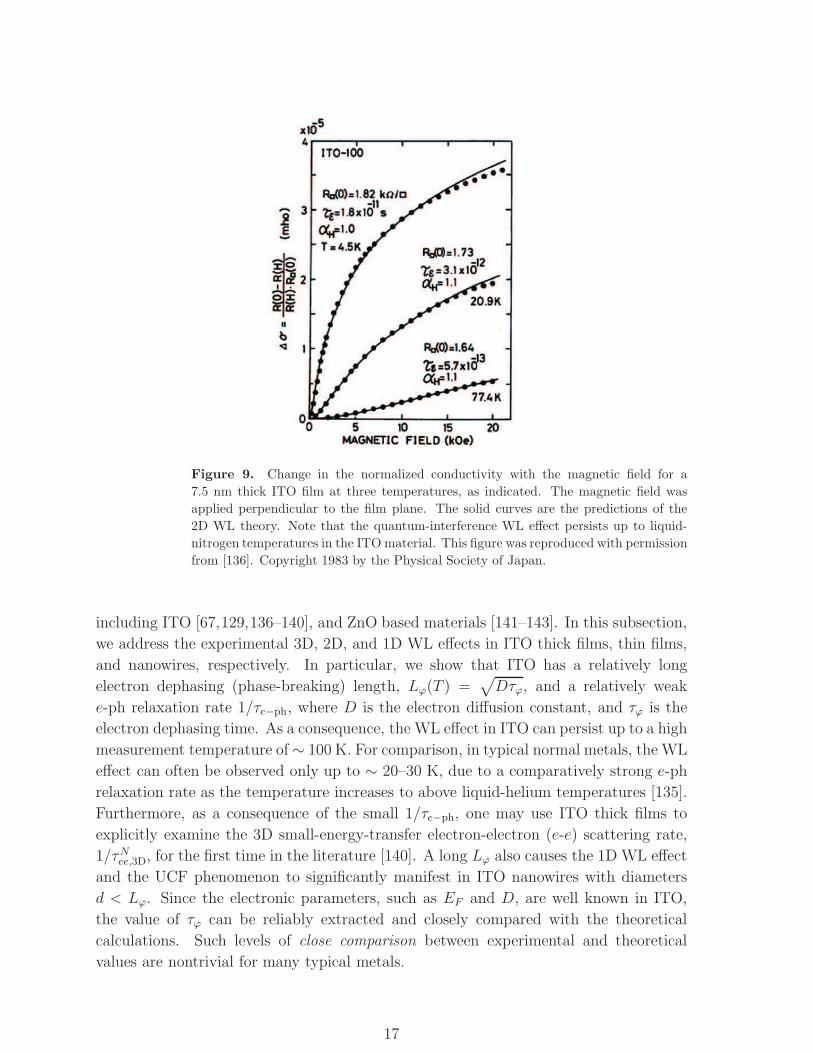
Figure 9. Change in the normalized conductivity with the magnetic field for a
7.5 nm thick ITO film at three temperatures, as indicated. The magnetic field was
applied perpendicular to the film plane. The solid curves are the predictions of the
2D WL theory. Note that the quantum-interference WL effect persists up to liquid-
nitrogen temperatures in the ITOmaterial. This figure was reproduced with permission
from [136]. Copyright 1983 by the Physical Society of Japan.
including ITO [67,129,136–140], and ZnO based materials [141–143]. In this subsection,
we address the experimental 3D, 2D, and 1D WL effects in ITO thick films, thin films,
and nanowires, respectively. In particular, we show that ITO has a relatively long
electron dephasing (phase-breaking) length, Lϕ(T ) =√
Dτϕ, and a relatively weak
e-ph relaxation rate 1/τe−ph, where D is the electron diffusion constant, and τϕ is the
electron dephasing time. As a consequence, the WL effect in ITO can persist up to a high
measurement temperature of∼ 100 K. For comparison, in typical normal metals, the WL
effect can often be observed only up to ∼ 20–30 K, due to a comparatively strong e-ph
relaxation rate as the temperature increases to above liquid-helium temperatures [135].
Furthermore, as a consequence of the small 1/τe−ph, one may use ITO thick films to
explicitly examine the 3D small-energy-transfer electron-electron (e-e) scattering rate,
1/τNee,3D, for the first time in the literature [140]. A long Lϕ also causes the 1D WL effect
and the UCF phenomenon to significantly manifest in ITO nanowires with diameters
d < Lϕ. Since the electronic parameters, such as EF and D, are well known in ITO,
the value of τϕ can be reliably extracted and closely compared with the theoretical
calculations. Such levels of close comparison between experimental and theoretical
values are nontrivial for many typical metals.
17

3.1.1. Weak-localization magnetoresistance in various dimensions As discussed in
section 2, ρ(T ) of ITO samples decrease by small amounts (. 10% in polycrystalline
films and . 20% in single-crystalline nanowires) as the temperature decreases from
300 K down to liquid-helium (or liquid-nitrogen) temperatures, suggesting the presence
of moderately high levels of disorder in all kinds of ITO materials. Thus, the WL
effect must prevail in ITO. In 1983, Ohyama et al [136] measured ITO thin films and
found negative magnetoresistance (MR) and logarithmic temperature dependence of
resistance in a wide temperature range 1.5–100 K. They explained the negative MR in
terms of the 2D WL effect and the logarithmic temperature dependence of resistance
in terms of a sum of the 2D WL and EEI effects. Figure 9 shows a plot of the positive
magnetoconductance (i.e., negative MR) induced by the WL effect in a 7.5 nm thick
ITO film measured by Ohyama and coworkers. It is seen that the experimental data
(symbols) can be well described by the 2D WL theory predictions (solid curves).
Recently, with the advances of nanoscience and technology, the 1D WL effect has
been investigated in single-crystalline ITO nanowires [137–139]. In particular, since Lϕ
is relatively long in the ITO material at low temperatures (see below), the quasi-1D
dimensional criterion Lϕ > d is readily achieved. Thus, significant 1D WL effects can
be seen in ITO nanowires. Indeed, figure 10(a) shows a plot of the negative MR due
to the 1D WL effect in a 60 nm diameter ITO nanowire studied by Hsu et al [138].
This nanowire had a low resistivity value of ρ(10K) ≃ 185 µΩ cm. The magnetic field
was applied perpendicular to the nanowire axis. The data (symbols) is well described
by the 1D WL theory predictions (solid curves). The extracted dephasing lengths are
Lϕ(0.25K) ≃ 520 nm and Lϕ(40K) ≃ 150 nm. Similarly, the negative MR in the 3D
WL effect can be observed in ITO thick films and is well described by the 3D WL theory
predictions. (The explicit theoretical predictions for the 1D, 2D, and 3D MR in the WL
effect can be found in [143] and references therein.)
3.1.2. Electron dephasing time Measurements of MR in the WL effect allows one to
extract the value of τϕ. Detailed studies of the electron dephasing processes in ITO
thin films have recently been carried out by Wu et al [129]. They have measured the
negative MR due to the 2D WL effect and extracted the τϕ values in two series of 15
and 21 nm thick ITO films in a wide temperature range 0.3–90 K. Figure 11 shows
a plot of representative variation of extracted 1/τϕ with temperature. In general, the
responsible dephasing processes are determined by the sample dimensionality, level of
disorder, and measurement temperature [133,135,144]. In 3D weakly disordered metals,
e-ph scattering is often the dominant dephasing mechanism [100, 135, 145], while in
reduced dimensions (2D and 1D), the e-e scattering is the major dephasing process
[135, 144, 146, 147]. As T → 0 K, a constant or very weakly temperature dependent
dephasing process may exist in a given sample, the physical origin for which is yet to be
fully identified [135,148–152]. In ITO, as already mentioned, the e-ph relaxation rate is
very weak.
The total electron dephasing rate 1/τϕ(T ) (the solid curves) in figure 11 for the 2D
18

Figure 10. Normalized magnetoresistance, ∆R(B)/R(0) = [R(B) − R(0)]/R(0), as
a function of magnetic field of (a) a 60 nm diameter ITO nanowire at (from bottom
up): 0.25, 5.0, 12, 20, 30, and 40 K, and (b) a 72 nm diameter ITO nanowire at (from
top down): 0.26, 1.0, 2.0, and 4.0 K. The magnetic field was applied perpendicular to
the nanowire axis. The symbols are the experimental data and the solid curves are
the 1D WL theory predictions. Note that the MRs are negative in (a) (i.e., the weak-
localization effect), while positive in (b) (i.e., the weak-antilocalization effect) in small
magnetic fields. This figure was reproduced with permission from [138]. Copyright
2010 by the American Physical Society.
ITO thin films studied by Wu et al [129] is described by
1
τϕ(T )=
1
τ 0ϕ+ AN
ee,2DT + Aee,2DT2 ln
(
EF
kBT
)
, (6)
where the first, second, and third terms on the right-hand side of the equation stand for
the “saturation” term, the small-energy-transfer (Nyquist) e-e scattering term, and the
large-energy-transfer e-e scattering term, respectively. The small-energy-transfer term is
dominant at low temperatures of T < ~/(kBτe), while the large-energy-transfer term is
dominant at high temperatures of T > ~/(kBτe). By comparing their measured 1/τϕ(T )
with equation (11), Wu et al found that their extracted values of the e-e scattering
strengths ANee,2D ≈ 3 × 10⁹ K−1 s−1 and Aee,2D ≈ 9 × 10⁶ K−2 s−1 are consistent with
the theoretical values to within a factor of ∼ 3 and ∼ 5, respectively.‖ Considering that
the ITO material is a disordered In2−xSnxO3−δ with random Sn dopants and possible
oxygen vacancies, such levels of agreement between experimental and theoretical values
are satisfactory. The good theoretical estimates must derive from the free-carrier-like
energy bandstructure characteristics of ITO, which renders evaluations of the electronic
parameters reliable. In terms of dephasing length, figure 11 gives rise to relatively long
length scales of Lϕ(0.3K) ≈ 500 nm and Lϕ(60K) ≈ 45 nm.
The e-e scattering rate in other-dimensional ITO samples has also been studied.
‖ The theoretical expressions for the small-energy-transfer and large-energy-transfer e-e scattering
strengths, respectively, are ANee,2D = (e2/2π~2)RkB ln(π~/e2R) and Aee,2D = πk2B/(2~EF ), where
R is the sheet resistance. In the comparison of experiment with theory, the R value was directly
measured, and the EF value was extracted from thermoelectric power measurement.
19
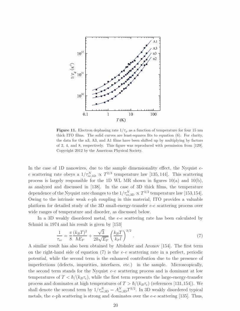
Figure 11. Electron dephasing rate 1/τϕ as a function of temperature for four 15 nm
thick ITO films. The solid curves are least-squares fits to equation (6). For clarity,
the data for the n3, A3, and A1 films have been shifted up by multiplying by factors
of 2, 4, and 8, respectively. This figure was reproduced with permission from [129].
Copyright 2012 by the American Physical Society.
In the case of 1D nanowires, due to the sample dimensionality effect, the Nyquist e-
e scattering rate obeys a 1/τNee,1D ∝ T 2/3 temperature law [135, 144]. This scattering
process is largely responsible for the 1D WL MR shown in figures 10(a) and 10(b),
as analyzed and discussed in [138]. In the case of 3D thick films, the temperature
dependence of the Nyquist rate changes to the 1/τNee,3D ∝ T 3/2 temperature law [153,154].
Owing to the intrinsic weak e-ph coupling in this material, ITO provides a valuable
platform for detailed study of the 3D small-energy-transfer e-e scattering process over
wide ranges of temperature and disorder, as discussed below.
In a 3D weakly disordered metal, the e-e scattering rate has been calculated by
Schmid in 1974 and his result is given by [153]
1
τee=
π
8
(kBT )2
~EF+
√3
2~√EF
(
kBT
kF l
)3/2
. (7)
A similar result has also been obtained by Altshuler and Aronov [154]. The first term
on the right-hand side of equation (7) is the e-e scattering rate in a perfect, periodic
potential, while the second term is the enhanced contribution due to the presence of
imperfections (defects, impurities, interfaces, etc.) in the sample. Microscopically,
the second term stands for the Nyquist e-e scattering process and is dominant at low
temperatures of T < ~/(kBτe), while the first term represents the large-energy-transfer
process and dominates at high temperatures of T > ~/(kBτe) (references [131,154]). We
shall denote the second term by 1/τNee,3D = ANee,3DT
3/2. In 3D weakly disordered typical
metals, the e-ph scattering is strong and dominates over the e-e scattering [135]. Thus,
20
equation (7) has been difficult to test in a quantitative manner for decades, even though
the mesoscopic physics has witnessed marvelous advances.
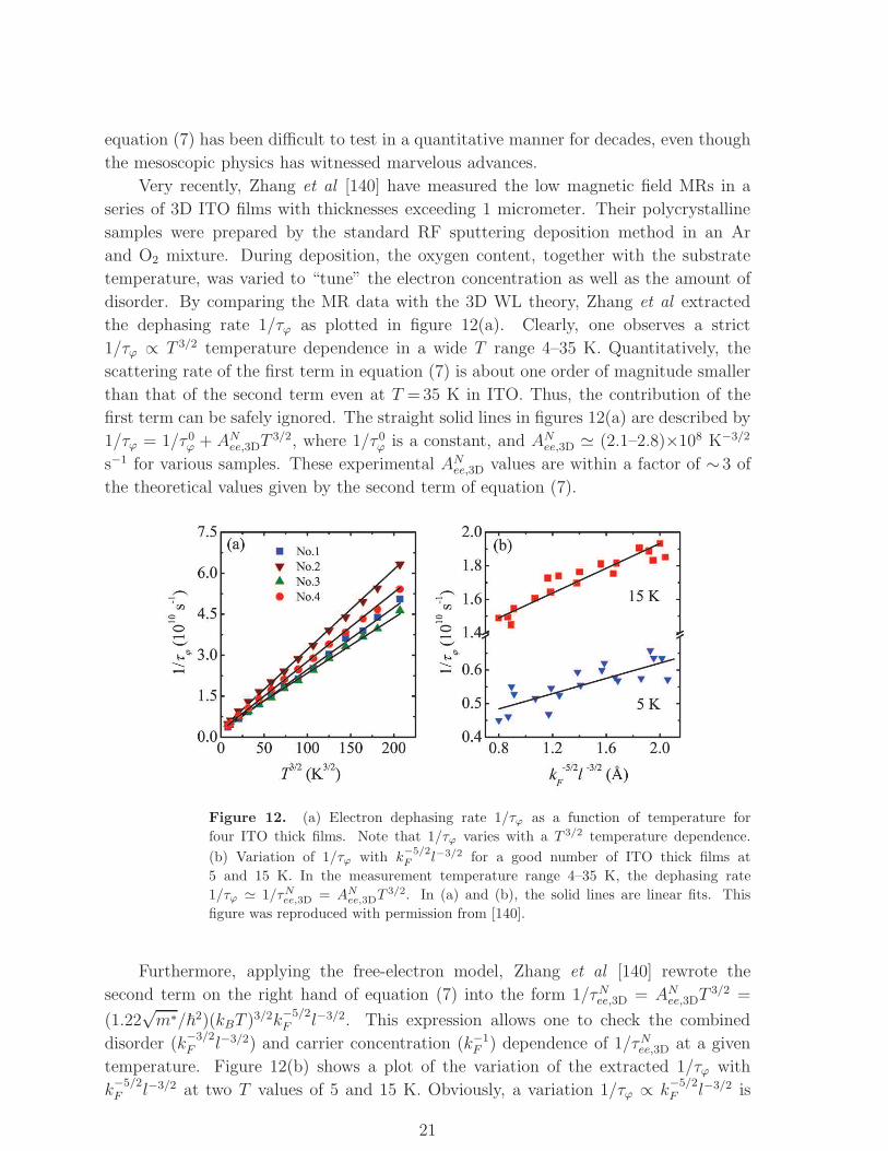
Very recently, Zhang et al [140] have measured the low magnetic field MRs in a
series of 3D ITO films with thicknesses exceeding 1 micrometer. Their polycrystalline
samples were prepared by the standard RF sputtering deposition method in an Ar
and O2 mixture. During deposition, the oxygen content, together with the substrate
temperature, was varied to “tune” the electron concentration as well as the amount of
disorder. By comparing the MR data with the 3D WL theory, Zhang et al extracted
the dephasing rate 1/τϕ as plotted in figure 12(a). Clearly, one observes a strict
1/τϕ ∝ T 3/2 temperature dependence in a wide T range 4–35 K. Quantitatively, the
scattering rate of the first term in equation (7) is about one order of magnitude smaller
than that of the second term even at T =35 K in ITO. Thus, the contribution of the
first term can be safely ignored. The straight solid lines in figures 12(a) are described by
1/τϕ = 1/τ 0ϕ + ANee,3DT
3/2, where 1/τ 0ϕ is a constant, and ANee,3D ≃ (2.1–2.8)×108 K−3/2
s−1 for various samples. These experimental ANee,3D values are within a factor of ∼ 3 of
the theoretical values given by the second term of equation (7).
Figure 12. (a) Electron dephasing rate 1/τϕ as a function of temperature for
four ITO thick films. Note that 1/τϕ varies with a T 3/2 temperature dependence.
(b) Variation of 1/τϕ with k−5/2F l−3/2 for a good number of ITO thick films at
5 and 15 K. In the measurement temperature range 4–35 K, the dephasing rate
1/τϕ ≃ 1/τNee,3D = ANee,3DT
3/2. In (a) and (b), the solid lines are linear fits. This
figure was reproduced with permission from [140].
Furthermore, applying the free-electron model, Zhang et al [140] rewrote the
second term on the right hand of equation (7) into the form 1/τNee,3D = ANee,3DT
3/2 =
(1.22√m∗/~2)(kBT )
3/2k−5/2F l−3/2. This expression allows one to check the combined
disorder (k−3/2F l−3/2) and carrier concentration (k−1
F ) dependence of 1/τNee,3D at a given
temperature. Figure 12(b) shows a plot of the variation of the extracted 1/τϕ with
k−5/2F l−3/2 at two T values of 5 and 15 K. Obviously, a variation 1/τϕ ∝ k
−5/2F l−3/2 is
21

observed. Quantitatively, the experimental slopes (≃ 1.2× 10¹⁹ and 3.7× 10¹⁹ m−1 s−1
at 5 and 15 K, respectively) in figure 12(b) are within a factor of ∼ 5 of the theoretical
values. Thus, the experimental dephasing rate 1/τϕ ≃ 1/τNee,3D = ANee,3DT
3/2 in ITO
thick films quantitatively confirms the temperature, disorder and carrier concentration
dependences of the Schmid-Altshuler-Aronov theory of 3D small-energy-transfer e-e
scattering in disordered metals [153, 154].
Electron-phonon relaxation rate. We would like to comment on the reason why the
e-e scattering dominates the electron dephasing rate in 3D ITO thick films (figure 12) in
a wide T range up to several tens of degrees of kelvin. The reason is owing to the fact that
the ITO material possesses relatively low n values which result in a greatly suppressed
1/τe−ph ≪ 1/τNee,3D. Theoretically, it is established that the electron scattering by
transverse vibrations of defects and impurities dominates the e-ph relaxation. In the
quasi-ballistic limit (qT l > 1, where qT is the wavenumber of a thermal phonon),¶ the
electron-transverse phonon scattering rate is given by [101, 145, 155]
1
τe−t,ph
=3π2k2
Bβt
(pFut)(pF l)T 2 , (8)
where βt = (2EF/3)2N(EF )/(2ρmu
2t ) is the electron-transverse phonon coupling
constant, pF is the Fermi momentum, ut is the transverse sound velocity, and ρm is the
mass density. Since the electronic parameters EF , pF , N(EF ) and l in ITO samples are
known, the theoretical value of equation (8) can be computed and is of the magnitude
1/τe−t,ph ∼ 4×10⁶ T 2 K−2 s−1. Note that this relaxation rate is about one order of
magnitude smaller than 1/τNee,3D even at a relatively high temperature of 40 K. A weak
e-ph relaxation rate allows the quantum-interference WL effect and UCF phenomena to
persist up to a few tens of degrees of kelvin in ITO.+
We reiterate that equation (8) predicts a relaxation rate 1/τe−t,ph ∝ n. On the
other hand, equation (7) predicts a scattering rate 1/τNee,3D ∝ n−5/6. Thus, the ratio of
these two scattering rates varies approximately inversely with the square of n, namely,
(1/τNee,3D)/(1/τe−t,ph) ∝ n−2. Since the n values in ITO samples are relatively low, the 3D
small-energy-transfer e-e scattering rate can thus be enhanced over the e-ph relaxation
rate. This observation can be extended to other TCO materials, and is worth of further
investigations.
We also would like to note that, in recent studies of superconducting hot electron
bolometers, a weak e-ph relaxation rate has been observed in quasi-2D heterostructures
¶ In high-quality ITO structures, qT l≈ 0.1T [129, 140], and hence the quasi-ballistic limit is valid
above ∼ 10 K. In disordered normal metals, due to a relatively short electron mean free path
l=3π2~/(e2k2F ρ)∝ 1/k2F for a same ρ value, the quasi-ballistic regime is more difficult to realize in
experiment. For example, a polycrystalline Ti73Al27 alloy [157] (an amorphous CuZrAl alloy [158])
with ρ ≈ 225 µΩ cm (≈ 200 µΩ cm) has a value of qT l ≈ 0.006T (≈ 0.01T ).+ The electron dephasing length Lϕ =
√
Dτϕ ≃√
Dτe−ph above a few degrees of kelvin is much shorter
in a typical disordered metal than in ITO, due to both a much shorter τe−ph and a smaller diffusion
constant D ∝ 1/(N(EF )ρ) ∝ 1/N(EF ) for a same ρ value in the former.
22

containing ultrathin La2−xSrxCuO4 (LSCO) layers [156]. LSCO has a n value about
two orders of magnitude lower that in the conventional superconductor NbN, and hence
τe−ph(LSCO) is nearly two orders of magnitude longer than τe−ph(NbN). In short, we
remark that slow e-ph relaxation is a general intrinsic property of low-n conductors.
Generally speaking, one may keep in mind that the relaxation rate varies approximately
as 1/τe−ph ∝ n (references [155, 156]).
Spin-orbit scattering time. According to the recent measurements on a good number
of ITO films [129] and nanowires [138] down to as low as 0.25 K, only negative MR
was observed (see, for example, figure 10(a)). This result suggests that the spin-orbit
scattering rate, 1/τso, is relatively weak in ITO. Even at sub-kelvin temperatures where
the inelastic electron scattering events are scarce, one still obtains 1/τso < 1/τNee (0.25K)
in many ITO samples. In other words, the ITO material possesses an inherent long
spin-orbit scattering length Lso =√Dτso. In typical ITO films [129], the extracted
length scale is Lso > 500 nm, corresponding to a scattering time τso > 250 ps. This τsovalue is one to two orders of magnitude longer than those in typical metals, such as Ag
films [159] and Sn-doped Ti73Al27 alloys [38].
In practice, the strength of spin-orbit coupling in a given metal can be tuned
by varying the level of disorder. In general, the spin-orbit scattering rate can be
approximately expressed by 1/τso ∝ Z4/τe ∝ ρ, where Z is the atomic number of
the relevant (heavy) scatterer. Indeed, an enhancement of the spin-orbit scattering rate
has been achieved in an ITO nanowire which was intentionally made to have a high
resistivity value of ρ(10K) = 1030µΩcm [138]. Hsu et al then observed positive MR at
temperatures T < 4 K in low magnetic fields, see figure 10(b). A positive MR is a direct
manifestation of the weak-antilocalization effect which results from the scattering rates
1/τso > 1/τNee,1D at T < 4K. At higher temperatures, a negative MR was recovered,
suggesting that 1/τso < 1/τNee,1D at T > 4K. In this high-ρ ITO nanowire, Hsu et al
obtained a moderate length scale Lso ≈ 95 nm, corresponding to a scattering time τso ≈15 ps. The capability of tuning the spin-orbit coupling strength might be useful for
the future implementation of nanoscale spintronic devices [160]. Recently, Shinozaki et
al [161] have observed an increasing ratio (1/τso)/(1/τNee,3D) with increasing ρ in a series
of amorphous indium-zinc-oxide and indium-(tin,gallium)-zinc-oxide thick films.
3.2. Universal conductance fluctuations
Universal conductance fluctuations (UCFs) are a fundamental phenomenon in
mesoscopic physics. The UCFs originate from the quantum interference between
electron partial waves that propagate along different trajectories in a miniature
system in which classical self-averaging is absent or incomplete [162–165]. Thus,
the shape of the UCF patterns (called ‘magneto-fingerprints’) is very sensitive to
the specific impurity configuration of a given sample. The UCFs have previously
been experimentally observed in lithographic metal and semiconductor mesoscopic
23

Figure 13. (a) Universal conductance fluctuations for three ∼ 20 nm wide (Ga,Mn)As
wires with different lengths L ≃ 100, 200, and 300 nm. The inset shows an electron
micrograph of the 100 nm long wire. (b) Conductance G versus magnetic field B
for the 200 nm long wire at several temperatures below 1 K. The magnetic field was
applied perpendicular to the wire axis. This figure was reproduced with permission
from [169]. Copyright 2006 by the American Physical Society.
structures at low temperatures [164, 166, 167], where the electron dephasing length Lϕ
is comparable to the sample size. Recently, UCFs have been observed in new artificial
materials, including epitaxial InAs nanowires [168], lithographic ferromagnets [169],
carbon nanotubes [170], graphene [171], and topological insulators [172,173]. These new
observations in artificially synthesized materials have enriched and deepened quantum
electron transport physics.
Wagner et al [169] have measured the UCFs in lithographically defined
ferromagnetic (Ga,Mn)As nanowires. Figure 13(a) shows their measured conductance
G as a function of magnetic field B for three wires at T =20 mK. The wires were ∼ 20
nm wide and 100, 200, or 300 nm long. Figure 13(b) shows G versus B at several
different temperatures between 20 mK and 1 K for the 200 nm long wire. The magnetic
field was applied perpendicular to the wire axis. Figure 13(b) clearly reveals that the
UCFs are observable below ∼ 0.5 K. Figure 13(a) demonstrates that the UCF amplitude
24
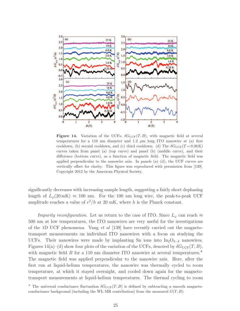
Figure 14. Variation of the UCFs, δGUCF(T,B), with magnetic field at several
temperatures for a 110 nm diameter and 1.2 µm long ITO nanowire at (a) first
cooldown, (b) second cooldown, and (c) third cooldown. (d) The δGUCF(T =0.26K)
curves taken from panel (a) (top curve) and panel (b) (middle curve), and their
difference (bottom curve), as a function of magnetic field. The magnetic field was
applied perpendicular to the nanowire axis. In panels (a)–(d), the UCF curves are
vertically offset for clarity. This figure was reproduced with permission from [139].
Copyright 2012 by the American Physical Society.
significantly decreases with increasing sample length, suggesting a fairly short dephasing
length of Lϕ(20mK) ≈ 100 nm. For the 100 nm long wire, the peak-to-peak UCF
amplitude reaches a value of e2/h at 20 mK, where h is the Planck constant.
Impurity reconfiguration. Let us return to the case of ITO. Since Lϕ can reach ≈500 nm at low temperatures, the ITO nanowires are very useful for the investigations
of the 1D UCF phenomena. Yang et al [139] have recently carried out the magneto-
transport measurements on individual ITO nanowires with a focus on studying the
UCFs. Their nanowires were made by implanting Sn ions into In2O3−δ nanowires.
Figures 14(a)–(d) show four plots of the variation of the UCFs, denoted by δGUCF(T,B),
with magnetic field B for a 110 nm diameter ITO nanowire at several temperatures.∗The magnetic field was applied perpendicular to the nanowire axis. Here, after the
first run at liquid-helium temperatures, the nanowire was thermally cycled to room
temperature, at which it stayed overnight, and cooled down again for the magneto-
transport measurements at liquid-helium temperatures. The thermal cycling to room
∗ The universal conductance fluctuation δGUCF(T,B) is defined by subtracting a smooth magneto-
conductance background (including the WL MR contribution) from the measured G(T,B).
25
temperature was repeated twice, and the sample was thus measured for three times at
three different cooldowns. The idea was that a thermal cycling to 300 K could possibly
induce impurity reconfiguration in the given nanowire. A new impurity configuration
must lead to differing trajectories of the propagating electron partial waves, which in
turn cause distinct quantum interference. As a result, the shape of the UCF patterns
should be completely changed. Figure 14(a) shows δGUCF(T,B) as a function of B at
several temperatures measured at the first cooldown. Figure 14(b) shows δGUCF(T,B)
as a function of B at several temperatures measured at the second cooldown, and
figure 14(c) shows those measured at the third cooldown.
A number of important UCF features and the underlying physics can be learned
from close inspection of these figures.
(i) Inspection of figures 14(a)–(c) indicates that the UCF magnitudes decrease with
increasing temperature and disappear at ∼ 25 K. Thus, these quantum conductance
fluctuations are distinctly different from the classical thermal noise whose resistance
fluctuation magnitudes increase with increasing temperature.
(ii) During a given cooldown, the shape of the UCF patterns at different temperatures
remains the same to a large extent. This observation implies that the impurity
configuration is frozen for a considerable period of time if the nanowire is constantly
kept at liquid-helium temperatures. A given impurity configuration gives rise to
a specific ‘magneto-fingerprint,’ strongly suggesting that the UCF phenomena is a
robust manifestation of an intrinsic quantum-interference effect.
(iii) At a given temperature, the UCFs among different cooldowns reveal similar peak-
to-peak magnitudes.
(iv) Figure 14(d) shows a plot of the δGUCF(T =0.26K,B) curves taken from fig-
ure 14(a) (top curve) and figure 14(b) (middle curve), and their difference (bot-
tom curve). This figure is convenient for close inspection and comparison. The
top two curves reveal completely different shapes of the UCF patterns, strongly
reflecting that a thermal cycling to 300 K has induced an impurity reconfiguration.
On the other hand, the UCF magnitudes of these two curves retain similar, with
a peak-to-peak value of δGUCF(T =0.26K) ≈ 0.5e2/h for both curves. The reason
for retaining a similar UCF magnitude is as follows. The UCF magnitudes in a
given nanowire are governed by the Lϕ values, which are determined by the level of
disorder, i.e., the ρ value (or the R value in 2D), see subsection 3.1.2. The ρ (R)
value of a sample is determined by the total number of impurities, but insensitive
to the specific spatial distribution of the impurities (provided that the impurity
concentration is uniform throughout the sample).♯
Classical self-averaging and thermal averaging at finite temperatures. In the
♯ The UCF studies also allow extractions of the Lϕ(T ) values in a miniature sample. The values thus
obtained are in fair accord with those extracted from the WL MR measurements. In addition to Lϕ,
the thermal diffusion length LT plays a key role in governing the UCF magnitudes.
26
case of a quasi-1D wire with length L, the UCF theory predicts a root-mean-square
conductance fluctuation magnitude of√
〈(δGUCF)2〉 ≃ 0.73e2/h in the limit of T → 0
K [162,163,165]. At this low T limit, the wire behaves as a single phase-coherent regime.
As the temperature gradually increases from absolute zero, Lϕ(T ) becomes progressively
shorter and one has to take into account the classical self-averaging effect. That is,
the phase-coherent regime is expected to be cut off by Lϕ and the UCF magnitude√
〈(δGUCF)2〉 is predicted to be suppressed by a factor (Lϕ/L)3/2 under the condition
Lϕ < LT , where LT =√
D~/kBT ∝ 1/√T is the thermal diffusion length defined
in the EEI theory. The suppression of the UCF magnitudes originates from the fact
that the UCFs of different phase-coherent regimes fluctuate statistically independently.
If the temperature further increases such that LT < Lϕ or, equivalently, the thermal
energy exceeds the Thouless energy kBT > ~/τϕ, one also has to take into account
the thermal averaging effect. That is, the phase-coherent regime is now expected to
be cut off by LT and the UCF magnitude√
〈(δGUCF)2〉 is predicted to be suppressed
by a factor (LT/L)√
Lϕ/L. These theoretical concepts have been well accepted by the
mesoscopic physics communities for three decades, but have rarely been experimentally
tested in a quantitative manner. The lack of experimental information was mainly
due to the fact that the UCFs could be observed only at temperatures below 1 K in
conventional lithographic metal and semiconductor mesoscopic structures. Fortunately,
the observations of the UCFs in ITO nanowires over a wide range of temperature from
below 1 K up to above 10 K now provides us a unique opportunity to verify these subtle
UCF theory predictions.
Figure 15 shows a plot of the variation of measured√
〈(δGUCF)2〉 with temperature
for three ITO nanowires studied by Yang et al [139]. Surprisingly, the theoretical
predictions invoking the thermal averaging effect (dashed curves) diverge significantly
from the measured UCF magnitudes (symbols). In figure 15, the theoretical curves
vary approximately as 1/√T , while the experiment reveals a much slower temperature
dependence. In other words, the phase-coherent regime in the 1D UCF phenomenon is
not cut off by LT , even though the experiment well satisfied the condition kBT > ~/τϕ(LT < Lϕ). The reason why the thermal averaging effect played no significant role
in figure 15 is not understood. The ITO nanowires make experimentally feasible to
reexamine whether any ingredients in the theoretical concepts for thermal averaging in
mesoscopic physics might have been overlooked (overestimated).
In summary, the UCF phenomena manifest rich and subtle quantum-interference
properties of a mesoscopic or nanoscale structure. They provide crucial information
about the impurity configuration in a particular sample. In ITO nanowires, the UCF
signals persist up to 20–30 K. For comparison, recall that in conventional lithographic
metal samples, the UCFs (including magnetic-field dependent UCFs and temporal
UCFs [174]) can only be observed at sub-kelvin temperatures [169]. Such pronounced
conductance fluctuations provide valuable opportunities for critical examinations of the
underlying UCF physics [139, 175]. The presence of marked UCFs suggest that there
must exist a large amount of point defects in artificially synthesized ITO nanostructures,
27

Figure 15. Variation of measured√
〈(δGUCF)2〉 (denoted by the square root of
the variance√
Var(δGUCF) in ordinate) magnitudes with temperature for three ITO
nanowires with diameter and length: circles (110 nm and 1.2 µm), squares (78 nm
and 1.4 µm), and triangles (72 nm, 2.8 µm). The solid curves drawn through the
data points are guides to the eye. The dashed curves are the UCF theory predictions
by taking into account both the classical self-averaging and the thermal averaging
effects. The thermal averaging effect due to LT varies approximately as 1/√T , while
the self-averaging effect due to Lϕ possesses a very weak temperature dependence. The
theoretical and experimental values are normalized for 10 K in each nanowire. Note
that the theoretical predictions diverge significantly from the experimental results.
This figure was reproduced with permission from [139]. Copyright 2012 by the
American Physical Society.
even though the nanowires exhibit a single crystalline structure under high-resolution
transmission electron microscopy studies.††
4. Many-body electron transport in granular metals: Inhomogeneous
indium tin oxide ultrathin films
In this section, we discuss the electrical-transport properties of inhomogeneous
ITO ultrathin films (average thickness ≈ 5–15 nm) which reveal new many-body
physical phenomena that are absent in homogeneous disordered systems. These new
physical properties, including logarithmic temperature dependences of both longitudinal
electrical conductivity and Hall transport in a wide range of temperature, have recently
been theoretically predicted [52–57], but not yet experimentally tested in detail.
Generally speaking, granular metals are composite materials that are composed of
finely dispersed mixtures of immiscible metal and insulator grains. In many cases, the
insulating constituent may form an amorphous matrix [177,178]. In terms of electrical-
transport properties, three distinct regimes can be achieved in a given granular system,
††We note that it has recently been found that high levels of point defects appear in most artificially
grown single-crystalline nanostructures, including ITO, RuO2 [175], and ZnO [176] nanowires.
28

i.e., the metallic, the insulating (dielectric), and the metal-insulator transition regimes.
These three regimes can be conveniently categorized by a quantity called GT . Here GT
is the average tunneling conductance between neighboring (metal) grains and is a key
parameter which determines the global electrical properties of a given granular array.
GT can be expressed in units of e2/~ and written as GT = gT (2e2/~), where ~ is the
Planck constant divided by 2π, and gT is a dimensionless average tunneling conductance.
The factor 2 arises from the two allowed spin directions for a tunneling electron. When
gT > gcT (gT < gcT ) the system lies in the metallic (insulating) regime. A metal-insulator
transition occurs at gT = gcT . Here gcT = (1/2πd) ln(Ec/δ) is a critical dimensionless
tunneling conductance whose value depends on the dimensionality of the granular array
d, where Ec is the charging energy, and δ is the mean energy level spacing in a grain
(references [52,55]). In experiments, the magnitude of gcT is of order unity or somewhat
smaller [109, 179].
Over decades, there has been extensive theoretical and experimental research on
the microstructures and electrical-transport properties of granular systems [178]. New
discoveries have continuously been made and a good understanding of the physical
properties conceptualized. For example, the giant Hall effect (GHE) has recently been
discovered in Cuv(SiO2)1−v [180] and Mov(SnO2)1−v [181] granular films under the
conditions that the grain size a ≪ Lϕ and the metal volume fraction v is around
the quantum percolation threshold vq [182]. The GHE is a novel physical phenomenon
which manifests a huge Hall coefficient RH that is enhanced by ∼ 3 orders of magnitude
when v approaches vq from the metallic side. The GHE is theoretically explained to
arise from the local quantum-interference effect in the presence of rich microstructures in
a metal-insulator composite constituting of nanoscale granules [182]. While the single-
particle local quantum interference causes the new GHE, in the following discussion we
shall focus on the many-body electronic transport properties in granular systems.
In the rest of this section, we concentrate on the region with gT ≫ 1 or gT ≫ gcT .
The material systems that we are interested in can thus be termed ‘granular metals.’
In particular, we shall demonstrate that inhomogeneous ITO ultrathin films are an
ideal granular metal system which provides valuable and unique playgrounds for
critically testing the recent theories of granular metals. These new theories of granular
metals are concerned with the many-body electron-electron (e-e) interaction effect in
inhomogeneous disordered systems. They focus on the electronic conduction properties
in the temperature regime above moderately low temperatures (T > gT δ/kB) where the
WL effect is predicted to be comparatively small or negligible [52, 183]. In practice,
one can explicitly measure the e-e interaction effect by applying a weak perpendicular
magnetic field to suppress the quantum-interference WL effect.
4.1. Longitudinal electrical conductivity
For a long time, the electrical-transport properties of granular metals have not been
explicitly considered theoretically. It has widely been taken for granted that the
29
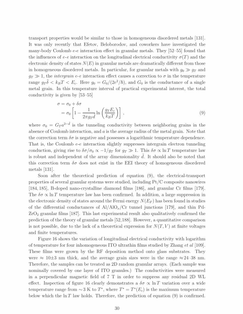
transport properties would be similar to those in homogeneous disordered metals [131].
It was only recently that Efetov, Beloborodov, and coworkers have investigated the
many-body Coulomb e-e interaction effect in granular metals. They [52–55] found that
the influences of e-e interaction on the longitudinal electrical conductivity σ(T ) and the
electronic density of states N(E) in granular metals are dramatically different from those
in homogeneous disordered metals. In particular, for granular metals with g0 ≫ gT and
gT ≫ 1, the intergrain e-e interaction effect causes a correction to σ in the temperature
range gT δ < kBT < Ec. Here g0 = G0/(2e2/~), and G0 is the conductance of a single
metal grain. In this temperature interval of practical experimental interest, the total
conductivity is given by [53–55]
σ = σ0 + δσ
= σ0
[
1− 1
2πgT dln
(
gTEc
kBT
)]
, (9)
where σ0 = GTa2−d is the tunneling conductivity between neighboring grains in the
absence of Coulomb interaction, and a is the average radius of the metal grain. Note that
the correction term δσ is negative and possesses a logarithmic temperature dependence.
That is, the Coulomb e-e interaction slightly suppresses intergrain electron tunneling
conduction, giving rise to δσ/σ0 ∝ −1/gT for gT ≫ 1. This δσ ∝ lnT temperature law
is robust and independent of the array dimensionality d. It should also be noted that
this correction term δσ does not exist in the EEI theory of homogeneous disordered
metals [131].
Soon after the theoretical prediction of equation (9), the electrical-transport
properties of several granular systems were studied, including Pt/C composite nanowires
[184, 185], B-doped nano-crystalline diamond films [186], and granular Cr films [179].
The δσ ∝ lnT temperature law has been confirmed. In addition, a large suppression in
the electronic density of states around the Fermi energy N(EF ) has been found in studies
of the differential conductances of Al/AlOx/Cr tunnel junctions [179], and thin Pd-
ZrO2 granular films [187]. This last experimental result also qualitatively confirmed the
prediction of the theory of granular metals [52,188]. However, a quantitative comparison
is not possible, due to the lack of a theoretical expression for N(T, V ) at finite voltages
and finite temperatures.
Figure 16 shows the variation of longitudinal electrical conductivity with logarithm
of temperature for four inhomogeneous ITO ultrathin films studied by Zhang et al [109].
These films were grown by the RF deposition method onto glass substrates. They
were ≈ 10±3 nm thick, and the average grain sizes were in the range ≈ 24–38 nm.
Therefore, the samples can be treated as 2D random granular arrays. (Each sample was
nominally covered by one layer of ITO granules.) The conductivities were measured
in a perpendicular magnetic field of 7 T in order to suppress any residual 2D WL
effect. Inspection of figure 16 clearly demonstrates a δσ ∝ lnT variation over a wide
temperature range from ∼ 3 K to T ∗, where T ∗ = T ∗(Ec) is the maximum temperature
below which the lnT law holds. Therefore, the prediction of equation (9) is confirmed.
30

Figure 16. Variation of longitudinal electrical conductivity with logarithm of
temperature for four inhomogeneous ITO ultrathin films measured in a perpendicular
magnetic field of 7 T. The average film thickness (in nm), average grain size (in nm)
and fitted gT value in each film are (a) 9.2, 28 and 13, (b) 11, 34 and 23, (c) 13,
38 and 31, and (d) 7.6, 24 and 7.4. The solid straight lines are least-squares fits to
equation (9). This figure was reproduced with permission from [109]. Copyright 2011
by the American Physical Society.
Quantitatively, from the least-squares fits (the straight solid lines in figure 16), values
of the intergrain tunneling conductance gT ≃ 7–31 were obtained. Therefore, the
theoretical criterion of gT ≫ 1 for equation (9) to be valid is satisfied. We reiterate
that the δσ ∝ lnT temperature law observed in figure 16 is not due to the more familiar
2D EEI effect which widely appears in homogeneous disordered systems [109].
4.2. Hall transport
Apart from the longitudinal electrical conductivity, Kharitonov and Efetov [56, 57]
have investigated the influence of Coulomb interaction on the Hall resistivity, ρxy, by
taking the electron dynamics inside individual grains into account. They found that
there also exists a correction to the Hall resistivity in the wide temperature range
gT δ . kBT . min(gTEc, ETh), where ETh = D0~/a2 is the Thouless energy of a grain
of radius a, D0 is the electron diffusion constant in the grain, and min(gTEc, ETh)
denotes the minimum value of the set (gTEc, ETh). The resulting Hall resistivity is
given by [56, 57]
ρxy(T ) = ρxy,0 + δρxy
=B
n∗e
[
1 +cd
4πgTln
(
min(gTEc, ETh)
kBT
)]
, (10)
where n∗ is the effective carrier concentration, cd is a numerical factor of order unity,
and ρxy,0 = B/(n∗e) is the Hall resistivity of the granular array in the absence of the
31
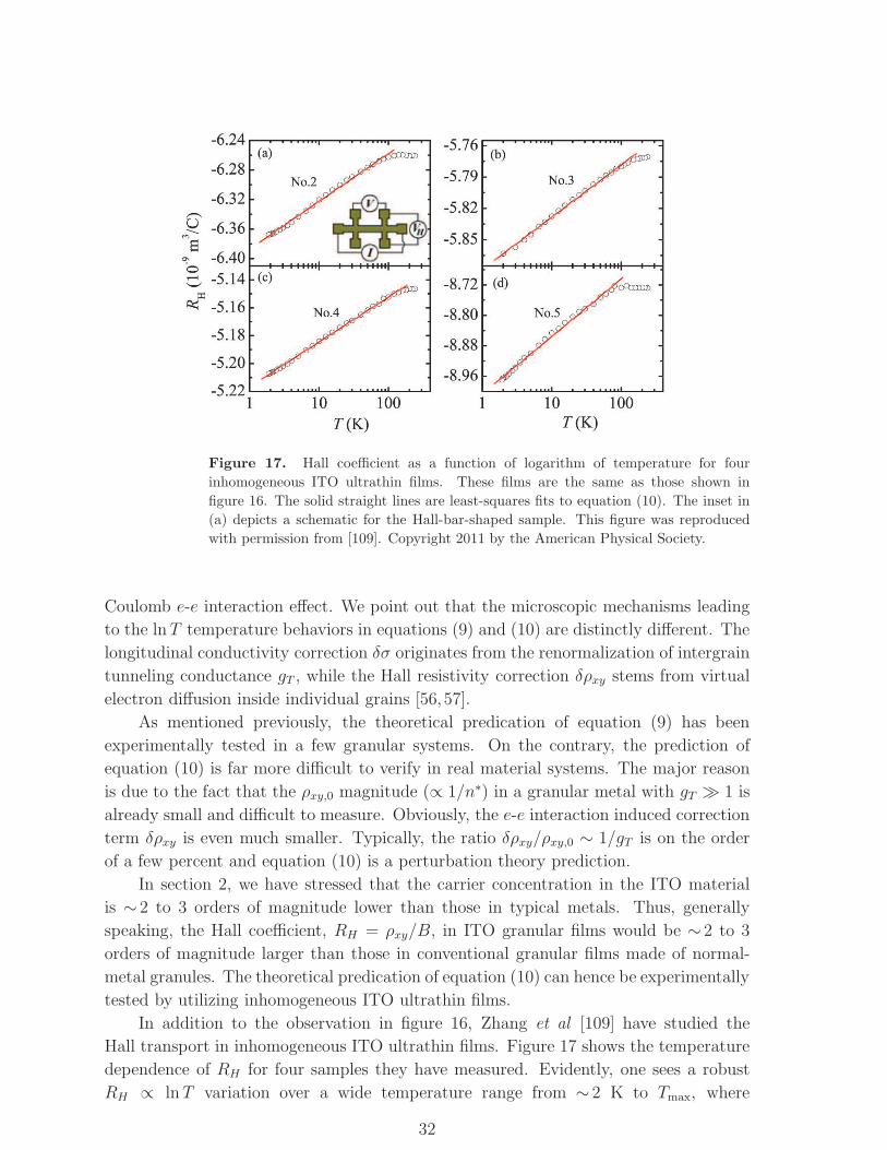
Figure 17. Hall coefficient as a function of logarithm of temperature for four
inhomogeneous ITO ultrathin films. These films are the same as those shown in
figure 16. The solid straight lines are least-squares fits to equation (10). The inset in
(a) depicts a schematic for the Hall-bar-shaped sample. This figure was reproduced
with permission from [109]. Copyright 2011 by the American Physical Society.
Coulomb e-e interaction effect. We point out that the microscopic mechanisms leading
to the lnT temperature behaviors in equations (9) and (10) are distinctly different. The
longitudinal conductivity correction δσ originates from the renormalization of intergrain
tunneling conductance gT , while the Hall resistivity correction δρxy stems from virtual
electron diffusion inside individual grains [56, 57].
As mentioned previously, the theoretical predication of equation (9) has been
experimentally tested in a few granular systems. On the contrary, the prediction of
equation (10) is far more difficult to verify in real material systems. The major reason
is due to the fact that the ρxy,0 magnitude (∝ 1/n∗) in a granular metal with gT ≫ 1 is
already small and difficult to measure. Obviously, the e-e interaction induced correction
term δρxy is even much smaller. Typically, the ratio δρxy/ρxy,0 ∼ 1/gT is on the order
of a few percent and equation (10) is a perturbation theory prediction.
In section 2, we have stressed that the carrier concentration in the ITO material
is ∼ 2 to 3 orders of magnitude lower than those in typical metals. Thus, generally
speaking, the Hall coefficient, RH = ρxy/B, in ITO granular films would be ∼ 2 to 3
orders of magnitude larger than those in conventional granular films made of normal-
metal granules. The theoretical predication of equation (10) can hence be experimentally
tested by utilizing inhomogeneous ITO ultrathin films.
In addition to the observation in figure 16, Zhang et al [109] have studied the
Hall transport in inhomogeneous ITO ultrathin films. Figure 17 shows the temperature
dependence of RH for four samples they have measured. Evidently, one sees a robust
RH ∝ lnT variation over a wide temperature range from ∼ 2 K to Tmax, where
32

Tmax is a temperature below which the lnT law holds. The Tmax value for a given
granular array is determined by the constituent grain parameters Ec and ETh as well
as the intergrain tunneling parameter gT . For those ITO ultrathin films shown in
figure 17, the experimental Tmax values varied from ∼ 50 to ∼ 120 K. Quantitatively, the
correction term contributes a small magnitude of [RH(2K) − RH(Tmax)]/RH(Tmax) ≃δρxy(2K)/ρxy,0 . 5%, where RH(Tmax) ≃ 1/(n∗e) is the Hall coefficient in the absence
of the Coulomb e-e interaction effect. The experimental data (symbols) can be well
described by the theoretical predictions (solid straight lines) with satisfactory values
of the adjustable parameters. Thus, the prediction of equation (10) is experimentally
confirmed for the first time in the literature.
In summary, the simultaneous experimental observations of δσ ∝ lnT (figure 16)
and δρxy ∝ lnT (figure 17) laws over a wide range of temperature from liquid-
helium temperature up to and above liquid-nitrogen temperature strongly support the
recent theoretical concepts for charge transport in granular metals, i.e., equations (9)
and (10), which are formulated under the condition that the intergrain tunneling
conductivity gT ≫ 1. We note again that the free-carrier-like and, especially, the low-n
characteristics of the ITO material have made possible a close experimental examination
of equation (10). While measurements of δσ are relatively easy, finding a proper granular
metal with gT ≫ 1 to measure the small correction term δρxy is definitely nontrivial. The
ITO material made into an inhomogeneous ultrathin film form has opened up avenues
for exploring the many-body Coulomb effects in condensed matter physics.
Recently, the thermoelectric power in the presence of granularity and in the limit
of gT ≫ 1 has been theoretically calculated [189]. It was predicted that the granularity
could lead to substantial improvement in thermodynamic properties and, in particular,
the figure of merit of granular materials could be high. Experimental investigations in
this direction would be worthwhile in light of the development of useful thermoelectric
materials. On the other hand, it has recently been reported that the presence of
granularity causes an enhancement of the flicker noise (1/f noise) level in ITO films.
This is ascribed to atomic diffusion along grain boundaries or dynamics of two-level
systems near the grain boundaries [190]. Since the 1/f noise could potentially hinder
the miniature device performance, it would be of interest and importance to explore its
properties in inhomogeneous ITO ultrathin films.
5. Conclusion
Indium tin oxide (ITO) is a very interesting and useful transparent conducting oxide
(TCO) material. It is stable at ambient conditions and can be readily grown into a
variety of forms, including polycrystalline thin and thick films, and single-crystalline
nanowires. They can simultaneously have electrical resistivities as low as ≈ 150 µΩcm
at room temperature and optical transparencies as high as ≈ 90% transmittance at the
visible light frequencies. Apart from their technological issues, the electronic conduction
properties of ITO have rarely been systematically explored as a condensed matter
33
physics research subject and down to fundamental levels. In this Topical Review, we
have focused on metallic ITO structures. We have shown that the overall electrical
resistivity and thermoelectric power can be described by the Boltzmann transport
equation. A linear dependence on temperature of thermoelectric power in a wide range
of temperature eloquently manifests the free-carrier-like energy bandstructure around
the Fermi level of this class of material. At liquid-helium temperatures, marked weak-
localization effect and universal conductance fluctuations emerge. ITO provides a rich
playground for studying these quantum interference phenomena in all three dimensions,
which leads to an improved understanding of the underlying physics governing the
properties of mesoscopic and nanoscale structures. Inhomogeneous ITO ultrathin films
have opened up unique and valuable avenues for studying the many-body electron-
electron interaction effect in granular metals. These new theoretical predictions cannot
be addressed by employing conventional granular systems.
The objective of this Topical Review is not only to present the charge transport
properties of ITO but also to demonstrate that the ITO material is versatile and
powerful for unraveling new physics. Microscopically, the intrinsic electronic properties
that make ITO an appealing technological as well as academic material are the free-
carrier-like energy bandstructure and a low level of carrier concentration. Owing to
the inherent free-carrier-like characteristics, the electronic parameters can be reliably
evaluated through the free-electron model, which in turn facilitate critical tests of a
variety of lasting and new theoretical predictions. A low carrier concentration gives
rise to slow electron-phonon relaxation, which manifests the linear electron diffusion
thermoelectric power and also yields a weak electron dephasing rate in the ITO material.
In light of the development and search for useful TCOs, it would be of great interest to
investigate whether the numerous aspects of the novel electronic conduction properties
that we have addressed in this Topical Review might also manifest in other, such as
ZnO- and SnO2-based, TCO materials.
Acknowledgments
The authors thank Yuri Galperin, Andrei Sergeev, and Igor Beloborodov for valuable
suggestions and comments, and David Rees for careful reading of the manuscript. We
are grateful to Shao-Pin Chiu, Yi-Fu Chen, Chih-Yuan Wu, Yao-Wen Hsu, Bo-Tsung
Lin, Ping-Yu Yang, and Yu-Jie Zhang for their collaborations at the various stages of
our lasting research on ITO. One of us (JJL) also would like to thank Hsin-Fei Meng
for incidentally igniting his interest in the marvelous electronic conduction properties
of the ITO material a decade ago. This work was supported at NCTU by the Taiwan
Ministry of Science and Technology through Grant No. NSC 102-2120-M-009-003 and
the MOE ATU Program, and at TJU by the NSF of China through Grant No. 11174216
and the Research Fund for the Doctoral Program of Higher Education through Grant
No. 20120032110065.
34

References
[1] Holland L 1956 Vacuum Deposition of Thin Films (New York: Wiley) p. 492
[2] Jarzebski Z M 1982 Phys. Stat. Sol. (a) 71 13
[3] Facchetti A and Marks T J 2010 Transparent Electronics: From Synthesis to Applications (Wiley,
United Kingdom)
[4] Ginley D S and Bright C 2000 MRS Bull. 25 15
[5] Granqvist C G and Hultaker A 2002 Thin Solid Films 411 1
[6] Granqvis C G 2007 Sol. Energy Mater. Sol. Cells 91 1529
[7] Hamberg I, Granqvist C G, Berggren K F, Sernelius B E and Engstrom L 1984 Phys. Rev. B 30
3240
[8] Gerfin T and Gratzel M 1996 J. Appl. Phys. 79 1722
[9] Schroer P, Kruger P and Pollmann J 1993 Phys. Rev. B 47 6971
[10] Imai Y J, Watanabe A and Shimono I 2003 J. Mater. Sci.: Mater. Electr. 14 149
[11] Imai Y J and Watanabe A 2004 J. Mater. Sci.: Mater. Electr. 15 743
[12] Karazhanov S Z, Ravindran P, Kjekshus A, Fjellvag H and Svensson B G 2007 Phys. Rev. B 75
155104
[13] Kılıc C and Zunger A 2002 Phys. Rev. Lett. 88 095501
[14] Robertson J 1984 Phys. Rev. B 30 3520
[15] Mishra K C, Johnson K H and Schmidt P C 1995 Phys. Rev. B 51 13972
[16] Li Z Q, Yin Y L, Liu X D and Song Q G 2009 J. Appl. Phys. 106 083701
[17] Schleife A, Varley J B, Fuchs F, Rodl C, Bechstedt F, Rinke P, Janotti A and Van de Walle C G
2011 Phys. Rev. B 83 035116
[18] Liu X D, Jiang E Y, Li Z Q and Song Q G 2008 Appl. Phys. Lett. 92 252104
[19] Osorio-Guillen J, Lany S and Zunger A 2008 Phys. Rev. Lett. 100 036601
[20] Orita N 2010 Japn. J. Appl. Phys. 49 055801
[21] Chen D M, Xu G, Miao L, Chen L H, Nakao S and Jin P 2010 J. Appl. Phys. 107 063707
[22] Huy H A, Aradi B, Frauenheim T and Deak P 2011 Phys. Rev. B 83 155201
[23] Yamamoto T and Ohno T 2012 Phys. Rev. B 85 033104
[24] Yang Y, Jin S, Medevdeva J E, Ireland J R, Metz A W, Ni J, Hersam M C, Freeman A J and
Marks T J 2005 J. Am. Chem. Soc. 127 8796
[25] Medevdeva J E and Freeman A J 2005 Europhys. Lett. 69 583
[26] Odaka H, Shigesato Y, Murakami T and Iwata S 2001 Jpn. J. Appl. Phys. (Part 1) 40 3231
[27] Mryasov O N and Freeman A J 2001 Phys. Rev. B 64 233111
[28] Medvedeva J E 2006 Phys. Rev. Lett. 97 086401
[29] Medvedeva J E and Hettiarachchi C L 2010 Phys. Rev. B 81 125116
[30] King P D C, Veal T D, Payne D J, Bourlange A, Egdell R G and McConville C F 2008 Phys. Rev.
Lett. 101 116808
[31] King P D C, Veal T D, McConville C F, Zuniga Perez J, Munoz Sanjose V, Hopkinson M, Rienks
E D L, JensenM F and Hofmann P 2010 Phys. Rev. Lett. 104 256803
[32] Lany S, Zakutayev A, Mason T O, Wager J F, Poeppelmeier K R, Perkins J D, Berry J J, Ginley
D S and Zunger A 2012 Phys. Rev. Lett. 108 016802
[33] Zhang K H L, Egdell R G, Offi F, Iacobucci S, Petaccia L, Gorovikov S and King P D C 2013
Phys. Rev. Lett. 110 056803
[34] Taga N, Shigesato Y and Kamei M 2000 J. Vac. Sci. Technol. A 18 1663
[35] Rauf I A 1996 J. Appl. Phys. 79 4057
[36] Kittel C 2005 Introduction to Solid State Physics 8th edn (New York: Wiley)
[37] Lin J J, Yu C and Yao Y D 1993 Phys. Rev. B 48 4864
[38] Hsu S Y, Sheng P J and Lin J J 1999 Phys. Rev. B 60 3940
[39] Guillen C and Herrero J 2007 J. Appl. Phys. 101 073514
[40] Kim H, Gilmore C M, Pique A, Horwitz J S, Mattoussi H, Murata H, Kafafi Z H and Chrisey D
35
B 1999 J. Appl. Phys. 86 6451
[41] Chopra K L, Major S and Pandya D K 1983 Thin Solid Films 102 1
[42] Hamberg I and Granqvist C G 1986 J. Appl. Phys. 60 R123
[43] Lewis B G and Paine D C 2000 MRS Bull. 25 22
[44] Kawazoe K, Yanagi H, Ueda K and Hosono H 2000 MRS Bull. 25 28
[45] Minami T 2000 MRS Bull. 25 38
[46] Freeman A J, Poeppelmeier K R, Mason T O, Chang R P H and Marks T J 2000 MRS Bull. 25
45
[47] Gordon R G 2000 MRS Bull. 25 52
[48] Coutts T J, Young D L and Li X 2000 MRS Bull. 25 58
[49] Exarhos G J and Zhou X D 2007 Thin Solid Films 515 7025
[50] Hosono H 2007 Thin Solid Films 515 6000
[51] King P D C and Veal T D 2011 J. Phys.: Condens. Matter 23 334214.
[52] Beloborodov I S, Lopatin A V, Vinokur V M and Efetov K B 2007 Rev. Mod. Phys. 79 469
[53] Efetov K B and Tschersich A 2003 Phys. Rev. B 67 174205
[54] Efetov K B and Tschersich A 2002 Europhys. Lett. 59 114
[55] Beloborodov I S, Efetov K B, Lopatin A V and Vinokur V M 2003 Phys. Rev. Lett. 91 246801
[56] Kharitonov M Yu and Efetov K B 2007 Phys. Rev. Lett. 99 056803
[57] Kharitonov M Yu and Efetov K B 2008 Phys. Rev. B 77 045116
[58] Liu C, Matsutani T, Asanuma T, Murai M, Kiuchi M, Alves E and Reis M 2003 J. Appl. Phys.
93 2262
[59] Iwatsubo S 2006 Vacuum 80 708
[60] Shigesato Y, Koshi-ishi R, Kawashima T and Ohsako J 2000 Vacuum 59 614
[61] Liu X D, Jiang E Y and Zhang D X 2008 J. Appl. Phys. 104 073711
[62] Kytin V G, Kulbachinskii V A, Reukova O V, Galperin Y M, Johansen T H, Diplas S and Ulyashin
A G 2014 Appl. Phys. A: Materials Science & Processing 114 957
[63] Mott N F and Davis E A 1979 Electronic Processes in Non-Crystalline Materials 2nd edn
(Clarendon: Oxford)
[64] Shklovskii B I and Efros A L 1984 Electronic Properties of Doped Semiconductors (Berlin: Springer-
Verlag)
[65] Sheng P, Abeles B and Arie Y 1973 Phys. Rev. Lett. 31 44
[66] Beloborodov I S, Lopatin A V and Vinokur V M 2005 Phys. Rev. B 72 125121
[67] Ohyama T, Okamoto M and Otsuka E 1985 J. Phys. Soc. Jpn. 54 1041
[68] Mori N 1993 J. Appl. Phys. 73 1327
[69] Chiu S P, Chung H F, Lin Y H, Kai J J, Chen F R and Lin J J 2009 Nanotechnology 20 105203
[70] Aliev A E, Xiong K, Cho K and Salamon M B 2012 Appl. Phys. Lett. 101 252603
[71] Fan J C C and Goodenough J B 1977 J. Appl. Phys. 48 3524
[72] Fuchs F and Bechstedt F 2008 Phys. Rev. B 77 155107
[73] Kikuchi N, Kusano E, Nanto H, Kinbara A and Hosono H 2000 Vacuum 59 492
[74] Huang K F, Uen T M, Gou Y S, Huang C R and Yan H C 1987 Thin Solid Films 148 7
[75] Shigesato Y, Paine D C and Haynes T E 1993 J. Appl. Phys. 73 3805
[76] Taga N, Odaka H, Shigesato Y, Yasui I, Kamei M and Haynes T E 1996 J. Appl. Phys. 80 978
[77] Mizuhashi M 1980 Thin Solid Films 70 91
[78] Agnihotry S A, Saini K K, Saxena T K, Nagpal K C and Chandra S 1985 J. Phys. D 18 2087
[79] Jan S W and Lee S C 1987 J. Electrochem. Soc. 134 2056
[80] Nanto H, Minami T, Orito S and Takata S 1988 J. Appl. Phys. 63 2711
[81] Wu W F and Chiou B S 1994 Thin Solid Films 247 201
[82] Joshi R N, Singh V P and McClure J C 1995 Thin Solid Films 257 32
[83] Wu C Y, Lin B T, Zhang Y J and Lin J J 2012 Phys. Rev. B 85 104204
[84] Kane J and Schweizer H P 1975 Thin Solid Films 29 155
[85] Ryabova L A, Salun V S and Serbinov I A 1982 Thin Solid Films 92 327
36
[86] Maruyama T and Fukui K 1991 Thin Solid Films 203 197
[87] Xu J J, Shaikh A S and Vest R W 1988 Thin Solid Films 161 273
[88] Furusaki T and Kodaira K 1991 High Performance Ceramic Films and Coatings ed Vincenzini P
(Amsterdam: Elsevier) p. 241
[89] Nishio K, Sei T and Tsushiya T 1996 J. Mater. Sci. 31 1761
[90] Alam M J and Cameron D C 2000 Thin Solid Films 377–378 455
[91] Ramaiah K S, Raja V S, Bhatnagar A K, Tomlinson R D, Pilkington R D, Hill A E, Chang S J,
Su Y K and Juang F S 2000 Semic. Sci. Technol. 15 676
[92] Hichoua A El, Kachouaneb A, Bubendorffc J L, Addoub M, Ebothec J, Troyonc M and Bougrine
A 2004 Thin Solid Films 458 263
[93] Moholkar A V, Pawar S M, Rajpure K Y, Ganesan V and Bhosale C H 2008 J. Alloy. Compd.
464 387
[94] Guo E J, Guo H, Lu H, Jin K, He M and Yang G 2011 Appl. Phys. Lett. 98 011905
[95] Bierwagen O and Speck J S 2014 Phys. Stat. Sol. (a) 211 48
[96] Ohta H, Orita M, Hirano M, Tanji H, Kawazoe H and Hosono H 2000 Appl. Phys. Letts. 76 2740
[97] Nistor M, Perriere J, Hebert C and Seiler W 2010 J. Phys.: Condens. Matter 22 045006
[98] Seiler W, Nistor M, Hebert C and Perriere J 2013 Sol. Energy Mater. Sol. Cells 116 34
[99] Li Z Q and Lin J J 2004 J. Appl. Phys. 96 5918
[100] Zhong Y L and Lin J J 1998 Phys. Rev. Lett. 80 588
[101] Zhong Y L, Sergeev A, Chen C D and Lin J J 2010 Phys. Rev. Lett. 104 206803
[102] Wu C Y, Jian W B and Lin J J 1998 Phys. Rev. B 57 11232
[103] Lin B T, Chen Y F, Lin J J and Wu C Y 2010 Thin Solid Films 518 6997
[104] Preissler N, Bierwagen O, Ramu A T and Speck J S 2013 Phys. Rev. B 88 085305
[105] Ederth J, Johnsson P, Niklasson G A, Hoel A, Hultaker A, Heszler P, Granqvist C G, van Doorn
A R and Jongerius M J 2003 Phys. Rev. B 68 155410
[106] Sheng P, Sichel E K and Gittleman J I 1978 Phys. Rev. Lett. 40 1197
[107] Sheng P 1980 Phys. Rev. B 21 2180
[108] Lin Y H, Chiu S P and Lin J J 2008 Nanotechnology 19 365201
[109] Zhang Y J, Li Z Q and Lin J J 2011 Phys. Rev. B 84 052202
[110] Bamiduro O, Mustafa H, Mundle R, Konda R B and Pradhan A K 2007 Appl. Phys. Lett. 90
252108
[111] Liu X D, Liu J, Chen S and Li Z Q 2012 Appl. Surf. Sci. 263 486
[112] Yang Y, Zhang Y J, Liu X D and Li Z Q 2012 Appl. Phys. Lett. 100 262101
[113] Bhosle V, Tiwari A and Narayan J 2006 Appl. Phys. Lett. 88 032106
[114] Ahn B D, Oh S H, Kim H J, Jung M H and Ko Y G 2007 Appl. Phys. Lett. 91 252109
[115] Furubayashi Y, Hitosugi T, Yamamoto Y, Inaba K, Kinoda G, Hirose Y, Shimada T and Hasegawa
T 2005 Appl. Phys. Lett. 86 252101
[116] Zheng X W and Li Z Q 2009 Appl. Surf. Sci. 255 8104
[117] Amorim C A, Dalmaschio C J, Melzi A L R, Leite E R and Chiquito A J 2014 J. Phys. Chem.
Solids 75 583
[118] Lang W J and Li Z Q 2014 (arXiv:1406.5269)
[119] MacDonald D K C 1962 Thermoelectricity: An Introduction to the Principles (New York: Wiley)
[120] Siebold T and Ziemann P 1995 Phys. Rev. B 51 6328
[121] Wu C Y, Thanh T V, Chen Y F, Lee J K, and Lin J J 2010 J. Appl. Phys. 108 123708
[122] Guilmeau E, Berardan D, Simon C, Maignan A, Raveau B, Ovono D O and Delorme F, 2009 J.
Appl. Phys. 106 053715
[123] Blatt F J 1970 Physics of Electronic Conduction in Solids (New York: McGraw-Hill)
[124] Reizer M Yu and Sergeev A V 1986 Sov. Phys.–JETP 63 616
[125] Sergeev A V and Reizer M Yu 1996 Int. J. Mod. Phys. B 10 635
[126] Ashida T, Miyamura A, Oka N, Sato Y, Yagi T, Taketoshi N, Baba T and Shigesato Y 2009 J.
Appl. Phys. 105 073709
37
[127] Cordfunke E H P and Westrum Jr E F 1992 J. Phys. Chem. Solids 53 361
[128] Wang L M, Chang C Y, Yeh S T, Chen S W, Peng Z A, Bair S C, Lee D S, Liao F C and Kuo
Y K 2012 Ceram. Int. 38 1167
[129] Wu C Y, Lin B T, Zhang Y J, Li Z Q, and Lin J J 2012 Phys. Rev. B 85 104204
[130] Bergmann G 1984 Phys. Rep. 107 1
[131] Altshuler B L and Aronov A G 1985 Electron–Electron Interactions in Disordered Systems ed A
L Efros and M Pollak (Amsterdam: Elsevier)
[132] Fukuyama H 1985 Electron–Electron Interactions in Disordered Systems ed A L Efros and M
Pollak (Amsterdam: Elsevier)
[133] Lee P A and Ramakrishnan T V 1985 Rev. Mod. Phys. 57 287
[134] Chakravarty S and Schmid A 1986 Phys. Rep. 140 193
[135] Lin J J and Bird J P 2002 J. Phys.: Condens. Matter 14 R501
[136] Ohyama T, Okamoto M and Otsuka E 1983 J. Phys. Soc. Jpn. 52 3571
[137] Chiquito A J, Lanfredi A J C, de Oliveira R F M, Pozzi L P and Leite E R 2007 Nano Lett. 7
1439
[138] Hsu Y W, Chiu S P, Lien A S and Lin J J 2010 Phys. Rev. B 82 195429
[139] Yang P Y, Wang L Y, Hsu Y W and Lin J J 2012 Phys. Rev. B 85 085423
[140] Zhang Y J, Li Z Q and Lin J J 2013 Europhys. Lett. 103 47002
[141] Liu X D, Jiang E Y and Li Z Q 2007 J. Appl. Phys. 102 073708
[142] Shinozaka B, Makise K, Shimane Y, Nakamura H and Inoue K 2007 J. Phys. Soc. Jap. 76 074718
[143] Chiu S P, Lu J G and Lin J J 2013 Nanotechnology 24 245203
[144] Altshuler B L, Aronov A G and Khmelnitsky D E 1982 J. Phys. C 15 7367
[145] Rammer J and Schmid A 1986 Phys. Rev. B 34 1352
[146] Fukuyama H and Abrahams E 1983 Phys. Rev. B 27 5976
[147] Pierre F, Gougam A B, Anthore A, Pothier H, Esteve D and Birge N O 2003 Phys. Rev. B 68
085413
[148] Lin J J and Giordano N 1987 Phys. Rev. B 35 1071
[149] Huang S M, Lee T C, Akimoto H, Kono K and Lin J J 2007 Phys. Rev. Lett. 99 046601
[150] Lin J J, Li T J and Zhong Y L 2003 J. Phys. Soc. Jpn. 72 Suppl. A 7
[151] Golubev D S and Zaikin A D 2007 Physica E 40 32
[152] Rotter I 2009 J. Phys. A 42 153001
[153] Schmid A 1974 Z. Phys. 271 251.
[154] Altshuler B L and Aronov A G 1979 JETP Lett. 30 482
[155] Sergeev A and Mitin V 2000 Phys. Rev. B 61 6041
[156] Wen B, Yakobov R, Vitkalov S A and Sergeev A 2013 Appl. Phys. Lett. 103 222601
[157] Hsu S Y, Sheng P J and Lin J J 1999 Phys. Rev. B 60 3940
[158] Li L, Lin S T, Dong C and Lin J J 2006 Phys. Rev. B 74 172201
[159] Bergmann G and Horriar-Esser C 1985 Phys. Rev. B 31 1161
[160] Zutic I, Fabian J and Sarma S D 2004 Rev. Mod. Phys. 76 323
[161] Shinozaki B, Hidaka K, Ezaki S, Makise K, Asano T, Tomai S, Yano K and Nakamura H 2013
J. Appl. Phys. 113 153707
[162] Lee P A and Stone A D 1985 Phys. Rev. Lett. 55 1622
[163] Lee P A, Stone A D and Fukuyama H 1987 Phys. Rev. B 35 1039
[164] Washburn S and Webb R A 1986 Adv. Phys. 35 375
[165] Beenakker C W J and van Houten H 1988 Phys. Rev. B 37 6544
[166] Washburn S and Webb R A 1992 Rep. Prog. Phys. 55 1311
[167] Thornton T J, Pepper M, Ahmed H, Davies G J and Andrews D 1987 Phys. Rev. B 36 4514(R)
[168] Hansen A E, Bjork M T, Fasth C, Thelander C and Samuelson L 2005 Phys. Rev. B 71 205328
[169] Wagner K, Neumaier D, Reinwald M, Wegscheider W and Weiss D 2006 Phys. Rev. Lett. 97
056803
[170] Man H T and Morpurgo A F 2005 Phys. Rev. Lett. 95 026801
38
[171] Berezovsky J, Borunda M F, Heller E J and Westervelt R M 2010 Nanotechnology 21 274013
[172] Checkelsky J G, Hor Y S, Cava R J and Ong N P 2011 Phys. Rev. Lett. 106 196801
[173] Chiu S P and Lin J J 2013 Phys. Rev. B 87 035122
[174] Beutler D E, Meisenheimer T L and Giordano N 1987 Phys. Rev. Lett. 58 1240
[175] Lien A S, Wang L Y, Chu C S and Lin J J 2011 Phys. Rev. B 84 155432
[176] Chiu S P, Lin Y H and Lin J J 2009 Nanotechnology 20 015203
[177] Abeles B, Sheng P, Coutts M D and Arie Y 1975 Adv. Phys. 24 407
[178] Abeles B 1976 Applied Solid State Science: Advance in Materials and Device Research ed Wolf
R (New York San Franciso London: Academic Press)
[179] Sun Y C, Yeh S S and Lin J J 2010 Phys. Rev. B 82 054203
[180] Zhang X X, Wan C, Liu H, Li Z Q, Sheng P and J. J. Lin 2001 Phys. Rev. Lett. 86 5562
[181] Wu Y N, Li Z Q and Lin J J 2011 Phys. Rev. B 82 092202
[182] Wan C and Sheng P 2002 Phys. Rev. B 66 075309
[183] Beloborodov I S, Lopatin A V, Schwiete G and Vinokur V M 2004 Phys. Rev. B 70 073404
[184] Rotkina L, Oh S, Eckstein J N and Rotkin S V 2005 Phys. Rev. B 72 233407
[185] Sachser R, Porrati F, Schwalb C H and Huth M 2011 Phys. Rev. Lett. 107 206803
[186] Achatz P, GajewskiW, Bustarret E, Marcenat C, Piquerel R, Chapelier C, Dubouchet T, Williams
O A, Haenen K, Garrido J A and Stutzmann M 2009 Phys. Rev. B 79 201203
[187] Bakkali H and Dominguez M 2013 Europhys. Lett. 104 17007
[188] Beloborodov I S, Lopatin A V and Vinokur V M 2004 Phys. Rev. B 70 205120
[189] Glatz A and Beloborodov I S 2009 Phys. Rev. B 79 041404(R)
[190] Yeh S S, Hsu W M, Lee J K, Lee Y J and Lin J J 2013 Appl. Phys. Lett. 103 123118
39