Embed Size (px)
Citation preview

Electronic Computer-Aided Design
Supplement to PHYS3360/AEP3630 Laboratory Manual
Ivan V. Bazarov
Physics DepartmentCornell University
October 6, 2009
Contents
1 Introduction To Electronic Computer-Aided Design 3
1.1 About SPICE and LTspice . . . . . . . . . . . . . . . . . . . . . . . 51.2 Getting Started with LTspice . . . . . . . . . . . . . . . . . . . . . . 7
1.2.1 Example 1: High-Pass Filter . . . . . . . . . . . . . . . . . . . 71.2.2 Example 2: Simplistic Op-Amp . . . . . . . . . . . . . . . . . 151.2.3 Example 3: Using External Models . . . . . . . . . . . . . . . 211.2.4 Example 4: Creating Custom Components . . . . . . . . . . . 26
1.3 Practice Problems . . . . . . . . . . . . . . . . . . . . . . . . . . . . . 32
2 Optional Experiments Using LTspice 35
2.1 Chapter 8 Experiments . . . . . . . . . . . . . . . . . . . . . . . . . . 362.2 Chapter 9 Experiments . . . . . . . . . . . . . . . . . . . . . . . . . . 382.3 Chapter 10 Experiments . . . . . . . . . . . . . . . . . . . . . . . . . 422.4 Chapter 11 Experiment . . . . . . . . . . . . . . . . . . . . . . . . . . 442.5 Chapter 12 Experiments . . . . . . . . . . . . . . . . . . . . . . . . . 49
Bibliography 56
2

PART 1
Introduction To Electronic Computer-Aided Design
Electronic circuit simulation programs use mathematical models to replicate the be-havior of an actual electronic device or a circuit. Simulating a circuit’s behaviorprior to building it can greatly improve its efficiency, allow to catch potentially costly“bugs”, as well as to provide additional insights into the circuit’s performance byexploring various “what-if” scenarios. Such simulations are particularly importantwhen routine circuit prototyping using a breadboard is not easily available, e.g. as ina design of Integrated Circuit devices. More generally, most new circuits under devel-opment, except for the simplest kind, can benefit from such electronic computer-aideddesign (ECAD).
There is a large number of circuit simulators available both commercially and forfree. A list of some of the most popular ones is given in Table 1.1. Depending onwhich circuit type needs to be simulated, a particular code may be geared towardstreatment of either analog or digital signals. However, most of the present-day ECADprograms support some form of mixed-mode — a mode that allows to simulate bothanalog and digital circuits.
Part 1 will introduce a fully-featured circuit simulator LTspice (also known asSwitcherCad) and will teach you how to simulate electronic circuits that use variousanalog and digital components. The simulation program allows to perform timetransient analysis of signals, display waveforms of voltages and currents using a virtualscope utility, find quiescent point, create custom components for use in future circuits,and do much more. Having learned how to use LTspice will enable you to performsimulations for real-life electronic circuit projects in the future using either this oranother ECAD program.
A word of caution is in order: no ECAD software, no matter how sophisticated or feature-packed, can serve as a substitute for intuitive understanding of circuit
3

Table 1.1: List of some popular ECAD programs.Name URL & comments
B2 Spice http://www.beigebag.com; commercial, large libraryof components, free demo available
CircuitCREATOR http://www.advancedmsinc.com; commercial, printedcircuit board design, free demo available
EDS Lite http://www.mccad.com; free, limitation on circuit size,includes printed circuit board design
ICAP http://www.intusoft.com; commercial, large libraryof components
LogicWorks http://www.logicworks5.com; commercial, geared to-wards digital circuitry, demo available
MacSPICE http://www.macspice.com; free, console interfacewithout schematic capture
PSPICE https://www.cadence.com; commercial, large soft-ware package, demo CD available
HSPICE http://www.synopsys.com; commercial, large soft-ware package
SIMetrix/SIMPLIS http://www.catena.uk.com; commercial, free trialversion available
SuperSpice http://www.anasoft.co.uk; commercial, free demoavailable
LTspice http://www.linear.com/software; free, includesschematic capture
TopSpice http://penzar.com/topspice/topspice.htm; com-mercial, free demo available
VisualSpice http://www.islandlogix.com; commercial, free demoavailable
SPICE The original simulator from U. of California at Berkeleyfor analog circuits; the “engine” behind many of thesimulators listed above; uses command line interface;available in public domain
XSPICE An extension to SPICE by Georgia Inst. of Technol-ogy that allows simulation of mixed-signal circuits andsystems; available in public domain
4
behavior if a good grasp of fundamental electronics principles is missing in the firstplace. Nor can a reliance on such a software replace proper experimental practices inthe lab. As a matter of fact, a premature embracement of a powerful simulation toolcan have quite an opposite effect of “cementing” certain deficiencies in understandingof the subject matter. To avoid this unbecoming scenario, the use of the softwaredescribed here is discouraged until the students find themselves well into the course,more specifically, in its second half right after the last lecture on analog circuits (FieldEffect Transistors).
1.1 About SPICE and LTspice
Most of the ECAD simulation codes employ SPICE (Simulation Program with In-tegrated Circuit Emphasis) as their “engine” to find actual numerical solution of amathematical model representing the circuit being simulated. SPICE is an analogelectronic circuit simulator, which was developed at the Electronics Research Labora-tory of the University of California at Berkeley. SPICE3 is the most current version.The first two versions were written in FORTRAN, and SPICE3 was written in Cand subsequently released into the public domain. Later, a code named XSPICE , anextension to SPICE3 developed by Georgia Institute of Technology, has expanded thesimulation capabilities to include modeling of the mixed-signal circuits (both analogand digital). These two codes, oftentimes substantially modified, form the core formost state-of-the-art circuit simulation programs, both free and commercial1.
The original SPICE has an entirely text-based interface. SPICE requires a text filecalled netlist that describes the circuit to be simulated. In a way, SPICE netlist
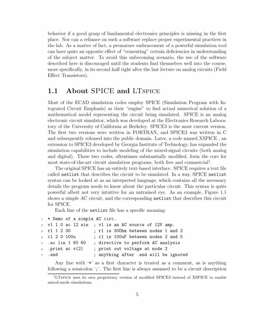
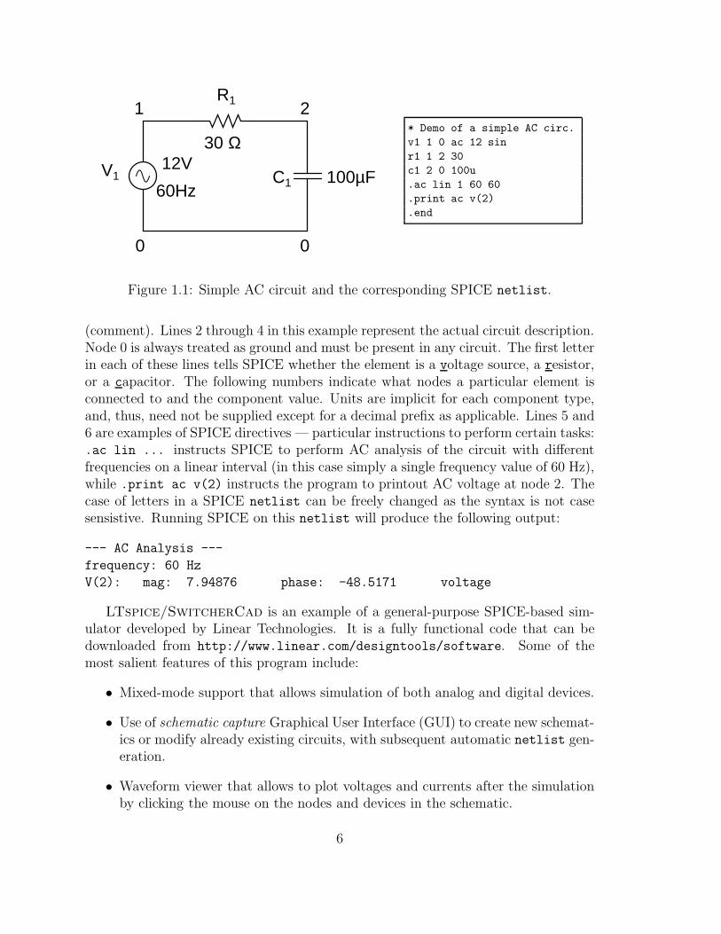
syntax can be looked at as an interpreted language, which contains all the necessarydetails the program needs to know about the particular circuit. This syntax is quitepowerful albeit not very intuitive for an untrained eye. As an example, Figure 1.1shows a simple AC circuit, and the corresponding netlist that describes this circuitfor SPICE.
Each line of the netlist file has a specific meaning:
1 * Demo of a simple AC circ.
2 v1 1 0 ac 12 sin ; v1 is an AC source of 12V amp.
3 r1 1 2 30 ; r1 is 30Ohm between nodes 1 and 2
4 c1 2 0 100u ; c1 is 100uF between nodes 2 and 0
5 .ac lin 1 60 60 ; directive to perform AC analysis
6 .print ac v(2) ; print out voltage at node 2
7 .end ; anything after .end will be ignored
Any line with ‘*’ as a first character is treated as a comment, as is anythingfollowing a semicolon ‘;’. The first line is always assumed to be a circuit description
1LTspice uses its own proprietary version of modified SPICE3 instead of XSPICE to enable
mixed-mode simulations.
5
C1 100µF
30 Ω
R1
V112V
60Hz
0 0
21* Demo of a simple AC circ.
v1 1 0 ac 12 sin
r1 1 2 30
c1 2 0 100u
.ac lin 1 60 60
.print ac v(2)
.end
Figure 1.1: Simple AC circuit and the corresponding SPICE netlist.
(comment). Lines 2 through 4 in this example represent the actual circuit description.Node 0 is always treated as ground and must be present in any circuit. The first letterin each of these lines tells SPICE whether the element is a voltage source, a resistor,or a capacitor. The following numbers indicate what nodes a particular element isconnected to and the component value. Units are implicit for each component type,and, thus, need not be supplied except for a decimal prefix as applicable. Lines 5 and6 are examples of SPICE directives — particular instructions to perform certain tasks:.ac lin ... instructs SPICE to perform AC analysis of the circuit with differentfrequencies on a linear interval (in this case simply a single frequency value of 60 Hz),while .print ac v(2) instructs the program to printout AC voltage at node 2. Thecase of letters in a SPICE netlist can be freely changed as the syntax is not casesensistive. Running SPICE on this netlist will produce the following output:
--- AC Analysis ---
frequency: 60 Hz
V(2): mag: 7.94876 phase: -48.5171 voltage
LTspice/SwitcherCad is an example of a general-purpose SPICE-based sim-ulator developed by Linear Technologies. It is a fully functional code that can bedownloaded from http://www.linear.com/designtools/software. Some of themost salient features of this program include:
• Mixed-mode support that allows simulation of both analog and digital devices.
• Use of schematic capture Graphical User Interface (GUI) to create new schemat-ics or modify already existing circuits, with subsequent automatic netlist gen-eration.
• Waveform viewer that allows to plot voltages and currents after the simulationby clicking the mouse on the nodes and devices in the schematic.
6
• It includes an extensive library of Linear Technology devices. Additional devicescan also be added or constructed with some knowledge of electronics and SPICElanguage. A large collection of device components, digital ICs in particular, isavailable from the user community [1].
• It is one of the most widely used circuit simulators at this time. Many profes-sionals consider it to be superior to some commercial simulators.
• It’s totally free!
The program is distributed for MS Windows operating system only. However,LTspice can be successfully run on Linux and Mac OS X computers with WINEpackage installed [2].
1.2 Getting Started with LTspice
We will start introducing basic functionality of LTspice by building and analyz-ing several simple circuits. The program’s help and example files contain plenty ofadditional interesting information.
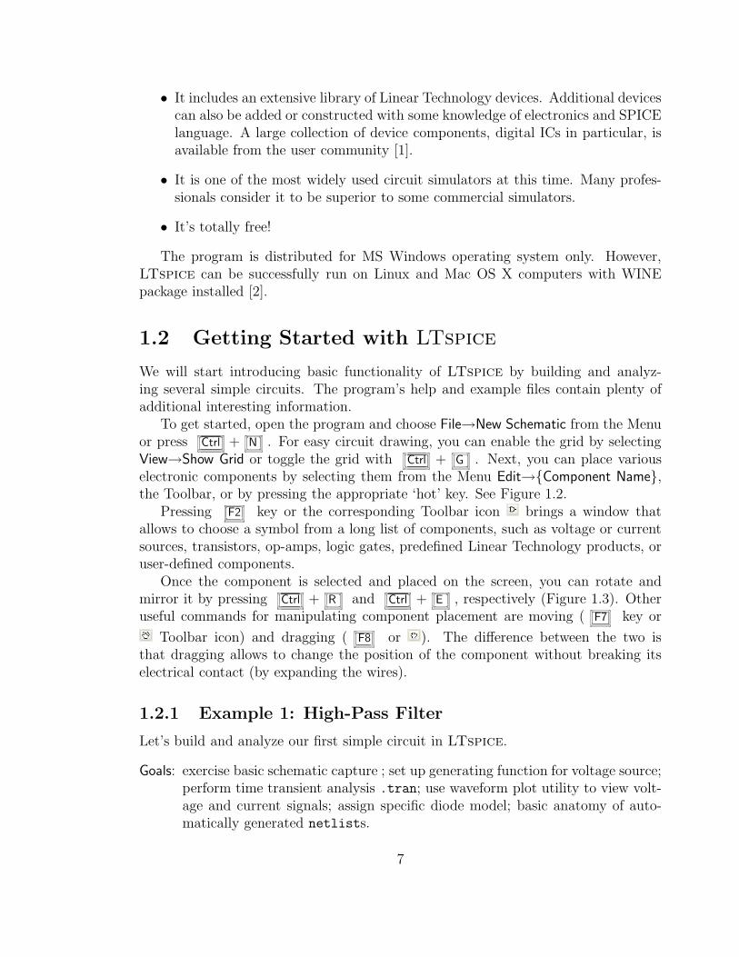
To get started, open the program and choose File→New Schematic from the Menuor press Ctrl + N . For easy circuit drawing, you can enable the grid by selectingView→Show Grid or toggle the grid with Ctrl + G . Next, you can place variouselectronic components by selecting them from the Menu Edit→Component Name,the Toolbar, or by pressing the appropriate ‘hot’ key. See Figure 1.2.
Pressing F2 key or the corresponding Toolbar icon brings a window thatallows to choose a symbol from a long list of components, such as voltage or currentsources, transistors, op-amps, logic gates, predefined Linear Technology products, oruser-defined components.
Once the component is selected and placed on the screen, you can rotate andmirror it by pressing Ctrl + R and Ctrl + E , respectively (Figure 1.3). Otheruseful commands for manipulating component placement are moving ( F7 key or
Toolbar icon) and dragging ( F8 or ). The difference between the two isthat dragging allows to change the position of the component without breaking itselectrical contact (by expanding the wires).
1.2.1 Example 1: High-Pass Filter
Let’s build and analyze our first simple circuit in LTspice.
Goals: exercise basic schematic capture ; set up generating function for voltage source;perform time transient analysis .tran; use waveform plot utility to view volt-age and current signals; assign specific diode model; basic anatomy of auto-matically generated netlists.
7
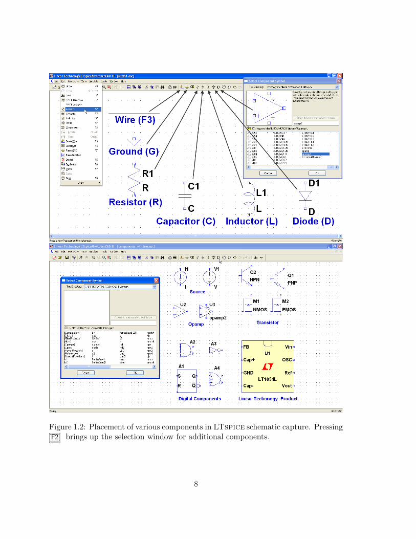
Figure 1.2: Placement of various components in LTspice schematic capture. PressingF2 brings up the selection window for additional components.
8

Figure 1.3: Orientation options prior to the component’s placement.
First, create a circuit shown in Figure 1.4 and assign appropriate values to the ca-pacitor and the resistor. You can find a voltage source symbol (called voltage) inthe list of components after pressing F2 key. To edit component properties, place
the cursor on top of the element so that it is transformed into a hand shape andthen right-click with the mouse.
Figure 1.4: Assigning component values.
SPICE automatically assumes appropriate SI units for all of its component values.The prefix for the unit can be specified as follows:
T = Terra = 1012 K = Kilo = 103 N = nano = 10−9
G = Giga = 109 M = milli = 10−3 P = pico = 10−12
MEG = Mega = 106 U = micro = 10−6 F = femto = 10−15
For example, if you want a 10KΩ resistor, simply type 10K for the resistance value.Note: SPICE commands are not case sensitive. For example, 10M typed in for a
resistance value is the same as 10m, which is 10mΩ (10 milliohm)! If what you reallyintended was 10 MΩ, you should use 10MEG (or 10meg) instead.
9

For now, enter 10K for resistance and 0.01u for capacitance. Note that the valueof the components will appear where previously there were letters R and C. You canalso right-click on these letters to open up a simpler version of the component valueeditor window, which too can be used to specify the component value. Letters R1,C1 and V1 are the name of the elements that SPICE uses in their reference. Youcan right-click and change them to whatever you want as long as these names remainunique.
Next, let’s specify the voltage source. LTspice allows to assign various generatingfunctions to its voltage and current sources, including DC, sinusoidal AC, exponential,triangular, square forms, etc. It even allows to load arbitrarily complex waveformsfrom .wav files (more on that later). For now, right-click on the voltage source. Whenyou do so for the first time, it brings up a simple window that allows to specify a DCsource voltage and its series resistance. For other options click on Advanced button,which will bring another window with more options. To specify a time-dependantvoltage source outputting repetitive pulses of square, triangle, sawtooth, etc. shape,it is convenient to use PULSE option. After selecting this option, enter the values asshown in Figure 1.5. This will produce a square-wave with a 1kHz repetition ratewith high and low voltage values of ±5 V. Leaving Ncycles entry blank means thepulse will be repeating endlessly for the whole duration of the simulation. Most of theentries are self-explanatory. One precautionary remark relates to Trise and Tfall
entries. Setting Trise = Tfall = 0 or leaving these entries blank will lead to adefault behavior where LTspice will use a value of 10% of Ton or Toff, whichever issmaller, for the rise and fall times. While a convenient choice for the default behavior,it may be confusing to the user who explicitly supplied 0 to these entries expectingto get a sharp edge. Instead, for a sharp edge, one should supply a sufficiently smallbut nonzero value. In this example, we specify Trise = Tfall = 1n for 1ns rise andfall times. Press OK button. The specified PULSE options should now appear next tothe voltage source symbol.
LTspice has six different types of analyses: time-transient, small signal AC, DCoperating point (Q-point), DC source sweep, small signal DC transfer function, andintrinsic noise analysis. We will go over the first 3 in this tutorial using variousexamples.
To do time-transient analysis click Simulate→Edit Simulation Cmd. Select Transienttab, and enter 5m for Stop Time, then press OK. See Figure 1.6. This will produce atext line .tran 5m, a SPICE directive — a command with additional instructions forthe simulator. In this particular case, it instructs LTspice to perform time-transientanalysis of the circuit for 5ms. Place the command anywhere in your schematic. Whenyou become familiar with SPICE netlist syntax, you can insert SPICE directivesdirectly by pushing icon on the Toolbar or pressing S key. Once the appropriatestring is created, just place it anywhere in your schematic.
There are many SPICE directives performing various functionalities during orafter the simulation. Some of them will be introduced in this tutorial. Refer to the
10

Figure 1.5: Assigning square wave to the voltage source.
program’s help files for a full description of the syntax for possible directives (alsoknown as dot commands). Alternatively, you can specify the string to be treated ascomment — this can be used to disable certain commands, or to add descriptive textto your circuit. Another way to add such text comments is by pressing T key or
icon on the Toolbar, and then placing the string in your schematic. Such stringshave no effect on simulations.
SPICE directive .tran contains several useful entries. In particular, Time to
Start Saving Data can be used to ignore time-transients of the circuit by specifyingappropriate waiting time. This is commonly done when one is only interested in asteady-state behavior of the circuit.
Click on Run icon or select Simulate→Run from the Menu bar. If the simulationhas successfully finished, a new window will appear where you can display simulationresults. Additionally, LTspice writes several files to the disk. A text file with exten-sion .log contains messages pertaining to the simulation status with any warnings orerrors. Another text file .net is the automatically generated netlist of the circuit.Finally, a binary file with extension .raw contains the actual results of the simulationsuch as voltages for all nodes, etc. You can choose to have LTspice automaticallydelete these temporary files after the program exit by going to the Control Panel(Tools→Control Panel) and then selecting Operation tab.
To measure the voltage on the resistor, click at the wire above it when the cursorchanges its shape to a red probe . This voltage measurement is relative to theground. The lower-left corner of the main window displays interactive messages aboutthe position of the cursor and description of the action to be taken upon clicking. SeeFigure 1.7.
11

Figure 1.6: Setting up time-transient analysis.
LTspice waveform plotting utility is very flexible and you should spend sometime familiarizing yourself with its many options. Some of the most commonly usedoperations are listed below.
• To measure voltage across two different nodes, hold the left mouse button point-ing the cursor at the position of the first node. The probe will “detach” andstay at that location. Drag the probe to the other node until it turns black
. Release the button for the measurement.
• To measure current flowing through a component simply place the cursor overit. The probe will change its shape into a current probe . To force for acurrent measurement in a location of a connecting wire, hold down Alt key,then click to plot the current.
• To measure power dissipated in an element, click on it while holding down Alt
key. The probe should transform into a thermometer-like shape .
• Various zooming options are available in the plot window. Simply select theregion of interest to zoom in. Ctrl + E returns the display to its defaultview.
• Selecting new signals will add the corresponding waveforms to the same plotpane. Selecting the same trace twice, removes all other traces from that pane.
• Add or remove additional plot panes from Plot Settings Menu bar or by right-clicking on the plot window.
12
Figure 1.7: Use of plotting utility to view the simulation results.
• Edit mathematical expression being plotted, or plot one signal vs. another. Forexample, V(N001,N002)*I(C1) plots the voltage between nodes N001 and N002
times the current flowing through C1 (the dissipated power). V(N002)-V(N001)plots the voltage difference between the two nodes, as does V(N002,N001). Referto Waveform Arithmetic in LTspice help files for full description. The low-leftcorner of the main window displays the node number when the cursor is placedover a particular area in the circuit.
• Change axes to display data either on linear or logarithmic scale.
• Use up to two cursors on each trace to read out abscissa and ordinate values atlocations of interest in the plot, such as corner points. These cursors functionin a similar manner as with conventional oscilloscope.
• Find the average, rms, or the integrated values of a trace. Figure 1.8 shows anexample of how to use cursors and perform trace integration.
• Fast Fourier Transform (FFT).
As a matter of exercise, create two plot panes. Use them to display power de-posited in the resistor as a function of time in one pane, and power deposited inthe capacitor in the other pane. Find the average values for dissipated power in thetwo elements. Does the average value for power dissipated in the capacitor agreewith your expectations? After that, keeping only one pane, plot voltage across thecapacitor vs. the current flowing through it. What is the shape of this trace?
Next, modify the circuit by including a diode in parallel with the resistor. Right-click on the diode, then click on Pick New Diode button. This will bring a list of
13

Figure 1.8: Use of cursors and trace integration in the plotting utility.
Figure 1.9: Adding 1N914 diode to the circuit.
diode models available in LTspice library. Select 1N914 diode. See Figure 1.9.Rerun the simulation and plot the voltage across the resistor. Do you see what youhave expected?
By selecting View→SPICE Netlist , you can bring up netlist for the circuit youhave built. This netlist can be used in other SPICE-based programs, or specialutility programs, such as printed circuit board design tools [3]. The netlist for yourcircuit should look something like:
14
1 * Path to where you saved .asc (LTspice) file of the circuit
2 R1 N002 0 10K
3 C1 N001 N002 0.01
4 V1 N001 0 PULSE(-5 5 0 1n 1n 0.5m 1m)
5 D1 0 N002 1N914
6 .model D D
7 .lib C:\Program Files\LTC\SwCADIII\lib\cmp\standard.dio
8 .tran 5m
9 .backanno
10 .end
The meaning of most of the lines can be recognized in the light of what we have alreadyseen. The diode on line 5 has 1N914 in place of its value. Line 6 informs SPICEthat a particular diode model should be used (in this trivial form, this command isredundant and can be removed), whereas the actual parameters for 1N914 diode arecontained in the library file specified using the .lib directive on line 7. Line 9 is anLTspice-specific command inserted in every automatically generated netlist anddoes not affect the actual simulation flow (it is only used in postprocessing with theplotting utility).
1.2.2 Example 2: Simplistic Op-Amp
Here we will use a simple op-amp example (Problem 6.3 from the Lab Manual) todemonstrate other capabilities of LTspice.
Goals: use of Net Labels; quiescent point analysis using .op directive; use of param-eters (.param directive); stepping a parameter value (.step directive); usingmeasurement command .meas; small gain AC analysis using .ac directive.
To get started, draw the circuit as shown in the Lab Manual. For transistorschoose two pnp and one npn symbols from the list of components. You will have torotate or mirror the symbols for their optimal placement. Selecting a specific modelfor transistors is done in the same way as assigning a model for diodes — right-clickon the transistor, press Pick New Transistor, then choose 2N3906 for PNP and 2N3904for NPN. Specify values for all of the components. Also, rename the components tofollow the schematic. See Figure 1.10 for what your circuit should look like at thisstage.
Next, use a feature called Label Net to rename the nodes from their default names,as shown in Figure 1.11. Node relabeling is done by pressing either F4 or the
Toolbar icon , typing a new name, and then attaching it to the circuit. Each nodeis then referred by its (new) name, which must be unique for the circuit. If twoor more identical net names are present, SPICE considers them to be electricallyconnected (even if there is no wire present in the schematic capture). This feature is
15

Figure 1.10: Creating a simple op-amp circuit.
particularly convenient to use in a circuit with many interconnections to avoid clutterin the schematic. Here we will use this feature to “attach” voltage sources: two DC(±15V) and two SINE sources. A sinusoidal voltage sources can be created in analogyto PULSE source of the previous example. Here they are given amplitudes of 100mVand 95mV for inverting and non-inverting inputs of the differential amplifier, Va andVb respectively. The frequency is set to 1kHz.
Q-point analysis
SPICE directive .op can be used to perform Q-point analysis. It computes the DC op-erating point treating capacitances as open circuits and inductances as short circuits.This command is run implicitly by SPICE prior to performing other types of analysessuch as small-signal AC gain calculations. We will invoke this command explicitly todetermine Q-point of this circuit. SINE voltage sources assume their DC offset valuesfor the Q-point analysis, which are zero in our case for Va and Vb sources. Create andplace .op command in the circuit either by selecting Simulate→Edit Simulation Cmdfrom the Menu bar and then going to DC op pnt tab or typing it in directly afterpressing S key. Completed circuit ready for simulation is shown in Figure 1.11.
Let’s briefly examine netlist by going to View→SPICE Netlist Menu. It shouldlook like the following (comments added manually). Note the use of new node namesin the description of the circuit.
* Path to the saved .asc (LTspice) file with the circuit
V1 VEE 0 15 ;;;;;;;;;;;;;;;;;;;;;;;
V2 VCC 0 -15 ; circuit description ;
16

Figure 1.11: Circuit with renamed nodes and .op SPICE directive added.
Q1 VCC Va VE12 0 2N3906 ; Q for a BJT ;
Q2 VC2 Vb VE12 0 2N3906 ; ;
RC2 VC2 VCC 2.7K ; ;
RE12 VEE VE12 2.7K ; ;
V3 Va 0 SINE(0 100m 1k) ; ;
Q3 Vout VC2 VE3 0 2N3904 ; ;
RE3 VE3 VCC 1K ; ;
RC3 VEE Vout 2.27K ; ;
V4 Vb 0 SINE(0 95m 1k) ;;;;;;;;;;;;;;;;;;;;;;;
.model NPN NPN ;;;;;;;;;;;;;;;;;;;;
.model PNP PNP ; SPICE directives ;
.lib C:\PROGRA~1\LTC\SwCADIII\lib\cmp\standard.bjt
.op ; ;
.backanno ; ;
.end ;;;;;;;;;;;;;;;;;;;;
Running simulation of this example brings up a window with Q-point values of allvoltages and currents:
--- Operating Point ---
17

V(vee): 15 voltage
V(vcc): -15 voltage
...
Ic(Q3): 0.00614037 device_current
Ib(Q3): 1.90069e-005 device_current
Ie(Q3): -0.00615938 device_current
...
You can access these values after closing the window by pointing the cursor to thecircuit. A short description and the calculated value will appear in the lower-leftcorner of the main window. Pointing to various components also reports dissipatedpower for the DC operating point.
It is possible to replace any of the component values with a named variable — aparameter — which can be assigned a numerical value elsewhere. For example, right-click on RC3 resistance value, 2.27K, and type-in a variable name in curly bracesRC3val in its place. Next, create a SPICE directive.param Rval 2.27K
(without curly braces!) and rerun the simulation. You should get the same result asbefore.
Note that the Q-point for V(Vout) is offset from zero. You can change RC3val
to bring it closer to zero, which would be more along the lines of a desired op-ampbehavior. In a real-life implementation of this circuit, such details will depend on theactual transistors used, which can differ significantly from their typical specificationsused by the program. There is a way to scan a parameter using .step directive.Create a SPICE command.step param RC3val 2.2K 2.7K 10
and place it somewhere in the schematic. This command instructs the program torepeat calculation while scanning the parameter RC3val from 2.2kΩ to 2.7kΩ witha step of 10Ω. Refer to LTspice help files for additional information about .step
command syntax. Run the example again, then click on Vout node to plot Q-pointvoltage as a function of the scanned parameter. What value of RC3 produces V(Vout)= 0? You can find the relevant RC3val value with a help of a trace cursor in theplotting utility by clicking on the legend. Another way to determine the RC3 valueis through a powerful .meas[ure] command. We will gradually introduce some ofits functionalities. Refer to LTspice help for a complete description. This commandallows to evaluate a user-defined quantity derived from the results of simulations.Create the following SPICE directive:.meas op RC3ideal find RC3val when V(Vout)=0
and place it on your schematic. This command instructs SPICE to find RC3val valuewhen V(Vout)=0 and label the result RC3ideal. The second (optional) word “op” inthis command specifies which type of analysis .meas was applied to (e.g., it wouldbe .tran for time-transient analysis). By now all of your SPICE directives (an exact
18

order is irrelevant) should look like:.op
.step param RC3val 2.2K 2.7K 10
.meas op RC3ideal find RC3val when V(Vout)=0
Run the simulation again. Choose View→SPICE Error Log from the Menu bar. Finda string in the log file that looks like this:rc3ideal: rc3val=actual value at ...
and substitute this value for RC3 resistance. Run the example again using .op
command (remove or comment out all other directives) to verify that indeed Vout = 0as expected.
Save this circuit to simple_opamp.asc file for future work.
Small-signal AC gain
Here we will determine a small-signal AC gain of the simple op-amp using severaldifferent methods. First, let’s calculate AC gain using time-transient analysis. Sim-ulate the circuit for 10ms by including .tran 10m command. Next, create two plotpanes and display the input signal vdiff = Vb − Va on one and Vout on the other, seeFigure 1.12. Activate two trace cursors for each of the plot, and “measure” peak-to-peak voltage (the difference between the cursors) for each case. Find the AC gainG = ∆Vout/∆vdiff .
Figure 1.12: Displaying results of time-transient analysis in two plot panes.
Another way to extract this information is to use .meas commands. The followingthree lines achieve the desired result.
1 .meas tran Vout_pp pp V(Vout)
2 .meas tran vdiff_pp pp V(vb)-V(va)
19

3 .meas tran G param Vout_pp/vdiff_pp
Line 1 finds the peak-to-peak (pp keyword) value of Vout and labels the resultVout_pp. Other possible keywords are avg (average), max, min, rms, and integ
(integrate the expression following it). Line 2 does a similar thing for Vb − Va. Thelast line performs some basic arithmetic on parameters Vout_pp and vdiff_pp andstores the result in variable G. Run the simulation with these 3 lines included asSPICE directives and view the computed value of G in the .log file. Compare theresult to the previously calculated value.
A dedicated SPICE command to calculate small-signal AC gain is .ac. ChooseSimulate→Edit Simulation Cmd, then select AC Analysis tab. Select Decade for a typeof sweep, with 10 points per decade starting from 1Hz to 50MHz. This type ofanalysis requires an AC stimulus — a voltage source that will be “driven” at differentfrequencies. For example, to turn Va source into an AC stimulus, bring up its voltagesource window, and type in 1 into the AC Amplitude field. A label AC 1 will appearnear the voltage source. Now you can run the simulation and display Bode plot ofthe gain vs. frequency by clicking on Vout node. See Figure 1.13. A solid line showsthe magnitude, and a dashed line the phase. By clicking on the magnitude axis youcan choose for the gain to be displayed on a linear or logarithmic scale. By clickingon the phase axis, you can choose to alternatively plot group delay (a measure of thetransit time of a signal through the device) associated with the complex gain. Note180 phase at low frequencies, which indicates Va to be an inverting input. Comparethe gain at 1kHz with what you have found above using time-transient analysis.
Figure 1.13: Setting up .ac analysis of the circuit.
20
1.2.3 Example 3: Using External Models
Here we will consider 3 short examples: a voltage follower, an astable multivibrator,and a ring oscillator. In these examples we will explore how to incorporate externalmodels (not part of LTspice) into your simulations.
Goals: assign manufacturer’s SPICE model to op-amp; introduce .subckt directive;set initial conditions with .ic directive; use of .lib and .include statements.
Stability Of Voltage Follower
In this example, we will investigate the stability of a voltage follower built withLM741 op-amp. LM741 is not a Linear Technology product and does not come withLTspice library, but this and similar models can be easily added to your circuits.Go to http://www.national.com and search for “LM741 model” (or search on theInternet for “LM741 SPICE model”). There, you will find a file called LM741.MOD.This model file is available on your lab computer in SPICE\external_components
directory. Download or copy the file to your local directory where you save yourLTspice examples.
LM741.MOD is a SPICE model for LM741 op-amp distributed by its manufacturer,National Semiconductor. Most manufacturers provide SPICE models of many of theirproducts, which can be used in LTspice simulations. LM741.MOD header contains thefollowing:*//////////////////////////////////////////////////////////////////////
* (C) National Semiconductor, Inc.
* Models developed and under copyright by:
* National Semiconductor, Inc.
*/////////////////////////////////////////////////////////////////////
* Legal Notice: This material is intended for free software support.
* The file may be copied, and distributed; however, reselling the
* material is illegal
*////////////////////////////////////////////////////////////////////
* For ordering or technical information on these models, contact:
* National Semiconductor’s Customer Response Center
* 7:00 A.M.--7:00 P.M. U.S. Central Time
* (800) 272-9959
* For Applications support, contact the Internet address:
*//////////////////////////////////////////////////////////
*LM741 OPERATIONAL AMPLIFIER MACRO-MODEL
*//////////////////////////////////////////////////////////
*
* connections: non-inverting input
* | inverting input
* | | positive power supply
* | | | negative power supply
* | | | | output
* | | | | |
* | | | | |
.SUBCKT LM741/NS 1 2 99 50 28
...
21

.SUBCKT command starts a description of the actual model. This directive can beused as an aid in defining a circuit through inclusion of repetitive circuitry containedin a subcircuit definition. Before the simulation runs, the circuit is expanded to a flatnetlist by replacing each invocation of a subcircuit with the circuit elements in thesubcircuit definition. The end of a subcircuit definition must be a .ends directive.
Create a circuit of the voltage follower driving a capacitive load C1. Use genericopamp2 symbol found in the component selection window, see Figure 1.14. “Power”the op-amp with ±15V voltage supplies. Then setup a square-wave voltage sourcewith ±1V amplitude and 1kHz frequency and connect it to the voltage follower. Uselabels as shown in Figure 1.14. To study the behavior of the output for different C1capacitance values, use parameter C in place of its capacitance. Save this circuit tothe same directory as LM741.MOD file.
Figure 1.14: Voltage follower circuit.
Symbol opamp2 does not have any model associated with it and this circuit willnot work as is. To use LM741/NS with this symbol you must perform two steps. 1)Right-click on the op-amp to open Component Attribute Editor window, and modifyAttribute Value so that is reads LM741/NS. This string should match the name of thesubcircuit found on .SUBCKT line in the LM741.MOD file. 2) Add .include LM741.MOD
command to your circuit. This directive includes the named file as if that file had beentyped into the netlist in place of the .include command. An absolute path namemay be entered for the filename. If a relative path is provided, LTspice looks first inthe directory <SwCADIII>\lib\sub and then in the directory that contains the callingnetlist (the local directory). <SwCADIII> is the directory containing the scad3.exe
22

Figure 1.15: Setting up LM741 op-amp.
(LTspice) executable, typically installed in C:\Program Files\LTC\SwCADIII. Adda time-transient analysis command, and a command for stepping parameter C so thatthe directives included to your schematic read (see Figure 1.15):.tran 2m
.step param C list 50p 1n 20n
.include LM741.MOD
The second line instructs parameter C to adopt its values from a list of arbitraryvalues following list keyword (here 50pF, 1nF, and 20nF).
Figure 1.16: Viewing the output of the voltage follower.
Run the simulation and plot V(out). Zoom in on the rising or falling edge of thepulse. See Figure 1.16. The ringing that can be seen indicates that the circuit ismarginally unstable. The circuit is more unstable with the larger capacitor due to
23

a smaller phase and gain margins of the loop gain. A problem at the end of Part 1asks you to find phase and gain margins for different capacitor values through .ac
calculations of the loop gain of the circuit. When using .step command, the plottingutility displays all traces corresponding to all steps of the parameter. You can alsochoose to include specific steps in the graph by right-clicking in the plot window andchoosing Select Steps from the Menu.
Save this circuit to voltage_follower.asc file for future work.
Astable Multivibrator
You can simulate circuits in LTspice without explicit voltage sources such as anastable multivibrator. There may be a problem with starting oscillations in a circuitthat employs positive feedback, which we will demonstrate now. Build an astablemultivibrator using LM741 op-amp and perform time-transient analysis for 10ms.See Figure 1.17. As you can see from V(out) output, the oscillations do not startuntil after 5ms into the simulation. As you recall, a positive feedback circuit may havean unstable equilibrium point where all voltages are zero so that in an idealistic case(e.g., in simulations where voltages may be exactly zero, with no input offset voltagein the op-amp, etc.) the self-induced oscillations may take considerable time to start,or may never start at all. To resolve this issue, you can include .ic statement to yourcircuit:.ic V(inv)=1m
This statement specifies initial conditions for time-transient analysis. It sets theinitial voltage on the inverting input of the op-amp to be 1mV. Add this statementand rerun the example. Observe how the output has changed.
Save this circuit to multivibrator.asc file for future work.
Ring Oscillator
You can also build a multivibrator using digital components. Digital circuitry isintroduced in the second half of the course. Here, you will learn how to build asimple ring oscillator using NOT gates, and in particular how to include integratedcircuit models that are not part of LTspice for a later use in the course. Very briefly:digital gates are devices that operate on two-state voltage signals, for example 0Vand 5V (voltages need not to be exact). One state will be known as TRUE, and theother one as FALSE. An inverter (NOT) gate is the simplest digital component withonly one input and one output that inverts the digital signal supplied to its input.It performs a Boolean logic operation known as negation. Its symbol is usuallydrawn as a triangle (buffer) with an inverting circle (bubble).
Next, consider a circuit in which the output of a NOT gate is connected to itsinput. Such a configuration would be meaningless for an ideal NOT gate, becausethe operation of negation can never be satisfied in such a case. In reality, all gateshave a finite propagation delay, which can be defined as a time period starting from
24

Figure 1.17: Astable multivibrator circuit (on the left) that displays a delay in startingthe oscillations (on the right).
when the input to a logic gate becomes stable and valid to when the output of thatlogic gate is stable and valid (“valid” here means that it is one of the two possiblevoltage levels, TRUE or FALSE). For example, 74HCT04 NOT gate from Phillips isspecified to have a typical propagation delay of 10ns under usual operating conditions.Connecting the gate’s output to its input will lead to oscillations between the twovoltage levels (FALSE and TRUE), with a period equal to twice the propagationdelay — about 20ns or 50MHz. A similar situation occurs when any odd number ofNOT gates are connected together, except the period of oscillations becomes longerby the number of gates being used. This configuration is known as ring oscillator.
You can find a selection of digital components for LTspice in the directorySPICE\external_components on your laboratory computer. These files are alsoavailable from the course web-site. Copy 74HCT.LIB file containing SPICE mod-els of various gates from this digital family (found in Digital_74HCTxxx directory)and a NOT gate circuit symbol 74hct04.asy (found in Digital_74HCTxxx\74HCT)to your local directory. Create a new schematic in LTspice and save the file asring_oscillator.asc to the same directory as the other files. Next, insert the in-verter gate symbol in your schematic by bringing up Select Component Symbol window(press F2 ), and changing Top Directory to your local directory. See Figure 1.18. Touse the component you also need to include the library file using .lib 74HCT.LIB or.include 74HCT.LIB directive. The difference between .lib and .include is thatthe former inserts the contents of the file only between .subckt and ends commands,while ignoring other parts of the file. This command is convenient when you want toreuse model definitions from another circuit file or netlist, without including the
25

Figure 1.18: Oscillator ring using 5 inverter gates 74HCT04.
entire circuit. Build the circuit as shown in Figure 1.18 and perform time-transientanalysis for 1µs. If you do not include the initial condition statement .ic V(out)=5,the circuit will be simulated incorrectly. In particular, the frequency of oscillationswill be the same as if only a single inverter gate were present, whereas a real-life ver-
sion of this circuit would tend to produce a frequency ×5 lower. A closer look at thecircuit reveals that all 5 NOT gates are performing oscillations in a perfect unison —a scenario possible only in the ideal world of simulations! Real-life gates have slightlydifferent propagation delays, which precludes such behavior from happening. Theinitial condition statement ensures that such pathological case does not occur in thesimulation.
1.2.4 Example 4: Creating Custom Components
Goals: create custom components and circuit blocks for inclusion in other circuits.
In addition to the library of components in LTspice, models for many differenttypes of analog and digital devices may be found on the Internet [4]. Nevertheless, oc-casionally one needs to create a custom component because a particular device model
26

has not been implemented. This ability is also useful for a hierarchical organizationof large circuits — it may be convenient to create a new component that representsa block (a subcircuit), which either repeats several times in the circuit or representsa unit with a well-pronounced functionality. Schematics organized in such a fashionfacilitate their reading and understanding.
Figure 1.19: Steps to creating a custom symbol.
Custom Component Symbol
To create a new component, one needs a circuit symbol and a SPICE model (netlist)of a device or a circuit block. In this example, we will go through these steps. First,you have to draw the component’s symbol that will be used in LTspice schematiccapture or, alternatively, you can reuse an already existing one. To begin from scratch,select File→New Symbol from the pull-down Menu. Once the program is in the symbolediting mode, an additional Draw Menu provides options to draw a line, rectangle,circle, arc, and to add text to your symbol. Draw a simple symbol for an op-amp asshown in Figure 1.19.
Step 1. Create a symbol, as shown in Figure 1.19, consisting of a rectangle and atriangle.
27
Step 2. Select Edit→Add Pin/Port from the Menu to add pins to the symbol in thefollowing order: in+, in-, V+, V-, and out.
Step 3. Select Edit→Attributes→Attribute Window from the Menu. Select InstName
attribute to add to the schematic. It will display the actual value of theattribute in your schematic. Repeat this step for Value attribute.
Step 4. Select Edit→Attributes→Edit Attributes and enter X for Prefix, myopamp forValue, and some description message such as ‘alternative op-amp symbol’ forDescription.
The most important attribute is called Prefix. It determines the basic type ofa symbol. If the symbol is intended to represent a SPICE primitive, the symbolshould have an appropriate prefix: R for resistor, C or capacitor, M for MOSFET,etc. The prefix should be X if you want to use the symbol to represent a subcircuitthat incorporates an external netlist model (e.g. LM741). The rectangle in yourschematic will be changed to a filled shape.
The next significant attribute is Value. As you recall from the LM741 example,it should match the string after the .subckt command in the external file. For nowwe set this value to myopamp, but it may have to be replaced with whatever string onthe .subckt command line in the model file to be used with this symbol.
The order of pins is significant — it must match that of the nodes from the.subckt line. The specified order of pins was chosen so that the symbol can be usedwith standard model files for op-amps, such as LM741.MOD. The order of the nodescan be seen from the file content:...
*//////////////////////////////////////////////////////////
*LM741 OPERATIONAL AMPLIFIER MACRO-MODEL
*//////////////////////////////////////////////////////////
*
* connections: non-inverting input
* | inverting input
* | | positive power supply
* | | | negative power supply
* | | | | output
* | | | | |
* | | | | |
.SUBCKT LM741/NS 1 2 99 50 28
...
Double-check that the order of the pins in your symbol matches the order found inLM741.MOD file by bringing up View→Pin Table from the Menu. See Figure 1.20. Savethe symbol to myopamp.asy file.
Because this symbol is pin-compatible with the other op-amp symbol opamp2 youhave been using, you can use these two symbols interchangeably (for example, withLM741.MOD file). To use the new symbol, make sure myopamp.asy file is placed inthe same directory as your .asc schematic file. Bring up Select Component Symbolwindow and change Top Directory to your local directory. You should see the newsymbol in the window available for insertion into your schematic.
28

Figure 1.20: Attributes and correct pin order for the op-amp symbol.
1 * Path to the saved .asc (LTspice) file with the circuit
2 V1 VEE 0 15
3 V2 VCC 0 -15
4 Q1 VCC Va VE12 0 2N3906
5 Q2 VC2 Vb VE12 0 2N3906
6 RC2 VC2 VCC 2.7K
7 RE12 VEE VE12 2.7K
8 V3 Va 0 SINE(0 100m 1k)
9 Q3 Vout VC2 VE3 0 2N3904
10 RE3 VE3 VCC 1K
11 RC3 VEE Vout 2.27K
12 V4 Vb 0 SINE(0 95m 1k)
13 .model NPN NPN
14 .model PNP PNP
15 .lib C:\PROGRA~1\LTC\SwCADIII\lib\cmp\standard.bjt
16 .op
17 .backanno
18 .end
Figure 1.21: Raw SPICE file automatically generated for the three-transistor op-amp..
Custom SPICE Model
Next, we will create an external SPICE model containing the simple op-amp fromthe earlier Example 2. Generally, creating a new model requires knowledge of SPICE
29
* myopamp.txt: model for a three-transistor op-amp
.SUBCKT myopamp Vb Va VEE VCC Vout
Q1 VCC Va VE12 0 2N3906
Q2 VC2 Vb VE12 0 2N3906
RC2 VC2 VCC 2.7K
RE12 VEE VE12 2.7K
Q3 Vout VC2 VE3 0 2N3904
RE3 VE3 VCC 1K
RC3 VEE Vout 2.27K
.model NPN NPN
.model PNP PNP
.lib C:\PROGRA~1\LTC\SwCADIII\lib\cmp\standard.bjt
.backanno
.ends
Figure 1.22: Contents of myopamp.txt SPICE model file.
language. However, with LTspice automatically creating netlists, this job largelyamounts to copying and pasting.
Open the file simple_opamp.asc, which you saved earlier. Copy the contents ofSPICE netlist (from View→SPICE Netlist Menu) and paste it into a text editor (e.g.,Notepad). See Figure 1.21. Examine the file. It may be slightly different than whatis shown in Figure 1.21. Note that lines 2, 3, 8 and 12 contain definitions for voltagesources, and that line 16 contains a SPICE directive for circuit analysis. Delete theselines as they do not belong in the subcircuit body. Next, place the following line atthe beginning of the file (after the first comment line):.SUBCKT myopamp Vb Va VEE VCC Vout
and change .end to .ends. Note that the order of the pins must follow that ofthe symbol: non-inverting input, inverting input, positive power supply, negativepower supply, and the output. The modified file should look like what is shown inFigure 1.22.
Save the model file to myopamp.txt. Now you can use this model file along withmyopamp symbol by setting Value to myopamp and adding .include myopamp.txt
statement to your circuit.
Blocks And Hierarchical Organization Of Large Circuits
There exists a convenient way in LTspice to organize large circuits using blocks.Each block is a component symbol (stored in some_name.asy file), which is linkedto a circuit schematic with identical filename except for the file extension (stored insome_name.asc file). Node association is achieved through matching names of pins inthe symbol file and net labels in the schematic file. Right-clicking on such component(also known as block) allows one to open and edit its schematic. While the use ofSPICE models through .include statement fits best when representing an existingdevice or a component, circuit blocks are a convenient way to organize large circuitsunder development, or, when the internal workings of a lower-hierarchy device needto be looked at and possibly tweaked.
30
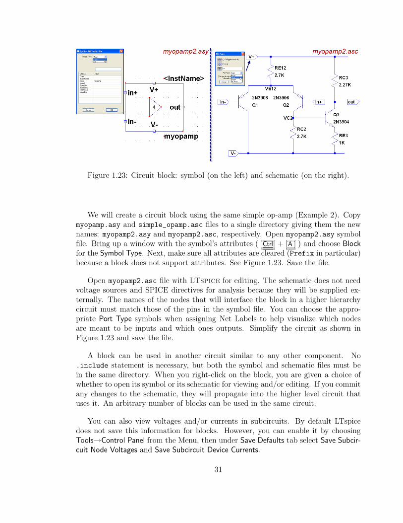
Figure 1.23: Circuit block: symbol (on the left) and schematic (on the right).
We will create a circuit block using the same simple op-amp (Example 2). Copymyopamp.asy and simple_opamp.asc files to a single directory giving them the newnames: myopamp2.asy and myopamp2.asc, respectively. Open myopamp2.asy symbolfile. Bring up a window with the symbol’s attributes ( Ctrl + A ) and choose Blockfor the Symbol Type. Next, make sure all attributes are cleared (Prefix in particular)because a block does not support attributes. See Figure 1.23. Save the file.
Open myopamp2.asc file with LTspice for editing. The schematic does not needvoltage sources and SPICE directives for analysis because they will be supplied ex-ternally. The names of the nodes that will interface the block in a higher hierarchycircuit must match those of the pins in the symbol file. You can choose the appro-priate Port Type symbols when assigning Net Labels to help visualize which nodesare meant to be inputs and which ones outputs. Simplify the circuit as shown inFigure 1.23 and save the file.
A block can be used in another circuit similar to any other component. No.include statement is necessary, but both the symbol and schematic files must bein the same directory. When you right-click on the block, you are given a choice ofwhether to open its symbol or its schematic for viewing and/or editing. If you commitany changes to the schematic, they will propagate into the higher level circuit thatuses it. An arbitrary number of blocks can be used in the same circuit.
You can also view voltages and/or currents in subcircuits. By default LTspicedoes not save this information for blocks. However, you can enable it by choosingTools→Control Panel from the Menu, then under Save Defaults tab select Save Subcir-cuit Node Voltages and Save Subcircuit Device Currents.
31

1.3 Practice Problems
1. Build an astable multivibrator using the SPICE model of the simple three-transistor op-amp and its symbol that you made earlier (with .include state-ment) using ±15V power supply. Print out few cycles of the output. Determinethe peak-to-peak voltage of the output (use .meas directive). Is the outputsymmetric around zero? Explain why.
2. An enhancement n-channel MOSFET can be connected in a diode configuration,see Figure 1.24. Obtain I-V curve of such a “diode” for 2N7000 n-channelenhancement MOSFET scanning the voltage from -0.9 to 12V and print theresult. (Hint: use .op and .step directives). Find the incremental resistancefrom I-V curve at 5V drain-source voltage. What is the dissipated power atthat point? Use 2N7000 SPICE model from the library files available from thecourse web-site. This model requires a 4-input symbol, which can be foundalong with the model file in SPICE\external_components\2N7000 directory.Make sure that SpiceModel attribute of the component is set to 2N7000 andthat the appropriate .include statement is present. The 4th input is usedto specify temperature for SPICE model of this MOSFET. The temperatureinput needs a dummy voltage source whose DC value in volts is interpreted astemperature in C. Set the temperature to be 20C. How does the incrementalresistance at 5V change when the temperature is 80C?
=
Figure 1.24: MOSFET in diode configuration (Problem 2).
3. The stability margin of a voltage follower driving a capacitive load dependson the capacitor’s value. Use LTspice to calculate gain margin and phase
margin — useful criteria of the circuit’s degree of (in)stability — for this cir-cuit for 50pF, 1nF, and 20nF C1 capacitance (voltage_follower.asc file, seeFigure 1.15). Fill out the following table (indicate the units).
32

C f1 = f0dB GL1 φL1 f2 = f−180 GL2 φL2 GM φM f0
50pF 0dB −180
1nF 0dB −180
20nF 0dB −180
Here, f1 = f0dB and f2 = f−180 are the frequencies for which the loop gainGL = 0dB and the loop phase φL = −180, respectively. GM is the gain mar-gin: GM = GL2 − GL1. φM is the phase margin: φM = φL2 − φL1. f0 is thefrequency of oscillations you are observing in time-transient analysis in LTspiceafter a steep rise or fall of the input signal.Note: in one of the earlier examples you have obtained Bode plot of the closed
loop gain of this circuit, but to determine phase and gain margin you should findBode plot of the loop gain. These are two distinct gains. Recall that the loopgain is determined from the signal gain traveling around the loop formed by theop-amp and the negative feedback. To find the loop gain, insert AC stimulus inthe path of the negative feedback, while grounding the input of the voltage fol-lower. See Figure 1.25. The loop gain is given by the expression -V(out)/V(in),which you should plot after running an .ac analysis. Time-transient analysison the original circuit is also necessary to determine the frequency of inducedoscillations, f0.
Figure 1.25: Setup to determine loop gain of the voltage follower driving a capacitor.
4. Figure 1.26 shows a center-tapped transformer implementation in LTspice.Inductor component used for this circuit is ind2, which is found among thepredefined components in LTspice. There are three inductors: L1 correspond-ing to the primary coil, and L2 and L3 corresponding to the secondary coil. NoteSPICE directive K1 L1 L2 L3 1 which defines mutual inductance with couplingcoefficient K1=1. It means that all three coils fully induce each other (an analogto them being wound on an iron core with a very high permeability). The rela-tionship between the voltages for a pair of coils with a coupling coefficient of 1 is|V1/V2| =
√
L1/L2. L1 is specified to be 10H. 5Ω in series with L1 represents theprimary coil resistance (you can also specify this and other parameters by right-clicking on the inductors). Build a full-wave rectifier using this center-tapped
33

Figure 1.26: Center-tapped transformer in LTspice.
transformer that converts 120VAC 60Hz voltage to 10V DC driving 10kΩ loadwith 1% ripple. Show calculations for the component values. Then double-checkyour calculations by observing the output of your rectifier in LTspice. Use1N4007 rectifier diode model found in the files (in SPICE\external_components
directory) available for download from the course web-site. Move 1n4007.txt
file to the same directory as your schematic .asc file. Enter d1n4007 for Valuein the diode’s symbol and add .include 1n4007.txt statement. Finally, de-termine how much power is dissipated on average in all of the diodes.
34
PART 2
Optional Experiments Using LTspice
You will find a shortcut to SPICE directory on your lab computers. This directorycontains symbols and model files for some of the components, which are not availablein LTspice, but are used in the experiments outlined here. It is recommended thatyou create a new directory for each new experiment and copy only needed symboland model files for inclusion into your schematic .asc file saved in the same directory.Please make sure you save your files to your own storage medium between lab sessions — the lab computers have a shared usage and any files you leave on their hard-driveswill be eventually overwritten.
The main directory (SPICE) has two subdirectories: external_components withcomponent definitions, and experiments that contains circuit schematics files for usewith some of the experiments outlined in Part 2. The description for each experimentwill indicate whether additional files from SPICE directory may be needed.
Directory external_components contains an additional folder named dview ordigital view. It contains two “elements” useful for visualizing multiple digital tracesoverlapping in time without having to open a new plot pane each time another signalis being added to the plot. The two symbol files in that folder are dview5.asy anddview10.asy, each allowing up to 5 or 10 traces to be viewed simultaneously. Simplyconnect the nodes you wish to be viewed to dview5 or dview10 inputs and then viewthem by clicking on the corresponding outputs of the “element” with the probe .Each new trace viewed this way will be scaled to fit a single plot pane. As a result,the vertical axis reading does not correspond to the actual voltage of the signal. Touse the digital view “elements”, copy both .asy and dview.lib files to your currentdirectory. Insert the symbol to your circuit and add .include dview.lib SPICEdirective.
35

2.1 Chapter 8 Experiments
InputA
InputB
Output
+5V
P1 P2
N1
N2
Figure 2.1: 2-input CMOS NAND gate.
Exp (LTspice 8.1). 3-input CMOS NAND gate. Figure 2.1 shows a 2-inputcomplimentary metal-oxide-semiconductor (CMOS) NAND gate. It consists of twon-channel MOSFETs, N1 and N2, connected in series, and two p-channel MOSFETs,P1 and P2, connected in parallel. This gate can be expanded to more inputs byappropriately adding additional pairs of complimentary MOSFETs.
Expand this gate to a 3-input NAND and implement it in LTspice. Use defaultMOSFET transistor models associated with symbols nmos and pmos in LTspice.Fill out and verify the truth table. Indicate what state (ON/OFF) each of thetransistors is in. See the table below. Ignoring switching glitches (current spikesduring rapid changes of the digital signal state), what is the maximum powerrequired to operate this gate? (Hint: to verify the truth table, you may find ituseful to setup 3 square pulse voltage sources (0 to 5V) with frequency ratios 1:2:4to drive inputs A, B, and C.)
Inp.A Inp.B Inp.C Output P1 P2 P3 N1 N2 N30 0 00 0 10 1 00 1 11 0 01 0 11 1 01 1 1
36
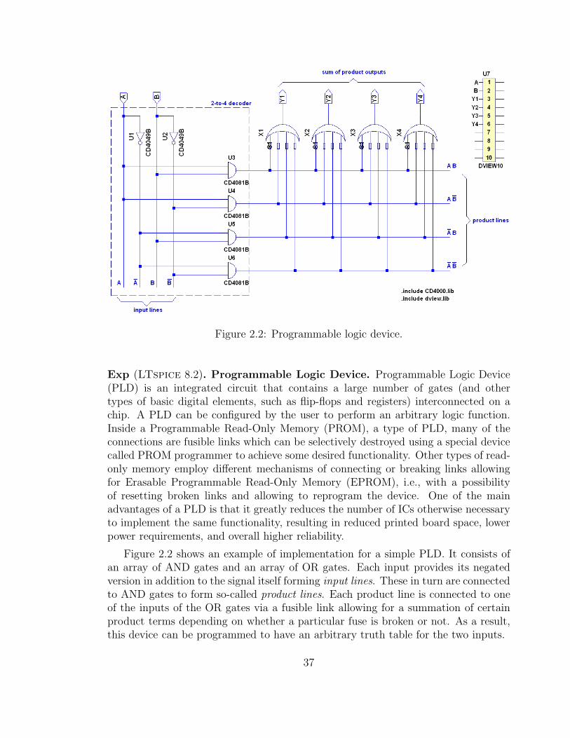
Figure 2.2: Programmable logic device.
Exp (LTspice 8.2). Programmable Logic Device. Programmable Logic Device(PLD) is an integrated circuit that contains a large number of gates (and othertypes of basic digital elements, such as flip-flops and registers) interconnected on achip. A PLD can be configured by the user to perform an arbitrary logic function.Inside a Programmable Read-Only Memory (PROM), a type of PLD, many of theconnections are fusible links which can be selectively destroyed using a special devicecalled PROM programmer to achieve some desired functionality. Other types of read-only memory employ different mechanisms of connecting or breaking links allowingfor Erasable Programmable Read-Only Memory (EPROM), i.e., with a possibilityof resetting broken links and allowing to reprogram the device. One of the mainadvantages of a PLD is that it greatly reduces the number of ICs otherwise necessaryto implement the same functionality, resulting in reduced printed board space, lowerpower requirements, and overall higher reliability.
Figure 2.2 shows an example of implementation for a simple PLD. It consists ofan array of AND gates and an array of OR gates. Each input provides its negatedversion in addition to the signal itself forming input lines. These in turn are connectedto AND gates to form so-called product lines. Each product line is connected to oneof the inputs of the OR gates via a fusible link allowing for a summation of certainproduct terms depending on whether a particular fuse is broken or not. As a result,this device can be programmed to have an arbitrary truth table for the two inputs.
37

The example on Figure 2.2 has 2 input lines and 4 output lines. Implement thiscircuit in LTspice. To do so, copy the contents of SPICE\experiments\8.2to your local directory. It contains: symbols for CMOS gates CD4049B (NOT),CD4072B (4-input OR), CD4081B (AND), and CD4000.lib SPICE library file withtheir definitions (also found in SPICE\external_components\Digital_CD4000
directory); a circuit block files (fuse4or.asy and fuse4or.asc) that implement4-input OR gate with “fusible” links; a single-pole double-throw switch sym-bol spdt.asy and its model switches.sub (also available in switches direc-tory in SPICE\external_components); and a “component” to simultaneouslyview digital traces (dview10.asy and dview.lib), which can also be found inSPICE\external_components\dview directory. Build the circuit using 2 NOTgates, 4 AND gates, and 4 fusible 4-input OR gates (use fuse4or, not CD4072B).
Right-click on one of the fusible 4-input OR gates to see how this subcircuit isimplemented. The 4 switches represent “fuses”. By default, these “fuses” connectthe OR gate to its inputs. A “fuse” can be “blown” by passing a parameter to thesubcircuit. From your PLD circuit, right-click on one of the four OR gates, then enter,for example, S1=0 S3=0 in PARAMS field. A corresponding text will appear next tothe gate’s symbol if you place a checkmark next to PARAMS. These parameters will“blow” S1 and S3 “fuses” producing 0 logic on the corresponding inputs of the ORgate, regardless of the input. The position of S1 input is shown in the symbol to helpyou identify how the input pins are connected to the corresponding “fuses”: S1, S2,S3, and S4.
Implement the following Boolean functions by “blowing” the appropriate “fuses”:A XOR B on Y1; NOT A on Y2 (regardless of B); A OR B on Y3; A NOR B on Y4.Write down each of these functions as they correspond to their implementationin the circuit (i.e., in terms of sums of products). Supply square 0-5V pulses oninputs A and B (1:2 frequency ratio) to verify the truth table for each of the 4functions by viewing the corresponding outputs.
2.2 Chapter 9 Experiments
Exp (LTspice 9.1). Master-slave RS and JK flip-flops. Figure 2.3 shows animplementation of a negative-edge triggered RS flip-flop. It employs a master-slaveconfiguration, in which two identical clocked RS latches are used. An individualclocked latch performs as a regular RS latch when the clock input CLK is logic 1. IfCLK level is logic 0, S and R inputs have no effect on the latch, and it retains its oldvalue.
Note that the two CLK inputs are connected via an inverter. This ensures thatthe two sections will be enabled during opposite half-cycles of the clock signal. Thisis key to realizing an edge-triggered flip-flop.
38

Q
Q
S
R
CLK
master slave
S1
R1
S2
R2
Q1
Q1
Figure 2.3: Master-slave configuration for RS flip-flop.
Consider what happens when CLK input starts out at logic 0 level. The S andR inputs are disconnected from the input (master) latch. Therefore, any changes inthe input signals cannot affect the state of the final outputs. When the CLK signalgoes 1, the S and R inputs are able to control the master latch. However, at the sametime, the inverted CLK signal applied to the slave latch prevents the master latchfrom having any effect on it. This way any changes in the R and S input signals arepropagated to Q1 and Q1 by the master latch while CLK is at 1, but are not reflectedin the Q and Q outputs.
When CLK falls back to 0, the S and R inputs are again isolated from the masterlatch. At the same time, the inverted CLK signal now allows the current state of themaster latch (Q1 and Q1) to reach the output latch. Thus, the Q and Q outputscan only change state when the CLK signal falls from logic 1 to 0. This is known asnegative (falling) edge triggered RS flip-flop.
Construct this circuit in LTspice using 74HCT00 NAND and 74HCT04 invertergates (found in SPICE\external_components\Digital_74HCTxxx). You candraw wires diagonally in LTspice by holding down Ctrl key. 74HCT is a populardigital family that uses CMOS technology but is also compatible with TTL signallevels. Be sure to include the appropriate library file 74HCT.LIB. Supply voltagesignals (0-5V levels) to S, R, and CLK, as shown in Figure 2.4 (use PWL optionto specify piece-wise linear functions for S and R inputs — accessible after right-clicking on the voltage source, then pressing Advanced button).
To avoid the circuit’s going into a “race” (rapid oscillations of the outputs withsteady inputs), supply the following initial conditions:.ic V(Q)=0 V(_Q)=5 V(Q1)=0 V(_Q1)=5
39

Figure 2.4: Signals (0-5V range) for LTspice Exp. 9.1.
where Q, _Q, Q1, and _Q1 are the node labels for Q, Q, Q1, and Q1, respectively.This sets both RS latches to 0 initial state.
Fill out the following table:S R CLK Q0 0 ! 01 0 !0 0 !0 1 !0 0 !
You can also send this circuit into a “race” by supplying S = R = 1. Such undefinedbehavior is an intrinsic limitation of RS flip-flops. You can turn this circuit into a JKflip-flop that does not have such a problem. First, you need to replace the two NAND
gates at the input with two 3-input NANDs. Use 74HCT10 3-input NAND gates. Todeal with the problematic S = R = 1 condition, one should discretely disable thiscondition from propagating into the master latch while keeping all other combinationsunaltered. The basic idea is that one has to disable S input when and only when Qis 1 (S input’s job is done, no need to reassert it continuously), and also to disable Rinput when Q = 0 (R input’s job is done, no need to reassert it continuously). Onecan do so by connecting the remaining 3rd input of each 74HCT10 NAND to theappropriate output.
Turn your original circuit into a JK flip-flop. Verify that the circuit works byrunning it with inputs as shown in Figure 2.4.
40

Fill out the following table:S R CLK Q0 0 ! 01 0 !0 0 !0 1 !0 0 !1 1 !1 1 !0 0 !
Exp (LTspice 9.2). Domino effect in a ripple counter.
Build two different 8-bit counters using the appropriate HCT family components:an asynchronous one using 8 D flip-flops 74HCT74 and a synchronous one using2 4-bit binary counters 74HCT161. As usual, copy the symbols and the corre-sponding library file from SPICE\external_components\Digital_74HCTxxx toyour local directory. Supply a clock CLK signal (0-5V) of 100kHz frequency toboth counters. Name synchronous counter bits S0 through S7, and asynchronouscounter bits A0 through A7.
To visualize a difference between the two counters, you can perform a digital-to-analog “conversion” on their outputs: convert the binary representation of thecounter’s state into a signal of varying amplitude that can be visualized. One simpleway to accomplish it in LTspice is to add a special voltage source to your circuit, aso-called behavioral voltage source. The output of such a source in LTspice can beprogrammed with an arbitrary function. To insert this special component, select bv
symbol from Select Component Symbol window after pressing F2 . Insert two suchsources (one for each counter). Right-click on each of the components and enter thefollowing strings in their respective Value fields:V=(V(S0)+2*V(S1)+4*V(S2)+8*V(S3)+16*V(S4)+32*V(S5)+64*V(S6)+128*V(S7))/255
andV=(V(A0)+2*V(A1)+4*V(A2)+8*V(A3)+16*V(A4)+32*V(A5)+64*V(A6)+128*V(A7))/255
If the counter bit outputs are strictly 0 or 5V, these functions will convert the binaryvalues represented by these bits (digital) to a voltage in a 0-5V range (analog).
Run the simulation on these two counters for 4ms. Plot analog signals obtainedfrom the digital-to-analog conversion of the outputs for each case. You shouldsee a sawtooth pattern in both cases. How does that pattern differ between thesynchronous and asynchronous versions? Zoom in on the largest “glitch”, whichoccurs half-way between 0 and 5V. Write down binary values that the counter goesthrough during that “glitch” and their corresponding voltage values.
41
2.3 Chapter 10 Experiments
Figure 2.5: Circuit for LTspice Exp. 10.1: Missing Pulse Detector.
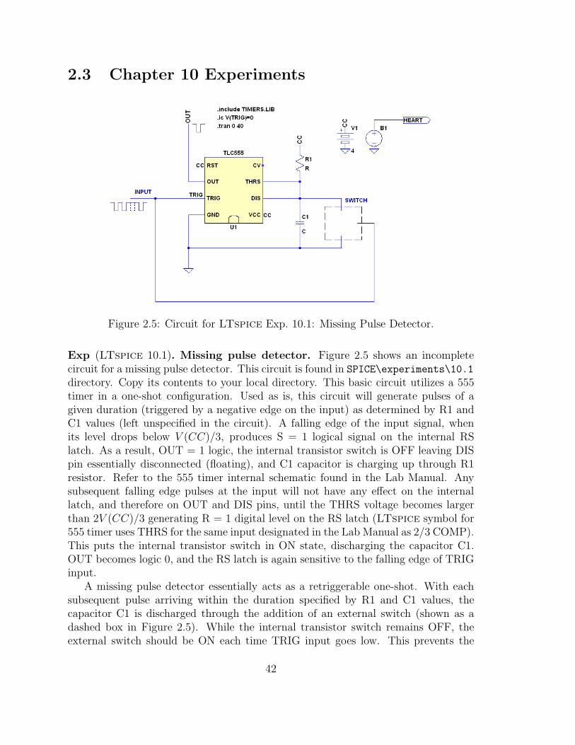
Exp (LTspice 10.1). Missing pulse detector. Figure 2.5 shows an incompletecircuit for a missing pulse detector. This circuit is found in SPICE\experiments\10.1
directory. Copy its contents to your local directory. This basic circuit utilizes a 555timer in a one-shot configuration. Used as is, this circuit will generate pulses of agiven duration (triggered by a negative edge on the input) as determined by R1 andC1 values (left unspecified in the circuit). A falling edge of the input signal, whenits level drops below V (CC)/3, produces S = 1 logical signal on the internal RSlatch. As a result, OUT = 1 logic, the internal transistor switch is OFF leaving DISpin essentially disconnected (floating), and C1 capacitor is charging up through R1resistor. Refer to the 555 timer internal schematic found in the Lab Manual. Anysubsequent falling edge pulses at the input will not have any effect on the internallatch, and therefore on OUT and DIS pins, until the THRS voltage becomes largerthan 2V (CC)/3 generating R = 1 digital level on the RS latch (LTspice symbol for555 timer uses THRS for the same input designated in the Lab Manual as 2/3 COMP).This puts the internal transistor switch in ON state, discharging the capacitor C1.OUT becomes logic 0, and the RS latch is again sensitive to the falling edge of TRIGinput.
A missing pulse detector essentially acts as a retriggerable one-shot. With eachsubsequent pulse arriving within the duration specified by R1 and C1 values, thecapacitor C1 is discharged through the addition of an external switch (shown as adashed box in Figure 2.5). While the internal transistor switch remains OFF, theexternal switch should be ON each time TRIG input goes low. This prevents the
42
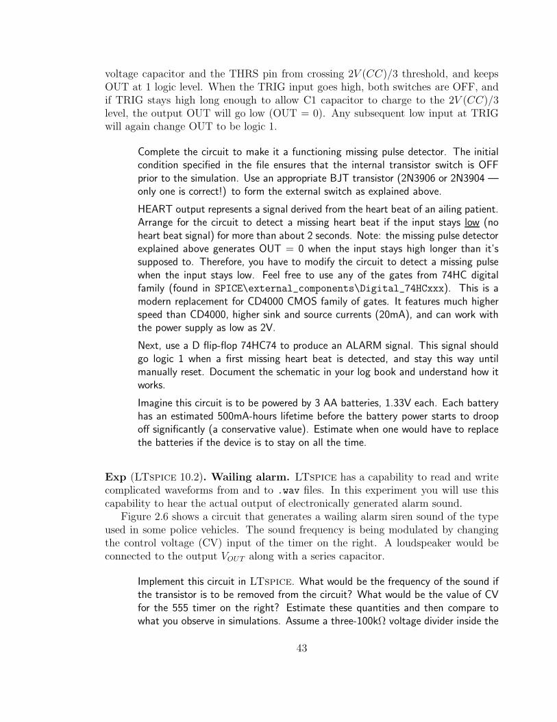
voltage capacitor and the THRS pin from crossing 2V (CC)/3 threshold, and keepsOUT at 1 logic level. When the TRIG input goes high, both switches are OFF, andif TRIG stays high long enough to allow C1 capacitor to charge to the 2V (CC)/3level, the output OUT will go low (OUT = 0). Any subsequent low input at TRIGwill again change OUT to be logic 1.
Complete the circuit to make it a functioning missing pulse detector. The initialcondition specified in the file ensures that the internal transistor switch is OFFprior to the simulation. Use an appropriate BJT transistor (2N3906 or 2N3904 —only one is correct!) to form the external switch as explained above.
HEART output represents a signal derived from the heart beat of an ailing patient.Arrange for the circuit to detect a missing heart beat if the input stays low (noheart beat signal) for more than about 2 seconds. Note: the missing pulse detectorexplained above generates OUT = 0 when the input stays high longer than it’ssupposed to. Therefore, you have to modify the circuit to detect a missing pulsewhen the input stays low. Feel free to use any of the gates from 74HC digitalfamily (found in SPICE\external_components\Digital_74HCxxx). This is amodern replacement for CD4000 CMOS family of gates. It features much higherspeed than CD4000, higher sink and source currents (20mA), and can work withthe power supply as low as 2V.
Next, use a D flip-flop 74HC74 to produce an ALARM signal. This signal shouldgo logic 1 when a first missing heart beat is detected, and stay this way untilmanually reset. Document the schematic in your log book and understand how itworks.
Imagine this circuit is to be powered by 3 AA batteries, 1.33V each. Each batteryhas an estimated 500mA-hours lifetime before the battery power starts to droopoff significantly (a conservative value). Estimate when one would have to replacethe batteries if the device is to stay on all the time.
Exp (LTspice 10.2). Wailing alarm. LTspice has a capability to read and writecomplicated waveforms from and to .wav files. In this experiment you will use thiscapability to hear the actual output of electronically generated alarm sound.
Figure 2.6 shows a circuit that generates a wailing alarm siren sound of the typeused in some police vehicles. The sound frequency is being modulated by changingthe control voltage (CV) input of the timer on the right. A loudspeaker would beconnected to the output VOUT along with a series capacitor.
Implement this circuit in LTspice. What would be the frequency of the sound ifthe transistor is to be removed from the circuit? What would be the value of CVfor the 555 timer on the right? Estimate these quantities and then compare towhat you observe in simulations. Assume a three-100kΩ voltage divider inside the
43

RST
TRIGGND
OUTTHRS
DISVCC
CV
555timer
1 5
3
2
6
7
8 4 8 4
RST
OUT3
CV
51
GNDTRIG
THRS
VCCDIS
555timer
6
7
2
0.01µF
C2+
R1B
R1A
4.7kΩ
47kΩ
0.01µF
C1
100µF
R2A
10kΩ
R2B
100kΩ
2.7kΩ
4.7kΩ
Q1
2N3906
VOUT
+5V
Figure 2.6: Circuit generating wailing alarm siren sound.
555 instead of 5kΩ.With the transistor in place, note the maximum and minimumvoltages at CV. When is the pitch higher: when CV is high or low?
To generate a .wav file, add the following SPICE directive to your circuit:.wave "somename.wav" 16 22.05K V(OUT)
This line instructs LTspice to write the waveform of V(OUT) to a file somename.wav
with 16 sampling bits at the sampling frequency of 22.05kHz (more on what thatmeans later in the course). The .wav analog to digital converter in LTspice has afull scale range of ±1V. For best results the signal to be written to a .wav file has tomatch that range, otherwise, the converted signal will end up being truncated.
The output of the circuit is in 0-5V range. Build a simple voltage divider at theoutput of the circuit to transform the signal to ±1V range (you will also needa voltage source to shift the signal). Move OUT node label to the new outputlocation with ±1V signal (in real life you could drive a speaker connected througha series capacitor directly from the output in Figure 2.6). Simulate the circuit forabout 15s and listen to the sound that it produces by playing the .wav file (itwill appear in the same directory as your .asc file with the schematic). Try fewdifferent values of C1 in the range from 1 to 100µF. Observe the change in thesound by recording and playing different .wav files.
2.4 Chapter 11 Experiment
Exp (LTspice 11.1). Signal encryption using a sequence of pseudo-random
numbers. Random numbers that lack any order have many uses in computational
44
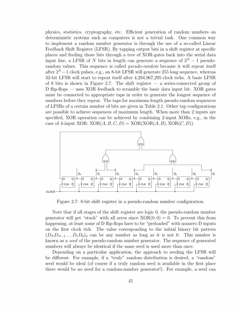
physics, statistics, cryptography, etc. Efficient generation of random numbers ondeterministic systems such as computers is not a trivial task. One common wayto implement a random number generator is through the use of a so-called LinearFeedback Shift Register (LFSR). By tapping output bits in a shift register at specificplaces and feeding those bits through a tree of XOR-gates back into the serial datainput line, a LFSR of N bits in length can generate a sequence of 2N − 1 pseudo-random values. This sequence is called pseudo-random because it will repeat itselfafter 2N −1 clock pulses, e.g., an 8-bit LFSR will generate 255 long sequence, whereas32-bit LFSR will start to repeat itself after 4,294,967,295 clock ticks. A basic LFSRof 8 bits is shown in Figure 2.7. The shift register — a series-connected group ofD flip-flops — uses XOR feedback to scramble the basic data input bit. XOR gatesmust be connected to appropriate taps in order to generate the longest sequence ofnumbers before they repeat. The taps for maximum-length pseudo-random sequencesof LFSRs of a certain number of bits are given in Table 2.1. Other tap configurationsare possible to achieve sequences of maximum length. When more than 2 inputs arespecified, XOR operation can be achieved by combining 2-input XORs, e.g., in thecase of 4-input XOR: XOR(A, B, C, D) = XOR(XOR(A, B), XOR(C, D)).
D
CLK
Q
Q
D Q
QCLK
D Q
QCLK
D Q
QCLK
D Q
QCLK
D Q
QCLK
D Q
QCLK
D Q
QCLK
CLOCK
Q0 Q4 Q5 Q6 Q7Q1 Q2 Q3
Figure 2.7: 8-bit shift register in a pseudo-random number configuration.
Note that if all stages of the shift register are logic 0, the pseudo-random numbergenerator will get “stuck” with all zeros since XOR(0, 0) = 0. To prevent this fromhappening, at least some of D flip-flops have to be “preloaded” with nonzero D inputson the first clock tick. The value corresponding to the initial binary bit pattern(DNDN−1 . . .D1D0)2 can be any number as long as it is not 0. This number isknown as a seed of the pseudo-random number generator. The sequence of generatednumbers will always be identical if the same seed is used more than once.
Depending on a particular application, the approach to seeding the LFSR willbe different. For example, if a “truly” random distribution is desired, a “random”seed would be ideal (of course if a truly random seed is available in the first placethere would be no need for a random-number generator!). For example, a seed can
45
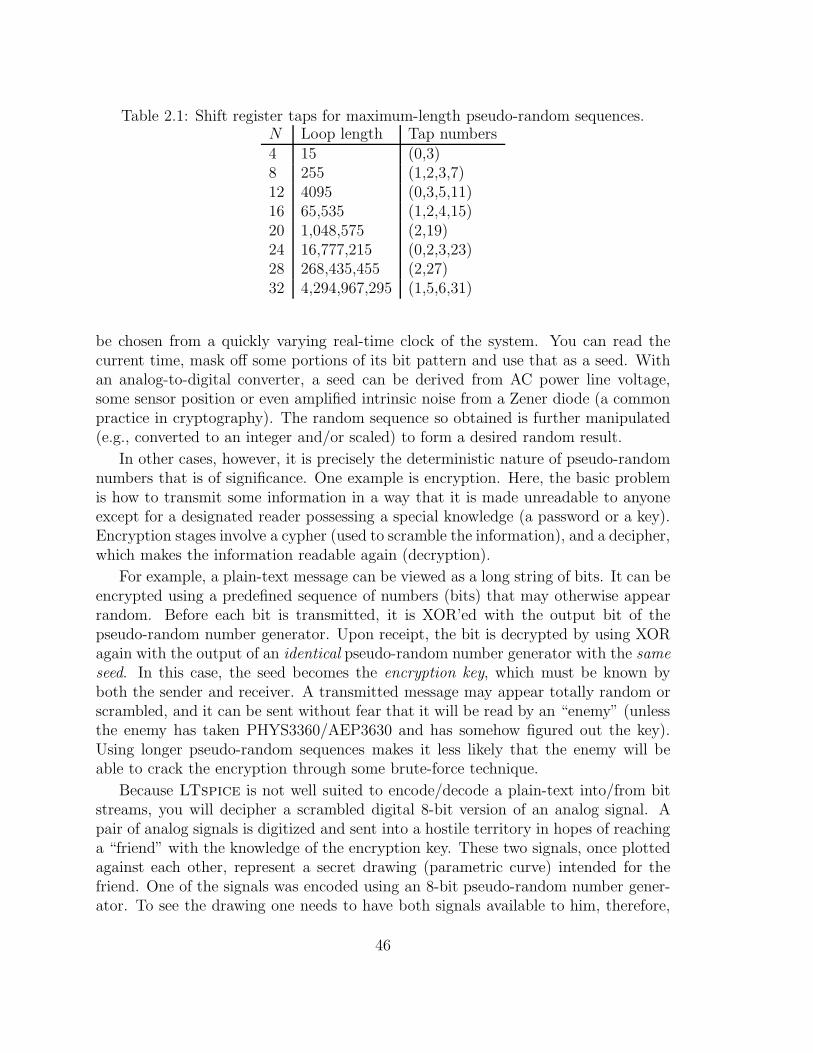
Table 2.1: Shift register taps for maximum-length pseudo-random sequences.N Loop length Tap numbers4 15 (0,3)8 255 (1,2,3,7)12 4095 (0,3,5,11)16 65,535 (1,2,4,15)20 1,048,575 (2,19)24 16,777,215 (0,2,3,23)28 268,435,455 (2,27)32 4,294,967,295 (1,5,6,31)
be chosen from a quickly varying real-time clock of the system. You can read thecurrent time, mask off some portions of its bit pattern and use that as a seed. Withan analog-to-digital converter, a seed can be derived from AC power line voltage,some sensor position or even amplified intrinsic noise from a Zener diode (a commonpractice in cryptography). The random sequence so obtained is further manipulated(e.g., converted to an integer and/or scaled) to form a desired random result.
In other cases, however, it is precisely the deterministic nature of pseudo-randomnumbers that is of significance. One example is encryption. Here, the basic problemis how to transmit some information in a way that it is made unreadable to anyoneexcept for a designated reader possessing a special knowledge (a password or a key).Encryption stages involve a cypher (used to scramble the information), and a decipher,which makes the information readable again (decryption).
For example, a plain-text message can be viewed as a long string of bits. It can beencrypted using a predefined sequence of numbers (bits) that may otherwise appearrandom. Before each bit is transmitted, it is XOR’ed with the output bit of thepseudo-random number generator. Upon receipt, the bit is decrypted by using XORagain with the output of an identical pseudo-random number generator with the same
seed. In this case, the seed becomes the encryption key, which must be known byboth the sender and receiver. A transmitted message may appear totally random orscrambled, and it can be sent without fear that it will be read by an “enemy” (unlessthe enemy has taken PHYS3360/AEP3630 and has somehow figured out the key).Using longer pseudo-random sequences makes it less likely that the enemy will beable to crack the encryption through some brute-force technique.
Because LTspice is not well suited to encode/decode a plain-text into/from bitstreams, you will decipher a scrambled digital 8-bit version of an analog signal. Apair of analog signals is digitized and sent into a hostile territory in hopes of reachinga “friend” with the knowledge of the encryption key. These two signals, once plottedagainst each other, represent a secret drawing (parametric curve) intended for thefriend. One of the signals was encoded using an 8-bit pseudo-random number gener-ator. To see the drawing one needs to have both signals available to him, therefore,
46

encrypting only one signal is sufficient to scramble the information being transmitted.There are several subtleties to this simple encryption method. First, in addition to
having to use identical pseudo-random number generator, the clocks used to encryptand decipher the signal must be identical as well. The sequence of pseudo-randomnumbers must overlap exactly with the encrypted signal, which inevitably brings upthe issue of synchronization. As such, the technique described here can be reliablyused only on relatively short messages (as limited by the clock accuracy). Second,even if the encrypted signal and the proper sequence of pseudo-random numbersoverlap, special attention is still required for the edges as determined by the clocksignal. For example, the propagation delay in XOR gates used for decryption maycause “glitches” at the edges of the signal once converted to analog form (similar tothe domino effect in the case of asynchronous counter). One simple way to fix thisproblem is to pass all the bits of the signal as a final stage through D flip-flops clockedwith a timing signal edge sufficiently delayed with respect to the master clock activeedge to ensure that all transients have died out by that time. For example, if the shiftregister is triggered by the positive edge of the master clock, you can use the negativeedge of the clock to clean up the signal. Doing so effectively delays the signal. If thereis another signal which must be synchronous with the first, it too should be passedthrough D flip-flops triggered by the same clock signal.
Decipher a secret message which was encrypted using a sequence of pseudo-random 8-bit numbers. Copy the contents of SPICE\experiments\11.1 to yourlocal directory. The files include some relevant devices from the 74HC digitalfamily (symbols 74hc04.asy, 74hc86.asy, 74hc374.asy, and the library file74hc.lib). There are two behavioral components to be used in the circuit: an8-port buffer to boost the level of digital signals to 5V (buf8.asy symbol andbuf8.asc schematic files), and a component which performs digital (8-bit) toanalog (±1V default range) conversion (dac8.asy file and dac8.asc schematicfiles). These components are called behavioral because they only act like theirreal-life counterparts, while they are implemented using behavioral voltage sourcesin LTspice, as opposed to electronic components, such as transistors, capaci-tors, etc. The directory also contains the schematic file encryption.asc and twotraces containing the “transmitted” information: xtrace_encrypted.wav andytrace.wav. Open encryption.asc file with LTspice. See Figure 2.8.
There are several areas in this schematic (partially filled): Digital Input, ClockSignal, Pseudo-Random Number Generator (RNG), Cypher/Decipher, Edge Clean-Up, and Digital to Analog. In the Digital Input area, you will find two traces in8-bit digital form loaded from the .wav files: encrypted x-trace and y-trace signal.When y-trace is plotted against x-trace, it will display the secret drawing. Youcan see that each bit is imported from an appropriate channel in .wav file. Note:LTspice can read and write .wav files which may not be playable for soundbecause of the number of channels being used, the number of sampling bits or
47

Figure 2.8: Unfinished schematic for LTspice Exp. 11.1: Signal Encryption.
the sampling rate. These files, however, are useful to store complicated signals forLTspice simulations.
The two signals in 8-bit digital form are available at nodes EX0 (LSB) throughEX7 (MSB) for the encrypted x-trace, and SY0 through SY7 for the y-trace. Tovisualize these traces, place two digital to analog converters (dac8) in Digital toAnalog area, one for each trace. Connect appropriate inputs of DACs to the 8bits of each signal. (Hint: use node labels for connections!) Plot the resultantanalog signals against each other and observe a scrambled pattern. The job is nowto decipher the x-trace represented by (EX7EX6EX5EX4EX3EX2EX1EX0)2
binary value.
First, construct a LFSR random number generator. In Pseudo-Random NumberGenerator (RNG) area, connect the pins of 74HC374 — a positive edge-triggeredoctal D flip-flop — to form a shift register. Use small value resistors (e.g. 1Ω) toconnect the appropriate pins on the right of the 74HC374. The reason for usingsmall resistors is just a matter of convenience: LTspice allows only a single labelper a set of nodes connected with wires, whereas we would prefer to address theinput and output pins of the flip-flop by different labels: DX0 (LSB) through DX7
(MSB) and QX0 through QX7, respectively. Verify that the shift register works bysupplying logic 1 (5V) to DX0 (use the .ic line in the schematic) and observing thevalue propagating along the output bits. Note: the full simulation loading entiretrace signals may take several minutes. To verify that various subcomponentswork properly, it is sufficient to simulate the circuit only for a small fraction of the
48
entire time span. This can be accomplished through pressing Halt icon afterthe simulation has been started. Next, setup XOR gates as shown in Figure 2.7or given in Table 2.1. Observe that the LFSR is working by supplying 1 logic toone of DX inputs. You may hook up QX outputs of RNG to DAC and observe theanalog representation of the output.
Second, build a decipher by XOR’ing the bits of the RNG output QX and theencrypted signal EX.
Third, perform edge clean-up by passing both decrypted x-trace and y-trace bitsthrough a pair of 74HC374’s triggered off the negative edge of CLK clock signal.Then connect both 8-bit digital outputs to DACs.
You are now ready to decrypt the secret message. An instruction in place of a keysimply states: “last two digits of your Alma Mater founding date”.
Use the hint provided to decrypt the message. Convert the last two digits in thefounding date of the University to binary form and use it in place of the seed forLFSR (.ic line in the schematic). Display y-trace vs. decrypted x-trace. Youmay choose Mark Data Points from Plot Settings drop-down Menu to better seeindividual points on the plot.
The operations of encryption/decryption are reversible in this case. E.g. you canuse this circuit to encrypt the signal with your own choice of the seed such as theyear of your graduation.
2.5 Chapter 12 Experiments
Exp (LTspice 12.1). Dual-Slope Analog to Digital Converter. IntegratingA/D converters (ADCs) employ a very different principle compared to convertersthat require a “frozen” input, such as a flash or successive approximation ADC. Astheir name implies, the output of integrating ADCs represents the integral or averageof an input voltage over a fixed period of time. This results in a good immunityto high frequency noise (relative to the measurement period), albeit at the expenseof a reduced speed of the A/D conversion. Integrating ADCs are ideal for use inmeasuring devices, such as digital voltmeters and panel meters. In fact, the overallusage of integrating converters exceeds the combined total of all other conversionmethods.
A particular representation of this class of ADCs is a dual-slope converter. Fig-ure 2.9 illustrates its working principle. Dual-slope A/D converter involves a 2-stageprocess. First, S1 switch is closed to ensure capacitor C is discharged. The counter isreset. S2 switch is then connected to Vin input voltage about to be measured. Vin isintegrated for a fixed time tm = m/f0, where m is the number of clock ticks allowed
49

−
+−
+−
+
S1
S2
Vref
Vin
CTRL
CLK
coutnerbinary
digital output
C
R
comparatorintegrator
inverting buffer
vi
Figure 2.9: Dual slope A/D converter.
for a measurement, and f0 is the reference clock frequency. The voltage at the outputof the integrator after time tm is then given by
vi =1
RC
∫
Vindt =tmRC
〈Vin〉 .
For the second stage, S2 switch is thrown immediately after time tm to a well con-trolled reference voltage −Vref of the opposite sign to Vin (alternatively, one of thesetwo signals can be connected to the integrator via an inverter). At the same time thecounter starts to count. After some time tr, vi integrates back to zero, the comparatorgoes HIGH stopping the counter. The counter reading represents the digital value of〈Vin〉. The slopes of the integrator in these two stages are proportional to the voltagesupplied, namely Vin and −Vref . Hence the name of the method. So, the two timeperiods, the fixed measurement time tm when S2 switch is connected to Vin, and theintegrator’s capacitor discharge time tr from the reference voltage −Vref are relatedby
tmRC
〈Vin〉 =tr
RCVref .
If r is the number of clock ticks counted by the counter during the discharge time ofthe capacitor, tr = r/f0, Vin is simply given by
〈Vin〉 =r
mVref .
This is an elegant result. The digital representation of the measured voltage endsup being independent from the integrator’s time constant RC and the clock frequencyf0! This means the design is extremely forgiving with respect to tolerances of thecomponent values. As a drawback of the dual-slope converter, one may point outthe long time required for a single A/D conversion, which ends up being at least(r + m)/f0. Nevertheless, a good fraction of this time is used to average the inputsignal Vin, improving the signal-to-noise ratio of the measurement.
50
Figure 2.10: Circuit for LTspice Exp. 12.1: Dual-Slope A/D Converter.
Copy the file from SPICE\experiments\12.1 to your local directory. This filecontains an implementation of a dual-slope ADC. It uses several parameters:zero_ticks refers to how many clock cycles the capacitor stays shorted out atthe beginning of the measurement; meas_ticks specifies how many cycles the in-tegrator is to be connected to the (inverse) input voltage. The clock frequency f0
and the reference voltage Vref specify additional parameters for the ADC. Spendsome time familiarizing yourself with how this circuit works. Plot various switchvoltages: sw_zero, sw_meas, and sw_ref versus time. The circuit contains sev-eral sample input signals: +3V DC voltage (sig_clean), 3V with 1V 60Hz ACsignal superimposed on top (sig_acnoise), and 3V signal with some white noiseof 2V peak-to-peak amplitude (sig_whitenoise). Connect sig_acnoise to theinput of the ADC, and observe the voltage at the input and output of the inte-grator. The circuit also contains a gated counter implemented from 8 D flip-flops.View the voltage at the counter’s node gated_clk during the various stages ofA/D conversion.
Next, connect the 3V input signal sig_clean. The digitized output of the counteris converted back to analog domain to ease its visualization. View the voltage onsum_cleaned node. Note that the output had to be cleaned to get rid of the edge“glitches” (compare this to the unrefined voltage signal at sum node). Changevalues of R, C, and f0 by 10% to double-check that the output of the dual-slopeconverter does not depend on these values.
Connect the noisy signal sig_whitenoise to the converter’s input. Find theRMS value of the input signal and compare it to the error of the measured voltage(relative to 3V).
Finally, connect sig_acnoise back to the ADC input. Note the error in the
51

measured voltage relative to 3V. A certain choice of f0 frequency can be used tototally reject 60Hz AC line noise. Find the expression for such frequency values.(Hint: it should contain both m and 60Hz). Verify that the noise is fully suppressedwhen you assign f0 a value from your formula.
52
Exp (LTspice 12.2). Noise analysis in LTspice. Noise comes in many ways andforms. By noise we understand any unwanted electrical disturbance. Such distur-bances can be classified either as intrinsic noise or as interference. Interferences areintroduction of external sources of noise or other signals to the electric circuit throughvarious coupling mechanisms, such as mechanical, electromagnetic, etc. These typesof noise can be largely suppressed through a proper design, shielding techniques,and so on. Intrinsic noise, on the other hand, is a property of individual components,which cannot be completely eliminated. Understanding the origin of different types ofnoise, their identification, characterization, and subsequent mitigation often requiresconsiderable knowledge and experience. Some additional information is available inthe following books [5, 6, 7]. Here we will briefly touch on intrinsic noise types and use.noise analysis available in LTspice to estimate a noise figure of a simple commonemitter amplifier.
The following three types of intrinsic noise are being considered: i) Johnson (ther-mal) noise, ii) shot noise, and iii) flicker noise.
Johnson noise is an intrinsic noise, which arises due to thermal fluctuations of thenumber of current carriers in two halves of a resistor. Any resistor, no matter howexpensive, displays this type of noise. The rms voltage that appears on the resistorR is given by
vn,rms =√
4kBTR∆f,
where Boltzmann’s constant kB = 1.38 × 10⁻²³J/K, T is the resistor’s temperaturein Kelvin, and ∆f is the measurement bandwidth (or the response of the circuit) inHerz. For example, Johnson noise for R = 20kΩ in audio frequency range (∆f ≈20kHz) at T = 300K is vn,rms = 2.5µV. Johnson noise power spectrum (power perunit bandwidth) is independent of frequency, and such types of noise are oftentimesreferred to as “white” (various frequencies are equally represented). Because of the∝
√∆f dependance of the voltage on the bandwidth for “white” noise, it is common
to specify this and other types of noise as voltage spectral noise density in units ofV/
√Hz. To find the rms voltage equivalent, one has to multiply the spectral noise
density by the square root of the bandwidth (provided the spectral noise density is aconstant).
The shot noise appears due to discrete charge of the electron, and the corre-sponding statistical fluctuations in current (also known as “rain on a tin roof” noise).Poisson statistics tells us that fluctuations in a stochastic (random) quantity, suchas a number of radioactive decays per second, number of cars in traffic passing anobserver per unit time, etc., are proportional to the square root of the mean numberof events. Similarly, the rms current fluctuation due to shot noise is proportional tothe square root of the signal current is, which is given by
in,rms =√
2eis∆f.
Here e = 1.6×10⁻¹⁹C is the electron’s charge and ∆f is the measurement bandwidth.Similar to Johnson noise, shot noise has a “white” spectrum.
53

Flicker noise or “1/f” noise has power spectrum that follows 1/f trend, domi-nating the noise spectrum at low frequencies. Unlike the two other types of intrinsicnoise, flicker noise does not have a single physical mechanism behind it, but is insteada cumulative term that encompasses a number of noise generating mechanisms, suchas carrier density fluctuations in semiconductor devices. Flicker noise dominates atlow frequencies over Johnson and shot noise, and it depends on such properties of thecomponent’s material as purity, dopant levels, etc.
To characterize noise magnitude relative to the signal’s strength, it is common touse signal-to-noise ratio — a ratio of power contained in the signal over that of thenoise:
SNRdB = 10 log10(Ps/Pn) = 20 log10(Vs/Vn).
Another parameter being used (especially in RF circuitry) is noise figure, which spec-ifies how much additional noise is being introduced by the circuit (NFdB > 0 always):
NFdB = 20 log10
(Vs/Vn)in
(Vs/Vn)out
= SNRin
dB− SNRout
dB.
SPICE (and LTspice) provides a capability of modeling circuit performance in thepresence of intrinsic noise. The analysis is limited to frequency domain. Components,such as diodes and transistors, have model parameters that specify their flicker noisebehavior (usually it is necessary to double-check that these parameters have beenproperly assigned in each specific SPICE model before performing noise analysis).The command for noise analysis has the following syntax:.noise V(<out>[,<ref>]) <src> <oct,dec,lin> <Npoints> <StartFreq> <EndFreq>
V(<out>[,<ref>]) is the node at which the total output noise is calculated. It can beexpressed as V(n1,n2) to represent the voltage between two nodes. <src> is the nameof an independent source (a noiseless input signal) to which input noise is referred.The parameters <oct,dec,lin>, <Nsteps>, <StartFreq>, and <EndFreq> define thefrequency range of interest and resolution in the manner used in the .ac directive.For example:.noise V(OUT) Vin dec 10 1K 1MEG
instructs SPICE to calculate noise at OUT node using frequency sweep with 10 pointsper decade starting from 1kHz to 1MHz. The corresponding input noise will bereferred to Vin source. The analysis produces output data trace V(onoise) accessiblefor plotting by clicking on OUT node. V(onoise) is a noise spectral voltage densityreferenced to the OUT node specified as the output in the above syntax. It will haveunits of V/
√Hz. To find total rms voltage noise, one needs to integrate spectral
voltage density V(onoise) over a range of frequencies of interest (i.e., the bandwidth).It can be done by pressing Ctrl key and left-clicking on V(onoise) legend in the plotwindow. Additionally, the analysis produces trace V(inoise), which represents theinput-referred noise voltage density. It is simply V(onoise) divided by the AC gainof OUT relative to the input source Vin.
54

By default, the temperature of 27C is assumed for Johnson noise. You can changethis parameter using .temp <temp_in_celcius> SPICE directive in the circuit.
+15V
RB1
RB2
Rin
RC
RE
Rout
Cout
Cin
CE
1kΩ
15kΩ
2.2kΩ
3.6kΩ
680Ω
0.1µF100kΩ
1µF
10µF
2N3904
out
Vin+−
1kΩ sourceimpedance
Figure 2.11: Common emitter amplifier for LTspice Exp. 12.2: Noise Analysis.
Implement a common-emitter amplifier in LTspice as shown in Figure 2.11. Per-form noise analysis on OUT node for a frequency range 100Hz to 5MHz. Observethe noise spectral voltage V(onoise).
Next, obtain a plot of the noise figure vs. frequency for this circuit. To do so,enter 20*log10(V(onoise)/V(Rin)) expression in the plotting utility window.This compares noise levels at Rin input resistor to that of the output OUT, whichis the definition of noise figure. Observe 1/f behavior in the noise figure at lowfrequencies. What do you think is the cause of this behavior?
Next, determine vn,rms that you would measure from the output of this circuitwith an ideal scope that has a perfect response from DC to 5MHz frequency (inthe absence of additional noise sources and interference). Determine the signal-to-noise ratio expressed in dB for a signal that has an rms voltage of vs,rms = 0.5V.
55

Bibliography
[1] http://tech.groups.yahoo.com/group/LTspice
[2] http://www.winehq.org
[3] For example, a free software project gEDA contains a utility program PCB forproducing printed circuit boards http://geda.seul.org. A number of other freePCB utilities exist that support netlists to help ensure correct connections,see for example http://www.freepcb.com, http://www.expresspcb.com, andhttp://www.pad2pad.com.
[4] Most manufacturers’ websites provide SPICE models for their analog devices.Also refer to [1] for a large collection of user-created components (both digitaland analog)
[5] G. Vasilescu, Electronic Noise and Interfering Signals: Principles and Applica-
tions, Springer, 2005.
[6] P. Horowitz, W. Hill, The Art of Electronics, 2nd Edition, Cambridge UniversityPress, 1989. Sections 7.11-25 and 15.12-15.
[7] R.E. Simpson, Introductory Electornics, 2nd Edition, Allen and Bacon, 1987.Chapter 8.
56

Index
.ac, 20
.ic, 24
.include, 25
.lib, 25
.meas, 18–19
.noise, 53
.op, 16
.param, 18
.step, 18, 24
.subckt, 22, 30
.tran, 10–11
.wave, 44
ADCdual slope, 49
analysisnoise, see .noise
Q-point, see .op
small gain, see .ac
time-transient, see .tran
astable multivibrator, 24
behavioral voltage source, 41Bode plot, 20, 33
circuit block, 30viewing signals in, 31
CMOS, 36common-emitter amplifier, 55component
placement, 7
selection, 7custom component, 29
model, 29symbol, 27
assigning ports in, 28, 30
DAC8-bit, 47using behavioral voltage source, 41
digital family74HC, 4374HCT, 39CD4000, 43specifying components, 25
diodespecifying, 13, 34
dview, 35
ECAD, 3Electr. Comp.-Aided Design, see ECADexternal models, 21
flip-flopJK, 40master-slave configuration, 38RS, 38
high-pass filter, 7
LFSR, 45library files, 25, 35
digital components, 25, 35
57

Linear Feedback Shift Reg., see LFSRLTspice, 3, 7
Control Panel, 11, 31help on, 7plotting utility, 12waveform viewer, 12
missing pulse detector, 42mixed mode of simulation, 3
netlist, 5–6, 14, 16noise, 53
figure of, 54flicker, 54Johnson, 53shot noise, 53thermal, see Johnson noise
op-ampcustom model, 30model file for LM741, 21specifying, 21
PLD, 37EPROM, 37PROM, 37
Programmable Logic Device, see PLDpseudo-random number generator, 45
rectifierfull-wave, 33
ring oscillator, 25ripple counter
asynchronous, 41domino effect, 41synchronous, 41
schematic capture, 6, 7signal encryption, 44signal-to-noise ratio, 54SPICE, 5
directives, 6, 10–15, 21SPICE3, 5XSPICE, 5
SwitcherCad, see LTspice
timer 555specifying, 42
transformercenter-tapped, 33specifying, 33
transistorspecifying, 15, 32
units, 9decimal prefixes, 9
voltage follower, 21closed loop gain, 33loop gain, 33stability margin, 32
voltage sourcespecifying, 10
waveform arithmetic, 13
58