Embed Size (px)
Citation preview
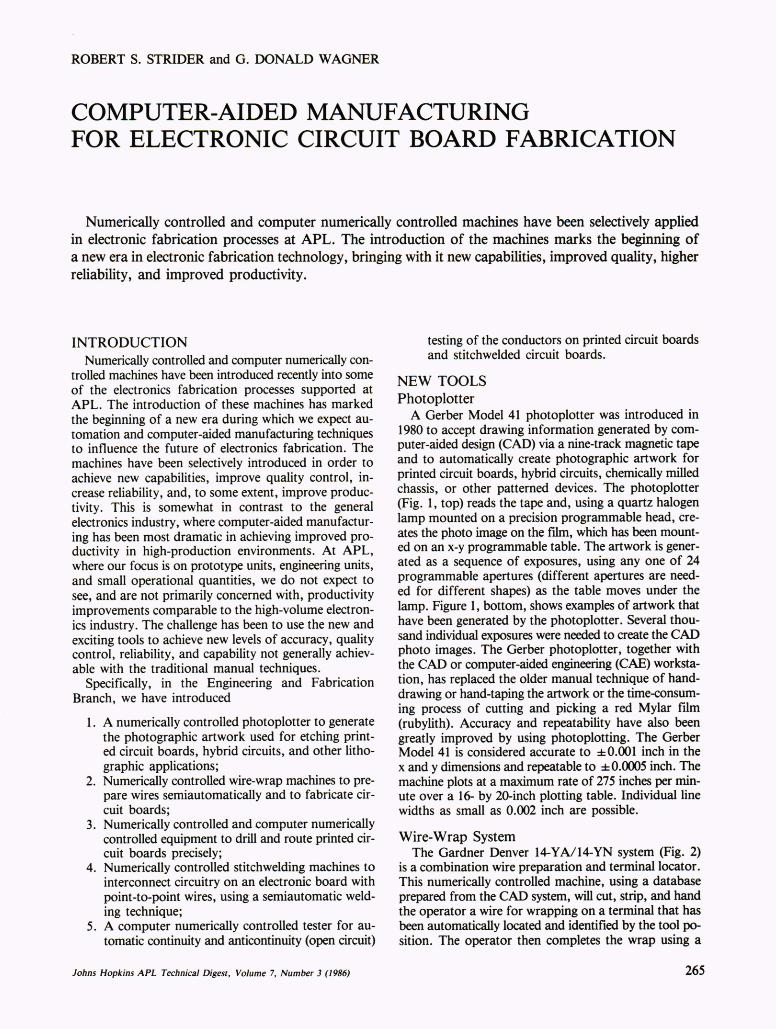
ROBERT S. STRIDER and G. DONALD WAGNER
COMPUTER-AIDED MANUFACTURING FOR ELECTRONIC CIRCUIT BOARD FABRICATION
Numerically controlled and computer numerically controlled machines have been selectively applied in electronic fabrication processes at APL. The introduction of the machines marks the beginning of a new era in electronic fabrication technology, bringing with it new capabilities, improved quality, higher reliability, and improved productivity.
INTRODUCTION Numerically controlled and computer numerically con
trolled machines have been introduced recently into some of the electronics fabrication processes supported at APL. The introduction of these machines has marked the beginning of a new era during which we expect automation and computer-aided manufacturing techniques to influence the future of electronics fabrication. The machines have been selectively introduced in order to achieve new capabilities, improve quality control, increase reliability, and, to some extent, improve productivity. This is somewhat in contrast to the general electronics industry, where computer-aided manufacturing has been most dramatic in achieving improved productivity in high-production environments. At APL, where our focus is on prototype units, engineering units, and small operational quantities, we do not expect to see, and are not primarily concerned with, productivity improvements comparable to the high-volume electronics industry. The challenge has been to use the new and exciting tools to achieve new levels of accuracy, quality control, reliability, and capability not generally achievable with the traditional manual techniques.
Specifically, in the Engineering and Fabrication Branch, we have introduced
1. A numerically controlled photoplotter to generate the photographic artwork used for etching printed circuit boards, hybrid circuits, and other lithographic applications;
2. Numerically controlled wire-wrap machines to prepare wires semiautomatically and to fabricate circuit boards;
3. Numerically controlled and computer numerically controlled equipment to drill and route printed circuit boards precisely;
4. Numerically controlled stitchwelding machines to interconnect circuitry on an electronic board with point-to-point wires, using a semiautomatic welding technique;
5. A computer numerically controlled tester for automatic continuity and anticontinuity (open circuit)
Johns Hopkins APL Technical Digest, Volume 7, Number J (1986)
testing of the conductors on printed circuit boards and stitch welded circuit boards.
NEW TOOLS Photoplotter
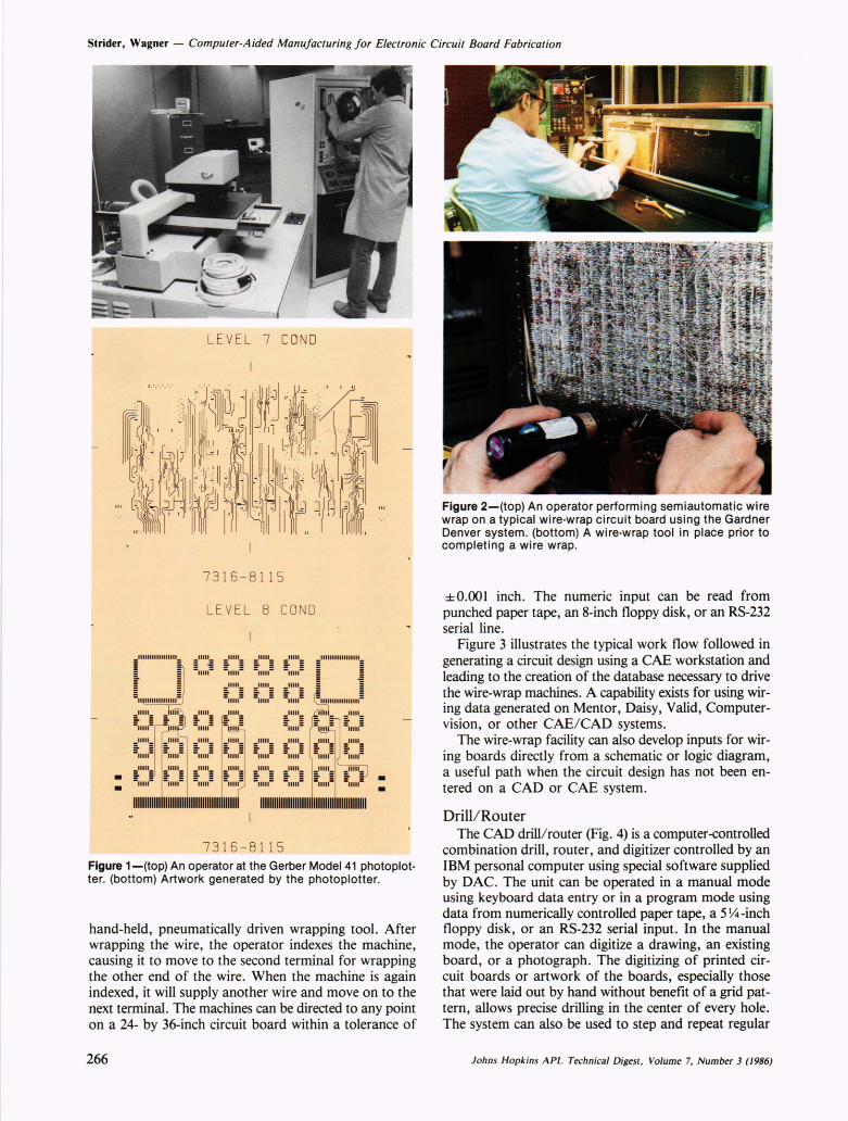
A Gerber Model 41 photoplotter was introduced in 1980 to accept drawing information generated by computer-aided design (CAD) via a nine-track magnetic tape and to automatically create photographic artwork for printed circuit boards, hybrid circuits, chemically milled chassis, or other patterned devices. The photoplotter (Fig. 1, top) reads the tape and, using a quartz halogen lamp mounted on a precision programmable head, creates the photo image on the fIlm, which has been mounted on an x-y programmable table. The artwork is generated as a sequence of exposures, using anyone of 24 programmable apertures (different apertures are needed for different shapes) as the table moves under the lamp. Figure 1, bottom, shows examples of artwork that have been generated by the photoplotter. Several thousand individual exposures were needed to create the CAD photo images. The Gerber photoplotter, together with the CAD or computer-aided engineering (CAE) workstation, has replaced the older manual technique of handdrawing or hand-taping the artwork or the time-consuming process of cutting and picking a red Mylar film (rubylith). Accuracy and repeatability have also been greatly improved by using photoplotting. The Gerber Model 41 is considered accurate to ±0.001 inch in the x and y dimensions and repeatable to ± 0.0005 inch. The machine plots at a maximum rate of 275 inches per minute over a 16- by 20-inch plotting table. Individual line widths as small as 0.002 inch are possible.
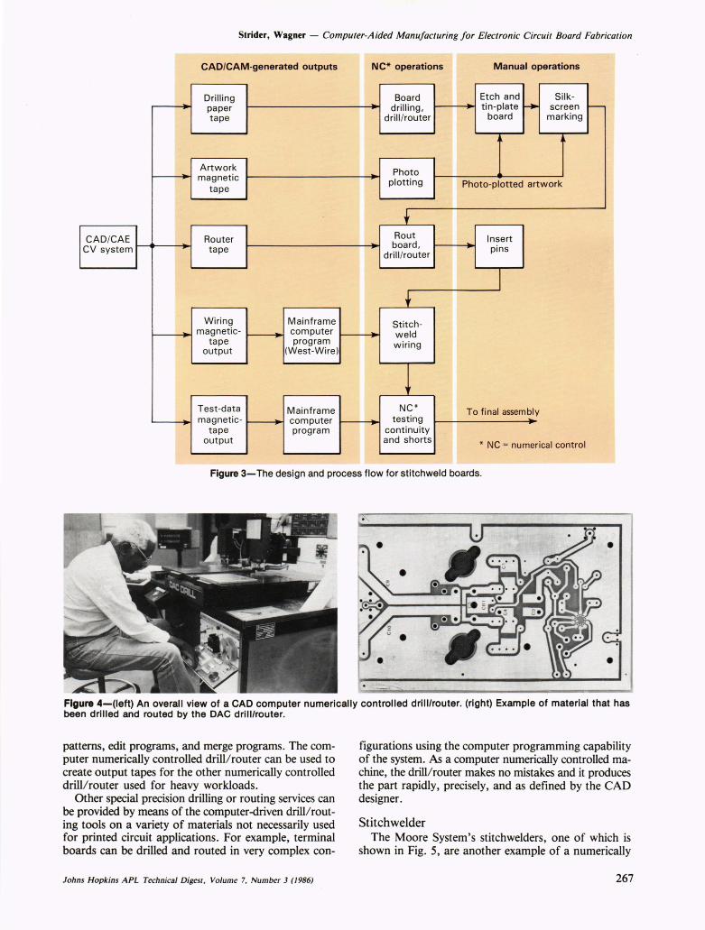
Wire-Wrap System The Gardner Denver 14-YAlI4-YN system (Fig. 2)
is a combination wire preparation and terminal locator . This numerically controlled machine, using a database prepared from the CAD system, will cut, strip, and hand the operator a wire for wrapping on a terminal that has been automatically located and identified by the tool position. The operator then completes the wrap using a
265
Strider, Wagner - Computer-Aided Manufacturing for Electronic Circuit Board Fabrication
LEVEL 7 [OND
7316-8115
LEVEL 8 [OND
11111 11111 11111 11111 11111111111111111
-11111 - -11111 - -11111 - -11111 - I I 11111 11111 11111
-11111 - -11111 - -11111 - ~IIIIIIIIIIIII~ ~IIII~ 11111 ~IIII~ ~IIE ~IIII~ :.
11111 - III - 11111 III 11111
~IIII~ 11111 11111 11111 11111 11111 ~IIII~ 11111
11111 -11111 - -11111 - -11111 - -11111 - -11111 - 11111 =11111=
~IIII; ~IIII~ ~IIII~ 11111 ~IIII~ allll: ~IIII~ 11111
• • • 11111 11111 11111 =11111= 11111 =11111= 11111 =11111=
• 111111111111111111111111111111111111111111 11111111111111111111111111111111111111111111
7316-8115 Figure 1-(top) An operator at the Gerber Model 41 photoplot· ter. (bottom) Artwork generated by the photoplotter.
hand-held, pneumatically driven wrapping tool. After wrapping the wire, the operator indexes the machine, causing it to move to the second terminal for wrapping the other end of the wire. When the machine is again indexed, it will supply another wire and move on to the next terminaL The machines can be directed to any point on a 24- by 36-inch circuit board within a tolerance of
266
f ,
Figure 2-(top) An operator performing semiautomatic wire wrap on a typical wire·wrap circuit board using the Gardner Denver system. (bottom) A wire-wrap tool in place prior to completing a wire wrap.
±O.OOI inch. The numeric input can be read from punched paper tape, an 8-inch floppy disk, or an RS-232 serial line.
Figure 3 illustrates the typical work flow followed in generating a circuit design using a CAE workstation and leading to the creation of the database necessary to drive the wire-wrap machines. A capability exists for using wiring data generated on Mentor, Daisy, Valid, Computervision, or other CAE/CAD systems.
The wire-wrap facility can also develop inputs for wiring boards directly from a schematic or logic diagram, a useful path when the circuit design has not been entered on a CAD or CAE system .
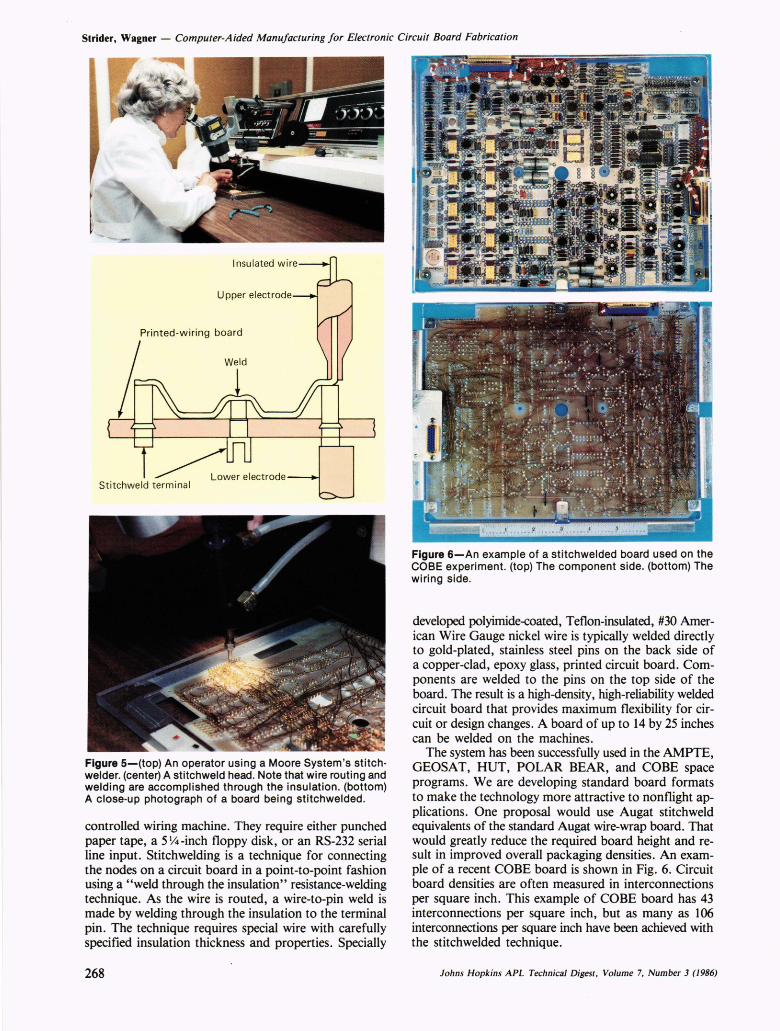
Drill/Router The CAD drill/router (Fig. 4) is a computer-controlled
combination drill, router, and digitizer controlled by an IBM personal computer using special software supplied by DAC. The unit can be operated in a manual mode using keyboard data entry or in a program mode using data from numerically controlled paper tape, a 5 Y4 -inch floppy disk, or an RS-232 serial input. In the manual mode, the operator can digitize a drawing, an existing board, or a photograph. The digitizing of printed circuit boards or artwork of the boards, especially those that were laid out by hand without benefit of a grid pattern, allows precise drilling in the center of every hole. The system can also be used to step and repeat regular
Johns Hopkins APL Technical Digest . Volume 7. Number 3 (/986)
Strider, Wagner - Computer-Aided Manufacturing for Electronic Circuit Board Fabrication
CAD/CAM-generated outputs NC* operations Manual operations
Drilling Board Etch and Silk-paper drilling,
.. tin-plate f-+ screen -tape drill/router board marking
Artwork Photo magnetic plotting Photo-plotted artwork tape
I f
CAD/CAE Router Rout Insert board, ..
CV system , tape , pins
drill/router
t Wiring Mainframe Stitch-
magnetic- computer , weld tape program wiring
output (West-Wire)
~ Test-data Mainframe NC* To final assembly magnetic- computer I testing --"" ,
! I tape program continuity output and shorts
* NC = numerical control
Figure 3-The design and process flow for stitchweld boards.
•
•
Figure 4-(left) An overall view of a CAD computer numerically controlled drill/router. (right) Example of material that has been drilled and routed by the DAC drill/router.
patterns, edit programs, and merge programs. The computer numerically controlled drill/router can be used to create output tapes for the other numerically controlled drill/router used for heavy workloads.
Other special precision drilling or routing services can be provided by means of the computer-driven drill/routing tools on a variety of materials not necessarily used for printed circuit applications. For example, terminal boards can be drilled and routed in very complex con-
Johns Hopkins APL Technical Digest, Volume 7, Number 3 (/986)
figurations using the computer programming capability of the system. As a computer numerically controlled machine, the drill/router makes no mistakes and it produces the part rapidly, precisely, and as defined by the CAD designer.
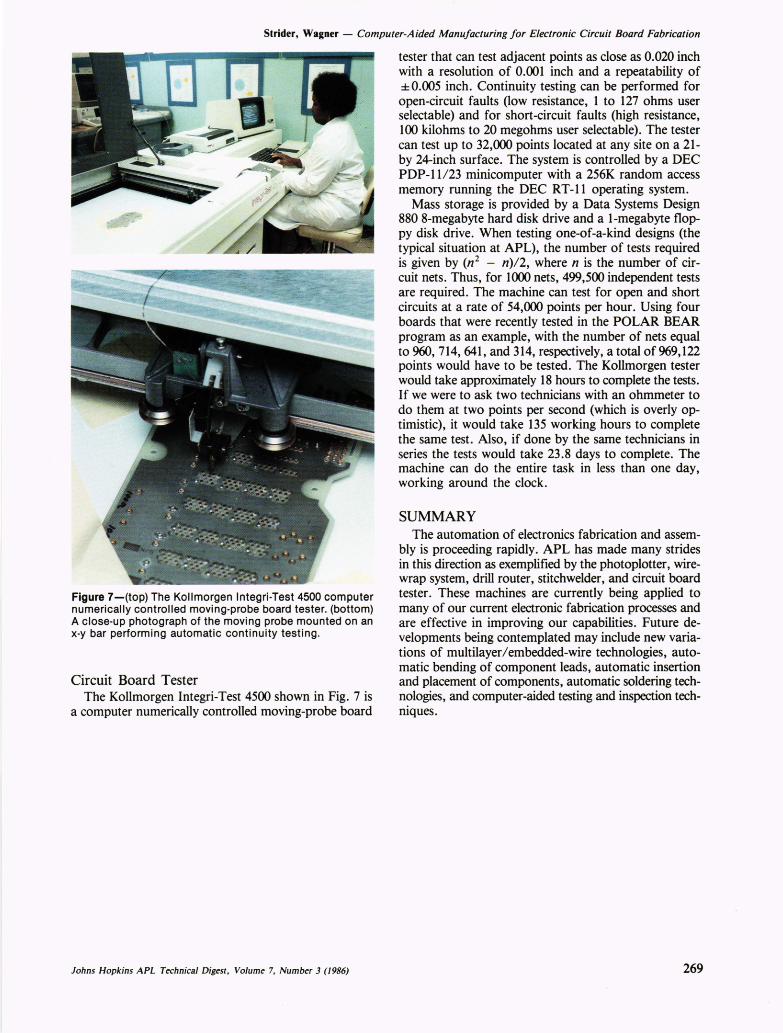
Stitch welder The Moore System's stitchwelders, one of which is
shown in Fig. 5, are another example of a numerically
267
Strider, Wagner - Computer-Aided Manufacturing for Electronic Circuit Board Fabrication
Lower electrode Stitchweld terminal
Figure 5-(top) An operator using a Moore System's stitchwelder. (center) A stitchweld head. Note that wire routing and welding are accomplished through the insulation. (bottom) A close-up photograph of a board being stitchwelded.
controlled wiring machine. They require either punched paper tape, a 5 Y4-inch floppy disk, or an RS-232 serial line input. Stitchwelding is a technique for connecting the nodes on a circuit board in a point-to-point fashion using a "weld through the insulation" resistance-welding technique. As the wire is routed, a wire-to-pin weld is made by welding through the insulation to the terminal pin. The technique requires special wire with carefully specified insulation thickness and properties. Specially
268
Figure 6-An example of a stitchwelded board used on the COBE experiment. (top) The component side. (bottom) The wiring side.
developed polyimide-coated, Teflon-insulated, #30 American Wire Gauge nickel wire is typically welded directly to gold-plated, stainless steel pins on the back side of a copper-clad, epoxy glass, printed circuit board. Components are welded to the pins on the top side of the board. The result is a high-density, high-reliability welded circuit board that provides maximum flexibility for circuit or design changes. A board of up to 14 by 25 inches can be welded on the machines.
The system has been successfully used in the AMPTE, GEOSAT, HUT, POLAR BEAR, and CO BE space programs. We are developing standard board formats to make the technology more attractive to non flight applications. One proposal would use Augat stitch weld equivalents of the standard Augat wire-wrap board. That would greatly reduce the required board height and result in improved overall packaging densities. An example of a recent COBE board is shown in Fig. 6. Circuit board densities are often measured in interconnections per square inch. This example of COBE board has 43 interconnections per square inch, but as many as 106 interconnections per square inch have been achieved with the stitchwelded technique.
Johns Hopkins APL Technical Digest , Volume 7, Number 3 (1986)
Strider, Wagner - Computer-Aided Manufacturing for Electronic Circuit Board Fabrication
Figure 7-(top) The Kollmorgen Integri-Test 4500 computer numerically controlled moving-probe board tester. (bottom) A close-up photograph of the moving probe mounted on an x-y bar performing automatic continuity testing.
Circuit Board Tester The Kollmorgen Integri-Test 4500 shown in Fig. 7 is
a computer numerically controlled moving-probe board
Johns Hopkins APL Technical Digest, Volume 7, Number 3 (1986)
tester that can test adjacent points as close as 0.020 inch with a resolution of 0.001 inch and a repeatability of ±0.005 inch. Continuity testing can be performed for open-circuit faults (low resistance, 1 to 127 ohms user selectable) and for short-circuit faults (high resistance, 100 kilohms to 20 megohms user selectable). The tester can test up to 32,000 points located at any site on a 21-by 24-inch surface. The system is controlled by a DEC PDP-11123 minicomputer with a 256K random access memory running the DEC RT-ll operating system.
Mass storage is provided by a Data Systems Design 880 8-megabyte hard disk drive and a I-megabyte floppy disk drive. When testing one-of-a-kind designs (the typical situation at APL), the number of tests required is given by (n 2
- n)/2, where n is the number of circuit nets. Thus, for 1000 nets, 499,500 independent tests are required. The machine can test for open and short circuits at a rate of 54,000 points per hour. Using four boards that were recently tested in the POLAR BEAR program as an example, with the number of nets equal to 960,714,641, and 314, respectively, a total of 969,122 points would have to be tested. The Kollmorgen tester would take approximately 18 hours to complete the tests. If we were to ask two technicians with an ohmmeter to do them at two points per second (which is overly optimistic), it would take 135 working hours to complete the same test. Also, if done by the same technicians in series the tests would take 23.8 days to complete. The machine can do the entire task in less than one day, working around the clock.
SUMMARY The automation of electronics fabrication and assem
bly is proceeding rapidly. APL has made many strides in this direction as exemplified by the photoplotter, wirewrap system, drill router, stitch welder , and circuit board tester. These machines are currently being applied to many of our current electronic fabrication processes and are effective in improving our capabilities. Future developments being contemplated may include new variations of multilayer/embedded-wire technologies, automatic bending of component leads, automatic insertion and placement of components, automatic soldering technologies, and computer-aided testing and inspection techniques.
269
Strider, Wagner - Computer-Aided Manufacturing for Electronic Circuit Board Fabrication
THE AUTHORS
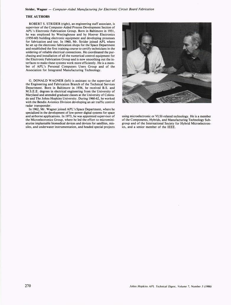
ROBERT S. STRIDER (right), an engineering staff associate, is supervisor of the Computer-Aided Process Development Section of APL's Electronic Fabrication Group. Born in Baltimore in 1931, he was employed by Westinghouse and by Hoover Electronics (1950-60) building electronic equipment and developing processes for fabrication and test. In 1960, Mr. Strider joined APL where he set up the electronic fabrication shops for the Space Department and established the first training course to certify technicians in the soldering of reliable electrical connections. He coordinated the purchasing and installation of all the numerical control equipment for the Electronic Fabrication Group and is now smoothing out the interfaces to make these systems work more efficiently. He is a member of APL's Personal Computers Users Group and of the Association for Integrated Manufacturing Technology.
G. DONALD WAGNER (left) is assistant to the supervisor of the Engineering and Fabrication Branch of the Technical Services Department. Born in Baltimore in 1936, he received B.S. and M.S.E.E. degrees in electrical engineering from the University of Maryland and attended graduate classes at the University of Colorado and The Johns Hopkins University. During 1960-62, he worked with the Bendix Avionics Division developing an air traffic control radar transponder.
In 1962, Mr. Wagner joined APL's Space Department, where he specialized in the development of low-power digital systems for space and airborne applications . In 1973, he was appointed supervisor of the Microelectronics Group, where he led the effort to microminiaturize implantable biomedical devices and devices for satellites, missiles, and underwater instrumentation, and headed special projects
270
using microelectronic or VLSI-related technology. He is a member of the Components, Hybrids, and Manufacturing Technology Subgroup and of the International Society for Hybrid Microelectronics, and a senior member of the IEEE.
Johns Hopkins APL Technical Digest , Volume 7, Number 3 (/986)