Embed Size (px)
Citation preview

Electronic Circuits 10CS32
Dept. of CSE, SJBIT 1
ELECTRONIC CIRCUITS
Subject Code: 10CS32 I.A. Marks : 25
Hours/Week : 04 Exam Hours: 03
Total Hours : 52 Exam Marks: 100
PART - A
UNIT – 1 7 Hours
Transistors, UJTs, and Thyristors:
Operating Point, Common-EmitterConfiguration, Thermal Runaway, Transistor Switch,
Unijunction Transistors, SCR.
UNIT – 2 6 Hours
Field Effect Transistors:
Bipolar Junction Transistors versus Field Effect Transistors, Junction Field Effect Transistors,
Metal Oxide Field Effect Transistors, Differences between JFETs and MOSFETs, Handling
MOSFETs, Biasing MOSFETs, FET Applications, CMOS Devices, Insulated Gate Bipolar
Transistors (IGBTs)
UNIT – 3 6 Hours
Optoelectronic Devices:
Introduction, Photosensors, Photoconductors, Photodiodes, Phototransistors, Light-Emitting
Diodes, Liquid Crystal Displays, Cathode Ray Tube Displays, Emerging Display Technologies,
Optocouplers
UNIT – 4 7 Hours
Small Signal Analysis of Amplifiers:
Amplifier Bandwidth: General Frequency Considerations, Hybrid h-Parameter Model for an
Amplifier, Transistor Hybrid Model, Analysis of a Transistor Amplifier using complete h-
Parameter Model, Analysis of a Transistor Amplifier Configurations using Simplified h-
Parameter Model (CE configuration only), Small-Signal Analysis of FET Amplifiers, Cascading
Amplifiers, Darlington Amplifier, Low-Frequency Response of Amplifiers (BJT amplifiers
only).
PART – B
UNIT - 5 6 Hours
Large Signal Amplifiers, Feedback Amplifier:
Classification and characteristics of Large Signal Amplifiers, Feedback Amplifiers:
Classification of Amplifiers, Amplifier with Negative Feedback, Advantages of Negative
Feedback, Feedback Topologies, Voltage-Series (Series-Shunt) Feedback, Voltage-Shunt
(Shunt-Shunt) Feedback, Current-Series (Series- Series) Feedback, Current-Shunt (Shunt-
Series)Feedback.

Electronic Circuits 10CS32
Dept. of CSE, SJBIT 2
UNIT - 6 7 Hours
Sinusoidal Oscillators, Wave-Shaping Circuits:
Classification of Oscillators, Conditions for Oscillations: Barkhausen Criterion, Types of
Oscillators, Crystal Oscillator, Voltage-Controlled Oscillators, Frequency Stability. Wave-
Shaping Circuits: Basic RC Low-Pass Circuit, RC Low-Pass Circuit as Integrator, Basic RC
High-Pass Circuit, RC High-Pass Circuit as Differentiator, Multivibrators, Integrated Circuit (IC)
Multivibrators.
UNIT - 7 7 Hours
Linear Power Supplies, Switched mode Power Supplies:
Linear Power Supplies: Constituents of a Linear Power Supply, Designing Mains Transformer;
Linear IC Voltage Regulators, Regulated Power Supply Parameters. Switched Mode Power
Supplies: Switched Mode Power Supplies, Switching Regulators, Connecting Power Converters
in Series, Connecting Power Converters in Parallel.
UNIT - 8 6 Hours
Operational Amplifiers: Ideal Opamp versus Practical Opamp, Performance Parameters, Some
Applications: Peak Detector Circuit, Absolute Value Circuit, Comparator, Active Filters, Phase
Shifters, Instrumentation Amplifier, Non-Linear Amplifier, Relaxation Oscillator, Current-To-
Voltage Converter, Voltage-To-Current Converter, Sine Wave Oscillators.
Text Book:
1. Anil K Maini, Varsha Agarwal: Electronic Devices and Circuits, Wiley, 2009.
(4.1, 4.2, 4.7, 4.8, 5.1 to 5.3, 5.5, 5.6, 5.8, 5.9, 5.13, 5.14, 6.1, 6.3, 7.1 to 7.5, 7.10 to 7.14, Listed
topics only from 8, 10.1, 11, 12.1, 12.2, 12.3, 12.5, 13.1 to 13.6, 13.9, 13.10, 14.1, 14.2, 14.6,
14.7, 15.1, 15.5 to 15.7. 16.3, 16.4, 17.12 to 17.22)
Reference Books:
1. Jacob Millman, Christos Halkias, Chetan D Parikh: Millman‟s Integrated Electronics – Analog
and Digital Circuits and Systems, 2nd Edition, Tata McGraw Hill, 2010. 2. R. D. Sudhaker Samuel: Electronic Circuits, Sanguine-Pearson

Electronic Circuits 10CS32
Dept. of CSE, SJBIT 3
Table of Contents
Unit – 1: Transistor, UJT‟s, and Thyristors ............................................................................ 5
1.1 Operating Point ............................................................................................................ 5
1.2 The Common Emitter (CE) Configuration ................................................................. 10
1.3 The Transistor as a Switch ......................................................................................... 23
1.4 Silicon-Controlled Rectifiers, or SCRs ....................................................................... 31
1.5 The Gate Turn-Off Thyristors (GTO) ......................................................................... 32
1.6 Recommended Questions ........................................................................................... 41
Unit – 2: Bipolar Junction Transistors.................................................................................. 43
2.1 Bipolar junction transistor (BJT) ................................................................................ 43
2.2 The Field Effect Transistor ........................................................................................ 48
2.3 The Junction Field Effect Transistor .......................................................................... 50
2.4 Comparison of connections between a JFET and a BJT.............................................. 50
2.5 JFET Amplifier .......................................................................................................... 55
2.6 CMOS ....................................................................................................................... 56
2.7 Recommended Questions ........................................................................................... 58
Unit – 3: Photodiodes .......................................................................................................... 59
3.1 Photodiodes ............................................................................................................... 59
3.2 PN Photodiode ........................................................................................................... 59
3.3 PIN Photodiode ......................................................................................................... 60
3.4 Schottky Photodiode .................................................................................................. 60
3.5 Phototransistors ......................................................................................................... 63
3.6 Light-Emitting Diodes (LED) .................................................................................... 64
3.7 Cathode Ray Tube Displays ....................................................................................... 70
3.8 Emerging Display Technologies ................................................................................ 71
3.9 Optocouplers ............................................................................................................. 72
3.10 Recommended Questions ......................................................................................... 74
UNIT – 4: Small Signal Analysis of Amplifiers ................................................................... 75
4.1 Basic FET Amplifiers ................................................................................................ 75
4.2 THE MOSFET AMPLIFIER ..................................................................................... 75
4.3 Small-Signal Equivalent Circuit ................................................................................. 81
4.4 Problem-Solving Technique: MOSFET AC Analysis ................................................. 83
4.5 Basic Transistor Amplifier Configurations ................................................................. 85
4.6 The Source-Follower Amplifer .................................................................................. 92

Electronic Circuits 10CS32
Dept. of CSE, SJBIT 4
4.7 Input and Output impedance ...................................................................................... 95
4.8 The Common-Gate Configuration .............................................................................. 96
4.9 The Three Basic Amplifier Configurations: Summary and Comparison ..................... 99
4.10 Recommended Questions ....................................................................................... 102
Unit – 5: Large Signal Amplifiers ...................................................................................... 103
5.1 Classification of Large Signal Amplifiers................................................................. 103
5.2 Large signal Amplifier Characteristics ..................................................................... 105
5.3 Feedback Amplifiers ................................................................................................ 107
5.4 Stability of Gain Factor ............................................................................................ 109
5.5 Feedback Topologies ............................................................................................... 111
5.6 Recommended Questions ......................................................................................... 112
UNIT – 6: Sinusoidal Oscillators ....................................................................................... 113
6.1 Principles of oscillators ............................................................................................ 113
6.2 Phase shift Oscillator ............................................................................................... 119
6.3 Band Pass Oscillators ............................................................................................... 125
6.4 Wien Bridge Oscillator ............................................................................................ 128
6.5 Colpitts and Hartley Oscillators ............................................................................... 131
6.6 Piezoelectric Crystal Oscillators ............................................................................... 138
6.7 Recommended Questions ......................................................................................... 153
UNIT – 7: Linear Power Supplies, Switched mode Power Supplies ................................... 154
7.1 Regulated power supply ........................................................................................... 154
7.2 POWER SUPPLY FILTER ..................................................................................... 154
7.3 Fixed Positive Linear Voltage Regulators ................................................................ 157
7.4 The Regulated Dual Voltage DC Power Supply ....................................................... 161
7.5 Recommended Questions ......................................................................................... 163
UNIT – 8: Operational Amplifier....................................................................................... 164
8.1 Operational Amplifier (Op-Amp) ............................................................................. 164
8.2 Ideal Op-Amp .......................................................................................................... 166
8.3 Applications of Opamp ............................................................................................ 168
8.4 Instrumentation Amplifier ........................................................................................ 178
8.5 Relaxation Oscillator ............................................................................................... 180
8.6 Current-to-Voltage Converter .................................................................................. 181
8.7 Voltage-to-Current Converter .................................................................................. 181
8.8 Exercise Problems ................................................................................................... 182

Electronic Circuits 10CS32
Dept. of CSE, SJBIT 5
Unit – 1: Transistor, UJT’s, and Thyristors
In the Diode tutorials we saw that simple diodes are made up from two pieces of semiconductor
material, either silicon or germanium to form a simple PN-junction and we also learnt about their
properties and characteristics. If we now join together two individual signal diodes back-to-back,
this will give us two PN-junctions connected together in series that share a common P or N
terminal. The fusion of these two diodes produces a three layer, two junctions, and three terminal
devices forming the basis of a Bipolar Junction Transistor, or BJT for short.
1.1 Operating Point
Operating Regions
The pink shaded area at the bottom of the curves represents the "Cut-off" region while the blue
area to the left represents the "Saturation" region of the transistor. Both these transistor regions
are defined as:
1. Cut-off Region
Here the operating conditions of the transistor are zero input base current (IB), zero output
collector current (IC) and maximum collector voltage (VCE) which results in a large depletion
layer and no current flowing through the device. Therefore the transistor is switched "Fully-
OFF".

Electronic Circuits 10CS32
Dept. of CSE, SJBIT 6
Cut-off Characteristics
The input and Base are grounded
(0v)
Base-Emitter voltage VBE < 0.7V Base-Emitter junction is reverse
biased
Base-Collector junction is reverse biased
Transistor is "fully-OFF" (Cut-off
region)
No Collector current flows ( IC = 0 )
VOUT = VCE = VCC = "1"
Transistor operates as an "open
switch"
Then we can define the "cut-off region" or "OFF mode" when using a bipolar transistor as a
switch as being, both junctions reverse biased, IB < 0.7V and IC = 0. For a PNP transistor, the
Emitter potential must be negative with respect to the Base.
2. Saturation Region
Here the transistor will be biased so that the maximum amount of base current is applied,
resulting in maximum collector current resulting in the minimum collector emitter voltage drop
which results in the depletion layer being as small as possible and maximum current flowing
through the transistor. Therefore the transistor is switched "Fully-ON".
Saturation Characteristics
The input and Base are connected to
VCC
Base-Emitter voltage VBE > 0.7V
Base-Emitter junction is forward
biased
Base-Collector junction is forward
biased
Transistor is "fully-ON" (saturation region)
Max Collector current flows
(IC = Vcc/RL)
VCE = 0 (ideal saturation)
VOUT = VCE = "0"
Transistor operates as a "closed
switch"

Electronic Circuits 10CS32
Dept. of CSE, SJBIT 7
Then we can define the "saturation region" or "ON mode" when using a bipolar transistor as a
switch as being, both junctions forward biased, IB > 0.7V and IC = Maximum. For a PNP
transistor, the Emitter potential must be positive with respect to the Base.
Then the transistor operates as a "single-pole single-throw" (SPST) solid state switch. With a
zero signal applied to the Base of the transistor it turns "OFF" acting like an open switch and
zero collector current flows. With a positive signal applied to the Base of the transistor it turns
"ON" acting like a closed switch and maximum circuit current flows through the device.
An example of an NPN Transistor as a switch being used to operate a relay is given below. With
inductive loads such as relays or solenoids a flywheel diode is placed across the load to dissipate
the back EMF generated by the inductive load when the transistor switches "OFF" and so protect
the transistor from damage. If the load is of a very high current or voltage nature, such as motors,
heaters etc, then the load current can be controlled via a suitable relay as shown.
Transistor
Transistors are three terminal active devices made from different semiconductor materials that
can act as either an insulator or a conductor by the application of a small signal voltage. The
transistor's ability to change between these two states enables it to have two basic functions:
"switching" (digital electronics) or "amplification" (analogue electronics). Then bipolar
transistors have the ability to operate within three different regions:
1. Active Region - the transistor operates as an amplifier and Ic = β.Ib
2. Saturation - the transistor is "fully-ON" operating as a switch and Ic = I(saturation)
3. Cut-off - the transistor is "fully-OFF" operating as a switch and Ic = 0
Typical Bipolar Transistor

Electronic Circuits 10CS32
Dept. of CSE, SJBIT 8
The word Transistor is an acronym, and is a combination of the words Transfer Varistor used to
describe their mode of operation way back in their early days of development. There are two
basic types of bipolar transistor construction, PNP and NPN, which basically describes the
physical arrangement of the P-type and N-type semiconductor materials from which they are
made.
The Bipolar Transistor basic construction consists of two PN-junctions producing three
connecting terminals with each terminal being given a name to identify it from the other two.
These three terminals are known and labeled as the Emitter ( E ), the Base ( B ) and the Collector
( C ) respectively.
Bipolar Transistors are current regulating devices that control the amount of current flowing
through them in proportion to the amount of biasing voltage applied to their base terminal acting
like a current-controlled switch. The principle of operation of the two transistor types PNP and
NPN, is exactly the same the only difference being in their biasing and the polarity of the power
supply for each type.
Bipolar Transistor Construction
The construction and circuit symbols for both the PNP and NPN bipolar transistor are given
above with the arrow in the circuit symbol always showing the direction of "conventional current

Electronic Circuits 10CS32
Dept. of CSE, SJBIT 9
flow" between the base terminal and its emitter terminal. The direction of the arrow always
points from the positive P-type region to the negative N-type region for both transistor types,
exactly the same as for the standard diode symbol.
Bipolar Transistor Configurations
As the Bipolar Transistor is a three terminal device, there are basically three possible ways to
connect it within an electronic circuit with one terminal being common to both the input and
output. Each method of connection responding differently to its input signal within a circuit as
the static characteristics of the transistor vary with each circuit arrangement.
1. Common Base Configuration - has Voltage Gain but no Current Gain.
2. Common Emitter Configuration - has both Current and Voltage Gain.
3. Common Collector Configuration - has Current Gain but no Voltage Gain.
The Common Base (CB) Configuration
As its name suggests, in the Common Base or grounded base configuration, the BASE
connection is common to both the input signal AND the output signal with the input signal being
applied between the base and the emitter terminals. The corresponding output signal is taken
from between the base and the collector terminals as shown with the base terminal grounded or
connected to a fixed reference voltage point. The input current flowing into the emitter is quite
large as its the sum of both the base current and collector current respectively therefore, the
collector current output is less than the emitter current input resulting in a current gain for this
type of circuit of "1" (unity) or less, in other words the common base configuration "attenuates"
the input signal.
The Common Base Transistor Circuit
This type of amplifier configuration is a non-inverting voltage amplifier circuit, in that the signal
voltages Vin and Vout are in-phase. This type of transistor arrangement is not very common due
to its unusually high voltage gain characteristics. Its output characteristics represent that of a
forward biased diode while the input characteristics represent that of an illuminated photo-diode.
Also this type of bipolar transistor configuration has a high ratio of output to input resistance or

Electronic Circuits 10CS32
Dept. of CSE, SJBIT 10
more importantly "load" resistance (RL) to "input" resistance (Rin) giving it a value of
"Resistance Gain". Then the voltage gain (Av) for a common base configuration is therefore
given as:
Common Base Voltage Gain
Where: Ic/Ie is the current gain, alpha (α) and RL/Rin is the resistance gain.
The common base circuit is generally only used in single stage amplifier circuits such as
microphone pre-amplifier or radio frequency (Rf) amplifiers due to its very good high frequency
response.
1.2 The Common Emitter (CE) Configuration
In the Common Emitter or grounded emitter configuration, the input signal is applied between
the base, while the output is taken from between the collector and the emitter as shown. This
type of configuration is the most commonly used circuit for transistor based amplifiers and
which represents the "normal" method of bipolar transistor connection. The common emitter
amplifier configuration produces the highest current and power gain of all the three bipolar
transistor configurations. This is mainly because the input impedance is LOW as it is connected
to a forward-biased PN-junction, while the output impedance is HIGH as it is taken from a
reverse-biased PN-junction.
The Common Emitter Amplifier Circuit
In this type of configuration, the current flowing out of the transistor must be equal to the
currents flowing into the transistor as the emitter current is given as Ie = Ic + Ib. Also, as the load
resistance (RL) is connected in series with the collector, the current gain of the common emitter
transistor configuration is quite large as it is the ratio of Ic/Ib and is given the Greek symbol of
Beta, (β). As the emitter current for a common emitter configuration is defined as Ie = Ic + Ib,

Electronic Circuits 10CS32
Dept. of CSE, SJBIT 11
the ratio of Ic/Ie is called Alpha, given the Greek symbol of α. Note: that the value of Alpha will
always be less than unity.
Since the electrical relationship between these three currents, Ib, Ic and Ie is determined by the
physical construction of the transistor itself, any small change in the base current (Ib), will result
in a much larger change in the collector current (Ic). Then, small changes in current flowing in
the base will thus control the current in the emitter-collector circuit. Typically, Beta has a value
between 20 and 200 for most general purpose transistors.
By combining the expressions for both Alpha, α and Beta, β the mathematical relationship
between these parameters and therefore the current gain of the transistor can be given as:
Where: "Ic" is the current flowing into the collector terminal, "Ib" is the current flowing into the
base terminal and "Ie" is the current flowing out of the emitter terminal.
Then to summarize, this type of bipolar transistor configuration has a greater input impedance,
current and power gain than that of the common base configuration but its voltage gain is much
lower. The common emitter configuration is an inverting amplifier circuit resulting in the output
signal being 180o out-of-phase with the input voltage signal.
The Common Collector (CC) Configuration
In the Common Collector or grounded collector configuration, the collector is now common
through the supply. The input signal is connected directly to the base, while the output is taken
from the emitter load as shown. This type of configuration is commonly known as a Voltage
Follower or Emitter Follower circuit. The emitter follower configuration is very useful for
impedance matching applications because of the very high input impedance, in the region of
hundreds of thousands of Ohms while having a relatively low output impedance.
The Common Collector Transistor Circuit

Electronic Circuits 10CS32
Dept. of CSE, SJBIT 12
The common emitter configuration has a current gain approximately equal to the β value of the
transistor itself. In the common collector configuration the load resistance is situated in series
with the emitter so its current is equal to that of the emitter current. As the emitter current is the
combination of the collector AND the base current combined, the load resistance in this type of
transistor configuration also has both the collector current and the input current of the base
flowing through it. Then the current gain of the circuit is given as:
The Common Collector Current Gain
This type of bipolar transistor configuration is a non-inverting circuit in that the signal voltages
of Vin and Vout are in-phase. It has a voltage gain that is always less than "1" (unity). The load
resistance of the common collector transistor receives both the base and collector currents giving
a large current gain (as with the common emitter configuration) therefore, providing good
current amplification with very little voltage gain.
Bipolar Transistor Summary

Electronic Circuits 10CS32
Dept. of CSE, SJBIT 13
Then to summarize, the behavior of the bipolar transistor in each one of the above circuit
configurations is very different and produces different circuit characteristics with regards to input
impedance, output impedance and gain whether this is voltage gain, current gain or power gain
and this is summarized in the table below.
Bipolar Transistor Characteristics
The static characteristics for a Bipolar Transistor can be divided into the following three main
groups.
Input Characteristics:- Common Base - ΔVEB / ΔIE
Common Emitter - ΔVBE / ΔIB
Output Characteristics:- Common Base - ΔVC / ΔIC
Common Emitter - ΔVC / ΔIC
Transfer Characteristics:- Common Base - ΔIC / ΔIE
Common Emitter - ΔIC / ΔIB
With the characteristics of the different transistor configurations given in the following table:
Characteristic Common
Base
Common
Emitter
Common
Collector
Input Impedance Low Medium High
Output Impedance Very High High Low
Phase Angle 0o 180
o 0
o
Voltage Gain High Medium Low
Current Gain Low Medium High
Power Gain Low Very High Medium
In the next tutorial about Bipolar Transistors, we will look at the NPN Transistor in more detail
when used in the common emitter configuration as an amplifier as this is the most widely used
configuration due to its flexibility and high gain. We will also plot the output characteristics
curves commonly associated with amplifier circuits as a function of the collector current to the
base current.

Electronic Circuits 10CS32
Dept. of CSE, SJBIT 14
The NPN Transistor
In the previous tutorial we saw that the standard Bipolar Transistor or BJT, comes in two basic
forms. An NPN (Negative-Positive-Negative) type and a PNP (Positive-Negative-Positive) type,
with the most commonly used transistor type being the NPN Transistor. We also learnt that the
transistor junctions can be biased in one of three different ways - Common Base, Common
Emitter and Common Collector. In this tutorial we will look more closely at the "Common
Emitter" configuration using NPN Transistors with an example of the construction of a NPN
transistor along with the transistors current flow characteristics is given below.
An NPN Transistor Configuration
(Note: Arrow defines the emitter and conventional current flow, "out" for an NPN transistor.)
The construction and terminal voltages for an NPN transistor are shown above. The voltage
between the Base and Emitter ( VBE ), is positive at the Base and negative at the Emitter because
for an NPN transistor, the Base terminal is always positive with respect to the Emitter. Also the
Collector supply voltage is positive with respect to the Emitter (VCE). So for an NPN transistor to
conduct the Collector is always more positive with respect to both the Base and the Emitter.
NPN Transistor Connections
Then the voltage sources are connected to an NPN transistor as shown. The Collector is
connected to the supply voltage VCC via the load resistor, RL which also acts to limit the
maximum current flowing through the device. The Base supply voltage VB is connected to the
Base resistor RB, which again is used to limit the maximum Base current.

Electronic Circuits 10CS32
Dept. of CSE, SJBIT 15
We know that the transistor is a "current" operated device (Beta model) and that a large current
( Ic ) flows freely through the device between the collector and the emitter terminals when the
transistor is switched "fully-ON". However, this only happens when a small biasing current ( Ib )
is flowing into the base terminal of the transistor at the same time thus allowing the Base to act
as a sort of current control input.
The transistor current in an NPN transistor is the ratio of these two currents ( Ic/Ib ), called the
DC Current Gain of the device and is given the symbol of hfe or nowadays Beta, ( β ). The value
of β can be large up to 200 for standard transistors, and it is this large ratio between Ic and Ib that
makes the NPN transistor a useful amplifying device when used in its active region as Ib
provides the input and Ic provides the output. Note that Beta has no units as it is a ratio.
Also, the current gain of the transistor from the Collector terminal to the Emitter terminal, Ic/Ie,
is called Alpha, ( α ), and is a function of the transistor itself (electrons diffusing across the
junction). As the emitter current Ie is the product of a very small base current plus a very large
collector current, the value of alpha α, is very close to unity, and for a typical low-power signal
transistor this value ranges from about 0.950 to 0.999
α and β Relationship in a NPN Transistor
By combining the two parameters α and β we can produce two mathematical expressions that
gives the relationship between the different currents flowing in the transistor.

Electronic Circuits 10CS32
Dept. of CSE, SJBIT 16
The values of Beta vary from about 20 for high current power transistors to well over 1000 for
high frequency low power type bipolar transistors. The value of Beta for most standard NPN
transistors can be found in the manufactures datasheets but generally range between 50 - 200.
The equation above for Beta can also be re-arranged to make Ic as the subject, and with a zero
base current ( Ib = 0 ) the resultant collector current Ic will also be zero, ( β x 0 ). Also when the
base current is high the corresponding collector current will also be high resulting in the base
current controlling the collector current. One of the most important properties of the Bipolar
Junction Transistor is that a small base current can control a much larger collector current.
Consider the following example.
Example No1
An NPN Transistor has a DC current gain, (Beta) value of 200. Calculate the base current Ib
required to switch a resistive load of 4mA.
Therefore, β = 200, Ic = 4mA and Ib = 20µA.
One other point to remember about NPN Transistors. The collector voltage, ( Vc ) must be
greater and positive with respect to the emitter voltage, ( Ve ) to allow current to flow through
the transistor between the collector-emitter junctions. Also, there is a voltage drop between the
Base and the Emitter terminal of about 0.7v (one diode volt drop) for silicon devices as the input
characteristics of an NPN Transistor are of a forward biased diode. Then the base voltage, ( Vbe
) of a NPN transistor must be greater than this 0.7V otherwise the transistor will not conduct with
the base current given as.
Where: Ib is the base current, Vb is the base bias voltage, Vbe is the base-emitter volt drop
(0.7v) and Rb is the base input resistor. Increasing Ib, Vbe slowly increases to 0.7V but Ic rises
exponentially.
Example No2
An NPN Transistor has a DC base bias voltage, Vb of 10v and an input base resistor, Rb of
100kΩ. What will be the value of the base current into the transistor.

Electronic Circuits 10CS32
Dept. of CSE, SJBIT 17
Therefore, Ib = 93µA.
The Common Emitter Configuration
As well as being used as a semiconductor switch to turn load currents "ON" or "OFF" by
controlling the Base signal to the transistor in ether its saturation or cut-off regions, NPN
Transistors can also be used in its active region to produce a circuit which will amplify any
small AC signal applied to its Base terminal with the Emitter grounded. If a suitable DC
"biasing" voltage is firstly applied to the transistors Base terminal thus allowing it to always
operate within its linear active region, an inverting amplifier circuit called a single stage common
emitter amplifier is produced.
One such Common Emitter Amplifier configuration of an NPN transistor is called a Class A
Amplifier. A "Class A Amplifier" operation is one where the transistors Base terminal is biased
in such a way as to forward bias the Base-emitter junction. The result is that the transistor is
always operating halfway between its cut-off and saturation regions, thereby allowing the
transistor amplifier to accurately reproduce the positive and negative halves of any AC input
signal superimposed upon this DC biasing voltage. Without this "Bias Voltage" only one half of
the input waveform would be amplified. This common emitter amplifier configuration using an
NPN transistor has many applications but is commonly used in audio circuits such as pre-
amplifier and power amplifier stages.
With reference to the common emitter configuration shown below, a family of curves known as
the Output Characteristics Curves, relates the output collector current, (Ic) to the collector
voltage, (Vce) when different values of Base current, (Ib) are applied to the transistor for
transistors with the same β value. A DC "Load Line" can also be drawn onto the output
characteristics curves to show all the possible operating points when different values of base
current are applied. It is necessary to set the initial value of Vce correctly to allow the output
voltage to vary both up and down when amplifying AC input signals and this is called setting the
operating point or Quiescent Point, Q-point for short and this is shown below.
Single Stage Common Emitter Amplifier Circuit
Output Characteristics Curves of a Typical Bipolar Transistor

Electronic Circuits 10CS32
Dept. of CSE, SJBIT 18
The most important factor to notice is the effect of Vce upon the collector current Ic when Vce is
greater than about 1.0 volts. We can see that Ic is largely unaffected by changes in Vce above
this value and instead it is almost entirely controlled by the base current, Ib. When this happens
we can say then that the output circuit represents that of a "Constant Current Source". It can also
be seen from the common emitter circuit above that the emitter current Ie is the sum of the
collector current, Ic and the base current, Ib, added together so we can also say that Ie = Ic + Ib
for the common emitter (CE) configuration.
By using the output characteristics curves in our example above and also Ohm´s Law, the current
flowing through the load resistor, (RL), is equal to the collector current, Ic entering the transistor
which inturn corresponds to the supply voltage, (Vcc) minus the voltage drop between the
collector and the emitter terminals, (Vce) and is given as:
Also, a straight line representing the Dynamic Load Line of the transistor can be drawn directly
onto the graph of curves above from the point of "Saturation" ( A ) when Vce = 0 to the point of
"Cut-off" ( B ) when Ic = 0 thus giving us the "Operating" or Q-point of the transistor. These
two points are joined together by a straight line and any position along this straight line
represents the "Active Region" of the transistor. The actual position of the load line on the
characteristics curves can be calculated as follows:

Electronic Circuits 10CS32
Dept. of CSE, SJBIT 19
Then, the collector or output characteristics curves for Common Emitter NPN Transistors can
be used to predict the Collector current, Ic, when given Vce and the Base current, Ib. A Load
Line can also be constructed onto the curves to determine a suitable Operating or Q-point which
can be set by adjustment of the base current. The slope of this load line is equal to the reciprocal
of the load resistance which is given as: -1/RL
Then we can define a NPN Transistor as being normally "OFF" but a small input current and a
small positive voltage at its Base (B) relative to its Emitter (E) will turn it "ON" allowing a much
large Collector-Emitter current to flow. NPN transistors conduct when Vc is much greater than
Ve.
In the next tutorial about Bipolar Transistors, we will look at the opposite or complementary
form of the NPN Transistor called the PNP Transistor and show that the PNP Transistor has
very similar characteristics to their NPN transistor except that the polarities (or biasing) of the
current and voltage directions are reversed.
The PNP Transistor
The PNP Transistor is the exact opposite to the NPN Transistor device we looked at in the
previous tutorial. Basically, in this type of transistor construction the two diodes are reversed
with respect to the NPN type giving a Positive-Negative-Positive configuration, with the arrow
which also defines the Emitter terminal this time pointing inwards in the transistor symbol.
Also, all the polarities for a PNP transistor are reversed which means that it "sinks" current as
opposed to the NPN transistor which "sources" current. The main difference between the two
types of transistors is that holes are the more important carriers for PNP transistors, whereas
electrons are the important carriers for NPN transistors. Then, PNP transistors use a small output
base current and a negative base voltage to control a much larger emitter-collector current. The
construction of a PNP transistor consists of two P-type semiconductor materials either side of the
N-type material as shown below. A PNP Transistor Configuration

Electronic Circuits 10CS32
Dept. of CSE, SJBIT 20
(Note: Arrow defines the emitter and conventional current flow, "in" for a PNP transistor.)
The construction and terminal voltages for an NPN transistor are shown above. The PNP
Transistor has very similar characteristics to their NPN bipolar cousins, except that the
polarities (or biasing) of the current and voltage directions are reversed for any one of the
possible three configurations looked at in the first tutorial, Common Base, Common Emitter and
Common Collector.
PNP Transistor Connections
The voltage between the Base and Emitter ( VBE ), is now negative at the Base and positive at the
Emitter because for a PNP transistor, the Base terminal is always biased negative with respect to
the Emitter. Also the Emitter supply voltage is positive with respect to the Collector ( VCE ). So
for a PNP transistor to conduct the Emitter is always more positive with respect to both the Base
and the Collector.
The voltage sources are connected to a PNP transistor are as shown. This time the Emitter is
connected to the supply voltage VCC with the load resistor, RL which limits the maximum
current flowing through the device connected to the Collector terminal. The Base voltage VB
which is biased negative with respect to the Emitter and is connected to the Base resistor RB,
which again is used to limit the maximum Base current.
To cause the Base current to flow in a PNP transistor the Base needs to be more negative than
the Emitter (current must leave the base) by approx 0.7 volts for a silicon device or 0.3 volts for
a germanium device with the formulas used to calculate the Base resistor, Base current or
Collector current are the same as those used for an equivalent NPN transistor and is given as.
Generally, the PNP transistor can replace NPN transistors in most electronic circuits, the only
difference is the polarities of the voltages, and the directions of the current flow. PNP transistors
can also be used as switching devices and an example of a PNP transistor switch is shown below.

Electronic Circuits 10CS32
Dept. of CSE, SJBIT 21
A PNP Transistor Circuit
The Output Characteristics Curves for a PNP transistor look very similar to those for an
equivalent NPN transistor except that they are rotated by 180o to take account of the reverse
polarity voltages and currents, (the currents flowing out of the Base and Collector in a PNP
transistor are negative). The same dynamic load line can be drawn onto the I-V curves to find the
PNP transistors operating points.
Transistor Matching

Electronic Circuits 10CS32
Dept. of CSE, SJBIT 22
Complementary Transistors
You may think what is the point of having a PNP Transistor, when there are plenty of NPN
Transistors available that can be used as an amplifier or solid-state switch?. Well, having two
different types of transistors "PNP" and "NPN", can be a great advantage when designing
amplifier circuits such as the Class B Amplifier which uses "Complementary" or "Matched
Pair" transistors in its output stage or in reversible H-Bridge motor control circuits were we want
to control the flow of current evenly in both directions.
A pair of corresponding NPN and PNP transistors with near identical characteristics to each
other are called Complementary Transistors for example, a TIP3055 (NPN transistor) and the
TIP2955 (PNP transistor) are good examples of complementary or matched pair silicon power
transistors. They both have a DC current gain, Beta, ( Ic/Ib ) matched to within 10% and high
Collector current of about 15A making them ideal for general motor control or robotic
applications.
Also, class B amplifiers use complementary NPN and PNP in their power output stage design.
The NPN transistor conducts for only the positive half of the signal while the PNP transistor
conducts for negative half of the signal. This allows the amplifier to drive the required power
through the load loudspeaker in both directions at the stated nominal impedance and power
resulting in an output current which is likely to be in the order of several amps shared evenly
between the two complementary transistors.
Identifying the PNP Transistor
We saw in the first tutorial of this transistors section, that transistors are basically made up of
two Diodes connected together back-to-back. We can use this analogy to determine whether a
transistor is of the PNP type or NPN type by testing its Resistance between the three different
leads, Emitter, Base and Collector. By testing each pair of transistor leads in both directions with
a multimeter will result in six tests in total with the expected resistance values in Ohm's given
below.
1. Emitter-Base Terminals - The Emitter to Base should act like a normal diode and conduct one way
only.
2. Collector-Base Terminals - The Collector-Base junction should act like a normal diode and conduct
one way only.
3. Emitter-Collector Terminals - The Emitter-Collector should not conduct in either direction.
Transistor resistance values for a PNP transistor and a NPN transistor
Electronic Circuits 10CS32
Dept. of CSE, SJBIT 23
Between Transistor Terminals PNP NPN
Collector Emitter RHIGH RHIGH
Collector Base RLOW RHIGH
Emitter Collector RHIGH RHIGH
Emitter Base RLOW RHIGH
Base Collector RHIGH RLOW
Base Emitter RHIGH RLOW
Then we can define a PNP Transistor as being normally "OFF" but a small output current and
negative voltage at its Base (B) relative to its Emitter (E) will turn it "ON" allowing a much large
Emitter-Collector current to flow. PNP transistors conduct when Ve is much greater than Vc.
In the next tutorial about Bipolar Transistors instead of using the transistor as an amplifying
device, we will look at the operation of the transistor in its saturation and cut-off regions when
used as a solid-state switch. Bipolar transistor switches are used in many applications to switch a
DC current "ON" or "OFF" such as LED‟s which require only a few milliamps at low DC
voltages, or relays which require higher currents at higher voltages.
1.3 The Transistor as a Switch
When used as an AC signal amplifier, the transistors Base biasing voltage is applied in such a
way that it always operates within its "active" region, that is the linear part of the output
characteristics curves are used. However, both the NPN & PNP type bipolar transistors can be
made to operate as "ON/OFF" type solid state switches by biasing the transistors base differently
to that of a signal amplifier. Solid state switches are one of the main applications for the use of
transistors, and transistor switches can be used for controlling high power devices such as
motors, solenoids or lamps, but they can also used in digital electronics and logic gate circuits.
If the circuit uses the Bipolar Transistor as a Switch, then the biasing of the transistor, either
NPN or PNP is arranged to operate the transistor at both sides of the I-V characteristics curves
we have seen previously. The areas of operation for a transistor switch are known as the
Saturation Region and the Cut-off Region. This means then that we can ignore the operating
Q-point biasing and voltage divider circuitry required for amplification, and use the transistor as
a switch by driving it back and forth between its "fully-OFF" (cut-off) and "fully-ON"
(saturation) regions as shown below.
Basic NPN Transistor Switching Circuit

Electronic Circuits 10CS32
Dept. of CSE, SJBIT 24
The circuit resembles that of the Common Emitter circuit we looked at in the previous tutorials.
The difference this time is that to operate the transistor as a switch the transistor needs to be
turned either fully "OFF" (cut-off) or fully "ON" (saturated). An ideal transistor switch would
have infinite circuit resistance between the Collector and Emitter when turned "fully-OFF"
resulting in zero current flowing through it and zero resistance between the Collector and Emitter
when turned "fully-ON", resulting in maximum current flow. In practice when the transistor is
turned "OFF", small leakage currents flow through the transistor and when fully "ON" the device
has a low resistance value causing a small saturation voltage (VCE) across it. Even though the
transistor is not a perfect switch, in both the cut-off and saturation regions the power dissipated
by the transistor is at its minimum.
In order for the Base current to flow, the Base input terminal must be made more positive than
the Emitter by increasing it above the 0.7 volts needed for a silicon device. By varying this Base-
Emitter voltage VBE, the Base current is also altered and which in turn controls the amount of
Collector current flowing through the transistor as previously discussed. When maximum
Collector current flows the transistor is said to be Saturated. The value of the Base resistor
determines how much input voltage is required and corresponding Base current to switch the
transistor fully "ON".
Example No1
Using the transistor values from the previous tutorials of: β = 200, Ic = 4mA and Ib = 20uA, find
the value of the Base resistor (Rb) required to switch the load "ON" when the input terminal
voltage exceeds 2.5v.
The next lowest preferred value is: 82kΩ, this guarantees the transistor switch is always
saturated.
Example No2

Electronic Circuits 10CS32
Dept. of CSE, SJBIT 25
Again using the same values, find the minimum Base current required to turn the transistor
"fully-ON" (saturated) for a load that requires 200mA of current when the input voltage is
increased to 5.0V. Also calculate the new value of Rb.
Transistor Base current:
Transistor Base resistance:
Transistor switches are used for a wide variety of applications such as interfacing large current or
high voltage devices like motors, relays or lamps to low voltage digital logic IC's or gates like
AND gates or OR gates. Here, the output from a digital logic gate is only +5v but the device to
be controlled may require a 12 or even 24 volts supply. Or the load such as a DC Motor may
need to have its speed controlled using a series of pulses (Pulse Width Modulation). Transistor
switches will allow us to do this faster and more easily than with conventional mechanical
switches.
Digital Logic Transistor Switch
The base resistor, Rb is required to limit the output current from the logic gate.
PNP Transistor Switch
We can also use PNP transistors as switches, the difference this time is that the load is connected
to ground (0v) and the PNP transistor switches power to it. To turn the PNP transistor as a switch
"ON" the Base terminal is connected to ground or zero volts (LOW) as shown.

Electronic Circuits 10CS32
Dept. of CSE, SJBIT 26
PNP Transistor Switching Circuit
The equations for calculating the Base resistance, Collector current and voltages are exactly the
same as for the previous NPN transistor switch. The difference this time is that we are switching
power with a PNP transistor (sourcing current) instead of switching ground with an NPN
transistor (sinking current).
Unijunction transistor
Although a unijunction transistor is not a thyristor, this device can trigger larger thyristors with a pulse at
base B1. A unijunction transistor is composed of a bar of N-type silicon having a P-type connection in the
middle. See Figure below(a). The connections at the ends of the bar are known as bases B1 and B2; the P-
type mid-point is the emitter. With the emitter disconnected, the total resistance RBBO, a datasheet item,
is the sum of RB1 and RB2 as shown in Figure below(b). RBBO ranges from 4-12kΩ for different device
types. The intrinsic standoff ratio η is the ratio of RB1 to RBBO. It varies from 0.4 to 0.8 for different
devices. The schematic symbol is Figure below(c)
Unijunction transistor: (a) Construction, (b) Model, (c) Symbol
Electronic Circuits 10CS32
Dept. of CSE, SJBIT 27
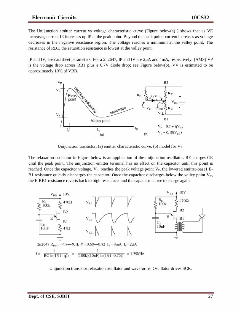
The Unijunction emitter current vs voltage characteristic curve (Figure below(a) ) shows that as VE
increases, current IE increases up IP at the peak point. Beyond the peak point, current increases as voltage
decreases in the negative resistance region. The voltage reaches a minimum at the valley point. The
resistance of RB1, the saturation resistance is lowest at the valley point.
IP and IV, are datasheet parameters; For a 2n2647, IP and IV are 2µA and 4mA, respectively. [AMS] VP
is the voltage drop across RB1 plus a 0.7V diode drop; see Figure below(b). VV is estimated to be
approximately 10% of VBB.
Unijunction transistor: (a) emitter characteristic curve, (b) model for VP .
The relaxation oscillator in Figure below is an application of the unijunction oscillator. RE charges CE
until the peak point. The unijunction emitter terminal has no effect on the capacitor until this point is
reached. Once the capacitor voltage, VE, reaches the peak voltage point VP, the lowered emitter-base1 E-
B1 resistance quickly discharges the capacitor. Once the capacitor discharges below the valley point VV,
the E-RB1 resistance reverts back to high resistance, and the capacitor is free to charge again.
Unijunction transistor relaxation oscillator and waveforms. Oscillator drives SCR.

Electronic Circuits 10CS32
Dept. of CSE, SJBIT 28
During capacitor discharge through the E-B1 saturation resistance, a pulse may be seen on the external B1
and B2 load resistors, Figure above. The load resistor at B1 needs to be low to not affect the discharge
time. The external resistor at B2 is optional. It may be replaced by a short circuit. The approximate
frequency is given by 1/f = T = RC. A more accurate expression for frequency is given in Figure above.
The charging resistor RE must fall within certain limits. It must be small enough to allow IP to flow based
on the VBB supply less VP. It must be large enough to supply IV based on the VBB supply less VV.
[MHW] The equations and an example for a 2n2647:
Programmable Unijunction Transistor (PUT): Although the unijunction transistor is listed as obsolete
(read expensive if obtainable), the programmable unijunction transistor is alive and well. It is inexpensive
and in production. Though it serves a function similar to the unijunction transistor, the PUT is a three
terminal thyristor. The PUT shares the four-layer structure typical of thyristors shown in Figure below.
Note that the gate, an N-type layer near the anode, is known as an “anode gate”. Moreover, the gate lead
on the schematic symbol is attached to the anode end of the symbol.
Programmable unijunction transistor: Characteristic curve, internal construction, schematic symbol.
The characteristic curve for the programmable unijunction transistor in Figure above is similar to that of
the unijunction transistor. This is a plot of anode current IA versus anode voltage VA. The gate lead
voltage sets, programs, the peak anode voltage VP. As anode current inceases, voltage increases up to the
peak point. Thereafter, increasing current results in decreasing voltage, down to the valley point.

Electronic Circuits 10CS32
Dept. of CSE, SJBIT 29
The PUT equivalent of the unijunction transistor is shown in Figure below. External PUT resistors R1 and
R2 replace unijunction transistor internal resistors RB1 and RB2, respectively. These resistors allow the
calculation of the intrinsic standoff ratio η.
PUT equivalent of unijunction transistor
Figure below shows the PUT version of the unijunction relaxation oscillator Figure previous. Resistor R
charges the capacitor until the peak point, Figure previous, then heavy conduction moves the operating
point down the negative resistance slope to the valley point. A current spike flows through the cathode
during capacitor discharge, developing a voltage spike across the cathode resistors. After capacitor
discharge, the operating point resets back to the slope up to the peak point.
PUT relaxation oscillator
Problem: What is the range of suitable values for R in Figure above, a relaxation oscillator? The charging
resistor must be small enough to supply enough current to raise the anode to VP the peak point (Figure
previous) while charging the capacitor. Once VP is reached, anode voltage decreases as current increases
(negative resistance), which moves the operating point to the valley. It is the job of the capacitor to supply
the valley current IV. Once it is discharged, the operating point resets back to the upward slope to the
peak point. The resistor must be large enough so that it will never supply the high valley current IP. If the
charging resistor ever could supply that much current, the resistor would supply the valley current after

Electronic Circuits 10CS32
Dept. of CSE, SJBIT 30
the capacitor was discharged and the operating point would never reset back to the high resistance
condition to the left of the peak point.
We select the same VBB=10V used for the unijunction transistor example. We select values of R1 and R2
so that η is about 2/3. We calculate η and VS. The parallel equivalent of R1, R2 is RG, which is only used
to make selections from Table below. Along with VS=10, the closest value to our 6.3, we find VT=0.6V,
in Table below and calculate VP.
We also find IP and IV, the peak and valley currents, respectively in Table below. We still need VV, the
valley voltage. We used 10% of VBB= 1V, in the previous unijunction example. Consulting the
datasheet, we find the forward voltage VF=0.8V at IF=50mA. The valley current IV=70µA is much less
than IF=50mA. Therefore, VV must be less than VF=0.8V. How much less? To be safe we set VV=0V.
This will raise the lower limit on the resistor range a little.
Choosing R > 143k guarantees that the operating point can reset from the valley point after capacitor
discharge. R < 755k allows charging up to VP at the peak point.
Figure below show the PUT relaxation oscillator with the final resistor values. A practical application of a
PUT triggering an SCR is also shown. This circuit needs a VBB unfiltered supply (not shown) divided
down from the bridge rectifier to reset the relaxation oscillator after each power zero crossing. The
variable resistor should have a minimum resistor in series with it to prevent a low pot setting from
hanging at the valley point.

Electronic Circuits 10CS32
Dept. of CSE, SJBIT 31
PUT relaxation oscillator with component values. PUT drives SCR lamp dimmer.
1.4 Silicon-Controlled Rectifiers, or SCRs
Shockley diodes are curious devices, but rather limited in application. Their usefulness may be expanded,
however, by equipping them with another means of latching. In doing so, each becomes true amplifying
devices (if only in an on/off mode), and we refer to these as silicon-controlled rectifiers, or SCRs.
The progression from Shockley diode to SCR is achieved with one small addition, actually nothing more
than a third wire connection to the existing PNPN structure: (Figure below)
The Silicon-Controlled Rectifier (SCR)
If an SCR's gate is left floating (disconnected), it behaves exactly as a Shockley diode. It may be latched
by break-over voltage or by exceeding the critical rate of voltage rise between anode and cathode, just as
with the Shockley diode. Dropout is accomplished by reducing current until one or both internal
transistors fall into cutoff mode, also like the Shockley diode. However, because the gate terminal
connects directly to the base of the lower transistor, it may be used as an alternative means to latch the
SCR. By applying a small voltage between gate and cathode, the lower transistor will be forced on by the
resulting base current, which will cause the upper transistor to conduct, which then supplies the lower
transistor's base with current so that it no longer needs to be activated by a gate voltage. The necessary
gate current to initiate latch-up, of course, will be much lower than the current through the SCR from
cathode to anode, so the SCR does achieve a measure of amplification.
Electronic Circuits 10CS32
Dept. of CSE, SJBIT 32
This method of securing SCR conduction is called triggering, and it is by far the most common way that
SCRs are latched in actual practice. In fact, SCRs are usually chosen so that their breakover voltage is far
beyond the greatest voltage expected to be experienced from the power source, so that it can be turned on
only by an intentional voltage pulse applied to the gate.
It should be mentioned that SCRs may sometimes be turned off by directly shorting their gate and cathode
terminals together, or by "reverse-triggering" the gate with a negative voltage (in reference to the
cathode), so that the lower transistor is forced into cutoff. I say this is "sometimes" possible because it
involves shunting all of the upper transistor's collector current past the lower transistor's base. This
current may be substantial, making triggered shut-off of an SCR difficult at best. A variation of the SCR,
called a Gate-Turn-Off thyristor, or GTO, makes this task easier. But even with a GTO, the gate current
required to turn it off may be as much as 20% of the anode (load) current! The schematic symbol for a
GTO is shown in the following illustration: (Figure below)
1.5 The Gate Turn-Off Thyristors (GTO)
SCRs and GTOs share the same equivalent schematics (two transistors connected in a positive-feedback
fashion), the only differences being details of construction designed to grant the NPN transistor a greater
β than the PNP. This allows a smaller gate current (forward or reverse) to exert a greater degree of control
over conduction from cathode to anode, with the PNP transistor's latched state being more dependent
upon the NPN's than vice versa. The Gate-Turn-Off thyristor is also known by the name of Gate-
Controlled Switch, or GCS.
A rudimentary test of SCR function, or at least terminal identification, may be performed with an
ohmmeter. Because the internal connection between gate and cathode is a single PN junction, a meter
should indicate continuity between these terminals with the red test lead on the gate and the black test
lead on the cathode like this: (Figure below)

Electronic Circuits 10CS32
Dept. of CSE, SJBIT 33
Rudimentary test of SCR
All other continuity measurements performed on an SCR will show "open" ("OL" on some digital
multimeter displays). It must be understood that this test is very crude and does not constitute a
comprehensive assessment of the SCR. It is possible for an SCR to give good ohmmeter indications and
still be defective. Ultimately, the only way to test an SCR is to subject it to a load current.
If you are using a multimeter with a "diode check" function, the gate-to-cathode junction voltage
indication you get may or may not correspond to what's expected of a silicon PN junction (approximately
0.7 volts). In some cases, you will read a much lower junction voltage: mere hundredths of a volt. This is
due to an internal resistor connected between the gate and cathode incorporated within some SCRs. This
resistor is added to make the SCR less susceptible to false triggering by spurious voltage spikes, from
circuit "noise" or from static electric discharge. In other words, having a resistor connected across the
gate-cathode junction requires that a strong triggering signal (substantial current) be applied to latch the
SCR. This feature is often found in larger SCRs, not on small SCRs. Bear in mind that an SCR with an
internal resistor connected between gate and cathode will indicate continuity in both directions between
those two terminals: (Figure below)
Larger SCRs have gate to cathode resistor.
"Normal" SCRs, lacking this internal resistor, are sometimes referred to as sensitive gate SCRs due to
their ability to be triggered by the slightest positive gate signal.
The test circuit for an SCR is both practical as a diagnostic tool for checking suspected SCRs and also an
excellent aid to understanding basic SCR operation. A DC voltage source is used for powering the circuit,
and two pushbutton switches are used to latch and unlatch the SCR, respectively: (Figure below)

Electronic Circuits 10CS32
Dept. of CSE, SJBIT 34
SCR testing circuit
Actuating the normally-open "on" pushbutton switch connects the gate to the anode, allowing current
from the negative terminal of the battery, through the cathode-gate PN junction, through the switch,
through the load resistor, and back to the battery. This gate current should force the SCR to latch on,
allowing current to go directly from cathode to anode without further triggering through the gate. When
the "on" pushbutton is released, the load should remain energized.
Pushing the normally-closed "off" pushbutton switch breaks the circuit, forcing current through the SCR
to halt, thus forcing it to turn off (low-current dropout).
If the SCR fails to latch, the problem may be with the load and not the SCR. A certain minimum amount
of load current is required to hold the SCR latched in the "on" state. This minimum current level is called
the holding current. A load with too great a resistance value may not draw enough current to keep an SCR
latched when gate current ceases, thus giving the false impression of a bad (unlatchable) SCR in the test
circuit. Holding current values for different SCRs should be available from the manufacturers. Typical
holding current values range from 1 milliamp to 50 milliamps or more for larger units.
For the test to be fully comprehensive, more than the triggering action needs to be tested. The forward
breakover voltage limit of the SCR could be tested by increasing the DC voltage supply (with no
pushbuttons actuated) until the SCR latches all on its own. Beware that a breakover test may require very
high voltage: many power SCRs have breakover voltage ratings of 600 volts or more! Also, if a pulse
voltage generator is available, the critical rate of voltage rise for the SCR could be tested in the same way:
subject it to pulsing supply voltages of different V/time rates with no pushbutton switches actuated and
see when it latches.
In this simple form, the SCR test circuit could suffice as a start/stop control circuit for a DC motor, lamp,
or other practical load: (Figure below)

Electronic Circuits 10CS32
Dept. of CSE, SJBIT 35
DC motor start/stop control circuit
Another practical use for the SCR in a DC circuit is as a crowbar device for overvoltage protection. A
"crowbar" circuit consists of an SCR placed in parallel with the output of a DC power supply, for placing
a direct short-circuit on the output of that supply to prevent excessive voltage from reaching the load.
Damage to the SCR and power supply is prevented by the judicious placement of a fuse or substantial
series resistance ahead of the SCR to limit short-circuit current: (Figure below)
Crowbar circuit used in DC power supply
Some device or circuit sensing the output voltage will be connected to the gate of the SCR, so that when
an overvoltage condition occurs, voltage will be applied between the gate and cathode, triggering the SCR
and forcing the fuse to blow. The effect will be approximately the same as dropping a solid steel crowbar
directly across the output terminals of the power supply, hence the name of the circuit.
Most applications of the SCR are for AC power control, despite the fact that SCRs are inherently DC
(unidirectional) devices. If bidirectional circuit current is required, multiple SCRs may be used, with one
or more facing each direction to handle current through both half-cycles of the AC wave. The primary
reason SCRs are used at all for AC power control applications is the unique response of a thyristor to an
alternating current. As we saw, the thyratron tube (the electron tube version of the SCR) and the DIAC, a
hysteretic device triggered on during a portion of an AC half-cycle will latch and remain on throughout
the remainder of the half-cycle until the AC current decreases to zero, as it must to begin the next half-
cycle. Just prior to the zero-crossover point of the current waveform, the thyristor will turn off due to
insufficient current (this behavior is also known as natural commutation) and must be fired again during
the next cycle. The result is a circuit current equivalent to a "chopped up" sine wave. For review, here is

Electronic Circuits 10CS32
Dept. of CSE, SJBIT 36
the graph of a DIAC's response to an AC voltage whose peak exceeds the breakover voltage of the DIAC:
(Figure below)
DIAC bidirectional response
With the DIAC, that breakover voltage limit was a fixed quantity. With the SCR, we have control over
exactly when the device becomes latched by triggering the gate at any point in time along the waveform.
By connecting a suitable control circuit to the gate of an SCR, we can "chop" the sine wave at any point
to allow for time-proportioned power control to a load.
Take the circuit in Figure below as an example. Here, an SCR is positioned in a circuit to control power to
a load from an AC source.
SCR control of AC power
Being a unidirectional (one-way) device, at most we can only deliver half-wave power to the load, in the
half-cycle of AC where the supply voltage polarity is positive on the top and negative on the bottom.
However, for demonstrating the basic concept of time-proportional control, this simple circuit is better
than one controlling full-wave power (which would require two SCRs).
With no triggering to the gate, and the AC source voltage well below the SCR's breakover voltage rating,
the SCR will never turn on. Connecting the SCR gate to the anode through a standard rectifying diode (to
prevent reverse current through the gate in the event of the SCR containing a built-in gate-cathode
resistor), will allow the SCR to be triggered almost immediately at the beginning of every positive half-
cycle: (Figure below)

Electronic Circuits 10CS32
Dept. of CSE, SJBIT 37
Gate connected directly to anode through a diode; nearly complete half-wave current through load.
We can delay the triggering of the SCR, however, by inserting some resistance into the gate circuit, thus
increasing the amount of voltage drop required before enough gate current triggers the SCR. In other
words, if we make it harder for electrons to flow through the gate by adding a resistance, the AC voltage
will have to reach a higher point in its cycle before there will be enough gate current to turn the SCR on.
The result is in Figure below.
Resistance inserted in gate circuit; less than half-wave current through load.
With the half-sine wave chopped up to a greater degree by delayed triggering of the SCR, the load
receives less average power (power is delivered for less time throughout a cycle). By making the series
gate resistor variable, we can make adjustments to the time-proportioned power: (Figure below)

Electronic Circuits 10CS32
Dept. of CSE, SJBIT 38
Increasing the resistance raises the threshold level, causing less power to be delivered to the load.
Decreasing the resistance lowers the threshold level, causing more power to be delivered to the load.
Unfortunately, this control scheme has a significant limitation. In using the AC source waveform for our
SCR triggering signal, we limit control to the first half of the waveform's half-cycle. In other words, it is
not possible for us to wait until after the wave's peak to trigger the SCR. This means we can turn down
the power only to the point where the SCR turns on at the very peak of the wave: (Figure below)
Circuit at minimum power setting
Raising the trigger threshold any more will cause the circuit to not trigger at all, since not even the peak
of the AC power voltage will be enough to trigger the SCR. The result will be no power to the load.
An ingenious solution to this control dilemma is found in the addition of a phase-shifting capacitor to the
circuit: (Figure below)

Electronic Circuits 10CS32
Dept. of CSE, SJBIT 39
Addition of a phase-shifting capacitor to the circuit
The smaller waveform shown on the graph is voltage across the capacitor. For the sake of illustrating the
phase shift, I'm assuming a condition of maximum control resistance where the SCR is not triggering at
all with no load current, save for what little current goes through the control resistor and capacitor. This
capacitor voltage will be phase-shifted anywhere from 0o to 90
o lagging behind the power source AC
waveform. When this phase-shifted voltage reaches a high enough level, the SCR will trigger.
With enough voltage across the capacitor to periodically trigger the SCR, the resulting load current
waveform will look something like Figure below)
Phase-shifted signal triggers SCR into conduction.
Because the capacitor waveform is still rising after the main AC power waveform has reached its peak, it
becomes possible to trigger the SCR at a threshold level beyond that peak, thus chopping the load current
wave further than it was possible with the simpler circuit. In reality, the capacitor voltage waveform is a
bit more complex that what is shown here, its sinusoidal shape distorted every time the SCR latches on.
However, what I'm trying to illustrate here is the delayed triggering action gained with the phase-shifting
RC network; thus, a simplified, undistorted waveform serves the purpose well.
SCRs may also be triggered, or "fired," by more complex circuits. While the circuit previously shown is
sufficient for a simple application like a lamp control, large industrial motor controls often rely on more
sophisticated triggering methods. Sometimes, pulse transformers are used to couple a triggering circuit to
the gate and cathode of an SCR to provide electrical isolation between the triggering and power circuits:
(Figure below)
Transformer coupling of trigger signal provides isolation.

Electronic Circuits 10CS32
Dept. of CSE, SJBIT 40
When multiple SCRs are used to control power, their cathodes are often not electrically common, making
it difficult to connect a single triggering circuit to all SCRs equally. An example of this is the controlled
bridge rectifier shown in Figure below.
Controlled bridge rectifier
In any bridge rectifier circuit, the rectifying diodes (in this example, the rectifying SCRs) must conduct in
opposite pairs. SCR1 and SCR3 must be fired simultaneously, and SCR2 and SCR4 must be fired together
as a pair. As you will notice, though, these pairs of SCRs do not share the same cathode connections,
meaning that it would not work to simply parallel their respective gate connections and connect a single
voltage source to trigger both: (Figure below)
This strategy will not work for triggering SCR2 and SCR4 as a pair.
Although the triggering voltage source shown will trigger SCR4, it will not trigger SCR2 properly because
the two thyristors do not share a common cathode connection to reference that triggering voltage. Pulse
transformers connecting the two thyristor gates to a common triggering voltage source will work,
however: (Figure below)

Electronic Circuits 10CS32
Dept. of CSE, SJBIT 41
Transformer coupling of the gates allows triggering of SCR2 and SCR4 .
Bear in mind that this circuit only shows the gate connections for two out of the four SCRs. Pulse
transformers and triggering sources for SCR1 and SCR3, as well as the details of the pulse sources
themselves, have been omitted for the sake of simplicity.
Controlled bridge rectifiers are not limited to single-phase designs. In most industrial control systems, AC
power is available in three-phase form for maximum efficiency, and solid-state control circuits are built to
take advantage of that. A three-phase controlled rectifier circuit built with SCRs, without pulse
transformers or triggering circuitry shown, would look like Figure below.
Three-phase bridge SCR control of load
1.6 Recommended Questions
1. Explain the clipping above and below the reference voltage in a basic parallel clipper.
2. Explain the clipping above and below the reference voltage in the basic series clipper.
3. Explain the clippers with voltage divider circuit.
4. Explain the negative & positive clamper circuit.
5. Draw and explain the characteristics of Schottky diode.
6. What is feature of a Varactor diode?
7. What is a voltage multiplier circuit? Explain the operation of a full wave voltage doubler
circuit. (Jan-2007)
8. Define diffusion capacitance. Derive an expression for the same. (July-2007)
9. Draw the piece wise linear V-I characteristics of a P-N junction diode. Give the circuit
model for the ON state and OFF state. (July-2007)

Electronic Circuits 10CS32
Dept. of CSE, SJBIT 42
10. Discuss voltage doubler circuit. (Jan-2008)
11. Define regulation and derive equation for a full wave circuit. (Jan-2008)

Electronic Circuits 10CS32
Dept. of CSE, SJBIT 43
Unit – 2: Bipolar Junction Transistors
2.1 Bipolar junction transistor (BJT)
The bipolar junction transistor (BJT) was the first solid-state amplifier element and started the
solid-state electronics revolution. Bardeen, Brattain and Shockley, while at Bell Laboratories,
invented it in 1948 as part of a post-war effort to replace vacuum tubes with solid-state devices.
Solid-state rectifiers were already in use at the time and were preferred over vacuum diodes
because of their smaller size, lower weight and higher reliability. A solid-state replacement for a
vacuum triode was expected to yield similar advantages. The work at Bell Laboratories was
highly successful and culminated in Bardeen, Brattain and Shockley receiving the Nobel Prize in
1956.
Their work led them first to the point-contact transistor and then to the bipolar junction
transistor. They used germanium as the semiconductor of choice because it was possible to
obtain high purity material. The extraordinarily large diffusion length of minority carriers in
germanium provided functional structures despite the large dimensions of the early devices.
Since then, the technology has progressed rapidly. The development of a planar process yielded
the first circuits on a chip and for a decade, bipolar transistor operational amplifiers, like the 741,
and digital TTL circuits were for a long time the workhorses of any circuit designer.
The spectacular rise of the MOSFET market share during the last decade has completely
removed the bipolar transistor from center stage. Almost all logic circuits, microprocessor and
memory chips contain exclusively MOSFETs.
Nevertheless, bipolar transistors remain important devices for ultra-high-speed discrete logic
circuits such as emitter coupled logic (ECL), power-switching applications and in microwave
power amplifiers. Heterojunction bipolar transistors (HBTs) have emerged as the device of
choice for cell phone amplifiers and other demanding applications.
In this chapter we first present the structure of the bipolar transistor and show how a three-layer
structure with alternating n-type and p-type regions can provide current and voltage
amplification. We then present the ideal transistor model and derive an expression for the current
gain in the forward active mode of operation. Next, we discuss the non-ideal effects, the
modulation of the base width and recombination in the depletion region of the base-emitter
junction. A discussion of transit time effects, BJT circuit models, HBTs, BJT technology and
bipolar power devices completes this chapter.
Structure and principle of operation
A bipolar junction transistor consists of two back-to-back p-n junctions, who share a thin
common region with width, wB. Contacts are made to all three regions, the two outer regions
called the emitter and collector and the middle region called the base. The structure of an npn

Electronic Circuits 10CS32
Dept. of CSE, SJBIT 44
bipolar transistor is shown in Figure (a). The device is called “bipolar” since its operation
involves both types of mobile carriers, electrons and holes.
Figure 5.2.1: (a) Structure and sign convention of a npn bipolar junction transistor. (b) Electron
and hole flow under forward active bias, VBE > 0 and VBC = 0.
Since the device consists of two back-to-back diodes, there are depletion regions between the
quasi-neutral regions. The width of the quasi neutral regions in the emitter, base and collector are
indicated with the symbols wE', wB
' and wC
' and are calculated from

Electronic Circuits 10CS32
Dept. of CSE, SJBIT 45
where the depletion region widths are given by:
With
The sign convention of the currents and voltage is indicated on Figure 5.2.1(a). The base and
collector current are positive if a positive current goes into the base or collector contact. The
emitter current is positive for a current coming out of the emitter contact. This also implies that
the emitter current, IE, equals the sum of the base current, IB, and the collector current, IC:
The base-emitter voltage and the base-collector voltage are positive if a positive voltage is
applied to the base contact relative to the emitter and collector respectively.
The operation of the device is illustrated with Figure 5.2.1 (b). We consider here only the
forward active bias mode of operation, obtained by forward biasing the base-emitter junction and
reverse biasing the base-collector junction. To simplify the discussion further, we also set VCE =
0. The corresponding energy band diagram is shown in Figure 5.2.2. Electrons diffuse from the

Electronic Circuits 10CS32
Dept. of CSE, SJBIT 46
emitter into the base and holes diffuse from the base into the emitter. This carrier diffusion is
identical to that in a p-n junction. However, what is different is that the electrons can diffuse as
minority carriers through the quasi-neutral base. Once the electrons arrive at the base-collector
depletion region, they are swept through the depletion layer due to the electric field. These
electrons contribute to the collector current. In addition, there are two more currents, the base
recombination current, indicated on Figure 5.2.2 by the vertical arrow, and the base-emitter
depletion layer recombination current, Ir,d, (not shown).
Figure 5.2.2. : Energy band diagram of a bipolar transistor biased in the forward active mode.
The total emitter current is the sum of the electron diffusion current, IE,n, the hole diffusion
current, IE,p and the base-emitter depletion layer recombination current, Ir,d.
The total collector current is the electron diffusion current, IE,n, minus the base recombination
current, Ir,B.
The base current is the sum of the hole diffusion current, IE,p, the base recombination current, Ir,B
and the base-emitter depletion layer recombination current, Ir,d.
The transport factor, is defined as the ratio of the collector and emitter current:

Electronic Circuits 10CS32
Dept. of CSE, SJBIT 47
Using Kirchoff‟s current law and the sign convention shown in Figure 5.2.1(a), we find that the
base current equals the difference between the emitter and collector current. The current gain, is
defined as the ratio of the collector and base current and equals:
This explains how a bipolar junction transistor can provide current amplification. If the collector
current is almost equal to the emitter current, the transport factor, , approaches one. The current
gain, , can therefore become much larger than one.
To facilitate further analysis, we now rewrite the transport factor, , as the product of the emitter
efficiency, E, the base transport factor, T, and the depletion layer recombination factor, r.
The emitter efficiency, E, is defined as the ratio of the electron current in the emitter, IE,n, to the
sum of the electron and hole current diffusing across the base-emitter junction, IE,n + IE,p.
The base transport factor, T, equals the ratio of the current due to electrons injected in the
collector, to the current due to electrons injected in the base.
Recombination in the depletion-region of the base-emitter junction further reduces the current
gain, as it increases the emitter current without increasing the collector current. The depletion
layer recombination factor, r, equals the ratio of the current due to electron and hole diffusion
across the base-emitter junction to the total emitter current:

Electronic Circuits 10CS32
Dept. of CSE, SJBIT 48
Example 5.1 A bipolar transistor with an emitter current of 1 mA has an emitter efficiency of
0.99, a base transport factor of 0.995 and a depletion layer recombination factor of 0.998.
Calculate the base current, the collector current, the transport factor and the current gain of the
transistor.
Solution: The transport factor and current gain are:
and
The collector current then equals
And the base current is obtained from:
2.2 The Field Effect Transistor
In the Bipolar Junction Transistor tutorials, we saw that the output Collector current of the
transistor is proportional to input current flowing into the Base terminal of the device, thereby
making the bipolar transistor a "CURRENT" operated device (Beta model). The Field Effect
Transistor, or simply FET however, uses the voltage that is applied to their input terminal,
called the Gate to control the current flowing through them resulting in the output current being
proportional to the input voltage. As their operation relies on an electric field (hence the name
field effect) generated by the input Gate voltage, this then makes the Field Effect Transistor a
"VOLTAGE" operated device.

Electronic Circuits 10CS32
Dept. of CSE, SJBIT 49
Typical Field Effect Transistor
The Field Effect Transistor is a three terminal unipolar semiconductor device that has very
similar characteristics to those of their Bipolar Transistor counterparts ie, high efficiency, instant
operation, robust and cheap and can be used in most electronic circuit applications to replace
their equivalent bipolar junction transistors (BJT) cousins.
Field effect transistors can be made much smaller than an equivalent BJT transistor and along
with their low power consumption and power dissipation makes them ideal for use in integrated
circuits such as the CMOS range of digital logic chips.
We remember from the previous tutorials that there are two basic types of Bipolar Transistor
construction, NPN and PNP, which basically describes the physical arrangement of the P-type
and N-type semiconductor materials from which they are made. This is also true of FET's as
there are also two basic classifications of Field Effect Transistor, called the N-channel FET and
the P-channel FET.
The field effect transistor is a three terminal device that is constructed with no PN-junctions
within the main current carrying path between the Drain and the Source terminals, which
correspond in function to the Collector and the Emitter respectively of the bipolar transistor. The
current path between these two terminals is called the "channel" which may be made of either a
P-type or an N-type semiconductor material. The control of current flowing in this channel is
achieved by varying the voltage applied to the Gate. As their name implies, Bipolar Transistors
are "Bipolar" devices because they operate with both types of charge carriers, Holes and
Electrons. The Field Effect Transistor on the other hand is a "Unipolar" device that depends only
on the conduction of electrons (N-channel) or holes (P-channel).
The Field Effect Transistor has one major advantage over its standard bipolar transistor
cousins, in that their input impedance, ( Rin ) is very high, (thousands of Ohms), while the BJT is
comparatively low. This very high input impedance makes them very sensitive to input voltage
signals, but the price of this high sensitivity also means that they can be easily damaged by static
electricity. There are two main types of field effect transistor, the Junction Field Effect
Transistor or JFET and the Insulated-gate Field Effect Transistor or IGFET), which is more
commonly known as the standard Metal Oxide Semiconductor Field Effect Transistor or
MOSFET for short.

Electronic Circuits 10CS32
Dept. of CSE, SJBIT 50
2.3 The Junction Field Effect Transistor
We saw previously that a bipolar junction transistor is constructed using two PN-junctions in the
main current carrying path between the Emitter and the Collector terminals. The Junction Field
Effect Transistor (JUGFET or JFET) has no PN-junctions but instead has a narrow piece of
high-resistivity semiconductor material forming a "Channel" of either N-type or P-type silicon
for the majority carriers to flow through with two ohmic electrical connections at either end
commonly called the Drain and the Source respectively.
There are two basic configurations of junction field effect transistor, the N-channel JFET and the
P-channel JFET. The N-channel JFET's channel is doped with donor impurities meaning that the
flow of current through the channel is negative (hence the term N-channel) in the form of
electrons. Likewise, the P-channel JFET's channel is doped with acceptor impurities meaning
that the flow of current through the channel is positive (hence the term P-channel) in the form of
holes. N-channel JFET's have a greater channel conductivity (lower resistance) than their
equivalent P-channel types, since electrons have a higher mobility through a conductor compared
to holes. This makes the N-channel JFET's a more efficient conductor compared to their P-
channel counterparts.
We have said previously that there are two ohmic electrical connections at either end of the
channel called the Drain and the Source. But within this channel there is a third electrical
connection which is called the Gate terminal and this can also be a P-type or N-type material
forming a PN-junction with the main channel. The relationship between the connections of a
junction field effect transistor and a bipolar junction transistor are compared below.
2.4 Comparison of connections between a JFET and a BJT
Bipolar Transistor Field Effect Transistor
Emitter - (E) >> Source - (S)
Base - (B) >> Gate - (G)
Collector - (C) >> Drain - (D)
The symbols and basic construction for both configurations of JFETs are shown below.

Electronic Circuits 10CS32
Dept. of CSE, SJBIT 51
The semiconductor "channel" of the Junction Field Effect Transistor is a resistive path through
which a voltage VDS causes a current ID to flow. The JFET can conduct current equally well in
either direction. A voltage gradient is thus formed down the length of the channel with this
voltage becoming less positive as we go from the Drain terminal to the Source terminal. The PN-
junction therefore has a high reverse bias at the Drain terminal and a lower reverse bias at the
Source terminal. This bias causes a "depletion layer" to be formed within the channel and whose
width increases with the bias.
The magnitude of the current flowing through the channel between the Drain and the Source
terminals is controlled by a voltage applied to the Gate terminal, which is a reverse-biased. In an
N-channel JFET this Gate voltage is negative while for a P-channel JFET the Gate voltage is
positive. The main difference between the JFET and a BJT device is that when the JFET junction
is reverse-biased the Gate current is practically zero, whereas the Base current of the BJT is
always some value greater than zero.
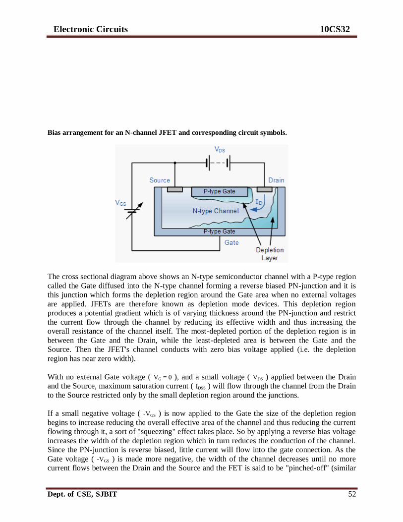
Electronic Circuits 10CS32
Dept. of CSE, SJBIT 52
Bias arrangement for an N-channel JFET and corresponding circuit symbols.
The cross sectional diagram above shows an N-type semiconductor channel with a P-type region
called the Gate diffused into the N-type channel forming a reverse biased PN-junction and it is
this junction which forms the depletion region around the Gate area when no external voltages
are applied. JFETs are therefore known as depletion mode devices. This depletion region
produces a potential gradient which is of varying thickness around the PN-junction and restrict
the current flow through the channel by reducing its effective width and thus increasing the
overall resistance of the channel itself. The most-depleted portion of the depletion region is in
between the Gate and the Drain, while the least-depleted area is between the Gate and the
Source. Then the JFET's channel conducts with zero bias voltage applied (i.e. the depletion
region has near zero width).
With no external Gate voltage ( VG = 0 ), and a small voltage ( VDS ) applied between the Drain
and the Source, maximum saturation current ( IDSS ) will flow through the channel from the Drain
to the Source restricted only by the small depletion region around the junctions.
If a small negative voltage ( -VGS ) is now applied to the Gate the size of the depletion region
begins to increase reducing the overall effective area of the channel and thus reducing the current
flowing through it, a sort of "squeezing" effect takes place. So by applying a reverse bias voltage
increases the width of the depletion region which in turn reduces the conduction of the channel.
Since the PN-junction is reverse biased, little current will flow into the gate connection. As the
Gate voltage ( -VGS ) is made more negative, the width of the channel decreases until no more
current flows between the Drain and the Source and the FET is said to be "pinched-off" (similar

Electronic Circuits 10CS32
Dept. of CSE, SJBIT 53
to the cut-off region for a BJT). The voltage at which the channel closes is called the "pinch-off
voltage", ( VP ).
JFET Channel Pinched-off
In this pinch-off region the Gate voltage, VGS controls the channel current and VDS has little or no effect.
JFET Model
The result is that the FET acts more like a voltage controlled resistor which has zero resistance when
VGS = 0 and maximum "ON" resistance ( RDS ) when the Gate voltage is very negative. Under normal
operating conditions, the JFET gate is always negatively biased relative to the source.
It is essential that the Gate voltage is never positive since if it is all the channel current will flow
to the Gate and not to the Source, the result is damage to the JFET. Then to close the channel:
No Gate voltage ( VGS ) and VDS is increased from zero.
No VDS and Gate control is decreased negatively from zero.
VDS and VGS varying.
The P-channel Junction Field Effect Transistor operates the same as the N-channel above, with
the following exceptions: 1). Channel current is positive due to holes, 2). The polarity of the
biasing voltage needs to be reversed.
The output characteristics of an N-channel JFET with the gate short-circuited to the source is
given as
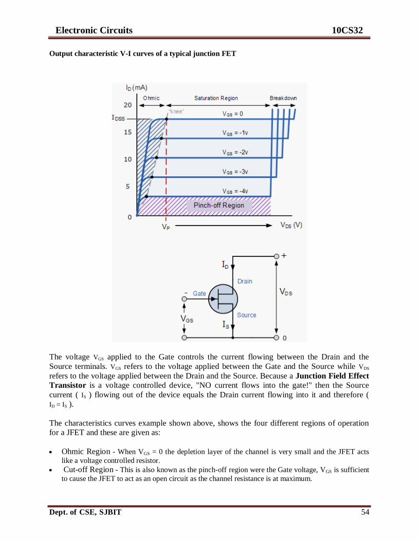
Electronic Circuits 10CS32
Dept. of CSE, SJBIT 54
Output characteristic V-I curves of a typical junction FET
The voltage VGS applied to the Gate controls the current flowing between the Drain and the
Source terminals. VGS refers to the voltage applied between the Gate and the Source while VDS
refers to the voltage applied between the Drain and the Source. Because a Junction Field Effect
Transistor is a voltage controlled device, "NO current flows into the gate!" then the Source
current ( IS ) flowing out of the device equals the Drain current flowing into it and therefore (
ID = IS ).
The characteristics curves example shown above, shows the four different regions of operation
for a JFET and these are given as:
Ohmic Region - When VGS = 0 the depletion layer of the channel is very small and the JFET acts
like a voltage controlled resistor.
Cut-off Region - This is also known as the pinch-off region were the Gate voltage, VGS is sufficient
to cause the JFET to act as an open circuit as the channel resistance is at maximum.

Electronic Circuits 10CS32
Dept. of CSE, SJBIT 55
Saturation or Active Region - The JFET becomes a good conductor and is controlled by the Gate-
Source voltage, ( VGS ) while the Drain-Source voltage, ( VDS ) has little or no effect.
Breakdown Region - The voltage between the Drain and the Source, ( VDS ) is high enough to
causes the JFET's resistive channel to break down and pass uncontrolled maximum current.
The characteristics curves for a P-channel junction field effect transistor are the same as those
above, except that the Drain current ID decreases with an increasing positive Gate-Source
voltage, VGS.
The Drain current is zero when VGS = VP. For normal operation, VGS is biased to be somewhere
between VP and 0. Then we can calculate the Drain current, ID for any given bias point in the
saturation or active region as follows:
Drain current in the active region.
Note that the value of the Drain current will be between zero (pinch-off) and IDSS (maximum
current). By knowing the Drain current ID and the Drain-Source voltage VDS the resistance of the
channel ( ID ) is given as:
Drain-Source channel resistance.
Where: gm is the "transconductance gain" since the JFET is a voltage controlled device and which
represents the rate of change of the Drain current with respect to the change in Gate-Source
voltage.
2.5 JFET Amplifier
Just like the bipolar junction transistor, JFET's can be used to make single stage class A amplifier
circuits with the JFET common source amplifier and characteristics being very similar to the BJT
common emitter circuit. The main advantage JFET amplifiers have over BJT amplifiers is their
high input impedance which is controlled by the Gate biasing resistive network formed by R1 and
R2 as shown.

Electronic Circuits 10CS32
Dept. of CSE, SJBIT 56
Biasing of JFET Amplifier
This common source (CS) amplifier circuit is biased in class A mode by the voltage divider
network formed by R1 and R2. The voltage across the Source resistor RS is generally set at one
fourth VDD, ( VDD /4 ). The required Gate voltage can then be calculated using this RS value. Since
the Gate current is zero, ( IG = 0 ) we can set the required DC quiescent voltage by the proper
selection of resistors R1 and R2.
The control of the Drain current by a negative Gate potential makes the Junction Field Effect
Transistor useful as a switch and it is essential that the Gate voltage is never positive for an N-
channel JFET as the channel current will flow to the Gate and not the Drain resulting in damage
to the JFET. The principals of operation for a P-channel JFET are the same as for the N-channel
JFET, except that the polarity of the voltages need to be reversed.
In the next tutorial about Transistors, we will look at another type of Field Effect Transistor
called a MOSFET whose Gate connection is completely isolated from the main current carrying
channel.
2.6 CMOS
Complementary Metal-Oxide-Silicon circuits require an nMOS and pMOS transistor technology
on the same substrate. To this end, an n-type well is provided in the p-type substrate.
Alternatively one can use a p-well or both an n-type and p-type well in a low-doped substrate.
The gate oxide, poly-silicon gate and source-drain contact metal are typically shared between the
pMOS and nMOS technology, while the source-drain implants must be done separately. Since
CMOS circuits contain pMOS devices, which are affected by the lower hole mobility, CMOS
circuits are not faster than their all-nMOS counter parts. Even when scaling the size of the pMOS
devices so that they provide the same current, the larger pMOS device has a higher capacitance.
The CMOS advantage is that the output of a CMOS inverter can be as high as the power supply
voltage and as low as ground. This large voltage swing and the steep transition between logic
levels yield large operation margins and therefore also a high circuit yield. In addition, there is
no power dissipation in either logic state. Instead the power dissipation occurs only when a

Electronic Circuits 10CS32
Dept. of CSE, SJBIT 57
transition is made between logic states. CMOS circuits are therefore not faster than nMOS
circuits but are more suited for very/ultra large-scale integration (VLSI/ULSI).
CMOS circuits have one property, which is very undesirable, namely latchup. Latchup occurs
when four alternating p-type and n-type regions are brought in close proximity. Together they
form two bipolar transistors, one npn and one pnp transistor. The base of each transistor is
connected to the collector of the other, forming a cross-coupled thyristor-like combination. As a
current is applied to the base of one transistor, the current is amplified by the transistor and
provided as the base current of the other one. If the product of the current gain of both transistors
is larger than unity, the current through both devices increases until the series resistances of the
circuit limits the current. Latchup therefore results in excessive power dissipation and faulty
logic levels in the gates affected. In principle, this effect can be eliminated by separating the n-
type and p-type device. A more effective and less space-consuming solution is the use of
trenches, which block the minority carrier flow. A deep and narrow trench is etched between all
n-type and p-type wells, passivated and refilled with an insulating layer.
VMOS Transistors and UMOS
The VMOS transistor, named after the V-shaped groove, is a vertical MOSFET with high current
handling capability as well as high blocking voltage. It consists of a double diffused n+/p layer,
which is cut by a V-shaped groove. The V-groove is easily fabricated by anisotropically etching
a (100) silicon surface using a concentrated KOH solution. The V-groove is then coated with a
gate oxide, followed by the gate electrode. As the V-groove cuts through the double diffused
layer, it creates two vertical MOSFETs, one on each side of the groove. The combination of the
V-groove with the double diffused layers results in a short gate length, which is determined by
the thickness of the p-type layer. The vertical structure allows the use of a low-doped drain
region, which results in a high blocking voltage.
Figure: Insulated Gate Bipolar Transistor (IGBT): a) equivalent circuit and b) device cross-section.

Electronic Circuits 10CS32
Dept. of CSE, SJBIT 58
2.7 Recommended Questions
1. Draw and explain the base biased amplifier. 2. Draw a typical common emitter amplifier and explain the function of each component in it.
3. Explain the single stage CE amplifier.
4. Draw the dc and ac equivalent circuits for base bias, voltage divider and two supply emitter bias transistor circuits.
5. For the VBD amplifier shown below, draw the DC equivalent circuit and find the
6. DC quantities IE, VE, VCE and VC. (Jul-2009)
7. Explain with a neat circuit diagram and a.c equivalent circuit, the working of base biased
amplifier. (Jan-2010)
8. Sketch the output waveform for the clipper circuit of Fig.Q2 (b) shown below.
9. Assume silicon diode and obtain the peak magnitude of the output waveform.
(Jan-2010)
10. Find the voltage gain and output voltage across the load resistor for the given circuit of
FigQ2( C ) (Jan-2010)
11. Explain with a neat circuit diagram, voltage divider bias amplifier by mentioning the
importance of bypass capacitor. (Jun-2010)

Electronic Circuits 10CS32
Dept. of CSE, SJBIT 59
Unit – 3: Photodiodes
3.1 Photodiodes
Photodiodes are junction semiconductor light sensors that generate current or voltage when the PN
junction in the semiconductor is illuminated by light of sufficient energy.
The spectral response of the photodiode is a function of the bandgap energy of the material used in its
construction. The cut-off wavelength of the photodiode is given by
(eV) energy bandgap the is
(nm) wavelength off-cut the where
1240
g
c
gc E
is
E
Photodiodes are mostly constructed using silicon, germanium, indium gallium arsenide (InGaAs), lead
sulphide (Pbs) and mercury cadmium telluride (HgCdTe). Depending upon their construction there are
several types of photodiodes. They are,
3.2 PN Photodiode
PN Photodiodes comprise a PN junction as shown in figure.
When light with sufficient energy strikes the diode, photo-induced carriers are generated which include
electrons in the conduction band of the P-type material and holes in the valence band of the N-type
material.

Electronic Circuits 10CS32
Dept. of CSE, SJBIT 60
PN Photodiode Generation of current in a PN Photodiode
When photodiode is reverse biased, the photo-induced electrons will move down the potential hill from P-
side to the N-side. Similarly, the photo-induced holes will add to the current flow by moving across the
junction to the P-side from the N-side.
PN Photodiodes are used for precision photometry applications like medical instrumentation, analytical
instruments, semiconductor tools and industrial measurement systems.
3.3 PIN Photodiode
In PIN photodiodes, an extra high resistance intrinsic layer is added between the P and N layers. This has
the effect of reducing the transit or diffusion time of the photo-induced electron-hole pairs which in turn
results in improved response time.
PIN Photodiode
PIN photodiodes feature low capacitance, thereby offering high bandwidth making them suitable for high
speed photometry and optical communication applications.
3.4 Schottky Photodiode
In Schottky-type Photodiodes, a thin gold coating is sputtered onto the N-material to forma Schottky
effect PN junction. Schottky Photodiodes have enhanced ultraviolet (UV) response.
Avalanche Photodiode (APD)
APDs are high-speed, high-sensitivity photodiodes utilizing an internal gain mechanism that functions by
applying a relatively higher reverse bias voltage than that is applied in the case of PIN photodiodes.
APDs are so constructed to provide a very uniform junction that exhibits the avalanche effect at reverse-
bias voltages between 30V - 200V. The electron-hole pairs that are generated by incident photons are
accelerated by the high electric field to force the new electrons to move from the valance band to the
conduction band.

Electronic Circuits 10CS32
Dept. of CSE, SJBIT 61
Avalanche Photodiode
They offer excellent signal-to-noise ratio. Hence, they are used in variety of applications requiring high
sensitivity such as long distance optical communication and measurement.
VI Characteristics of Photodiode
The VI characteristics of photodiode is as shown in figure below.
Symbol of Photodiode
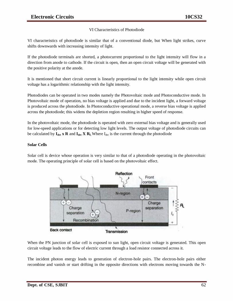
Electronic Circuits 10CS32
Dept. of CSE, SJBIT 62
VI Characteristics of Photodiode
VI characteristics of photodiode is similar that of a conventional diode, but When light strikes, curve
shifts downwards with increasing intensity of light.
If the photodiode terminals are shorted, a photocurrent proportional to the light intensity will flow in a
direction from anode to cathode. If the circuit is open, then an open circuit voltage will be generated with
the positive polarity at the anode.
It is mentioned that short circuit current is linearly proportional to the light intensity while open circuit
voltage has a logarithmic relationship with the light intensity.
Photodiodes can be operated in two modes namely the Photovoltaic mode and Photoconductive mode. In
Photovoltaic mode of operation, no bias voltage is applied and due to the incident light, a forward voltage
is produced across the photodiode. In Photoconductive operational mode, a reverse bias voltage is applied
across the photodiode; this widens the depletion region resulting in higher speed of response.
In the photovoltaic mode, the photodiode is operated with zero external bias voltage and is generally used
for low-speed applications or for detecting low light levels. The output voltage of photodiode circuits can
be calculated by Idet x R and Idet X Rf, Where Idet is the current through the photodiode
Solar Cells
Solar cell is device whose operation is very similar to that of a photodiode operating in the photovoltaic
mode. The operating principle of solar cell is based on the photovoltaic effect.
When the PN junction of solar cell is exposed to sun light, open circuit voltage is generated. This open
circuit voltage leads to the flow of electric current through a load resistor connected across it.
The incident photon energy leads to generation of electron-hole pairs. The electron-hole pairs either
recombine and vanish or start drifting in the opposite directions with electrons moving towards the N-

Electronic Circuits 10CS32
Dept. of CSE, SJBIT 63
region and holes moving towards the P-region. This accumulation of positive and negative charge carriers
constitutes the open circuit voltage.
This voltage can cause a current to flow through an external load or when the junction is shorted, the
result is a short circuit current whose magnitude is proportional to input light intensity. As the energy
produced by the individual solar cell is very less (500mV output with a load current capability of
150mA), series-parallel arrangement of solar cells is done to get the desired output. The series
combination is used to enhance the output voltage while the parallel combination is used to enhance the
current gain.
3.5 Phototransistors
The above figure shows the construction of Phototransistor. Phototransistors are usually connected in the
common-emitter configuration with the base open and the radiation is concentrated on the region near the
collector-base junction.
Symbol VI Characteristics

Electronic Circuits 10CS32
Dept. of CSE, SJBIT 64
When there is no radiation incident on the phototransistor, the collector current is due to the thermally
generated carriers, called as dark current and is given by
Ic = (β+1)Ico
Where Ico is the reverse saturation current
When light is incident on the phototransistor, photocurrent is generated and the magnitude of the collector
current increases. The expression for the collector current is given by
Ic = (β+1) (Ico+Iλ)
Where Iλ is the current generated due to incident light photons.
Phototransistor Applications
Phototransistor can be used in two configurations, namely, the common-emitter configuration and the
common-collector configuration.
In the common-emitter configuration, the output is high and goes low when light is incident on the
phototransistor, whereas in common-collector configuration, the output is high and goes to low when
light is incident on the phototransistor.
Common-Emitter mode Common-collector mode
3.6 Light-Emitting Diodes (LED)
LED is a semiconductor PN junction diode designed to emit light when forward-biased. It is one of the
most popular optoelectronic source. LEDs consume very little power and are inexpensive.

Electronic Circuits 10CS32
Dept. of CSE, SJBIT 65
PN junction of an LED
Construction of LED
When PN junction is forward biased, the electrons in the N-type material and the holes in the P-type
material travel towards the junction. Some of these holes and electrons recombine with each other and in
the process radiate energy. The energy will be released either in the form of photons of light. Gallium
Phosphide (GaP), Gallium Arsenide (GaAs) and Gallium arsenide Phosphide (GaAsP) are used in the
construction of LEDs.
In the absence of an externally applied voltage, the N-type material contains electrons while the P-type
material contains holes that can act as current carriers. When the diode is forward-biased, the energy
levels shift and there is significant increase in the concentration of electrons in the conduction band on the
N-side and that of holes in valance band on the P-side. The electrons and holes combine near the junction
to release energy in the form of photons. The process of light emission in LED is spontaneous, i.e., the
photons emitted are not in phase and travel in different directions.
The energy of the photon resulting from this recombination is equal to the bandgap energy of the
semiconductor material and is expressed by:

Electronic Circuits 10CS32
Dept. of CSE, SJBIT 66
E
1240
Where λ is the wavelength (nm) and ΔE is the bandgap energy (eV).
LED Characteristic Curve
VI Characteristics of an LED
As the LED is operated in the forward-biased mode, the VI characteristics in the forward-biased region
are shown. VI characteristics of LEDs are similar to that of conventional PN junction diodes except that
the cut-in voltage in the case of LEDs is in the range of 1.3-3V as compared to 0.7V for silicon diodes
and 0.3V for germanium diodes.
LED Parameters
1. Forward Voltage (VF): It is the DC voltage across the LED when it is ON. 2. Candle Power (CP): It is a measure of the luminous intensity or the brightness of the light emitted by
the LED. It is a non-linear function of LED current and the value of CP increases with increase in the
current flowing through the LED. 3. Radiant Power Output (Po): It is the light power of the LED.
4. Peak Spectral Emission (λP): It is the wavelength where the intensity of light emitted by the LED is
maximum.
5. Spectral Bandwidth: It is the measure of concentration of color brightness around the LEDs nominal
wavelength.
LED Drive Circuit

Electronic Circuits 10CS32
Dept. of CSE, SJBIT 67
Connecting LEDs in Parallel Connecting LEDs in Series
LEDs are operated in the forward-biased mode. As the current through the LED changes very rapidly
with change in forward voltage above the threshold voltage, LEDs are current-driven devices. The resistor
(R) is used limit the current flowing through the device. A silicon diode can be placed inversely parallel
to the LED for reverse polarity voltage protection.
The current that will flow through the LED is given by
R
VVI FCC
The value of the resistor (R) to be connected is given by
I
VVVVVR FnFFFCC
........321
Liquid Crystal Displays (LCD)
Liquid Crystals are materials that exhibit properties of both solids and liquids, that is, they are an
intermediate phase of matter. They can be classified into three different groups: nematic, smectic and
cholestric. Nematic liquid crystals are generally used in the fabrication of liquid crystal displays (LCDs)
with the twisted nematic material being the most common.
Construction of an LCD
Construction of LCD Display Operation of LCD Display
Electronic Circuits 10CS32
Dept. of CSE, SJBIT 68
An LCD display consists of liquid-crystal fluid, conductive electrodes, a set of polarizers and a glass
casing. The outermost layers are the polarizers which are housed on the outer surface of the glass casing.
The polarizer attached to the front glass is referred to as the front polarizer, while the one attached to the
attached to the rear glass is the rear polarizer.
On the inner surface of the glass casing, transparent electrodes are placed in the shape of desired image.
The electrode attached to the front glass is referred to as the segment electrode while the one attached to
the rear glass is the backplane or the common electrode. The liquid crystal is sandwiched between the two
electrodes.
Operation
The basic principle of operation of LCD is to control the transmission of light by changing the
polarization of the light passing through the liquid crystal with the help of an externally applied voltage.
As LCDs do not emit their own light, backlighting is used to enhance the legibility of the display in dark
conditions.
LCDs have the capability to produce both positive as well as negative images. A positive image is defined
as a dark image on a light background. In a positive image display, the front and rear polarizers are
perpendicular to each other. Light entering the display is guided by the orientation of the liquid crystal
molecules that are twisted by 90o from the front glass plate to the rear glass plate. This twist allows the
incoming light to pass through the second polarizer. When a light is applied to the display, the liquid
crystal molecules straighten out and stop redirecting the light. As a result light travels straight through and
is filtered out by the second polarizer. Therefore, no light can pass through, making this region darker
compared to the rest of the screen. Hence, in order to display characters or graphics, voltage is applied to
the desired regions, making them dark and visible to the eye.
A negative image is a light image on a dark background. In negative image displays, the front and the rear
polarizers are aligned parallel to each other.
Driving an LCD
LCD can be classified as direct-drive and multiplex-drive displays depending upon the technique used to
drive them. Direct-drive displays, also known as static-drive displays, have an independent driver for each
pixel. The voltage in this case is a square waveform having two voltage levels, namely, ground and Vcc.
As the display size increases the drive circuitry becomes very complex. Hence, multiplex drive circuits
are used for larger size displays. These displays reduce the total number of interconnections between the
LCD and the driver. They have more than one backplane and the driver produces an amplitude-varying,
time-synchronized waveform for both segment and backplanes.
LCD Response Time
The LCD response time is defined by the ON and OFF response times.

Electronic Circuits 10CS32
Dept. of CSE, SJBIT 69
ON time refers to the time required by an OFF pixel to become visible after the application of proper
drive voltage. The OFF time is defined as the time required by the ON pixel to turn OFF after the
application of proper drive voltage.
The response time of LCDs varies widely with temperature and increase rapidly at low operating
temperatures.
Liquid Crystal Display Types
LCDs are non-emissive devices, that is, they do not generate light on their own. Depending upon the
mode of transmission of light in an LCD, they are classified:
Reflective LCD displays:
Reflective LCD displays have a reflector attached to the rear polarizer which reflects incoming light
evenly back into the display. These displays rely on the ambient light to operate and do not work in the
dark conditions. They produce only positive images. The front and the rear polarizers are perpendicular to
each other. These types of displays are commonly used in calculators and digital wrist watches.
Transmissive LCD displays:
In transmissive LCD displays, back light is used as the light source. Most of these displays operate in the
negative mode, that is, the text will be displayed in light color and the background is dark color.
Transmissive displays are good for very low light level conditions. They offer very poor contrast when
used in direct sunlight and provide good picture quality indoors. They are generally used in medical
devices, electronic test and measuring equipments and in laptops.
Transreflective LCD displays

Electronic Circuits 10CS32
Dept. of CSE, SJBIT 70
Transreflective displays are a combination of reflective and transmissive displays. A white or silver
translucent material is applied to the rear of the display, which reflects some of the ambient light back to
the observer. It also allows the backlight to pass through. They are good for displays operating in varying
light conditions.
Active and Passive LCD displays
LCD displays are classified as passive LCD displays and active LCD displays depending upon the nature
of the activation circuit.
Passive displays use components that do not supply their own energy to turn ON or OFF the desired pixel.
Active displays use an active device such as a transistor or diode in each which acts like a switch that
precisely controls the voltage that each pixel receives.
Advantages and Disadvantages
LCD displays are not active sources of light
They offer very low power consumption, low operating voltages and good flexibility
Their response time is too slow for many applications
They offer limited viewing angle and are temperature sensitive
3.7 Cathode Ray Tube Displays
Cathode Ray Tube (CRT) displays are used in a wide range of systems ranging from consumer electronic
systems like television and computer monitors to measuring instruments like oscilloscopes to military
systems like radar and so on. CRT display is a specialized vacuum tube in which the images are produced
when the electron beam strikes the fluorescent screen. CRT displays can be monochrome displays as well
as colored displays.

Electronic Circuits 10CS32
Dept. of CSE, SJBIT 71
Monochrome CRT displays comprise a single electron gun, a fluorescent screen and an internal or
external mechanism to accelerate and deflect the electron beam. The electron gun produces a narrow
beam of electrons that are accelerated by the anodes. There are two sets of deflecting coils, namely, the
horizontal coil and the vertical coil. These coils produce an extremely low frequency electromagnetic
field in the horizontal and vertical directions to adjust the direction of the electron beam. CRT tubes also
have a mechanism to vary the intensity of the electron beam. In order to produce moving pictures in
natural colors on the screen, complex signals are applied to the deflecting coils and to the circuitry
responsible for controlling the intensity of the electron beam. This results in movement of the spot from
right to left and from top to bottom of the screen. The speed of the spot movement is so fast that the
person viewing the screen sees a constant image on the entire screen.
Color CRT displays comprises three electron guns, one each for the three primary colors namely red, blue
and green. The CRT produces three overlapping images, one in red, one in green and one in blue. This is
referred to as the RGB color model.
Advantages and Disadvantages
CRT displays offer very high resolution and these displays emit their own light; therefore, they have
very high value of peak luminance.
They offer wide viewing angles of the order of 180o.
CRT displays are bulky and consume significant power.
They require high voltages to operate and they cause fatigue and strain to the human eye.
3.8 Emerging Display Technologies
Organic Light-Emitting Diodes (OLEDs)
OLEDs are composed of a light-emitting organic material sandwiched between two conducting plates,
one of N-type material and the other of P-type material. When an electric potential is applied between
these plates, holes are ejected from the P-type plate and electrons are ejected from the N-type plate.
Recombination of these holes and electrons, energy is released in the form of light photons. The
wavelength of light emitted depends upon the bandgap energy of the semiconductor material used.
OLEDs can be classified into three types, namely, small molecule OLEDs (SMOLED), polymer LEDs
(PLED) and dendrimer OLEDs.
Digital Light Processing Technology (DLP)
DLP technology makes use of an optical semiconductor device referred to as digital micromirror device
(DMD) which is basically a precise light switch that can digitally modulate light through a large number
of microscopic mirrors arranged in a rectangular array. These mirrors are mounted on tiny hinges and can
be tilted away or towards the light source with the help of DMD chip and thus projecting a light or a dark
pixel on the screen. Use of DLP technology is currently limited to large projection systems.

Electronic Circuits 10CS32
Dept. of CSE, SJBIT 72
Plasma Display Panels (PDP)
Plasma displays are composed of millions of cells sandwiched between two panels of glass. Two
electrodes, namely, the address electrodes and display electrodes, are also placed between the two glass
plates covering the entire screen. The address electrodes are printed on the rear glass plate and the
transparent display electrodes are located above the cells along the front glass plate. These electrodes are
perpendicular to each other forming a grid network. Each cell is filled with xenon and neon gas mixture.
The electrodes intersecting at a specific cell are charged to excite the gas mixture in that cell. When the
gas mixture is excited, plasma is created releasing ultraviolet light which then excites the phosphor
electrons located on the sides of the cells. These electrons in turn release visible light and return to their
lower energy state. Each pixel is composed of three cells containing red, green and blue phosphors.
Plasma displays offer advantages like each pixel generates its own light offering large viewing angles,
generates super image quality and the image quality is not affected by the area of the display, but these
displays are fragile in nature and are susceptible to burn-out from static images
Field Emission Displays
FEDs function like CRT displays with the main difference being that these displays use millions of small
electron guns to emit electrons at the screen instead of just one as in case of CRT. FED displays produce
the same quality of image as produced by the CRT displays without being bulky as the CRT displays.
These displays can be as thin as LCD and as large as Plasma.
Electronic Ink Displays
Electronic ink displays, also referred to as electronic paper, are active matrix displays making use of
pigments that resemble the ink used in print.
3.9 Optocouplers
An optocoupler, also referred to as an optoisolator, is a device that uses a short optical transmission path
to transfer signals between the elements of a circuit. Optocouplers are sealed units that house an optical
transmitting device and a photosensitive device that are coupled together optically. The optical path may
be air or a dielectric waveguide.
Optical Path
Optical
transmitting
device
Photo-
Sensitive
device
Vin Vo

Electronic Circuits 10CS32
Dept. of CSE, SJBIT 73
Optocoupler Parameters
The important parameters that define the performance of an optocoupler are
1. Forward Optocoupling Efficiency: It is specified in terms of current transfer ratio (CTR). CTR is the
ratio of the output current to the input current. 2. Isolation Voltage: It is the maximum permissible DC potential that can be allowed to exist between
the input and the output circuits.
3. Input Current: It is the maximum permissible forward current that is allowed to flow into the transmitting LED.
4. VCE(max): It is the transistor‟s maximum collector-emitter voltage rating. It limits the supply voltage
that can be applied to the output circuit.
5. Bandwidth: It determines the maximum signal frequency that can be successfully passed through the
optocouplers. The bandwidth of an optocoupler depends upon its switching speed.
Optocoupler Configurations
Non-Latching Optocoupler Configuration:
Photodiode Phototransistor Photo-Darlington Transistors
Photoconductor PhotoFET
Latching Optocoupler Configuration:
PhotoSCR PhotoDIAC PhotoTRIAC

Electronic Circuits 10CS32
Dept. of CSE, SJBIT 74
Advantages
Complete electrical isolation between input and output circuit
Less response time of optocouplers enable data transmission in MHz range
Capable of wideband signal transmission
Unidirectional signal transfer, output does not loop back to the input circuit
Easy interface with logic devices
Compact and light weight
Noise, transients, contact bounce etc. are completely eliminated
3.10 Recommended Questions
1. Derive the equation for Av, Ai , Zi, and Zo for a common emitter amplifier
2. Derive the expression for voltage gain for two stage CE amplifier.
3. Draw and explain the working of swamped amplifier.
4. What are the advantages of swamped amplifier?
5. Draw and explain the working of two-stage feedback amplifier.
6. Derive the equation for Av, Ai, Zi, and Zo for the CC amplifier.
7. Derive the equation for Av, Ai, Zi, and Zo for CB amplifier.
8. Draw and explain the two transistor regulator.
9. Draw and explain the Zener follower voltage regulator.
10. Draw and explain the cascaded CE and CC stages of an amplifier.
11. Derive the expression for voltage gain of the CE-CC cascaded amplifier.
12. Explain how h-parameter can be obtained from the transistor characteristics.
13. The transistor amplifier shown in the figure below uses a transistor whose h-parameters are hie =
1.1kΩ, hfe = 50, hre = 2.5x10⁻⁴
and 1/hoe = 40kΩ. Calculate Ai = Io/Ii, Av, Avs, Ro and Ri (Aug-2005)
14. Draw the „h‟ parameter equivalent circuit for a typical common emitter amplifier and Derive the
expression for Ai , Ri , and Av
15. For the amplifier shown in the figure below calculate Ri, R‟i, Av, Avs and Ai= -(I2/I1). The transistor parameters are hie=1.1kΩ, hre = 2.5x10
-4, hfe = 50 and hoe = 25µA/V. (Aug-2004, 2005)
16. Explain how h-parameters can be obtained from the static characteristics of a transistor. (Jan-
2007)

Electronic Circuits 10CS32
Dept. of CSE, SJBIT 75
UNIT – 4: Small Signal Analysis of Amplifiers
4.1 Basic FET Amplifiers
In the last chapter, we described the operation of the FET, in particular the MOSFET, and analyzed and
designed the dc response of circuits containing these devices. In this chapter, we emphasize the use of
FETs in linear amplifier applications. Although a major use of MOSFETs is in digital applications, they
are also used in linear amplifier circuits.
There are three basic configurations of single-stage or single-transistor FET amplifiers. These are the
common-source, source-follower, and common-gate configurations. We investigate the characteristics of
each configuration and show how these properties are used in various applications. Since MOSFET
integrated circuit amplifiers normally use MOSFETs as load devices instead of resistors because of their
small size, we introduce the technique of using MOSFET enhancement or depletion devices as loads.
These three configurations form the building blocks for more complex amplifiers, so gaining a good
understanding of these three amplifier circuits is an important goal of this chapter.
In integrated circuit systems, amplifiers are usually connected in series or cascade, forming a multistage
configuration, to increase the overall voltage gain, or to provide a particular combination of voltage gain
and output resistance. We consider a few of the many possible multistage configurations, to introduce the
analysis methods required for such circuits, as well as their properties.
4.2 THE MOSFET AMPLIFIER
We discussed the reasons linear amplifiers are necessary in analog electronic systems. In this chapter, we
continue the analysis and design of linear amplifiers that use field-effect transistors as the amplifying
device. The term small signal means that we can linearize the ac equivalent circuit. We will define what
is meant by small signal in the case of MOSFET circuits. The term linear amplifiers means that we can
use superposition so that the dc analysis and ac analysis of the circuits can be performed separately and
the total response is the sum of the two individual responses.
The mechanism with which MOSFET circuits amplify small time-varying signals was introduced in the
last chapter. In this section, we will expand that discussion using the graphical technique, dc load line,
and ac load line. In the process, we will develop the various small-signal parameters of linear circuits and
the corresponding equivalent circuits.
There are four possible equivalent circuits that can he used.

Electronic Circuits 10CS32
Dept. of CSE, SJBIT 76
The most common equivalent circuit that is used for the FET amplifiers is the transconductance amplifier,
in which the input signal is a voltage and the output signal is a current.
Graphical Analysis, Load Lines, and Small-Signal Parameters
Figure 6. 1 shows an NMOS common-source circuit with a time-varying voltage source in series with the
dc source. We assume the time-varying input signal is sinusoidal. Figure 6.2 shows the transistor
characteristics, dc load line, and Q-point, where the dc load line and Q-point are functions of vGS, VDD, RD
and the transistor parameters.

Electronic Circuits 10CS32
Dept. of CSE, SJBIT 77
For the output voltage to be a linear function of the input voltage, the transistor must be biased in the
saturation region. Note that, although we primarily use n-channel, enhancement -mode MOSFETs in our
discussions, the same results apply to the other MOSFETs.
Also shown in Figure 6.2 are the sinusoidal variations in the gate-to-source voltage, drain current, and
drain-to-source voltage, as a result of the sinusoidal source vi. The total gate-to-source voltage is the sum
of VGSQ and vi. As vi increases, the instantaneous value of vGS increases, and the bias point moves up the
load line. A larger value of vGS means a larger drain current and a smaller value of vDS. Once the Q-point
is established, we can develop a mathematical model for the sinusoidal, or small-signal, variations in the
gate-to-source voltage, drain-to-source voltage, and drain current.
The time-varying signal source in Figure 6.1 generates a time-varying component of the gate-to-source
voltage. For the FET to operate as a linear amplifier, the transistor must be biased in the saturation
region, and the instantaneous drain current and drain-to-source voltage must also be confined to the
saturation region.

Electronic Circuits 10CS32
Dept. of CSE, SJBIT 78
Transistor Parameters

Electronic Circuits 10CS32
Dept. of CSE, SJBIT 79

Electronic Circuits 10CS32
Dept. of CSE, SJBIT 80

Electronic Circuits 10CS32
Dept. of CSE, SJBIT 81
source is assumed to be constant, the sinusoidal current produces no sinusoidal voltage component across
this element. The equivalent ac impedance is therefore zero, or a short circuit. Consequently, in the ac
equivalent circuit, the dc voltage sources are equal to zero. We say that the node connecting RD and VDD
is at signal ground.
4.3 Small-Signal Equivalent Circuit
Now that we have the ac equivalent circuit for the NMOS amplifier circuit, (Figure 6.4), we must develop
a small-signal equivalent circuit for the transistor.
Initially, we assume that the signal frequency is sufficiently low so that any capacitance at the gate
terminal can be neglected. The input to the gate thus appears as an open circuit, or an infinite resistance.
Eq. 6.14 relates the small-signal drain current to the small-signal input voltage and Eq. 6.7 shows that the
transconductance is a function of the Q-point. The resulting simplified small-signal equivalent circuit for
the NMOS device is shown in Figure 6.5. (The phasor components are in parentheses.)

Electronic Circuits 10CS32
Dept. of CSE, SJBIT 82
This small-signal equivalent circuit can also he expanded to take into account the finite output resistance
of a MOSFET biased in the saturation region. This effect, discussed in the previous chapter, is a result of
the nonzero slope in the iD versus vDS curve. We know that
The expanded small-signal equivalent circuit of the n-channel MOSFET is shown in Figure 6.6 in phasor
notation.
We note that the small-signal equivalent circuit for the MOSFET circuit is very similar to that of the BJT
circuits.

Electronic Circuits 10CS32
Dept. of CSE, SJBIT 83
Comment: Because of the relatively low value of transconductance, MOSFET circuits tend to have a
lower small-signal voltage gain than comparable bipolar circuits. Also, the small-signal voltage gain
contains a minus sign, which means that the sinusoidal output voltage is 180 degrees out of phase with
respect to the input sinusoidal signal
4.4 Problem-Solving Technique: MOSFET AC Analysis
Since we are dealing with linear amplifiers, superposition applies, which means that we can perform the
dc and ac analyses separately. The analysis of the MOSFET amplifier proceeds as follows:
1. Analyze the circuit with only the dc sources present. This solution is the dc or quiescent solution. The
transistor must he biased in the saturation region in order to produce a linear amplifier.

Electronic Circuits 10CS32
Dept. of CSE, SJBIT 84
2. Replace each element in the circuit with its small-signal model, which means replacing the transistor by
its small-signal equivalent circuit.
3. Analyze the small-signal equivalent circuit, setting the dc source components equal to zero, to produce
the response of the circuit to the time-varying input signals only.
The previous discussion was for an n-channel MOSFET amplifier. The same basic analysts and
equivalent circuit also applies to the p-channel transistor. Figure 6.8(a) shows a circuit containing a p-
channel MOSFET.
Note that the power supply voltage is connected to the source. (The subscript DD can be used to indicate
that the supply is connected to the drain terminal Here, however, VDD, is simply the usual notation for the
power supply voltage in MOSFET circuits.) Also note the change in current directions and voltage
polarities compared to the circuit containing the NMOS transistor. Figure 6.8(b) shows the ac equivalent
circuit, with the dc voltage sources replaced
The final small-signal equivalent circuit of the p-channel MOSFET amplifier is shown in Figure 6.10

Electronic Circuits 10CS32
Dept. of CSE, SJBIT 85
We also note that the expression for the small-signal voltage gain of the p-channel MOSFET amplifier is
exactly the same as that for the n-channel MOSFET amplifier. The negative sign indicates that a 180-
degree phase reversal exists between the output and input signals, for both the PMOS and the NMOS
circuit.
4.5 Basic Transistor Amplifier Configurations
As we have seen, the MOSFET is a three-terminal device (actually 4 counting the substrate). Three basic
single-transistor amplifier configurations can be formed, depending on which of the three transistor
terminals is used as signal ground. These three basic configurations are appropriately called common
source, common drain (source follower), and common gate. These three circuit configurations correspond
to the common-emitter, emitter-follower, and common-base configurations using BJTs.
The input and output resistance characteristics of amplifiers are important in determining loading effects.
These parameters, as well as voltage gain, for the three basic MOSFET circuit configurations will be
determined in the following sections.
THE COMMON-SOURCE AMPLIFIER
In this section, we consider the first of the three basic circuits; the common-source amplifier. We will
analyze several basic common-source circuits, and will determine small-signal voltage gain and input and
output impedances.
A Basic Common-Source Configuration
For the circuit shown in Figure 6.13, assume that the transistor is biased in the saturation region by
resistors R1 and R2, and that the signal frequency is sufficiently large for the coupling capacitor to act
essentially as a short circuit. The signal source is represented by a Thevenin equivalent circuit, in which
the signal voltage source vi, is in series with an equivalent source resistance RSi. As we will see, RSi
should be much less than the amplifier input resistance, Ri = R1 || R2 in order to minimize loading effects.

Electronic Circuits 10CS32
Dept. of CSE, SJBIT 86
Figure 6.14 shows the resulting small-signal equivalent circuit. The small signal variables, such as the
input signal voltage Vi are given in phasor form.
The output voltage is

Electronic Circuits 10CS32
Dept. of CSE, SJBIT 87
The input and output resistances of the amplifier can be determined from Figure 6.14. The input
resistance to the amplifier is Ris = R1 || R2. Since the low-frequency input resistance looking into the gate
of the MOSFET is essentially infinite, the input resistance is only a function of the bias resistors. The
output resistance looking hack into the output terminals is found by setting the independent input source
Vi equal to zero, which means that VGS = 0. The output resistance is therefore Ro = RD || ro.

Electronic Circuits 10CS32
Dept. of CSE, SJBIT 88
Common-Source Amplifier with Source Resistor
A source resistor RS tends to stabilize the Q-point against variations in transistor parameters (Figure 6.18).
If, for example, the value of the conduction parameter varies from one transistor to another, the Q-point
will not vary as much if a source resistor is included in the circuit. However, as shown in the following
example, a source resistor also reduces the signal gain. This same effect was observed in BJT circuits
when an emitter resistor was included.
The circuit in Figure 6.18 is an example of a situation in which the body effect (not discussed) should be
taken into account. The substrate (not shown) would normally be connected to the -5 V supply, so that the
body and substrate terminals are not at the same potential. However, in the following example, we will
neglect this effect.

Electronic Circuits 10CS32
Dept. of CSE, SJBIT 89

Electronic Circuits 10CS32
Dept. of CSE, SJBIT 90
Common-Source Circuit with Source Bypass Capacitor
A source bypass capacitor added to the common-source circuit with a source resistor will minimize the
loss in the small-signal voltage gain, while maintaining Q-point stability. The Q-point stability can be
further increased by replacing the source resistor with a constant-current source. The resulting circuit is
shown in Figure 6.22, assuming an ideal signal source. If the signal frequency is sufficiently large so that
the bypass capacitor acts essentially as an ac short-circuit, the source will be held at signal ground.

Electronic Circuits 10CS32
Dept. of CSE, SJBIT 91

Electronic Circuits 10CS32
Dept. of CSE, SJBIT 92
4.6 The Source-Follower Amplifer
The second type of MOSFE'T amplifier to be considered is the common-drain circuit. An example of this
circuit configuration is shown in Figure 6.28.
As seen in this figure, the output signal is taken off the source with respect to ground and the drain is
connected directly to VDD. Since VDD becomes signal ground in the ac equivalent circuit, we get the name
common drain, but the more common name is a source follower. The reason for this name will become
apparent as we proceed through the analysis.
Small-Signal Voltage Gain

Electronic Circuits 10CS32
Dept. of CSE, SJBIT 93

Electronic Circuits 10CS32
Dept. of CSE, SJBIT 94

Electronic Circuits 10CS32
Dept. of CSE, SJBIT 95
4.7 Input and Output impedance
The input resistance Ri, as defined in Figure 6.29b), is the Thevenin equivalent resistance of the bias
resistors. Even though the input resistance to the gate of the MOSFET is essentially infinite, the input
bias resistances do create a loading effect. This same effect was seen in the common-source circuits.
To calculate the output resistance, we set all independent small-signal sources equal to zero, apply a test
voltage to the output terminals, and measure a test current. Figure 6.31 shows the circuit we will use to
determine the output resistance of the source follower shown in Figure 6.28.
We set Vi = 0 and apply a test voltage Vx. Since there are no capacitances in the circuit, the output
impedance is simply an output resistance, which is defined as
Ro = Vx / Ix

Electronic Circuits 10CS32
Dept. of CSE, SJBIT 96
4.8 The Common-Gate Configuration
The third amplifier configuration is the common-gate circuit. To determine the small-signal voltage and
current gains, and the input and output impedances, we will use the same small-signal equivalent circuit
for the transistor that was used previously. The dc analysis of the common-gate circuit is the same as that
of previous MOSFET circuits.
Small-Signal Voltage and Current Gains
In the common-gate configuration, the input signal is applied to the source terminal and the gate is at
signal ground. The common-gate configuration shown in Figure 6.344 is biased with a constant-current
source IQ.

Electronic Circuits 10CS32
Dept. of CSE, SJBIT 97
The gate resistor RG prevents the buildup of static charge on the gate terminal, and the capacitor CG
ensures that the gate is at signal ground. The coupling capacitor CC1 couples the signal to the source, and
coupling capacitor CC2 couples the output voltage to load resistance RL.
The small-signal equivalent circuit is shown in Figure 6.35. The small-signal transistor resistance rO is
assumed to be infinite.
The output voltage is

Electronic Circuits 10CS32
Dept. of CSE, SJBIT 98
Input and Output Impedance
In contrast to the common-source and source-follower amplifiers, the common-gate circuit has a low
input resistance because of the transistor. However, if the input signal is a current, a low input resistance
is an advantage. The input resistance is defined as

Electronic Circuits 10CS32
Dept. of CSE, SJBIT 99
4.9 The Three Basic Amplifier Configurations: Summary and Comparison
Table 6.1 is a summary of die small-signal characteristics of the three amplifier configurations.
The input resistance looking directly into the gate of the common-source and source-follower circuits is
essentially infinite at low to moderate signal frequencies. However, the input resistance, of these discrete
amplifiers is the Thevenin equivalent resistance RTH of the bias resistors. In contrast, the input resistance
to the common-gate circuit is generally in the range of a few hundred ohms.
The output resistance of the source follower is generally in the range of a few hundred ohms. The output
resistance of the common-source and common-gate configurations is dominated by the resistance RD.
The specific characteristics of these single-stage amplifiers are used in the design of multistage
amplifiers.
In the last chapter, we considered three all-MOSFET inverters and plotted the voltage transfer
characteristics. All three inverters use an n-channel enhancement-mode driver transistor. The three types
of load devices are an n-channel enhancement-mode device, an n-channel depletion-mode device, and a
p-channel enhancement-mode device. The MOS transistor used as a load device is referred to as an active
load. We mentioned that these three circuits can be used as amplifiers.
In this section, we revisit these three circuits and consider their amplifier characteristics. We will
emphasize the small-signal equivalent circuits. This section serves as an introduction to more advanced
MOS integrated circuit amplifier designs considered in Part II of the text.
NMOS Amplifiers with Enhancement Load
The characteristics of an n-channel enhancement toad device were presented in the last chapter. Figure
6.38(a) shows an NMOS enhancement load transistor.

Electronic Circuits 10CS32
Dept. of CSE, SJBIT 100
and Figure 6.38b) shows the current-voltage characteristics. The threshold voltage is VTNL.
Figure 6.39(a) shows an NMOS amplifier with an enhancement load.

Electronic Circuits 10CS32
Dept. of CSE, SJBIT 101
The driver transistor is MD and the load transistor is ML. The characteristics of transistor MD and the load
curve are shown in Figure 6.39(b). The load curve is essentially the mirror image of the i-v characteristic
of the load device. Since the i-v characteristics of the load device are nonlinear, the load curve is also
nonlinear. The load curve intersects the voltage axis at VDD – VTNL, which is the point where the current
in the enhancement load device goes to zero. The transition point is also shown on the curve.
The voltage transfer characteristic is also useful in visualizing the operation of the amplifier. This curve is
shown in Figure 6.39(c). When the enhancement-mode driver first begins to conduct, it is biased in the
saturation region. For use as an amplifier, the circuit Q-point should be in this region, as shown in both
Figures 6.39b) and (c).
We can now apply the small-signal equivalent circuits to find the voltage gain. In the discussion of the
source follower, we found that the equivalent resistance looking into the source terminal (with RS = ∞)
was
RO = (l / gm) || rO. The small-signal equivalent circuit of the inverter is given in Figure 6.40, where the
subscripts D and L refer to the driver and load transistors, respectively. We are again neglecting the body
effect of the load transistor.
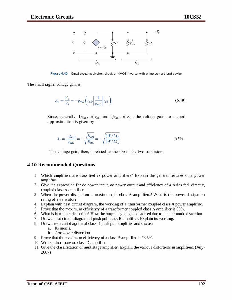
Electronic Circuits 10CS32
Dept. of CSE, SJBIT 102
The small-signal voltage gain is
4.10 Recommended Questions
1. Which amplifiers are classified as power amplifiers? Explain the general features of a power amplifier.
2. Give the expression for dc power input, ac power output and efficiency of a series fed, directly,
coupled class A amplifier.
3. When the power dissipation is maximum, in class A amplifiers? What is the power dissipation rating of a transistor?
4. Explain with neat circuit diagram, the working of a transformer coupled class A power amplifier.
5. Prove that the maximum efficiency of a transformer coupled class A amplifier is 50%. 6. What is harmonic distortion? How the output signal gets distorted due to the harmonic distortion.
7. Draw a neat circuit diagram of push pull class B amplifier. Explain its working.
8. Draw the circuit diagram of class B push pull amplifier and discuss
a. Its merits. b. Cross-over distortion
9. Prove that the maximum efficiency of a class B amplifier is 78.5%.
10. Write a short note on class D amplifier. 11. Give the classification of multistage amplifier. Explain the various distortions in amplifiers. (July-
2007)

Electronic Circuits 10CS32
Dept. of CSE, SJBIT 103
Unit – 5: Large Signal Amplifiers
Large signal or power amplifiers provide power amplification and are used in applications to provide
sufficient power to the load or the power device. The output power delivered by these amplifiers is of the
order of few watts to few tens of watts. They handle moderate-to-high levels of current and voltage
signals as against small levels of current and voltage signals in the case of small signal amplifiers.
5.1 Classification of Large Signal Amplifiers
On the basis of their circuit configurations and principle of operation, amplifiers are classified into
different classes.
Class A Amplifiers
A class A power amplifier is defined as a power amplifier in which output current flows for the full-cycle
(360°) of the input signal. In other words, the transistor remains forward biased throughout the input
cycle. The active device in a class A amplifier operates during the whole during the whole of the input
cycle and the output signal is an amplified replica of the input signal with no clipping. The amplifying
element is so biased that it operates over the linear region of its output characteristics during full period of
the input cycle and is always conducting to some extent.
Class A amplifiers offer very poor efficiency and a maximum of 50% efficiency is possible in these
amplifiers
Class B Amplifier
Class B amplifiers operate only during the half of the input cycle. Class B amplifiers offer much
improved efficiency over class A amplifiers with a possible maximum of 78.5%. They also create a large
amount of distortion.

Electronic Circuits 10CS32
Dept. of CSE, SJBIT 104
Class AB Amplifier
In a class AB amplifier, the amplifying device conducts for a little more than half of the input waveform.
They sacrifice some efficiency over class B amplifiers but they offer better linearity than class B
amplifier. They offer much more efficiency than class A amplifiers.
Class C Amplifiers
Class C amplifiers conducts for less than half cycle of the input signal resulting in a very high efficiencies
up to 90%. But they are associated with very high level of distortion at the output. Class C amplifiers
operate in two modes, namely, the tuned mode and the unturned mode.
Class D Amplifiers
Class D amplifiers use the active device in switching mode to regulate the output power. These amplifiers
offer high efficiencies and do not require heat sinks and transformers. These amplifiers use pulse width
modulation (PWM), pulse density modulation or sigma delta modulation to convert the input signal into a
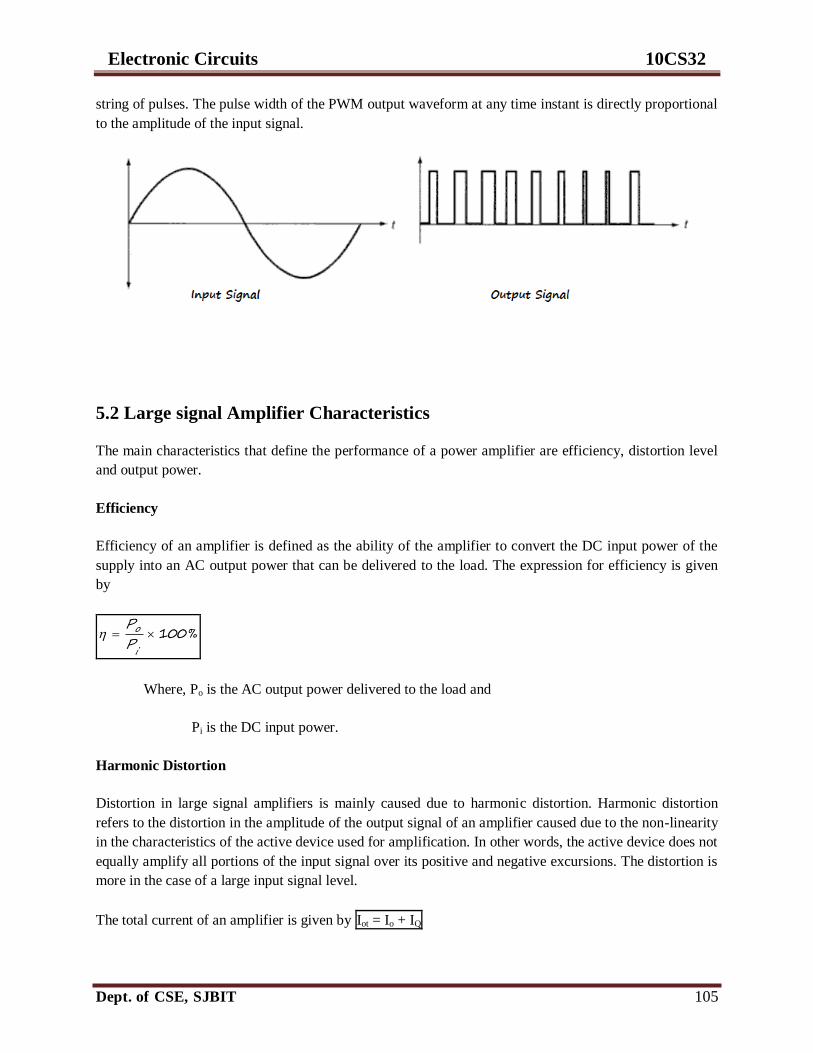
Electronic Circuits 10CS32
Dept. of CSE, SJBIT 105
string of pulses. The pulse width of the PWM output waveform at any time instant is directly proportional
to the amplitude of the input signal.
5.2 Large signal Amplifier Characteristics
The main characteristics that define the performance of a power amplifier are efficiency, distortion level
and output power.
Efficiency
Efficiency of an amplifier is defined as the ability of the amplifier to convert the DC input power of the
supply into an AC output power that can be delivered to the load. The expression for efficiency is given
by
%100
i
o
PP
Where, Po is the AC output power delivered to the load and
Pi is the DC input power.
Harmonic Distortion
Distortion in large signal amplifiers is mainly caused due to harmonic distortion. Harmonic distortion
refers to the distortion in the amplitude of the output signal of an amplifier caused due to the non-linearity
in the characteristics of the active device used for amplification. In other words, the active device does not
equally amplify all portions of the input signal over its positive and negative excursions. The distortion is
more in the case of a large input signal level.
The total current of an amplifier is given by Iot = Io + IQ

Electronic Circuits 10CS32
Dept. of CSE, SJBIT 106
Where Io is the alternating portion of the output current and
IQ is the output DC current under quiescent condition.
Where Io = A0 + A1cosωt + A2cos2ωt
Iot = IQ + A0 + A1cosωt + A2cos2ωt
Where A0 is the extra DC component due to rectification of the signal;
A1 is the amplitude of the desired signal at the fundamental input signal frequency ω;
A2 is the amplitude of the desired signal at the fundamental input signal frequency 2ω;
Second harmonic distortion is a measure of the relative amount of second harmonic component to
the fundamental frequency component and is expressed as %1001
22
A
AD
IIIly the third harmonic distortion component (D3) is given by %100
1
33
AA
D
The fourth harmonic distortion component (D3) is given by %1001
44
A
AD
The total harmonic distortion (D) is given by the square root of the mean square of the individual
harmonic components.
...24
23
22 DDDD
The power delivered at the fundamental frequency is 2
21
1LRA
P
The total power output is given by 2
...)( 23
22
21
LRAAAP
Therefore, 123
22 ...)1( PDDP
12 )1( PDP

Electronic Circuits 10CS32
Dept. of CSE, SJBIT 107
5.3 Feedback Amplifiers
Classification of Amplifiers
On the basis of the input and output parameters of interest, amplifiers are classified as voltage amplifiers,
current amplifiers, transresistance and transconductance amplifiers.
In the case of a voltage amplifier, a small change in the input voltage produces a large change in the
output voltage. Voltage gain, which is the ratio of the change in the output voltage to change in the input
voltage, is the gain parameter.
In the case of a current amplifier, a small change in the input current produces a large change in the
output current. Current gain, which is the ratio of change in the output current to the change in the input
current, is the gain parameter.
In the case of a transresistance amplifier, a small change in the input current produces a large change in
the output voltage. Ratio of the change in the output voltage to change in the input current is the gain
parameter. The gain parameter has the units of resistance.
In the case of a transconductance amplifier, a small change in the input voltage produces a large change in
the output current. Ratio of the change in the output current to the change in the input voltage is the gain
parameter. The gain parameter has the units of conductance.
Amplifier with Negative Feedback
In a negative feedback amplifier, a sample of the output signal is fed back to the input and the feedback
signal is combined with the externally applied input signal in a subtractor circuit as shown in the figure
below.
The actual signal Xi applied to the basic amplifier is the difference of the externally applied input signal
Xs and the feedback signal Xf. The generalized representation of input and output signals is intended to
indicate that the signal could either be a current or a voltage signal.
Basic amplifier
(A)
Feedback network
(β)
Σ XS +
-
_
Xi
Xf = βXo
Xo

Electronic Circuits 10CS32
Dept. of CSE, SJBIT 108
The gain parameters could be a voltage gain, current gain, transresistance or transconductance. The gain
has two values namely gain of the basic amplifier without feedback and the gain of the amplifier with
feedback.
From the above circuit, the actual signal applied to the amplifier input Xi is the difference of externally
applied input signal Xs and the feedback signal Xf. It is given by
Xi = Xs – Xf --- (1)
Also, Xf = βXo, Xo = AXi and Xo = AfXs
Substituting for Xi and Xf in eq (1) we get
oso βXX
A
X
Simplifying the equation we get
βA1A
X
XA
s
of
The feedback is expressed in decibels. It is given by
βA11
20log A
A20log feedback of dB f
The three important assumptions to be satisfied by a feedback network is,
1. The input signal is transmitted to the output through the amplifier only and not through the
feedback network. That is, forward transmission through feedback network is zero. This further implies that if the gain of the amplifier were reduced to zero, the output must drop to zero.
2. The feedback signal is transmitted from output to input through feedback network only. That is,
reverse transmission through amplifier is zero.
3. The feedback factor is independent of load and source resistance.
Signal
Source
Subtractor Basic
Amplifier (A)
Sampling
Network
Feedback
Network (β)
Is
Vs +
- RL
+
- Vo +
-
Vf +
-
If
Ii Io Ii

Electronic Circuits 10CS32
Dept. of CSE, SJBIT 109
Advantages of Negative Feedback
1. Gain parameter is independent of variation in values of components used in building the basic
amplifier. 2. Bandwidth is increased.
3. Distortion is reduced and linearity is increased.
4. Noise is reduced. 5. Input resistance can be reduced or decreased depending on the feedback topology.
6. Output resistance can be reduced or decreased depending on the feedback topology.
5.4 Stability of Gain Factor
The introduction of negative feedback makes the amplifier insensitive to variations in the values of the
components and parameters of the active devices used in building the amplifier. The expression that
relates percentage variation in the gain parameter of the amplifier with feedback to the percentage
variation in the same without feedback can be derived as follows.
βA1A
Af
Differentiating the above equation with respect to A we get,
AdA
XβA1
1A
dA
f
f
|(1+βA)| is called the desensitivity parameter D. thus, percentage variation in gain with feedback
is equal to the percentage variation in gain without feedback divided by the desensitivity parameter D.
Effect on bandwidth
Bandwidth increases with introduction of negative feedback. Increase in bandwidth results from the fact
that amplifier exhibit a constant gain-bandwidth product. Reduction in gain is, therefore, accompanied by
increase in bandwidth. Bandwidth increases by the same desensitivity factor D = 1+βA by which the gain
reduces. Bandwidth of amplifier with feedback is given by
(BW)f = BW X (1+βA)
Effect on Non-Linear Distortion
It can be proved that non-linear distortion decreases by the desensitivity factor D = 1+βA. Let us
assume that the distortion levels without and with negative feedback are D2 and D2f, respectively. D2 is
the distortion contributed by the active device. In the presence of feedback, D2f appears as –βAD2f at the
input of the amplifier. The following gives the expression for D2f.

Electronic Circuits 10CS32
Dept. of CSE, SJBIT 110
D2-βAD2f = βA1
DD 2
2f
Effect on Noise
Introduction of negative feedback acts on the noise generated in the amplifier in the same manner as it
does on the non-linear distortion. Let us assume Nf and N are the noise levels with and without negative
feedback respectively. Reduction in noise is governed by
βA1N
Nf
Effect on Input Resistance
Input resistance in the case of an amplifier with negative feedback is affected depending upon how the
feedback signal is connected to the source of external input signal. The input resistance increases if the
feedback signal is connected in series with the source of input and decreases if the feedback signal is
connected across it in shunt.
Thus in the case of voltage-series and current-series feedback, Ri is the input resistance without feedback
and the input resistance without feedback Rif is given by
Rif = Ri X (1+βA)
Input resistance in the case of voltage-shunt and current-shunt feedback is given by
βA1
RR i
if
Effect on Output Resistance
Output resistance in the case of an amplifier with negative feedback is affected depending upon how the
feedback signal is connected to the source of external input signal. The output resistance increases in the
case of output is current and decreases in the case of output is voltage.
Thus in the case of current-series and current-shunt feedback, Ri is the input resistance without feedback
and the input resistance without feedback Rif is given by
Rof = Ro X (1+βA)
Input resistance in the case of voltage-series and voltage-shunt feedback is given by
βA1
RR o
of

Electronic Circuits 10CS32
Dept. of CSE, SJBIT 111
5.5 Feedback Topologies
On the basis of the nature of sampled signal and the mode in which it is fed back to the input, there are
four feedback topologies. They are
1. Voltage-series feedback topology (series-shunt)
2. Voltage-shunt feedback topology (shunt-shunt) 3. Current-series feedback topology (series-series)
4. Current-shunt feedback topology (shunt-series)
Voltage-Series Feedback (Series-Shunt)
Schematic arrangement of voltage-series (series-shunt) feedback
Equivalent circuit of voltage-series feedback
Vs
+
Vi
_
+
Vo
_
- Vf +
+
Vi
_
RL
RS
RL AvVi
+
_
βVo
+
_
+
Vo
_
Is
Ii Io Ro
Vs Basic Voltage
Amplifier
(Av)
Feedback
network
(β)
+
Vi
_
+
Vo
_
- Vf +
+
Vi
_
RL
RS

Electronic Circuits 10CS32
Dept. of CSE, SJBIT 112
5.6 Recommended Questions
1. List the important features of MOSFET. 2. With the help of neat diagrams explain the operation and drain characteristics of n-channel
depletion type MOSFET. Explain clearly the mechanism of “Pinch-off Condition”. Sketch the drain characteristics and define rd.
3. Explain the constructional features of a depletion mode MOSFET and explain its basic operation.
4. With the help of neat diagram explain the operation of an n-channel enhancement type MOSFET.
5. Sketch the drain characteristics of MOSFET for different values of VGS and mark different region of operation.
6. Draw and explain the drain characteristics of n-channel enhancement type MOSFET.
7. Sketch the graphic symbols for: n-channel JFET, p-channel JFET, n-channel enhancement type MOSFET, p-channel enhancement type MOSFET, n-channel depletion type MOSFET and p-
channel depletion type MOSFET.
8. Explain the structure of the depletion mode MOSFET. And the D-MOSFET curves. (July-2008)

Electronic Circuits 10CS32
Dept. of CSE, SJBIT 113
UNIT – 6: Sinusoidal Oscillators
6.1 Principles of oscillators
Here we consider the principles of oscillators that produce approximately sinusoidal waveforms. (Other
oscillators, such as multivibrators, operate somewhat differently.) Because the waveforms are sinusoidal,
we use phasor analysis.
A sinusoidal oscillator ordinarily consists of an amplifier and a feedback network. Let's consider the
following idealized configuration to begin understanding the operation of such oscillators.
We begin consideration of sinusoidal oscillators by conducting a somewhat artificial thought experiment with this configuration. Suppose that initially, as shown in the figure, the switch, S, connects the input of
the amplifier is connected to the driver. Suppose, furthermore, that the complex constant, Fvv in the
feedback network is adjusted (designed) to make the output of the feedback network exactly equal Vin ,
the input voltage provided by the driver circuit. Then suppose that, instantaneously (actually, in a time
negligible in comparison to the period of the sinusoids), the switch S disconnects the driver circuit from
the input of the amplifier and immediately connects the identical voltage, Vin , supplied by the feedback
network to the input of the amplifier. A circuit, of course, cannot distinguish between two identical
voltages and, therefore, the amplifier continues to behave as before. Specifically, it continues to produce a
sinusoidal output. Now, however, it produces the sinusoidal output without connection to a driver. The
amplifier is now self-driven, or self-excited, and functions as an oscillator.
We now analyze the behavior of the amplifier when it is connected to produce self-excited oscillations to
develop a consistency condition that must be satisfied if such operation is to be possible. First, we note
that the output voltage of the amplifier can be written in terms of the input voltage, Vin :
Lout v in in
L o
ZV A V AV
Z Z

Electronic Circuits 10CS32
Dept. of CSE, SJBIT 114
where we have written the gain, A , of the amplifier, under load, as
Lv
L o
ZA A
Z Z
But the output of the feedback network is F Vvv out where Fvv has been chosen so that
vv out inF V V
If we substitute this result into our earlier result for Vout , we find
out in vv out V AV AF V
or
1 0vv out AF V
Of course, Vout 0 for a useful oscillator so we must have
1vv AF
Although it is usually summarized as requiring the complex loop gain to be unity as a condition of oscillation, let's examine this condition, known as the Barkhausen condition for oscillation, to gain a
better understanding of what it means. To begin with, A and Fvv are complex numbers that can be
written in polar form:
je A A
j
vv vv e F F
Thus, the Barkhausen condition can be written as
1
jj j
vv vv vve e e
AF A F A F
or
1
j
vv e
A F
This equation, being complex, gives two real equations, one from the magnitude and one from the angle:
Magnitude: A Fvv 1

Electronic Circuits 10CS32
Dept. of CSE, SJBIT 115
Angle: 2 , 0, 1, 2, ...n n
The magnitude portion of the Barkhausen condition requires a signal that enters the amplifier and
undergoes amplification by some factor to be attenuated by the same factor by the feedback network before the signal reappears at the input to the amplifier. The magnitude condition therefore ensures that
the amplitude of oscillation remains constant over time. If it were true that A Fvv 1, then the
amplitude of the oscillations would gradually decrease each time the signal passed around the loop
through the amplifier and the feedback network. Similarly, if it were true that A Fvv 1, then the
amplitude of the oscillations would gradually increase each time the signal passed around the loop
through the amplifier and the feedback network. Only if A Fvv 1 does the amplitude of the oscillations
remain steady.
The angle portion of the Barkhausen condition requires that the feedback network complement any phase
shift experienced by a signal when it enters the amplifier and undergoes amplification so that the total phase shift around the signal loop through the amplifier and the feedback network totals to 0, or to what
amounts to the same thing, an integral multiple of 2 . Without this condition, signals would interfere
destructively as they travel around the signal loop and oscillation would not persist because of the lack of
reinforcement. Because the phase shift around the loop usually depends on frequency, the angle part of
the Barkhausen condition usually determines the frequency at which oscillation is possible. In principle, the angle condition can be satisfied by more than one frequency. In laser feedback oscillators (partially
reflecting mirrors provide the feedback), indeed, the angle part of the Barkhausen condition is often
satisfied by several closely spaded, but distinct, frequencies. In electronic feedback oscillators, however,
the circuit usually can satisfy the angle part of the Barkhausen condition only for a single frequency.
Although the Barkhausen condition is useful for understanding basic conditions for oscillation, the model we used to derive it gives an incomplete picture of how practical oscillators operate. For one thing, it
suggests that we need a signal source to start up an oscillator. That is, it seems that we need an oscillator
to make an oscillator. Such a circumstance would present, of course, a very inconvenient version of the chicken-and-the-egg dilemma. Second, the model suggests that the amplitude of the oscillations can occur
at any amplitude, the amplitude apparently being determined by the amplitude at which the amplifier was
operating when it was switched to self-excitation. Practical oscillators, in contrast, start by themselves
when we flip on a switch, and a particular oscillator always gives approximately the same output
amplitude unless we take specific action to adjust it in some way.
Let's first consider the process through which practical oscillators start themselves. The key to
understanding the self-starting process is to realize that in any practical circuit, a variety of processes
produce noise voltages and currents throughout the circuit. Some of the noise, called Johnson noise, is the result of the tiny electric fields produced by the random thermal motion of electrons in the components.
Other noise results during current flow because of the discrete charge on electrons, the charge carriers.
This noise is analogous to the acoustic noise that results from the dumping a shovel-full of marbles onto a concrete sidewalk, in comparison to that from dumping a shovel-full of sand on the same sidewalk. The
lumpiness of the mass of the marbles produces more noise than the less lumpy grains of sand. The
lumpiness of the charge on the electrons leads to electrical noise, called shot noise, as they carry electrical
current. Transient voltages and currents produced during start-up by power supplies and other circuits also can produce noise in the circuit. In laser feedback oscillators, the noise to initiate oscillations is
provided by spontaneous emission of photons. Amplification in lasers occurs through the process of
stimulated emission of photons.

Electronic Circuits 10CS32
Dept. of CSE, SJBIT 116
Whatever the source, noise signals can be counted upon to provide a small frequency component at any
frequency for which the Barkhausen criterion is satisfied. Oscillation begins, therefore, as this frequency component begins to loop through the amplifier and the feedback network. The difficulty, of course, is
that the amplitude of the oscillations is extremely small because the noise amplitude at any particular
frequency is likely to be measured in microvolts. In practice, therefore, we design the oscillator so that
loop gain, A Fvv , is slightly greater than one:
1vv A F
With the loop gain slightly greater than one, the small noise component at the oscillator frequency is
amplified slightly each time it circulates around the loop through the amplifier and the feedback network,
and hence gradually builds to useful amplitude. A problem would occur if the amplitude continued to build toward infinite amplitude as the signal continued to circulate around the loop. Our intuition tells us,
of course, that the amplitude, in fact, is unlikely to exceed some fraction of the power supply voltage
(without a step-up transformer or some other special trick), but more careful consideration of how the
amplitude is limited in practical oscillators provides us with some useful additional insight.
Initially, let's consider the amplifier by itself, without the feedback network. Suppose that we drive the
amplifier with a sinusoidal generator whose frequency is the same as that of the oscillator in which the
amplifier is to be used. With the generator, suppose we apply sinusoids of increasing amplitude to the
amplifier input and observe its output with an oscilloscope. For sufficiently large inputs, the output becomes increasingly distorted as the amplitude of the driving sinusoid becomes larger. For large enough
inputs, we expect the positive and negative peaks of the output sinusoids to become clipped so that the
output might even resemble a square wave more than a sinusoid. Suppose we then repeat the experiment but observe the oscillator output with a tuned voltmeter set to measure the sinusoidal component of the
output signal at the fundamental oscillator frequency, the only frequency useful for maintaining self-
excited oscillations when the amplifier is combined with the feedback circuit. Then, we would measure an input/output characteristic curve for the amplifier at the fundamental oscillator frequency something like
that shown in the following sketch.
From the curve above, note that, at low levels of input amplitude, Vin , the output amplitude, Vout f, , of
the sinusoidal component at the fundamental frequency increases in direct proportion to the input
amplitude. At sufficiently high output levels, however, note that a given increment in input amplitude

Electronic Circuits 10CS32
Dept. of CSE, SJBIT 117
produces a diminishing increase in the output amplitude (at the fundamental frequency). Physically, as the
output becomes increasingly distorted at larger amplitudes, harmonic components with frequencies at multiples of the fundamental frequency necessarily increase in amplitude. Because the total amplitude is
limited to some fraction of the power supply voltage, the sinusoidal component at the fundamental
frequency begins to grow more slowly as the input amplitude increases and causes the amplitude of the
distortion components to increase, as well. Thus, the amplitude of the component of the output at the fundamental frequency eventually must decrease as the input amplitude increases to accommodate the
growing harmonic terms that accompany the rapidly worsening distortion. Effectively, the magnitude of
the voltage gain, A , for the fundamental frequency decreases at large amplitudes.
Now let's reconsider the amplifier in its oscillator environment, that is, with the feedback network
designed so that A Fvv 1. As the oscillations build up from noise and increase to larger and larger
amplitudes, they eventually reach amplitudes at which the magnitude of the voltage gain, A , begins to
decrease. As a consequence, the loop gain, A Fvv , begins to decrease. The amplitude of the oscillations
grows until the decreasing A reduces the loop gain, A Fvv , to unity:
1vv A F
At that point, the oscillations cease growing and their amplitude becomes stable, at least as long as the
gain characteristic of the amplifier shown in the curve above do not change.
In summary, the small signal loop gain in practical amplifiers is chosen so that A Fvv 1 and
oscillations grow from small noise components at the oscillator frequency. The output climbs along the input/output characteristic curve of the amplifier at the fundamental frequency until the voltage gain drops
enough to make A Fvv 1 , at which point the oscillator amplitude stops growing and maintains a
steady level. The amplifier input/output characteristic curve therefore explains why practical oscillators operate at approximately the same amplitude each time we turn them on. Note designers sometimes add
nonlinearities, voltage-limiting circuits with diodes, for example, to gain more direct control of the
oscillator amplitude.
The analysis of oscillator operation based on the input/output characteristic of the amplifier at the
fundamental frequency can help illuminate one more aspect of the operation of practical sinusoidal oscillators: distortion in the output waveform. From the discussion above, it is clear that the higher the
oscillations climb along the input/output characteristic curve, the more distortion in the output worsens. In
addition, it is clear that the more the loop gain, A Fvv , exceeds unity at small amplitudes, the higher the
oscillations climb along the curve, and the more distorted the output will become, before the amplitude of
the oscillations stabilizes. Thus, it is clear that, in the design process, A Fvv should not be chosen to
exceed unity very much, even at small signals. On the other hand, if A Fvv is chosen too close to unity
in an effort to reduce distortion, then even small changes in the amplification characteristics at some later
time can preclude oscillation if they cause the loop gain, A Fvv , to drop below unity. Such changes can
easily be caused by, for example, changes in temperature or aging of components. The designer must
therefore choose a compromise value of A Fvv to realize low distortion, but reliable operation, as well.

Electronic Circuits 10CS32
Dept. of CSE, SJBIT 118
If the oscillator is to operate at a single frequency, it may be possible to have our cake and eat it too by
choosing the value of A Fvv well above unity to achieve reliable operation and then purifying the
oscillator output with a tuned filter, such as an LC resonant circuit. This solution is not very convenient
if the oscillator must operate over a wide range of frequencies, however, because a band pass filter with a
wide tuning range can be difficult to realize in practice.
As a final perspective on the Barkhausen condition, we note that when
1vv AF
or
1Lv vv
L o
ZA F
Z Z
then our earlier result for the voltage gain, Gv , with feedback,
,
,
1
1
1
th dr
i
Lv vv
o Lvv
th drv vvi
v vv
ZZ
ZA F
Z ZAG
ZA FZ
A F
is infinite because the denominator in the numerator of the curly brackets is zero. In a naïve sense, then,
we can say that the gain with feedback becomes infinite when the Barkhausen criterion is satisfied. The
naïve perspective, then, is that oscillation corresponds to infinite gain with feedback.
This perspective is not particularly useful, except that it emphasizes that the feedback in sinusoidal
oscillators is positive and, thereby, increases the gain of the amplifier instead of decreasing it, as negative
feedback does. It is interesting to note, however, that positive feedback need not produce oscillations. If
the feedback is positive, but A Fvv 1, then oscillations die out and are not sustained. In this regime,
the gain of the amplifier can be increased considerably by positive feedback. Historically, Edwin H.
Armstrong, the person who first understood the importance of DeForest's vacuum triode as a dependent or controlled source, used positive feedback to obtain more gain from a single, costly, vacuum triode in a
high frequency amplifier before Black applied negative feedback to audio amplifiers. As vacuum triodes
became more readily available at reasonable cost, however, the use of positive feedback to obtain
increased gain fell out of favor because the increased gain it produced was accompanied by enhanced noise in the output, in much the same way that the decreased gain produced by negative feedback was
accompanied by reduced noise in the amplifier output. In practice, you got better results at a reasonable
cost by using amplifiers with negative feedback, even though they required more vacuum triodes than
would be necessary with positive feedback.

Electronic Circuits 10CS32
Dept. of CSE, SJBIT 119
We now analyze a variety of sinusoidal oscillator circuits in detail to determine the frequency of possible
oscillation and the condition on circuit components necessary to achieve slightly more than unity loop
gain and, thereby, useful oscillations.
6.2 Phase shift Oscillator
We begin our consideration of practical oscillators with the phase shift oscillator, one that conforms fairly
closely to our idealized model of sinusoidal oscillators.
The phase shift oscillator satisfies Barkhausen condition with an angle of 2 . The inverting amplifier
provides a phase shift of . The three identical RC sections (recall that the inverting input to the
operational amplifier is a virtual ground so that V 0 ) each provide an additional phase shift of / 3 at
the frequency of oscillation so that the phase shift around the loop totals to 2 .
We begin the analysis by using the usual result for an inverting opamp configuration to express the output
voltage, Vout , in terms of the input voltage, Vin , to the inverting amplifier:
Fout in in
RA
R V V V
where
FRA
R
Next, we write node equations to find the output of the feedback network in terms of the input to the
feedback network. Oddly enough, the figure shows that the input to the feedback network is Vout and that
the output of the feedback network is Vin . To achieve a modest increase in notational simplicity, we use
Laplace transform notation, although we will neglect transients and eventually substitute s j and
specialize to phasor analysis because we are interested only in the steady-state sinusoidal behavior of the
circuit.

Electronic Circuits 10CS32
Dept. of CSE, SJBIT 120
1
1 1 2(1) 0out
V sV s V s Cs V s V s Cs
R
2
2 1 2(2) 0in
V sV s V s Cs V s V s Cs
R
( )3 02V s V s CsV s
Rin
in
Collecting terms, we find:
1 2
1(1) ' 2 0 in outCs V s Cs V s V s sC V s
R
( )'2 21
01 2
Cs V s Cs
RV s Cs V sin
( )'3 01
01 2V s Cs V s CsR
V sin
In matrix form,
1
2
12 0
12 0
01
0
out
in
Cs CsR V s sC V s
Cs Cs Cs V sR
V s
Cs CsR
We calculate Cramer's delta as a step towards calculating the output of the feedback network, V sin , in
terms of the input to the feedback network, V sout .
12 0
12
10
Cs CsR
Cs Cs CsR
Cs CsR

Electronic Circuits 10CS32
Dept. of CSE, SJBIT 121
2
1 21
1
01Cs
R
CsR
Cs
Cs CsR
CsCs
Cs CsR
2
12
1 1 12Cs
RCs
RCs
RCs Cs Cs Cs
R
2
12
3 12
2
2 3
2
CsR
CsR
CsR
Cs CsCs
R
26 2 1 3 1 13 2
2
2
2 3
3 2Cs
RCs
RCs
RCs
RCs
RCs
RCs
CsR
CsR
CsR
3 2
2 3
6 5 1
We now use this result in Cramer's rule to solve our set of equations for V sin in terms of V sout .
1
2
1 12 0
0 0
out
in
Cs Cs sCV sR
V s Cs CsR
Cs
V s sCV sCs Cs
RCs
in out
1 21
0
V s
Cs
CsR
CsR
CsR
V sin out
3
3 2
2 3
6 5 1
V ss
sRC
sRC
sRC
V sin out
3
3 2
2 3
6 5 1
For an alternative solution with MATLAB, enter the following commands:
syms s R C V1 V2 Vin V Vout

Electronic Circuits 10CS32
Dept. of CSE, SJBIT 122
A=[2*C*s+1/R -C*s 0; -C*s 2*C*s+1/R -C*s; 0 -C*s C*s+1/R];
b=[s*C*Vout; 0; 0];
V=A\b;
Vin=V(3)
The result is:
Vin = C^3*s^3*R^3*Vout/(C^3*s^3*R^3+6*C^2*s^2*R^2+5*C*s*R+1)
That is,
3 3
3 3 3 2 2 26 5 1in out
C s RV s V s
C s R C s R C s
3
3 2
2 3
6 5 1in out
sV s V s
s s C sRC RC RC
This expression, recall, gives the output of the feedback network, V sin , in terms of the input to the
feedback network, V sout . Recall, also, that in phasor notation, the output of the amplifier, Vout , in
terms of the input to the amplifier, Vin , is given by
out inA V V
In Laplace transform notation, this equation becomes
out inV s AV s
If we eliminate V sin between the input/output equations for the amplifier and for the feedback network,
we find:
3
3 2
2 3
1
6 5 1out out
sV s V s
As s s
RC RC RC
Because V sout 0 if the oscillator is to provide useful output, we must require

Electronic Circuits 10CS32
Dept. of CSE, SJBIT 123
3
3 2
2 3
16 5 1
As
s s sRC RC RC
This required consistency condition is tantamount to the Barkhausen condition for oscillation.
3 2 3
2 3
6 5 1s s s As
RC RC RC
A sRC
sRC
sRC
16 5 1
03 2
2 3
Because we are interested in the sinusoidal steady state, we specialize to phasor analysis by substituting
s j :
23
2 3
6 5 11 0A j j
RC RC RC
6 11
502
3
2
2RC RCj A
RC
This complex equation is in rectangular form. We obtain two separate equations by setting the real and
imaginary parts to zero, separately. First, let's set the real part of the equation to zero:
2
3
6 10
RC RC
6
102
2RC
2
2
1
6
RC
1
6RC
Thus, the frequency of the possible oscillations is determined by the values of the components in the
feedback network. Whether or not oscillations will actually occur depends upon whether or not the second
equation we obtain from the equation above is satisfied. To obtain this equation, we set the imaginary part
of the equation to zero:

Electronic Circuits 10CS32
Dept. of CSE, SJBIT 124
2
2
51 0A
RC
ARC
15
2
2
But, of course, we have already discovered the only possible value of :
1
6RC
If we use this value in our equation, we find:
ARC RC
11
6
52 2
A 1 30
Thus, we require
29A
to realize a loop gain through the amplifier and the feedback network of unity. In a practical oscillator, of
course, A should be larger so that the oscillations will build up from noise. Perhaps it should be chosen
to lie in the low 30's to ensure reliable operation without too much distortion of the essentially
sinusoidal output voltage. Recall that the gain-bandwidth product for a 741 operational amplifier is
roughly 1MHz . If we were to use it to realize an inverting amplifier with a gain of 30 -something, then
the bandwidth of the resulting amplifier would be no more than about 30kHz . Thus, a 741 operational
amplifier can be used to realize a phase shift oscillator in the audio range, but not much higher. A 2N3904
BJT, in contrast, has a gain-bandwidth product of several hundred MHz and could be used to realize an
amplifier with a gain of 30 -something with a much larger bandwidth. Some details of the feedback
circuit would change, but the arrangement would be similar. Even if we use devices with larger gain-
bandwidth product, the output Thevenin resistance of the amplifier limits the maximum frequency at
which the phase shift oscillator is useful in practice. The impedance of the phase shift feedback network
at the oscillation frequency should be much larger than the Thevenin output impedance so that the amplifier output will not be unduly loaded and so that our simple theory will apply. As a consequence, the
minimum resistance of the resistors with value, R , in the phase shift feedback network typically cannot
be less than about 1000 . The minimum value of the capacitors, C , must be much larger than stray or
parasitic capacitances in the circuit and hence typically should be no smaller than about 1000 pF . From
the result
1
6RC

Electronic Circuits 10CS32
Dept. of CSE, SJBIT 125
we see, therefore, that phase shift oscillators are seldom useful at frequencies above 500kHz , regardless
of the GBW of the active device in the amplifier. Note that it is inconvenient to change the frequency of
phase shift oscillators because the values of a minimum of three resistors or three capacitors must be
changed simultaneously.
6.3 Band Pass Oscillators
If the output of a band pass amplifier is fed back to its input, it may oscillate at a frequency within its pass
band. If the pass band is narrow, the frequency will occur near the center frequency of the amplifier pass
band. To the extent that the band pass filter is effective in attenuating signals with frequencies outside its pass band, it suppresses the harmonic content (distortion) in the output waveform that results as the
oscillations grow to the point that they are limited by nonlinearities in the amplifier. As a consequence of
this harmonic suppression, band pass oscillators can provide more nearly sinusoidal outputs than other
types of practical oscillators.
To consider the requirements for oscillation in detail, recall that for a second order band pass filter that
out inV s T s V s
where
1
2 2
out
in oo
V s n sT s
V ss s
Q
Suppose that we connect the output directly to the input so that
out inv t v t
Our feedback network in this case is thus a simple piece of wire. In the Laplace transform domain,
out inV s V s
so that
1T s
This condition, tantamount to the Barkhausen condition, requires
1
2 2
1o
o
n sT s
s sQ

Electronic Circuits 10CS32
Dept. of CSE, SJBIT 126
For the steady state sinusoidal case that describes the operation of the circuit after transients have died
out, we substitute s j and obtain
1 1
2 2 2 2
1o o
o o
n j j nT j
j j jQ Q
or
2 2
1o
oj n jQ
2
1
2 0
j n
Q
o
o
This complex equation, of course, gives two real equations. The real part gives
2 2 0o
so that the frequency of oscillations, if any, must be
o
The imaginary part of the equation gives
1 0oj nQ
or
1on
Q
This equation is a requirement on the gain of the band pass amplfier.
As an example, recall the state variable filter circuit

Electronic Circuits 10CS32
Dept. of CSE, SJBIT 127
which provides a band passed output of
2 2
oBP in
oo
sV s V s
s sQ
where
1o
RC
QR
R
F
1
31
If we wait until after the transients die out, we can substitute s j and set V VBP in to obtain
2 2
1o
oo
j
j jQ
or
2 2
1 o
oo
j
jQ
2 21
10j
Qo o
The real part of the equation requires

Electronic Circuits 10CS32
Dept. of CSE, SJBIT 128
1o
RC
and the imaginary part requires
11 1
3
FRQ
R
or
3 1 FR
R
or
2FR
R
R RF 2
Note that this requirement means that 1 3 of the band passed output is fed back to the input. To make the
loop gain slightly greater than unity so that the oscillations will build up from noise, we need to feed back
a larger fraction of the band passed output. To achieve this result, note that we should choose, in practice,
R RF 2 .
We noted earlier that band pass oscillators offer the advantage of built-in harmonic suppression from its
band pass filter to purify their output waveform. We note that the state variable circuit offers additional
harmonic suppression if we take the output from the low pass output rather than from the band bass output. The state variable circuit has the disadvantage of greater power requirements than circuits with
only one operational amplifier. With the operational amplifier state variable implementation, band pass
filters are limited basically to the audio frequency range. Changing the frequency of oscillations in the state variable band pass oscillator requires changing the value of 2 capacitors simultaneously, only
slightly more convenient that for the phase shift oscillator's 3 capacitors (or resistors).
6.4 Wien Bridge Oscillator
The Wien Bridge oscillator is a band pass oscillator that requires only one operational amplifier:

Electronic Circuits 10CS32
Dept. of CSE, SJBIT 129
where
1
1Z s R
sC
2
1
1
1
RsCZ s R
sCR
sC
With a minor abuse of conventional notation, we represent impedances in this figure by resistances. We
assume that the amplifier is non-inverting and has infinite input impedance and a real gain of A at the frequency of oscillation. For specificity, we show an operational amplifier configuration for which we
saw, earlier, the gain is
1 FRA
R
but so our results will be more generally applicable, we express our results in terms of the open circuit
gain, A , which might be provided by a BJT or FET amplifier. As before, we assume that we are
interested in the sinusoidal steady state response so that we can neglect transients.
We begin our analysis by writing the following node equation:
1 2
0in out inV s V s V s
Z s Z s
But
out inV s AV s

Electronic Circuits 10CS32
Dept. of CSE, SJBIT 130
Thus, we can write the node equation as
1 2
0in out inAV s AV s AV s
Z s Z s
V s AV s
Z s
AV s
Z s
out out out
1 2
0
1 10
1 2
A
Z s Z sV sout
Recall that
1
1Z s R
sC
2
1
1
1
RsCZ s R
sCR
sC
Thus,
1 1
01 out
AsC V s
RR
sC
To investigate the sinusoidal steady state, we convert this equation to phasor notation by substituting
s j :
1 10
1 out
Aj C
RR
j C
V
Multiply through by Rj C
1
:
1 11 0outA j C R
R j C
V

Electronic Circuits 10CS32
Dept. of CSE, SJBIT 131
1 1 11
0
A j RCj RC out
V
31
0
A j RCRC out
V
If the oscillator is to produce useful output, then Vout 0 and the curly brackets must be zero. The real
and imaginary parts of the curly brackets must be zero independently. If we set the imaginary part to zero,
we find:
10j RC
RC
or
2
2
1
RC
Thus, the frequency of possible oscillation is given
1
RC
Note that if the amplification, A , is provided by a BJT or an FET, the frequency of oscillation can be
extended beyond the audio range, just as with the phase shift oscillator. Because of the absence of the
factor 6 in the denominator, however, the Wien Bridge oscillator can achieve more than twice the
frequency of a phase shift oscillator, in practice.
By setting the real part of the equation to zero, we obtain:
3A
In practice, of course, we would choose A to be slightly larger so that the oscillations can build up from noise. One of the advantages of the Wien Bridge oscillator is that it requires only a modest gain from the
amplifier.
6.5 Colpitts and Hartley Oscillators
The Colpitts and Hartley oscillators are band pass filter oscillators in which the band pass filters are LC
resonant circuits. In the Colpitts oscillator, a capacitive voltage divider, which also serves as the
capacitance part of the LC resonant circuit, feeds back a portion of the output back into the input. In the
Hartley oscillator, an inductive voltage divider, which also serves as the inductance part of the LC
resonant circuit, feeds back a portion of the output back into the input. With appropriate amplifiers, these

Electronic Circuits 10CS32
Dept. of CSE, SJBIT 132
configurations can oscillate at frequencies up to a few hundred megahertz, much higher than the
configurations we have considered so far.
Because these two oscillator configurations are identical topologically, we can perform much of the
analysis of them simultaneously by considering the following circuit:
With a minor abuse of conventional notation, we represent impedances in this figure by resistances. We
assume that the amplifier is non-inverting and has infinite input impedance, a real gain of A at the
frequency of oscillation and a Thevenin output resistance of Ro . For specificity, we show an operational
amplifier configuration for which we saw, earlier, the gain is
1 FRA
R
but so our results will be more generally applicable, we express our results in terms of the open circuit
gain, A , which might be provided by a BJT or FET amplifier that permits operation at high frequencies.
As before, we assume that we are interested in the sinusoidal steady state response so that we can neglect
transients.
Using Laplace transform notation, we have for a Colpitts oscillator that
1
1
1Z s
sC
2
2
1Z s
sC
3Z s s L

Electronic Circuits 10CS32
Dept. of CSE, SJBIT 133
while for a Hartley oscillator,
1 1Z s s L
2 1Z s s L
3
1Z s
sC
We can easily write node equations that hold for both oscillators:
1 2
(1) 0in out inV s V s V s
Z s Z s
1 3
(2) 0out in out out in
o
V s V s V s V s AV s
Z s Z s R
Collecting terms, we find:
1 2 1
1 1 1(1) ' 0in outV s V s
Z s Z s Z s
1 1 3
1 1 1 1(2) ' 0in out
o o
AV s V s
Z s R Z s Z s R
From equation (1)', we find:
1
1 2
1
(1)"1 1in out
Z sV s V s
Z s Z s
We substitute equation (1)" into (2)':
1
1 1 3
1 2
1
1 1 1 10
1 1 out
o o
Z s AV s
Z s R Z s Z s R
Z s Z s

Electronic Circuits 10CS32
Dept. of CSE, SJBIT 134
1
1
1 11
1
1 1
1 10
1
1
1 2
1
1 2
3Z s
Z s
Z s Z s
Z s
Z s Z s
A
R Z s RV s
o o
out
1
1 1 1
1 1
1
1 1
1 10
1
1 1 2
1 2
1
1 2
3Z s
Z s Z s Z s
Z s Z s
Z s
Z s Z s
A
R Z s RV s
o o
out
We divide through by
1
1 11
1 2
Z s
Z s Z s
:
3
2 1 2
1
1 1
1 1 10
1o
out
o
Z s RAV s
Z s R Z s Z s
Z s
1 1 11 0
2 3
1
2Z s
A
R Z s R
Z s
Z sV s
o o
out
11
1 11 0
2
1
2 3
1
2Z s
Z s
Z s Z s RA
Z s
Z sV s
o
out
We now specialize this equation for the Colpitts oscillator, for which, recall,
1
1
1Z s
sC
2
2
1Z s
sC
3Z s s L
From these results, we obtain the following equation for the Colpitts oscillator:

Electronic Circuits 10CS32
Dept. of CSE, SJBIT 135
2 22
1 1
1 11 1 0out
o
C CsC A V s
C sL R C
To investigate the sinusoidal steady state, we convert this equation to phasor notation by substituting
s j :
2 22
1 1
1 11 1 0out
o
C Cj C A
C j L R C
V
If the oscillator is to produce useful output, then Vout 0 and the curly brackets must be zero. The real
and imaginary parts of the curly brackets must be zero independently. If we set the imaginary part to zero,
we find:
22
1
11 0
Cj C
C j L
CC
C L2
2
1
11
0
2
1 2
1 1 1
C C L
Thus, the frequency of possible oscillation is given
1 2
1 1 1
C C L
Because C1 and C2 are connected in series, this frequency is simply the resonant frequency of the LC
circuit, that is, the center of the pass band.
By setting the real part of the equation to zero, we obtain:
2
1
1 0C
AC
or
2
1
1C
AC

Electronic Circuits 10CS32
Dept. of CSE, SJBIT 136
In practice, of course, we would choose A to be slightly larger so that the oscillations can build up from
noise. Because the designer can set the ratio of C1 and C2
to a convenient value, the gain of the
amplifier, A , need not be especially large, a potential advantage over the other circuits we have
investigated so far. In practice, it is difficult to vary the frequency by changing the values of the
capacitors because their ratio should remain constant. In practical variable frequency Colpitts oscillators,
therefore, the frequency is sometimes varied by partially inserting and withdrawing a low-loss ferrite core located within an inductive winding. Notice that neither the frequency nor the gain requirement for the
Colpitts oscillator depend upon Ro, the output Thevenin resistance of the amplifier.
We can see more clearly the physical meaning of the equation that specifies the minimum amplitude if we
write it as follows:
2 1 2
1 1
1C C C
AC C
or
1 2 2
1 2
1 2 1 2
1 1
11 1 1 1
C C j CA A A
C C
C C j C j C
The quantity
1
1 12
1 2
j C
j C j C
is the fraction of the output that is fed back into the input of the amplifier
in a Colpitts oscillator. Thus, the real part of the equation simply requires that the loop gain through the
amplifier and feedback network be unity. The imaginary part of the equation requires the phase shift
around the loop to be a multiply of 2 .
For a Hartley oscillator, recall that
1 1Z s s L
2 1Z s s L
3
1Z s
sC
Thus, the equation
1 1
2 2 3 2
1 1 11 1 0out
o
Z s Z sA V s
Z s Z s Z s R Z s

Electronic Circuits 10CS32
Dept. of CSE, SJBIT 137
becomes
1 1
2 2 2
1 11 1 0out
o
L LCs A V s
sL L R L
To investigate the sinusoidal steady state, we convert this equation to phasor notation by substituting
s j :
1 1
2 2 2
1 11 1 0out
o
L Lj C A
j L L R L
V
If the oscillator is to produce useful output, then Vout 0 and the curly brackets must be zero. The real
and imaginary parts of the curly brackets must be zero independently. If we set the imaginary part to zero,
we find:
1
2 2
11 0
Lj C
j L L
11 0
2
1
2
L
L
LC
1 1 02
2
1
2
CLL
L
2
2 1 1C L L
Thus, the frequency of possible oscillation is given
1 2
1
L L C
Because L1 and L2 are connected in series, this frequency is simply the resonant frequency of the LC
circuit, that is, the center of the pass band.
By setting the real part of the equation to zero, we obtain:
1
2
1 0L
AL
or

Electronic Circuits 10CS32
Dept. of CSE, SJBIT 138
1
2
1L
AL
In practice, of course, we would choose A to be slightly larger so that the oscillations can build up from
noise. Because the designer can set the ratio of L1 and L2
to a convenient value, the gain of the
amplifier, A , need not be especially large, a potential advantage shared with the Colpitts oscillator. In
practice, it is difficult to vary the frequency by changing the values of the inductors because their ratio
should remain constant. In practical variable frequency Hartley oscillators, therefore, the frequency
usually is varied by adjusting the capacitance, C .
We can see more clearly the physical meaning of the equation that specifies the minimum amplitude if we
write it as follows:
1 1 2
2 2
1L L L
AL L
or
2 2
1 2 1 2
1L j L
A AL L j L j L
The quantity j L
j L j L
2
1 2 is the fraction of the output that is fed back into the input of the amplifier in
a Hartley oscillator. Thus, the real part of the equation simply requires that the loop gain through the
amplifier and feedback network be unity. The imaginary part of the equation requires the phase shift
around the loop to be a multiply of 2 .
6.6 Piezoelectric Crystal Oscillators
When some materials are placed between conducting plates and subjected to mechanical compression,
they produce an internal electric field that causes a voltage to appear between the conducting plates. A
voltage also appears between the plates if the materials are subjected to mechanical tension, although the polarity of the voltage produced is opposite to that produced by compression. If the sample is subjected to
neither compression nor tension, no voltage appears between the plates. Conversely, application of a
voltage between the plates produces compression or tension in the material, depending on the polarity of
the voltage applied. This electromechancial behavior is called the piezoelectric effect.
Excitation of high frequency mechanical vibrations in a small slab of a piezoelectric material, such as
crystalline quartz, produces a damped oscillatory voltage across conducting electrodes placed on opposite
faces of the material similar to that produced by an excited LC resonant circuit. Indeed, the electrical
behavior of a small piece of piezoelectric material placed between conducting electrodes can be modeled
by the following circuit:

Electronic Circuits 10CS32
Dept. of CSE, SJBIT 139
where the upper and lower terminals connect to the conducting electrodes attached to opposite faces of
the piezoelectric material. Given this equivalent circuit, it is not hard to show that a piezoelectric crystal
can form the heart of a band pass filter, and hence, the basis of a band pass oscillator.
Although piezoelectric crystal oscillators can oscillate at frequencies as low as 10kHz , they typically
oscillate at frequencies between 1 and 10MHz . Their frequency range can be extended to frequencies up
to a few hundred megahertz by means of special tricks. Like Colpitts and Hartley oscillators, therefore,
piezoelectric crystal oscillators can operate at much higher frequencies than the various RC oscillators
that we considered earlier.
In addition to high frequency operation, piezoelectric crystal oscillators offer two main features, one
recently important and one long important. The unrelenting trend toward miniaturization in contemporary
electronics has made the capacitors and inductors required for high frequency band pass oscillators begin to seem huge and cumbersome. For typical frequencies of oscillation, a piezoelectric crystal in a practical
oscillator will occupy less than 3100mm , hundreds of times less than the volume necessary for the coil
and capacitor in Colpitts or Hartley oscillators. Since the early days of electronics, piezoelectric crystal
oscillators have been known for offering incomparable frequency stability, a feature perhaps more
important today than ever before.
A rather peculiar feature of piezoelectric crystal oscillators is that the crystal can vibrate mechanically not
only at its fundamental frequency, but at harmonics of that frequency, as well. This phenomenon is
analogous to the fact that a taut string can vibrate at multiples of the lowest possible frequency of
oscillation. Oscillation at these overtones of the fundamental frequency permits oscillators with piezoelectric crystals of reasonable size to operate at frequencies up to a few hundred Mhz. In this
respect, overtones provide a desirable feature. Overtone vibrations at harmonic frequencies, however, also
mean that a piezoelectric crystal used as a band pass filter has pass bands at harmonics of the fundamental frequency as well as at the fundamental frequency itself. Consequently, harmonic suppression in a
piezoelectric crystal band pass filter oscillator is not as effective as in Colpitts or Hartley oscillators.
Therefore, it is usually necessary to pass the output of a piezoelectric crystal oscillator through an LC
band pass filter to achieve harmonic suppression comparable to the in Colpitts or Hartley oscillators. In
practice, the pattern of resonant frequencies in piezoelectric crystals is actually even a little more
complicated than we just described. The three-dimensional nature of the piezoelectric crystal permits it to

Electronic Circuits 10CS32
Dept. of CSE, SJBIT 140
vibrate at more than one “fundamental” frequency, as well as the harmonics of each one of these. Thus,
piezoelectric crystals can exhibit resonant frequencies that are not obviously harmonically related.
Historically, the major disadvantage of piezoelectric oscillators was inflexibility: they operate at a single fixed frequency. Today, however, phase-locked loops and digital technology have liberated piezoelectric
crystal oscillators from the severe limitation of single frequency operation and made them widely useful.
A typical quality factor, Q , (2 divided by the fraction of the oscillatory energy dissipated during each
cycle of oscillation) for a piezoelectric crystal is a few hundred thousand, about 10,000 times larger than
we can usually achieve with practical LC circuits. This high Q gives a piezoelectric band pass filter
narrow bandwidth. Because
offQ
the bandwidth, f , of a piezoelectric crystal filter with a center frequency, f o , of 1MHz , for example,
could be less than 10 Hz , an impossible achievement for LC band pass filters, for which Q values of
10 or so are typical. In the equivalent circuit above, the inductor, L , may have values of a few 100 H ,
the series capacitor, Cs , may have values of a few tenths of a femtofarad (1510 F
), and the series
resistor, Rs , may have values of a few tens of k . The parallel capacitance, Cp , results mainly from the
dielectric properties of the piezoelectric material between the conducting electrodes, often plated directly
on the piezoelectric material. Its value is typically a few picofarads.
With these values in mind, let's look at the impedance, Z s , of the piezoelectric crystal.
1
1
1 111
s
s
p p s
ss
s
sL RsC
Z s
sC sC sL RsCsL R
sC
Z ss LC sC R
sC s C C L sC s C C R
s s s
s p s p p s s
2
3 2
1
Z sLC
sC
sR
Ls
LC
C
Cs C L sC R
s
p
s
s
s
p
s s s
2
2
1
1

Electronic Circuits 10CS32
Dept. of CSE, SJBIT 141
Z ssC
sR
Ls
LC
LCs
LCs
R
Lp
s
s
p s
s
1
1
1 1
2
2
Z ssC
sR
Ls
LC
sR
Ls
L C C
p
s
s
s
p s
1
1
1 1 1
2
2
We are interested in the sinusoidal steady state response, so we substitute s j and obtain
2 2
2 2
1s
s
spp
Rj
LZ jRj C
jL
where
1s
sLC
and
1 1 1p s
p sL C C
Because C Cp s , note that p is only the slightest bit larger than s . Thus, we find
2 2
2 2
1s
s
spp
Rj
LZ j j R j jX jRC
jL
where R j is the resistance and X j is the reactance of the piezoelectric crystal at angular
frequency and, recall, p s
2 2 .

Electronic Circuits 10CS32
Dept. of CSE, SJBIT 142
The dissipative resistance, R j is positive and shows a peak at a frequency between s and p , but
is otherwise uninteresting for our present purposes. Here is a sketch of the reactance, X j , of the
piezoelectric crystal vs. frequency:
Note that the reactance, X j , is positive only for frequencies, , in the range s p . That
is, for frequencies between s and p , the piezoelectric crystal behaves as an inductor. (Outside this
range, it behaves as a capacitor.) Because s and p are nearly coincident, the crystal behaves as an
inductor over only an extremely narrow range of frequencies. Because piezoelectric crystal oscillators are
designed to rely on the effective inductance for their operation, the possible frequency of oscillation is
limited to the extremely narrow frequency range over which the piezoelectric crystal behaves, indeed, as
an inductor. Thus, the frequency of oscillation is necessarily extremely stable.
A simple example of a piezoelectric crystal oscillator is the Pierce oscillator. Consider the following FET
realization:
The popularity of this circuit is doubtless due to its apparent simplicity – it is only necessary to add a
piezoelectric crystal to a fairly standard FET amplifier to form the Pierce oscillator. If the Pierce oscillator
works, it is, indeed, an extremely simple oscillator. During the course of our analysis, however, we will
discover that best operation is achieved if some additional components are added.
In the circuit above, the capacitor Cs is assumed to be chosen so that 1
CR
s
s at the frequency of
oscillation. In this case, Cs can be considered to be a short circuit for signals. As a consequence, the
negative feedback for signals that Rs otherwise would provide is eliminated and the voltage gain for the
FET is higher than it would be without the presence of Cs . Note, however, that Rs still provides negative

Electronic Circuits 10CS32
Dept. of CSE, SJBIT 143
feedback necessary to achieve good bias stability. Similarly, we assume that Cd is chosen so that its
reactance at the frequency of oscillation is small in comparison to the Thevenin output resistance of the
amplifier, Rd:
1
CR
d
d . Thus, Cd also behaves as a short circuit for signals. With these
assumptions in mind, we can draw the following signal equivalent circuit for the Pierce oscillator circuit:
where gm is the mutual transconductance of the FET and, for the moment, we have neglected to include
the small parasitic capacitances associated with the FET so that the diagram is simpler. If we replace the
piezoelectric crystal by the equivalent circuit that we considered before and add the parasitic capacitances
associated with the FET, we obtain:
where R R Rg g g 1 2 . Note that Cgd , the gate to drain parasitic capacitance of the FET, parallels Cp ,
the capacitance between the electrodes of the piezoelectric crystal. For s p , the inductance
of the piezoelectric crystal, together with the gate-to-source capacitance, Cgs , and the drain-to-source
capacitance, Cds , form a variation of the Colpitts oscillator configuration. The variation is that the
junction of the capacitive voltage divider formed by Cgs and Cds is connected to ground whereas the
output of the feedback network is taken from the end of the inductor that is opposite to the end connected

Electronic Circuits 10CS32
Dept. of CSE, SJBIT 144
to the drain of the FET. At the LC resonant frequency, the effect of this variation is to reverse the sign of
the voltage fed back to the input of the FET amplifier in comparison with the Colpitts configuration that
we considered earlier. This sign reversal is equivalent to a phase shift of that, in addition to the phase
shift of produced by the signal inversion in the FET, gives a loop phase shift of 2 , necessary to
satisfy the phase part of the Barkhausen condition at resonance. Because Cgs and Cds in practical devices
are extremely small (picofards or smaller), the operation of the capacitive voltage divider can be unduly affected by stray capacitances external to the transistor package. As a consequence, it is usually prudent,
as we will become clear during the course of the analysis, to place larger external capacitors in parallel
with them to improve reliability of the oscillator performance.
To derive the Barkhausen conditions for the Pierce oscillator, we write node equations at the gate and
drain terminals of the FET:
1
(1) 0gs out
gs gs
g
V s V sV s sC
R Z s
1(2) 0
out gs
out ds m gs
d
V s V sV s sC g V s
R Z s
where, recall,
2 2
2 2
1s
s
spp
Rs s
LZ sRsC
s sL
is the impedance of the piezoelectric crystal equivalent circuit. We rewrite equations 1 and equation
2 as a pair of pair of simultaneous linear algebraic equations with V sgs and V sout as unknowns:
1 1 1(1) ' 0gs gs out
g
V s sC V sR Z s Z s
1 1 1(2) ' 0gs m out ds
d
V s g V s sCZ s R Z s
From equation 1 ' , we solve for V sgs in terms of V sout :

Electronic Circuits 10CS32
Dept. of CSE, SJBIT 145
1
1 1gs out
gs
g
Z sV s V s
sCR Z s
We can use this result to eliminate V sgs from equation 2 ' :
1 1
1 10
1 1
m
ds out
dgs
g
gZ s Z s
sC V sR Z s
sCR Z s
1 1 1 1 1 10
Z sg
Z s RsC
Z s RsC
Z sV sm
d
ds
g
gs out
g Z sZ s
RsC Z s
Z s
RsC Z s V sm
d
ds
g
gs out
1 1 1 0
g Z sZ s
RsC Z s
Z s
RsC Z s
Z s
RsC Z s
Z s
RsC Z s
V s
m
d
ds
g
gs
d
ds
g
gs
out
1
1
0
g Z sR
sCR
sC
RsC
RsC
V s
m
d
ds
g
gs
d
ds
g
gs
out
1 1
1 10
g Z sR R
s C C sR
CR
C
R Rs C C
V s
m
d g
ds gs
d
gs
g
ds
d g
ds gs
out
1 1 1 1
1 10
2

Electronic Circuits 10CS32
Dept. of CSE, SJBIT 146
g Z sR R
s C C sR
CR
C
R Rs C C
V s
m
d g
ds gs
d
gs
g
ds
d g
ds gs
out
1 1 1 1
1 10
2
Since we are interested in the sinusoidal steady state response, we switch to phasor notation by
substituting s j :
21 1 1 1
01 1
m ds gs gs ds
d g d g
out
ds gs
d g
g Z j j C C j C CR R R R
j C CR R
V
At this point, we take time out to discover a simple approximate form for.
2 2
2 2
1s
s
sp gdp
Rj
LZ j R j jX j jRC C jL
where we have added Cgd to Cp , as mentioned above. A typical value of R
L
s~ ~
10
100100
4
so that for
frequencies greater than 510 / secrad , the j
R
L
s terms in Z j are, except for frequencies quite near
p , negligible in comparison to 2 and to p
2 and s
2. The main effect of the j
R
L
s term in the
denominator is to limit the magnitude of the impedance to finite values at frequencies quite near p ,.
Thus, we use the approximate form
2 2
2 2
1 s
pp gd
Z j R j jX j jC C
In this approximation, therefore, R j 0 and
Z j jX j
where

Electronic Circuits 10CS32
Dept. of CSE, SJBIT 147
2 2
2 2
1 s
pp gd
X jC C
Thus, we can write our consistency condition as:
21 1 1 1
01 1
m ds gs gs ds
d g d g
out
ds gs
d g
g jX j C C j C CR R R R
j C CR R
V
g jX jR R
C C X jR
CR
C
R Rj C C
m
d g
ds gs
d
gs
g
ds
d g
ds gs
out
1 1 1 1
1 10
2
V
g X jR
CR
CR R
jX jR R
C C j C C
m
d
gs
g
ds
d g
d g
ds gs ds gs
out
1 1 1 1
1 10
2
V
For useful outputs, Vout 0 so that the curly brackets must be zero. Because the content of the curly
brackets is a complex number, its real and imaginary parts must be zero separately. Let's first consider the
consequences of setting the imaginary part to zero:
21 10ds gs ds gs
d g
X j C C C CR R
Recalling the approximate form
2 2
2 2
1 s
pp gd
X jC C
we find
2 22
2 2
1 1 10s
ds gs ds gs
p d gp gd
C C C CR RC C
Electronic Circuits 10CS32
Dept. of CSE, SJBIT 148
2 2
2 2
2 21 10
s
p d g
ds gs ds gs p gdR R
C C C C C C
2 2
2 2
2 2
1 1 1 10s
p gd
p d ds g gs ds gs
C CR C R C C C
For proper operation of the circuit, we need to choose values so that
21 1
d ds g gsR C R C
to minimize dependence of the oscillator frequency, as determined by the equation above, on the resistors
Rd and Rg . (We prefer the frequency to depend only on the piezoelectric crystal parameters.) During
design, we can satisfy the inequality by choosing large values for Rd and Rg and/or by adding external
supplemental capacitances in parallel with Cds and Cgs . Supplementing the values of Cds and Cgs with
sufficiently large fixed external capacitors also has the advantage of making the equation above for the
frequency of the oscillator independent of all transistor parameters. Of course, we must be careful not to
make design choices that will require unrealistic values of the transconductance, gm , to realize unity loop
gain. We'll return to this issue later.
If the inequality above is satisfied, then the equation for the oscillator frequency becomes
2 2
2 2
2 2
1 10s
p gd
p ds gs
C CC C
or
2 2
2 2
1 1sp gd
p ds gs
C CC C
where
1 1
0p gd
ds gs
C CC C
is a positive dimensionless constant. Proceeding, we find
2 2 2 2
s p
1 2 2 2 s p

Electronic Circuits 10CS32
Dept. of CSE, SJBIT 149
2
2 2
1
s p
Note that, regardless of the value of , the frequency of oscillation is constrained to lie between s and
p :
2 2 2
s p
Thus, the frequency of oscillation is forced, by the piezoelectric crystal, to lie within a very narrow range. Remember that it is only in this frequency range that the piezoelectric crystal behaves as an inductor, a
component essential for the basic Colpitts to function as an oscillator.
We now return to the equation
2
1 1 1 1
01 1
m gs ds
d g d g
out
ds gs ds gs
d g
g X j C CR R R R
jX j C C j C CR R
V
and consider the consequences of the real part of its curly brackets being zero:
1 1 1 1
0m gs ds
d g d g
g X j C CR R R R
If we use our earlier result that
2 2
2 2
1 s
pp gd
X jC C
then we see
2 2
2 2
1 1 1 1 10s
m gs ds
p d g d gp gd
g C CR R R RC C
2 2
2 2
1 1 1 1gs ds sm
p d ds g gs d gp gd
C Cg
R C R C R RC C
Recall that

Electronic Circuits 10CS32
Dept. of CSE, SJBIT 150
2 2
2 2
1 1sp gd
p ds gs
C CC C
Thus,
1 1 1 1 1 1gs ds
m p gd
ds gs d ds g gs d gp gd
C Cg C C
C C R C R C R RC C
1 1 1 1
m ds gs
d ds g gs d g
g C CR C R C R R
1 11
ds gs d dsm
d ds g gs d g
C C R Cg
R C R C R R
1 1 11 1
gs d dsm
d ds g gs d g
C R Cg
R C R C R R
Because the drain in an FET is much further away from the source than is the gate, we find, in practice,
C Cds gs . In practice, it is also true that the parallel combination of the gate resistors, R Rg d , the
drain resistor. With little error, then, we can write
1 11
gs
m
d ds d
Cg
R C R
or
1 gs
m
d ds
Cg
R C
This equation gives the critical minimum value of gm necessary to achieve unity loop gain. To make the
loop gain slightly larger to improve reliability in the operation of the oscillator, we should choose gm to
be larger than the minimum value given by the equation:
1 gs
m
d ds
Cg
R C
Notice that the minimum transconductance, gm , depends only on the ratio of the capacitances. Note also
that the required gm can be reduced by increasing Rd and/or Cds . Increasing Rd increases the voltage
gain of the FET amplifier, as we have seen. For a given operating point for the FET, however, increasing
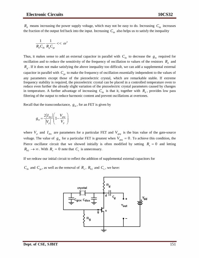
Electronic Circuits 10CS32
Dept. of CSE, SJBIT 151
Rd means increasing the power supply voltage, which may not be easy to do. Increasing Cds
increases
the fraction of the output fed back into the input. Increasing Cds also helps us to satisfy the inequality
21 1
d ds g gsR C R C
Thus, it makes sense to add an external capacitor in parallel with Cds to decrease the gm
required for
oscillation and to reduce the sensitivity of the frequency of oscillation to values of the resistors Rd and
Rg . If it does not make satisfying the above inequality too difficult, we can add a supplemental external
capacitor in parallel with Cgs to make the frequency of oscillation essentially independent to the values of
any parameters except those of the piezoelectric crystal, which are remarkable stable. If extreme
frequency stability is required, the piezoelectric crystal can be placed in a controlled temperature oven to reduce even further the already slight variation of the piezoelectric crystal parameters caused by changes
in temperature. A further advantage of increasing Cds is that it, together with Rd, provides low pass
filtering of the output to reduce harmonic content and prevent oscillations at overtones.
Recall that the transconductance, gm , for an FET is given by
21
gsqdss
m
pp
VIg
VV
where Vp and Idss are parameters for a particular FET and Vgsq is the bias value of the gate-source
voltage. The value of gm for a particular FET is greatest when Vgsq 0 . To achieve this condition, the
Pierce oscillator circuit that we showed initially is often modified by setting Rs 0 and letting
Rb2 . With Rs 0 note that Cs is unnecessary.
If we redraw our initial circuit to reflect the addition of supplemental external capacitors for
Cds and Cgs , as well as the removal of Rs , Rb2 and Cs , we have:

Electronic Circuits 10CS32
Dept. of CSE, SJBIT 152
where Cdsx and Cgsx are the supplemental external capacitors for Cds
and Cgs , respectively. This
configuration, with external capacitors, is sometimes called a Colpitts crystal oscillator, rather than a
Pierce crystal oscillator. In practice, a CMOS inverter is often substituted for the FET. Note that despite the changes, the signal equivalent circuit that we analyzed still applies, and hence all of our analysis still
holds, provided only that we replace Cdsx and Cgsx with C Cdsx dsxx and C Cgsx gsxx , respectively.

Electronic Circuits 10CS32
Dept. of CSE, SJBIT 153
6.7 Recommended Questions
1. What is positive and negative feedback?
2. What are voltage amplifier and current amplifier? Give their equivalent circuit.
3. Show that for current series feedback amplifier input and output resistances are increased
by a factor (1+Aβ) with feedback.
4. Show that for voltage shunt feedback amplifier transresistance gain, R1 and R0 are
decreased by a factor (1+Aβ) with feedback.
5. Draw the block schematic of amplifier with negative feedback.
6. Draw the circuit diagram of a current series feedback circuit and derive expression for
voltage gain and output resistance, and input resistance.
7. Draw the circuit diagram of voltage series feedback and derive expressions for input
resistance and output resistance.
8. Draw the circuit diagram of a voltage shunt feedback using BJT and derive expression for
voltage gain with feedback.
9. Draw the circuit for current shunt amplifier and justify the type of feedback. Derive the
expression for Av, β, Ri and Ro for the circuit.
10. Explain the concepts of feedback as applied to electronic amplifier circuits. What are the
advantages and disadvantages of positive and negative feedback?
11. Derive an expression for input and output resistance of a voltage shunt feedback
amplifier. (July-2007)
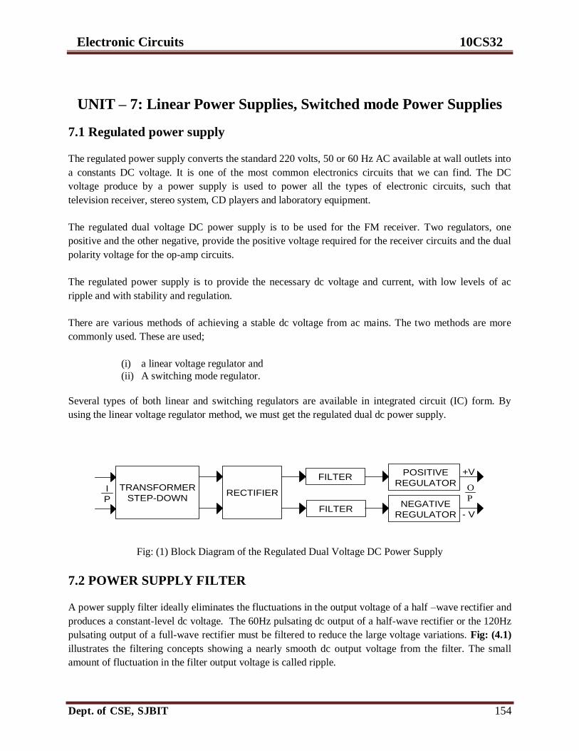
Electronic Circuits 10CS32
Dept. of CSE, SJBIT 154
UNIT – 7: Linear Power Supplies, Switched mode Power Supplies
7.1 Regulated power supply
The regulated power supply converts the standard 220 volts, 50 or 60 Hz AC available at wall outlets into
a constants DC voltage. It is one of the most common electronics circuits that we can find. The DC
voltage produce by a power supply is used to power all the types of electronic circuits, such that
television receiver, stereo system, CD players and laboratory equipment.
The regulated dual voltage DC power supply is to be used for the FM receiver. Two regulators, one
positive and the other negative, provide the positive voltage required for the receiver circuits and the dual
polarity voltage for the op-amp circuits.
The regulated power supply is to provide the necessary dc voltage and current, with low levels of ac
ripple and with stability and regulation.
There are various methods of achieving a stable dc voltage from ac mains. The two methods are more
commonly used. These are used;
(i) a linear voltage regulator and
(ii) A switching mode regulator.
Several types of both linear and switching regulators are available in integrated circuit (IC) form. By
using the linear voltage regulator method, we must get the regulated dual dc power supply.
TRANSFORMER
STEP-DOWNRECTIFIER
FILTERPOSITIVE
REGULATORO
PI
PFILTER
NEGATIVE
REGULATOR
+V
- V
Fig: (1) Block Diagram of the Regulated Dual Voltage DC Power Supply
7.2 POWER SUPPLY FILTER
A power supply filter ideally eliminates the fluctuations in the output voltage of a half –wave rectifier and
produces a constant-level dc voltage. The 60Hz pulsating dc output of a half-wave rectifier or the 120Hz
pulsating output of a full-wave rectifier must be filtered to reduce the large voltage variations. Fig: (4.1)
illustrates the filtering concepts showing a nearly smooth dc output voltage from the filter. The small
amount of fluctuation in the filter output voltage is called ripple.

Electronic Circuits 10CS32
Dept. of CSE, SJBIT 155
Vin
0 VFull-wave
RectifierFilter
0 VVout
0
Fig: (4.1) Power supply filtering
Capacitor Filter
A half wave rectifier with a capacitor filter is shown in Fig: 4.2. During the positive first quarter-circle of
the input, the diode is forward bias and presents a low resistance path, allowing the capacitor to charge to
within 0.7V of the input peak. When the input begins to decrease below its peak, the capacitor retains its
charge and the diode becomes reversed biased since the cathode is more positive than the anode. During
the remaining part of the cycle, the capacitor can discharge only through the load resistor at a rate
determines by the RLC time constant.
RLVin
+
-
+
-
+
-
+ -
0
VP(in)
t0
0t0
VP(in) – 0.7VVc
(a) Initial charging of capacitor (diode is forward-biased) happens only once when power is turn on.
RLVin
+
-
+
-
+ -
0
VP(in)
t0 0t0
Vc
t1
t1
(b) Discharging through RL after peak of positive alternation (diode is reverse biased)
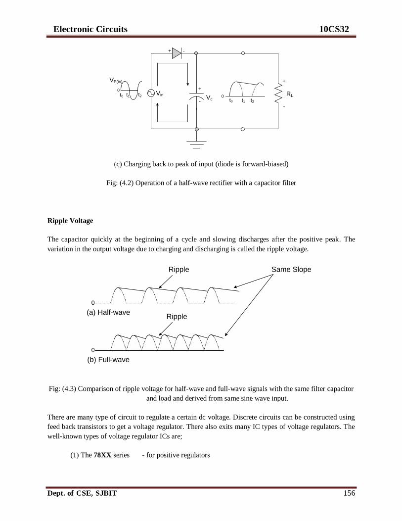
Electronic Circuits 10CS32
Dept. of CSE, SJBIT 156
RLVin
+
-
+
-
+ -
0
VP(in)
t0 0t0
Vct1
t1
t2t2
(c) Charging back to peak of input (diode is forward-biased)
Fig: (4.2) Operation of a half-wave rectifier with a capacitor filter
Ripple Voltage
The capacitor quickly at the beginning of a cycle and slowing discharges after the positive peak. The
variation in the output voltage due to charging and discharging is called the ripple voltage.
0
Ripple
(a) Half-wave
0
Ripple
(b) Full-wave
Same Slope
Fig: (4.3) Comparison of ripple voltage for half-wave and full-wave signals with the same filter capacitor
and load and derived from same sine wave input.
There are many type of circuit to regulate a certain dc voltage. Discrete circuits can be constructed using
feed back transistors to get a voltage regulator. There also exits many IC types of voltage regulators. The
well-known types of voltage regulator ICs are;
(1) The 78XX series - for positive regulators

Electronic Circuits 10CS32
Dept. of CSE, SJBIT 157
(2) The 79XX series - for negative regulators
(3) The LM 317 - for adjustable positive regulators
(4) The LM 337 - for adjustable negative regulators
7.3 Fixed Positive Linear Voltage Regulators
The 78XX series of IC regulators is representative of three terminal devices that provide a fixed positive
output voltage. The three terminals are input, output and ground as indicated in the standard fixed voltage
configuration in Fig: (5.1.a).The last two digits in the part number designate the output voltage. For
example, the ‘7805’ is a +5V regulator. Other available output voltages are given in Table: 5.1.
Capacitors although not always necessary are sometime used on the input and output as indicated in Fig:
(5.1.b). The output capacitor acts basically as a line filter to improve transient response. The input
capacitor is use to prevent unwanted oscillations when the regulator is some distance from the power
supply filter such that the line has a significant inductance.
The 78XX can produce output current in excess of 1A when used with an adequate heat sink. The 78LXX
series can provide up to 100mA, the 78MXX series can provide up to 500mA, and the 78TXX series can
provide in excess of 3A.
The input voltage must be at least 2V above the output voltage in order to maintain regulation. The
circuits have internal thermal overload protection and short-circuit current-limiting features. Thermal
overload occurs when the internal power dissipation becomes excessive and the temperature of the device
exceeds a certain value.
78XX+ INPUT + OUTPUT
IN OUT
GNDC1 C2
78XX
1 2 3
PIN 1 - INPUT
2 - GROUND
3 - OUTPUT
Fig: (5.1.a) Pin Layout Fig: (5.1.b) Standard configuration
TYPE NUMBER OUTPUT VOLTAGE
7805 +5V
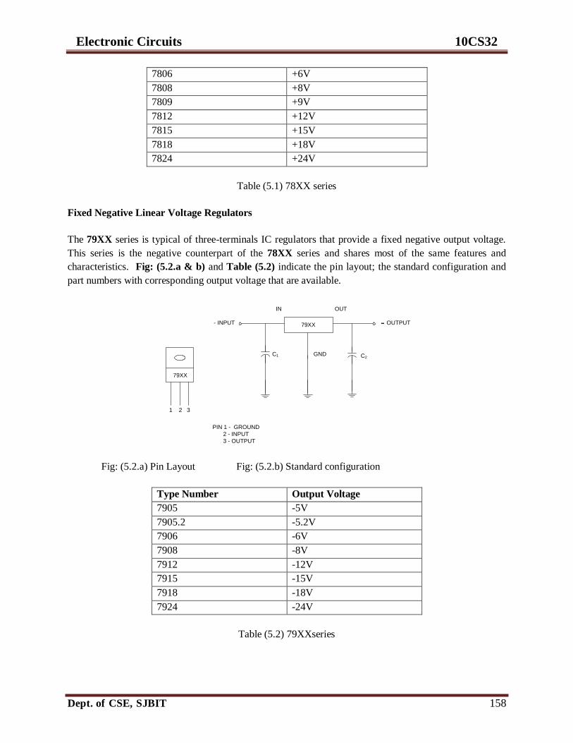
Electronic Circuits 10CS32
Dept. of CSE, SJBIT 158
7806 +6V
7808 +8V
7809 +9V
7812 +12V
7815 +15V
7818 +18V
7824 +24V
Table (5.1) 78XX series
Fixed Negative Linear Voltage Regulators
The 79XX series is typical of three-terminals IC regulators that provide a fixed negative output voltage.
This series is the negative counterpart of the 78XX series and shares most of the same features and
characteristics. Fig: (5.2.a & b) and Table (5.2) indicate the pin layout; the standard configuration and
part numbers with corresponding output voltage that are available.
79XX
1 2 3
79XX- INPUT - OUTPUT
IN OUT
GND
PIN 1 - GROUND
2 - INPUT
3 - OUTPUT
C1 C2
Fig: (5.2.a) Pin Layout Fig: (5.2.b) Standard configuration
Type Number Output Voltage
7905 -5V
7905.2 -5.2V
7906 -6V
7908 -8V
7912 -12V
7915 -15V
7918 -18V
7924 -24V
Table (5.2) 79XXseries

Electronic Circuits 10CS32
Dept. of CSE, SJBIT 159
Adjustable Positive Linear Voltage Regulators
LM317
1 2 3
PIN 1 - ADJ
2 - OUTPUT
3 - INPUT
+ OUTPUT+ INPUT IN OUT
LM317
ADJ
R2
R1VREF
IREF
Fig: (5.3.a) Pin Layout Fig: (5.3.b) Standard configuration
The LM317 is an excellent example of the three- terminal positive regulator with an adjustable output
voltage. Notice that there is an input, an output and an adjustable terminal. The external fixed resistor R1
and the external variable resistor R2 provide the output voltage adjustment. Vout can be varied from 1.2V
to 37V depending on the resistor values. The LM317 can provide over 1.5A of output current to a load.
The LM317 is operated as a “floating” regulator because the adjustment terminal is not connected to
ground, but floats to whatever voltage is across R2. This allows the output voltage to be much higher than
that of a fixed-voltage regulator.
A constant 1.25V reference voltage (VREF), is maintained by the regulator between the output terminal
and the adjustment terminal. This constant reference voltage produces a constant current (IREF) through
R1 regardless of the value of R2. IREF also flows through R2,
IREF =
11
REF
R
V25.1
R
V
2REF1REF2R1ROUT RIRIVVV
)RR(I 21REF
)RR(R
V21
1
REF

Electronic Circuits 10CS32
Dept. of CSE, SJBIT 160
)1( 2
R
RVV REFOUT
Adjustable Negative Linear Voltage Regulators
LM337
1 2 3
PIN 1 - ADJ
2 - INPUT
3 - OUTPUT
- OUTPUT- INPUT IN OUT
LM337
ADJ
R2
R1
Fig: (5.4.a) Pin Layout Fig: (5.4.b) Standard configuration
The LM 337 is the negative output counterpart of the LM 317 and is a good example of the type of IC
regulator. Like the LM 317, the LM 337 requires two external resistors for output voltage adjustments as
shown in Fig: (5.4.b). The output voltage can be adjusted from -1.2V to -37V, depending on the external
resistors values. The electrical characteristics of the LM 317 and LM 337 are shown in Table (5.4).
Parameter Conditions LM317/LM337 Units
Line Regulation TA = 25 C, 3V Vin –Vout 40V 0.04 %/V
Load Regulation TA = 25 C, 10mA Iout Imax
Vout 5V 25.00 mV
Vout 5V 0.4 %
Thermal Regulation TA = 25 C, 20ms Pulse 0.07 %/W
Adj: Pin Current 100.0 A
Reference Voltage 1.25 V
Temperature Stability Tmin Tj Tmax 1.00 %
Ripple Rejection Ratio Vout = 10V, F = 120Hz, Cadj = 10F 80.00 Db
Current Limit (Max) (VIN –VOUT 15V) 1.00 A
Current Limit (Min) (VIN –VOUT = 40V) 0.40 A
Table (5.4) Electrical Characteristics of LM 317 & LM 337

Electronic Circuits 10CS32
Dept. of CSE, SJBIT 161
7.4 The Regulated Dual Voltage DC Power Supply
By combining the step down transformer, rectifier, filters and voltage regulators together, we get a
regulated dual voltage dc power supply circuit as shown in Fig: (6.1).
Working Principle
This is a simple circuit, which gives regulated ± 1.2V to ± 15V supply. ICs LM 317T and LM 337T are
used here as positive and negative regulators respectively.
The LM 317T regulator has internal feedback regulating and current passing elements. It incorporates
various protection circuits such as current limit (which limits package power dissipation to 15 watts for
the TO-220 package) and thermal shutdown. Thus these two ICs form an independently adjustable
bipolar power supply.
Capacitors although not always necessary are sometimes used on the input and output as indicated in Fig:
(6.1). The output capacitors C7 and C8 acts basically as line filter to improve transient response. The input
capacitors C3 and C4 are used to prevent unwanted oscillations when the regulator is some distance from
the power supply filter such that the line has a significant inductance. D5 and D6 prevent short-circuit for
input and output terminals.
The TO-220 packages will easily furnish one ampere each if the heat sinks are properly mounted.
Variable resistors VR1 and VR2 are adjusted for each regulator to give a regulated output approximately
between ± 1.2V to ± 15V. Capacitors C5 and C6 are used to improve AC ripple voltage rejection.
However, if a short-circuit occurs across the regulator outputs, C5 and C6 will adjust the current in the
terminals. The output can be calculated by the formula:
)R
V1(V25.1V
1
1R0
different
d(max)L
V
PI
Circuit Diagram

Electronic Circuits 10CS32
Dept. of CSE, SJBIT 162
1
2
3
4
ADJ
IN IC2 OUT
IN IC1 OUT
ADJ
F
18V-0-18V
TRANSFORMER 1
D1 -D4
C1
C2
C3
C4
C5
C6
C7
C8
R1
R2
VR1
VR2
D5
D6
1
1
23
2 3
+ V
- V
Fig: (6.1) Circuit diagram of the regulated dual voltage DC power supply

Electronic Circuits 10CS32
Dept. of CSE, SJBIT 163
7.5 Recommended Questions
1. Design an op-amp Schmitt trigger circuit to meet the following specifications.
2. VUTP = 4V, VLTP = -2V, V= ± 12v. (July-2006)
3. Explain how an op-amp can be used as comparator.
4. Draw and explain inverting and non-inverting comparator circuits.
5. Explain op-amp is a Schmitt trigger.
6. Draw and explain the working of Schmitt trigger with different threshold levels LTP
and UTP.
7. What is integrator? Derive the expression for an output of op-amp integrator.
8. Draw and explain the basic timing circuit of IC 555. Draw the necessary waveforms.
9. Draw and explain the function block diagram of IC 555.
10. Derive the expression for the pulse width of a monostable multivibrator using IC 555.
11. Derive the expression for the frequency of the output of an astable multivibrator.
12. List the features of IC 555.
13. Draw the circuit diagram of an integrator and explain its operation with a typical
input pulse. (July-2008)
14. Draw and explain the circuit diagram of voltage controlled oscillator using the 555
timer. (July-2008)
15. Obtain an expression for the closed loop gain of anon-inverting amplifier. (July-2007)

Electronic Circuits 10CS32
Dept. of CSE, SJBIT 164
UNIT – 8: Operational Amplifier
8.1 Operational Amplifier (Op-Amp)
An operational amplifier ("op-amp") is a DC-coupled high-gain electronic voltage amplifier with a
differential input and, usually, a single-ended output. An op-amp produces an output voltage that is
typically hundreds of thousands times larger than the voltage difference between its input terminals.
Operational amplifiers are important building blocks for a wide range of electronic circuits. They had
their origins in analog computers where they were used in many linear, non-linear and frequency-
dependent circuits.
The circuit symbol for an op-amp is shown below:
Op Amp Block Diagram
The input stage is a differential amplifier. The differential amplifier used as an input stage provides
differential inputs and a frequency response down to DC. Special techniques are used to provide the high
input impedance necessary for the operational amplifier.
The second stage is a high-gain voltage amplifier. This stage may be made from several transistors to
provide high gain. A typical operational amplifier could have a voltage gain of 200,000. Most of this gain
comes from the voltage amplifier stage.
The final stage of the OP AMP is an output amplifier. The output amplifier provides low output
impedance. The actual circuit used could be an emitter follower. The output stage should allow the
operational amplifier to deliver several milliamperes to a load.
Differential
Amplifier Gain stages
Class B push-pull
output stage

Electronic Circuits 10CS32
Dept. of CSE, SJBIT 165
Notice that the operational amplifier has a positive power supply (+VCC) and a negative power supply (-
VEE). This arrangement enables the operational amplifier to produce either a positive or a negative output.
The two input terminals are labeled "inverting input" (-) and "non-inverting input" (+). The operational
amplifier can be used with three different input conditions (modes). With differential inputs (first mode),
both input terminals are used and two input signals which are 180 degrees out of phase with each other
are used. This produces an output signal that is in phase with the signal on the non-inverting input. If the
non-inverting input is grounded and a signal is applied to the inverting input (second mode), the output
signal will be 180 degrees out of phase with the input signal (and one-half the amplitude of the first mode
output). If the inverting input is grounded and a signal is applied to the non-inverting input (third mode),
the output signal will be in phase with the input signal (and one-half the amplitude of the first mode
output)
Differential Amplifier Input Stage
The differential amplifier configuration is also called as long-tail pair as the two transistors share a
common-emitter resistor. The current through this resistor is called the tail current. The base terminal of
transistor TR1 is the non-inverting input and base terminal of transistor TR2 is the inverting input. The
output is in-phase with the signal applied at non-inverting input and out-of-phase with the signal applied
at inverting input. If two different signals are applied to inverting and non-inverting inputs, the output is
given by Ad x (V1-V2)
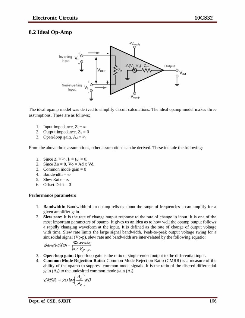
Electronic Circuits 10CS32
Dept. of CSE, SJBIT 166
8.2 Ideal Op-Amp
The ideal opamp model was derived to simplify circuit calculations. The ideal opamp model makes three
assumptions. These are as follows:
1. Input impedance, Zi = ∞
2. Output impedance, Zo = 0
3. Open-loop gain, Ad = ∞
From the above three assumptions, other assumptions can be derived. These include the following:
1. Since Zi = ∞, II = INI = 0. 2. Since Zo = 0, Vo = Ad x Vd.
3. Common mode gain = 0
4. Bandwidth = ∞
5. Slew Rate = ∞
6. Offset Drift = 0
Performance parameters
1. Bandwidth: Bandwidth of an opamp tells us about the range of frequencies it can amplify for a
given amplifier gain.
2. Slew rate: It is the rate of change output response to the rate of change in input. It is one of the most important parameters of opamp. It gives us an idea as to how well the opamp output follows
a rapidly changing waveform at the input. It is defined as the rate of change of output voltage
with time. Slew rate limits the large signal bandwidth. Peak-to-peak output voltage swing for a sinusoidal signal (Vp-p), slew rate and bandwidth are inter-related by the following equatio:
ppVSlewrate
Bandwidth
3. Open-loop gain: Open-loop gain is the ratio of single-ended output to the differential input. 4. Common Mode Rejection Ratio: Common Mode Rejection Ratio (CMRR) is a measure of the
ability of the opamp to suppress common mode signals. It is the ratio of the disered differential
gain (Ad) to the undesired common mode gain (Ac).
dBA
ACMRR
c
d
log20

Electronic Circuits 10CS32
Dept. of CSE, SJBIT 167
5. Power Supply Rejection Ratio: Power Supply Rejection Ratio (PSRR) is defined as the ratio of
change in the power supply voltage to corresponding change in the output voltage. PSRR should be zero for an Ideal opamp.
6. Input Impedance: Input Impedance (Zi) is the impedance looking into the input terminals of the
opamp and is mostly expressed in terms of resistance. Input impedance is the ratio of input
voltage to input current and is assumed to be infinite to prevent any current flowing from the source supply into the amplifiers input circuitry (Iin =0).
7. Output Impedance: Output Impedance (Zo) is defined as the impedance between the output
terminal of the opamp and ground. The output impedance of the ideal operational amplifier is assumed to be zero acting as a perfect internal voltage source with no internal resistance so that it
can supply as much current as necessary to the load. This internal resistance is effectively in
series with the load thereby reducing the output voltage available to the load. 8. Settling Time: Settling Time is a parameter specified in the case of high speed opamps of the
opamps with a high value of gain-bandwidth product
9. Offset Voltage (Vio): The amplifiers output will be zero when the voltage difference between the
inverting and the non-inverting inputs is zero, the same or when both inputs are grounded. Real
op-amps have some amount of output offset voltage.

Electronic Circuits 10CS32
Dept. of CSE, SJBIT 168
8.3 Applications of Opamp
Peak Detector Circuit
Peak Detector Circuit
Peak detector circuit produces a voltage at the output equal to peak amplitude (positive or negative) of the
input signal. It is a clipper circuit with a parallel resistor-capacitor connected at its output.
The clipper here reproduces the positive half cycles. During this period, the diode D1 is forward-biased.
The capacitor rapidly charges to the positive peak from the output of the opamp. The capacitor can now
discharge only through the resistor (R) connected across it. The value of the resistor is much larger than
the forward-biased diode‟s ON resistance. The buffer circuit connected ahead of the capacitor prevents
any discharge of the capacitor due to loading effects of the following circuit. The circuit can be made to
respond to the negative peaks by reversing the polarity of the diode.
Input / Output Waveform of Peak Detector Circuit

Electronic Circuits 10CS32
Dept. of CSE, SJBIT 169
Absolute Value Circuit
It is the configuration of opamp that produces at its output a voltage equal to the absolute value of the
input voltage. The circuit shown above is the dual half wave rectifier circuit.
When the applied input is of positive polarity (+V), diode D1 is forward biased and diode D2 is reverse
biased. The output (Vo) in this case is equal to +V.
When the applied input is of negative polarity (-V), diode D1 is reverse biased and diode D2 is forward
biased.
By applying Kirchoff‟s Current Law (KCL) at the inverting terminal of the opamp, we can determine
voltage (Vx) to be equal to
32
V. Also, Vx is related to Vo by Vx =
32
Vo. This implies that Vo = V.
Thus the output always equals the absolute value of the input signal.
Comparator
Non-inverting comparator with positive refrence and negative reference
A comparator circuit is a two input, one-output building block that produce a high or low output
depending upon the relative magnitudes of the two inputs. An opamp can be very conveniently used as a
comparator when used without negative feedback. Because of very large value of open-loop voltage gain,

Electronic Circuits 10CS32
Dept. of CSE, SJBIT 170
it produces either positively saturated or negatively saturated output voltage depending upon whether the
amplitude of the voltage applied at the non-inverting terminal is more or less positive than the voltage
applied at the inverting input terminal.
In general, reference voltage voltage may be a positive or a negative voltage. In the above figure, non-
inverting comparator with a positive reference voltage, VREF is given by
21
2
RR
RVCC
In the above figure, in the case of non-inverting comparator with a negative reference voltage,
VREF is given by
21
2
RR
RVCC
Zero Crossing Detector

Electronic Circuits 10CS32
Dept. of CSE, SJBIT 171
Non-inverting zero-crossing detector Inverting zero-crossing detector
One of the inputs of the comparator is generally applied a reference voltage and the other input is fed with
the input voltage that needs to be compared with the reference voltage. In special case where the reference
voltage is zero, the circuit is referred to as zero-crossing detector. The above figure shows inverting and
non-inverting zero crossing detector circuits with their transfer characteristics and their input / output
waveforms.
In non-inverting zero-crossing detector, input more positive than zero leads to a positively saturated
output voltage. Diodes D1 and D2 connected at the input are to protect the sensitive input circuits inside
the opamp from excessively large input voltages. In inverting zero-crossing detector, input voltage
slightly more positive than zero produces a negatively saturated output voltage. One common application
of zero-crossing detector is to convert sine wave signal to a square wave signal.
Comparator with Hysteresis

Electronic Circuits 10CS32
Dept. of CSE, SJBIT 172
The above circuit diagram shows the inverting and non-inverting comparator with hysteresis. The circuit
functions as follows.
Let us assume that the output is in positive saturation (+VSAT). voltage at non-inverting input in this case
is
21
1
RR
RVSAT
Due to this small positive voltage at the non-inverting input, the output is reinforced to stay in positive
saturation. Now, the input signal needs to be more positive than this voltage for the output to go to
negative saturation. Once the output goes to negative saturation (-VSAT), voltage fed back to non-inverting
input becomes
21
1
RR
RVSAT
A negative voltage at the non-inverting input reinforces the output to stay in negative saturation. In this
manner, the circuit offers a hysteresis of
21
12RR
RVSAT
Non-inverting comparator with hysteresis can be built by applying the input signal to the non-inverting
input as shown in the figure above. Operation is similar to that of inverting comparator. Upper and lower
trip points and hysteresis is given by
UTP = 2
1
R
RVSAT
Vo
Vi
+VSAT
-VSAT
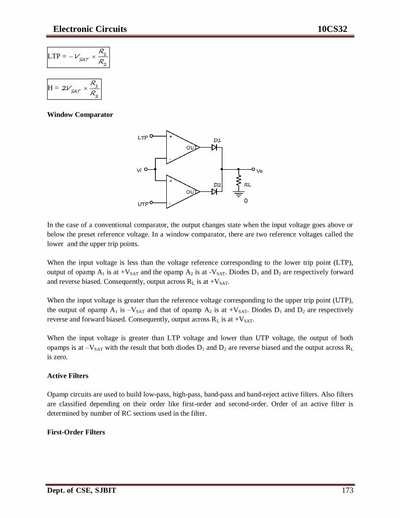
Electronic Circuits 10CS32
Dept. of CSE, SJBIT 173
LTP = 2
1
R
RVSAT
H = 2
12R
RVSAT
Window Comparator
In the case of a conventional comparator, the output changes state when the input voltage goes above or
below the preset reference voltage. In a window comparator, there are two reference voltages called the
lower and the upper trip points.
When the input voltage is less than the voltage reference corresponding to the lower trip point (LTP),
output of opamp A1 is at +VSAT and the opamp A2 is at -VSAT. Diodes D1 and D2 are respectively forward
and reverse biased. Consequently, output across RL is at +VSAT.
When the input voltage is greater than the reference voltage corresponding to the upper trip point (UTP),
the output of opamp A1 is –VSAT and that of opamp A2 is at +VSAT. Diodes D1 and D2 are respectively
reverse and forward biased. Consequently, output across RL is at +VSAT.
When the input voltage is greater than LTP voltage and lower than UTP voltage, the output of both
opamps is at –VSAT with the result that both diodes D1 and D2 are reverse biased and the output across RL
is zero.
Active Filters
Opamp circuits are used to build low-pass, high-pass, band-pass and band-reject active filters. Also filters
are classified depending on their order like first-order and second-order. Order of an active filter is
determined by number of RC sections used in the filter.
First-Order Filters

Electronic Circuits 10CS32
Dept. of CSE, SJBIT 174
The simplest low-pass and high-pass active filters are constructed by connecting lag and lead type of RC
sections, respectively, to the non-inverting inptu of the opamp wired as a voltage follower. The first order
low-pass and high-pass filters are shown in the figure below
First-order low-pass active filter First-order high-pass active filter
In the case of low-pass filter, at low frequencies, reactance offered by the capacitor is much larger than
the resistance value and therefore applied input signal appears at the output mostly unattenuated.
At high frequencies, the capacitive reactance becomes much smaller than the resistance value thus forcing
the output to be near zero.
The operation of high-pass filter can be explained as follows.
At high frequencies, reactance offered by the capacitor is much larger than the resistance value and
therefore applied input signal appears at the output mostly unattenuated.
At low frequencies, the capacitive reactance becomes much smaller than the resistance value thus forcing
the output to be near zero.
Low-pass filter with gain High-pass filter with gain
The cut-off frequency and voltage gain in both cases is given by
RCfc
21

Electronic Circuits 10CS32
Dept. of CSE, SJBIT 175
2
31RR
Av
Inverting Low-pass filter with gain Inverting High-pass filter with gain
The cut-off frequency and voltage gain in case of Inverting filters is given by
CRfc
121
1
2
R
RAv
Second Order Filters
Butterworth filter is the commonly used second order filter, it is also called as flat filter, offers a relatively
flat pass and stop band response. The generalized form of second-order Butterworth filter is shown in the
figure below.
1. If Z1 = Z2 = R and Z3 = Z4 = C, we get a second-order low-pass filter
2. If Z1 = Z2 = C and Z3 = Z4 = R, we get a second-order high-pass filter
Generalized form of second-order Butterworth filter
The cut-off frequency and pass band gain (Av) is given by

Electronic Circuits 10CS32
Dept. of CSE, SJBIT 176
RCfc
21
1
21R
RAv
Band-pass filters can be formed by cascading the high-pass and the low-pass filter sections in series.
These filters are simple to design and offer large bandwidth.
At very low frequencies, C1 and C2 offer very high reactance. As a result, the input signal is prevented
from reaching the output.
At very high frequencies, the output is shorted to the inverting input, which converts the circuit to an
inverting amplifier with zero gain. Again, there is no output.
Narrow band-pass filter
At some intermediate band of frequencies, the gain provided by the circuit offsets the loss due to potential
divider R1-R3. The resonant frequency is given by
CRQ
fR22
2
Where Q is the quality factor, for C1 = C2 = C, the quality factor and voltage gain is given by
21
3
21
2
R
RRQ
CfRQ
AR
v12
Band-reject filters can be implemented by summing together the outputs of the low-pass and
high-pass filters. These filters are simple to design and have a broad reject frequency range.

Electronic Circuits 10CS32
Dept. of CSE, SJBIT 177
Second-order Band-Reject filter
It uses a twin-T network that is connected in series with the non-inverting input of the opamp. Very low
frequency signals find their way to the output via the low-pass filter formed by R1-R2-C3. Very high
frequency signals reach the output through the high-pass filter formed by C1-C2-R3. Intermediate band of
frequencies pass through both the filters, net signal reaching the non-inverting input and hence the output
is zero. Component values are chosen by
2, 321
RRRRR CCCCC 2, 321 2140 RRR
RCfR 2
1
Phase Shifters
Phase Shifters can be used to shift the phase of the input signal over a wide range by varying Rp with 0o
and -180o being the extremes. The output lags the input by an angle
Lag-type Phase Shifter Lead-type Phase Shifter
PPCR 1tan2 PPCR 1tan2

Electronic Circuits 10CS32
Dept. of CSE, SJBIT 178
For P
P CR
1 , = 0
o For
PP C
R
1 , = 0
o
For P
P CR
1 , = -180
o For
PP C
R
1 , = 180
o
For P
P CR
1 , = -90
o For
PP C
R
1 , = 90
o
8.4 Instrumentation Amplifier
Instrumentation amplifier is a differential amplifier that has been optimized for DC performance. It is
having a high differential gain, high CMRR, high input impedance, low input offsets and low temperature
drifts.
Instrumentation amplifier
When common-mode signal is applied to Vi, ie., same positive voltage applied to both the non-inverting
inputs, voltages appearing at the output of opamps A1 and A2 and also at R1-R2 and R3-R4 junctions are
equal. A1 and A2 acts like voltage followers. In other words common-mode gain ACM of the
preamplifier stage is unity.
On the other hand, when a differential signal is applied to the input, signals appearing at two R1-R2 and
R3-R4 junctions are equal and opposite creating a virtual ground at point A. the differential gain of this
stage is therefore 1 + (R2/R1)
The differentail gain and common-mode gain of the amplifier is given by
GV R
RA 22
1 RR
ACM
2
Non-Linear Amplifier

Electronic Circuits 10CS32
Dept. of CSE, SJBIT 179
Non-Linear amplifier is the circuit, where the gain value is a non-linear function of the amplitude of the
signal applied at the input. i.e., the gain may be very large for weak input signals and very small for large
input signals, which implies that for a very large change in the amplitude of input signal, resultant change
in amplitude of output signal is very small.
For small values of input signal, diodes act as open circuit and the gain is high due to minimum
feedback. When the amplitude of input signal is large, diodes offer very small resistance and thus gain is
low.

Electronic Circuits 10CS32
Dept. of CSE, SJBIT 180
8.5 Relaxation Oscillator
Relaxation oscillator is an oscillator circuit that produces a non-sinusoidal output whose time period is
dependent on the charging time of a capacitor connected as a part of the oscillator circuit.
Let us assume that the output is initially in positive saturation. As a result, voltage at non-inverting input
of opamp is 21
1
RR
RVSAT
. This forces the output to stay in positive saturation as the capacitor C
is initially in fully discharged state. Capacitor C starts charging towards +VSAT through R.
The moment the capacitor voltage exceeds the voltage appearing at the non-inverting input, the output
switches to –VSAT. The voltage appearing at non-inverting input also changes to 21
1
RR
RVSAT
.
The capacitor starts discharging after reaching zero, it begins to discharge towards –VSAT.
Again, as soon as it becomes more negative than the negative threshold appearing at non-inverting input
of the opamp, the output switches back to +VSAT. The cycle repeats thereafter. The output is a
rectangular wave.
The expression for time period of output waveform can be derived from the exponential charging and
discharging process and is given by
11
ln2RCT
Where )( 21
1
RR
R

Electronic Circuits 10CS32
Dept. of CSE, SJBIT 181
8.6 Current-to-Voltage Converter
Current-to-Voltage converter is nothing but a transimpedance amplifier. An ideal transimoedance
amplifier makes a perfect current-to-voltage converter as it has zero input impedance ans zero output
impedance.
OL
OLio A
ARIV
1,
For AOL>>1 Vo = Ii X R
Where Zin = OLA
R1
and Zo = OL
o
AR1
8.7 Voltage-to-Current Converter
Voltage-to-Current converter is a transconductance amplifier. An in deal transconductance amplifier
makes a perfect voltage-controlled current source or a voltage-to-current converter.
OL
io
A
RRR
VI
211
, For AOL>>1, 1R
VI io

Electronic Circuits 10CS32
Dept. of CSE, SJBIT 182
Where
21
11RR
RARZ OLiin and
21
11 1
RR
RARZ OLo
8.8 Exercise Problems
Problem 1
From the circuit shown below determine the quiescent DC voltage at the collector terminal of each
transistor assuming VBE of the non-inverting transistors to be negligible. What will be the quiescent
DC value if VBE is taken at 0.7V?
Solution:-
1. Assuming VBE to be negligible, the tail current
mAR
VI
E
EET 2.1
101012
3
2. Emitter current of each transistor
mAIE 6.02102.1 3
3. Therefor, IC = IE = 0.6mA
4. Quiescent DC voltage at the collector of each transistor

Electronic Circuits 10CS32
Dept. of CSE, SJBIT 183
VRIVV CCCCCEQ 61010106.012 33
5. If VBE = 0.7V, Tail current
mAR
VVI
E
BEEET 13.1
10107.0123
6. Thus Emitter and Collector currents of each transistor is
mAI
II TCE 565.0
21013.1
2
3
7. Quiescent DC voltage at collector of each transistor is
VRIVV CCCCCEQ 35.6101010565.012 33
Problem 2
From the circuit shown below determine the cut-off frequency and the gain value at four times the
cut-off frequency.
Solution:-
1. Cut-off frequency,
kHzHzRC
fC 915.152
1010100010102
12
1 5
123
2. Gain, dBR
RAv 827.2011
)1010()10100(
11 3
3
1
2
3. Gain at cut-off point = 20.827-3 = 17.827dB
4. Gain at frequency four times the cut-off frequency will be 12 dB below the value of mid-band gain.
5. Therefore, gain at four times the cut-off frequency = 20.827-12 = 8.827 dB

Electronic Circuits 10CS32
Dept. of CSE, SJBIT 184
Problem 3
A second-order low-pass filter built around a single opamp is shown in the figure below. Calculate
the values of R1, R2, C1, C2 and R3 if the filter had a cut-off frequency of 10 kHz, Q-factor of 0.707
and input impedance not less than 10kΩ.
Solution:-
1. Q-factor is given by 2
1
21
C
CQ
2. For Q = 0.707, C1 = 2C2.
3. For input impedance of 10kΩ, R1 = 10kΩ = R2, also R3 = R1+R2, R3 = 20 kΩ
4. 212
1
CCRfC
, FCC
0011.0,210102
11010 2
23
3
5. C1 = 2C2 = 0.0022µF
8.9 Recommended Questions
1. Explain with the block diagrams, the basic types of voltage regulator circuits.
2. Compare series regulator and shunt regulator.
3. Draw neat diagram of a series regulator with fold back protection and explain its operation.
4. Explain the working principle of basic switching regulator.
5. Draw the circuit and explain the operation of step up switching regulator.
6. Draw and explain block diagram of 3 terminal IC regulator.
7. Explain the working of SAR ADC. (July 2007)
8. Explain the working R-2R ladder DAC. (July2007)
9. Explain the applications of astable multivibrator as: i) Square wave generator ii) To achieve
variable duty cycle control. (July-2007)
10. Define the terms „Load Regulation‟ and „Line Regulation‟ with respect to a power supply. (July-
2008)
11. Describe with circuit diagram, the operation of a shunt regulation power supply. (July-2008)

Electronic Circuits 10CS32
Dept. of CSE, SJBIT 185
12. What are the advantages and disadvantages of shunt regulator? What are the advantages of a
series regulator? (July-2008)
13. Explain the working of D/A converter [Binary weighted resistors] with neat sketch.
14. Draw simple sketches of IC linear regulators and IC switching regulators and compare their
characteristics.(Jan-2009)
![Vtusolution.in Electronic Circuits 10CS32 - Get Vtu notes ...vtusolution.in/.../cse-iii-electronic_circuits_[10cs32]-notes.pdf · UNIT - 5 6 Hours Large Signal ... Analog and Digital](https://img.pdfslide.us/doc/110x75/5afd4e297f8b9a256b8b67b4/electronic-circuits-10cs32-get-vtu-notes-vtusolutionincse-iii-electroniccircuits10cs32-notespdfunit.jpg)


![VTU Cse III Electronic Circuits [10cs32]](https://img.pdfslide.us/doc/110x75/5695d1bf1a28ab9b0297c28b/vtu-cse-iii-electronic-circuits-10cs32.jpg)