Embed Size (px)
Citation preview

ELECTRON TRANSPORT IN LOW DIMENSIONAL GaN/AlGaN
HETEROSTRUCTURE
A DISSERTATION
SUBMITTED TO THE DEPARTMENT OF APPLIED PHYSICS
AND THE COMMITTEE ON GRADUATE STUDIES
OF STANFORD UNIVERSITY
IN PARTIAL FULFILLMENT OF THE REQUIREMENTS
FOR THE DEGREE OF
DOCTOR OF PHILOSOPHY
Hung-Tao Chou
June 2009
UMI Number: 3363952
INFORMATION TO USERS
The quality of this reproduction is dependent upon the quality of the copy
submitted. Broken or indistinct print, colored or poor quality illustrations
and photographs, print bleed-through, substandard margins, and improper
alignment can adversely affect reproduction.
In the unlikely event that the author did not send a complete manuscript
and there are missing pages, these will be noted. Also, if unauthorized
copyright material had to be removed, a note will indicate the deletion.
®
UMI UMI Microform 3363952
Copyright 2009 by ProQuest LLC All rights reserved. This microform edition is protected against
unauthorized copying under Title 17, United States Code.
ProQuest LLC 789 East Eisenhower Parkway
P.O. Box 1346 Ann Arbor, Ml 48106-1346
© Copyright by Hung-Tao Chou 2009
All Rights Reserved
ii

I certify that I have read this dissertation and that, in my opinion, it
is fully adequate in scope and quality as a dissertation for the degree
of Doctor of Philosophy.
(David Goldhaber-Gordon) Principal Adviser
I certify that I have read this dissertation and that, in my opinion, it
is fully adequate in scope and quality as a dissertation for the degree
of Doctor of Philosophy.
(Sebastian Doniach^^^
I certify that I have read this dissertation and that, in my opinion, it
is fully adequate in scope and quality as a dissertation for the degree
of Doctor of Philosophy.
(Krishna Saraswat)
Approved for the University Committee on Graduate Studies.
iii
Abstract
Nanofabrication techniques give researchers the power to confine electrons in semi
conductors to low dimensional mesoscopic systems. The host material can be so clean
and electronically simple that we are not limited by the foibles of a particular ma
terial. Almost all interesting experiments on mesoscopic semiconductor have been
based on GaAs/AlGaAs heterostructure because of the high quality of the material,
and the fact that the electrons behave similarly to free electrons in vacuum except for
modified physical parameters (effective electron mass and g-factor, etc.). Nonetheless,
puzzles remain even for the simplest mesoscopic structures in GaAs.
By moving to a different material (GaN/AlGaN heterostructure), we can examine
the universality of the observed behaviors of GaAs-based mesoscopic systems, and we
can also probe how things change when we vary important parameters: GaN has a
higher effective mass (3X) and lower dielectric constant (0.7X) than GaAs, making
interactions more important relative to kinetic energy. GaN also has a higher g factor
(4.5X), making it easier to control spin states by applying magnetic field. In this
thesis I will present our results of transport measurement on two types of mesoscopic
system based on GaN/AlGaN:
A quasi-ID system: Quantum Point Contacts (QPC) in GaN were fabricated and
measured at low temperature. We observed well-quantized conductance plateaus, and
the plateaus split into spin-resolved plateaus at high perpendicular magnetic field. We
also observed features of 0.7 structure, an unresolved puzzle in GaAs QPGs.
A 0D system: Quantum Dots in GaN were fabricated and Coulomb blockade os
cillations of conductance were observed at low temperature. The distribution of the
IV
spacing between consecutive Coulomb Blockade Peaks reveals the statistical prop
erties of the level spacing of the confined electrons in the Quantum dot, which is
predicted to have a variation close to mean level spacing. In previous experimental
works on GaAs and Si dots, Gaussian distributions with a broad range of widths
were observed. The observation of variation greater than mean level spacing in some
GaAs and Si Quantum dot experiments has been attributed to the effect of strong
electron-electron interactions. In the GaN dot we studied here, the electron-electron
interactions are even stronger than in those previous experiments, yet we observed a
Gaussian distribution of peak spacings with a width close to the mean level spacing,
refuting the interpretation of broad variations in peak spacing in previous studies.
v
Acknowledgement
In 2001 Autumn, I left my hometown Taipei where I have lived for my whole life with
my family at that time and flew across the Pacific Ocean to study the Ph.D. program
in the United States. This eight-years journey, was full of excitement, struggles and
discovery which mostly I did not expect. Now close to the end of this journey, I really
appreciate having the privilege to spend years fulfilling my curiosity and am thankful
to many people who have played important roles in the last eight years. I would not
have reached this stage without them. I hope my words below express little of the
level of my gratitude to them.
First and foremost I would like to thank my advisor, David Goldhaber-Gordon,
who guided me into the intriguing field of mesoscopic physics. David gave me the
freedom to explore a new material system for mesoscopic physics. His optimism,
creativity, kindness, and extreme patience supported me constantly throughout my
graduate life. David listened carefully about what my goals were and tried his best
to help me achieving them. I was very lucky to have him as my advisor. What I
appreciate even more is the way David interacted with me and the insightful sugges
tions and questions he had during our discussions. He helped me to shape myself as
a scientist and develop confidence on thinking and doing research on my own.
I would like to thank Sebastian Doniach for serving on my dissertation reading
committee. Seb was also my academic advisor in Applied Physics, I enjoyed every
time talking with him and his advises were always very useful. I would also like to
thank another member of my thesis reading committee, Krishna Saraswat, who has
read my thesis chapter by chapter and gave me fruitful comments.
I would like to thank our collaborator Mike '•• Manfra for providing the highest
VI

quality of GaN/AlGAN heterostructure in the world. He also provided many useful
suggestions on fabrication techniques for GaN.
I would like to thank the group members in Goldhaber-Gordon lab. Lindsay
Moore, Gharis Quay, and I were the first three students in the group. I enjoyed
discussing physics and working with Lindsay and Charis. Always missing my family,
my first year at Stanford was quite difficult for me and I thank Lindsay and Charis
for creating a friendly and warm atmosphere in the lab. I would like to thank Ron
Potok for many late-night discussions about physics and experiments in the lab.
I had the privilege to interact with many postdocs in Goldhaber-Gordon lab and
I learned many things from them. I would like to thank Silvia Liischer for teaching
me how to use AFM and also showing me how to control instruments by Matlab.
Mark Topinka taught me many things about electronics and e-beam lithography and
helped me to build the op-amp based AC+DC adder. I would like to thank Josh Folk
for helping on my first low-temperature measurement. He taught me how to do low
noise measurement of mesoscopic devices and also gave me many suggestions on my
quantum dot measurements later on. From John Cummings I learned much knowledge
of materials and fabrication techniques. I worked with Mike Grobis for two months
on fixing the dilution refrigerator. I learned much knowledge of vacuum systems
from him. Mike was always enthusiastic about hearing other people's measurements
and I had many fruitful discussions about physics problems with him. I enjoyed
working with Benjamin Huard on graphene and I learned physics about graphene
and fabrication techniques from him. It was also a great pleasure to interact with
Sami Amasha in my last year at Stanford.
I also enjoyed interacting with the new generation of the lab, Joey Sulpizio, Mike
Jura, Ileana Rau, Andrei Garcia, Adam Sciambi and Alex Neuhausen. I had the
opportunity to work on a project of graphene with Kathryn Todd after my thesis
defense. It was a great experience working with Kathryn. I would like to thank
her for her enthusiasm and great effort on the project. I also enjoyed bouncing
experimental ideas on graphene with Nimrod Stander and Patrick Gallagher.
I would like to thank my friends who have been supporting me throughout these
years: Yu-Ju Lin, Shih-Nan Chen, Yen-Ling Liu, Chia-Wang Yeh, Yin Jay, Chuo-Ling
vii

Chang, Wen-Chin Hsu, Alice Chang and Ray Chen.
I would like to thank my auntie Michelle. She visited the United States quite often
for business, but no matter how busy she was, she always arranged dinner with me
and cheered me up. Finally, I am grateful to Carrie, my parents, my brothers Hong-
Da and Hong-Long, and my sister Lin-Hsia for their constant supports, confidence in
me, and their infinite love.
vm

Contents
Abstract iv
Acknowledgement vi
1 Introduction 1
1.1 Introduction and Motivation . . . . . . . : . . . . . . . . . . 1
1.2 Organization of this Thesis . . , - . . . . . . ' ; , . 3
2 Low dimensional mesoscopic systems 4
2.1 Two-dimensional electron gas in GaN/AIGaN heterostructure . . . . 5
2.2 Quantum Point Contacts ; . . . . . . ., . . . . 9
2.3 Quantum Dots , . , 15
2.3.1 Coulomb Blockade in Quantum dots 17
3 Devices Fabrication on GaN/AIGaN heterostructure 21
3.1 More about GaN/AIGaN heterostructure 21
3.2 Device fabrication 22
3.3 Parallel Conduction in GaN/AIGaN heterostructure . . . . . . . . . . 26
4 Quantum Point Contacts in GaN 28
4.1 Devices and Measurement set-up . . . . . . . . . . . . . . . . . . . . 29
4.2 First GaN Quantum Point Contacts 30
4.2.1 Finite bias measurement . . . . . . . ^ . . . . . . . . . . . . . 33
4.3 Second Quantum Point Contact . . . . . . . . . . . . . . . . . . . . . 38
IX
4.4 Conclusions 48
5 Quantum dots in GaN 51
5.1 Devices and Measurement set-up . 52
5.2 Accidental quantum dot in quantum point contacts . . . . . . . . . . 54
5.3 Quantum dots defined by four gates 56
6 Statistics of CB Peak Spacings in GaN Quantum dots 61
6.1 Distributions of Coulomb Blockade Peak Spacings: Theory . . . . . . 62
6.2 Distributions of Coulomb Blockade Peak Spacings: Previous Experiments 66
6.3 Experimental Results in GaN Quantum Dots . . 68
6.3.1 Device Characterization ".. . 68
6.3.2 Distributions of CB peak spacings ensembles 70
A Fabrication Details 77
A.l Cutting and Cleaning 77
A.2 Process Recipe . . . . . . 78
A.3 Characterization of Alumina deposited by ALD 82
B Estimation of electron temperature due to gate leakage 84
x

List of Tables
2.1 Comparison of physical parameters between 2DEGs in GaN/AlGaN
heterostrcuture and GaAs/AlGaAs heterosturcture . 8
XI

List of Figures
2.1 Polarization and the conduction band diagram in GaN/AlGaN het-
erostructure 6
2.2 Schematic of a QPC device with split-gate structure 10
2.3 Subband energy diagram and QPC conductance vs. gate voltage . . . 12
2.4 Schematic of QPC diagrams with different voltage bias and the 2D
conductance map with respect to source drain bias and gate bias . . . 14
2.5 Schematic of a top-gated quantum dot device . . . . . . . . . . . . . 16
2.6 Schematics of energy level diagrams of quantum a dot attached to 2D
leads and Conductance plot vs. plunger gate voltage . . . . . . . . . 20
3.1 Cross-sectional TEM micrographs of threaded dislocations in GaN. . 23
3.2 SEM micrographs of a QPC device consisted of a ^4Z203/Gate bilayer
structure. • • • 26
4.1 (a) Schematic layer structure of the heterostructure. First a thick GaN
buffer is grown on Sapphire by Hydride Vapor Phase Epitaxy (HVPE)
, and then GaN and AlGaN are grown by MBE. The HVPE growth is
done by Richard Molnar at Lincoln lab and the MBE growth is done
by Mike Manfra at Bell lab. Device fabrication and measurement are
performed by myself at Stanford. (b)Linear Conductance of the QPC
at T = 4 K. A shoulder-like plateau is observed below 2e2/h. . . . 31
xii
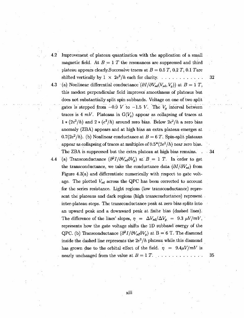
Improvement of plateau quantization with the application of a small
magnetic field. At B = 1 T the resonances are suppressed and third
plateau appears clearly.Successive traces at B = 0.5 T, 0.2 T, 0.1 Tare
shifted vertically by 1 x 2e2/h each for clarity. 32
(a) Nonlinear differential conductance (dI/dVsd(Vsd, Vg)) at B = 1 T,
this modest perpendicular field improves smoothness of plateaus but
does not substantially split spin subbands. Voltage on one of two split
gates is stepped from -0.9 Y to —1.5 V. The Vg interval between
traces is 4 mV. Plateaus in G(Vg) appear as collapsing of traces at
1 * (2e2/h) and 2 * (e2/h) around zero bias. Below 2e2/h a zero bias
anomaly (ZBA) appears and at high bias an extra plateau emerges at
0.7(2e2/h). (b) Nonlinear conductance at B — 6 T. Spin-split plateaus
appear as collapsing of traces at multiples of 0.5*(2e2//i) near zero bias.
The ZBA is suppressed but the extra plateau at high bias remains. . 3 4
(a) Transconductance (d2I/dVsddVg) at B = 1 T. In order to get
the transconductance, we take the conductance data (dI/dV3d) from
Figure 4.3(a) and differentiate numerically with respect to gate volt
age. The plotted Vsd across the QPC has been corrected to account
for the series resistance. Light regions (low transconductance) repre
sent the plateaus and dark regions (high transconductance) represent
inter-plateau steps. The transconductance peak at zero bias splits into
an upward peak and a downward peak at finite bias (dashed lines).
The difference of the lines' slopes, r? = AV^/AV^ = 9.3 jjV/mV,
represents how the gate voltage shifts the ID subband energy of the
QPC. (b) Transconductance (d2I/dVsddVg) at B = 6 T. The diamond
inside the dashed line represents the 2e2/h plateau while, this diamond
has grown due to the orbital effect of the field. 77 = 9AfjV/mV is
nearly unchanged from the value at B = 1 T. . . . . . . . . . . . . . 35
xiii
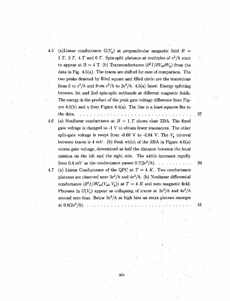
5 (a)Linear conductance G(V ,̂) at perpendicular magnetic field B =
I T , 2 T, 4 T and 6 T. Spin-split plateaus at multiples of e2/h start
to appear at B = 4 T. (b) Transconductance {d21 / dVsddVg) from the
data in Fig. 4.5(a). The traces are shifted for ease of comparison. The
two peaks denoted by filled square and filled circle are the transitions
from 0 to e2/h and from e2/h to 2e2/h. 4.5(a) Inset: Energy splitting
between 1st and 2nd spin-split subbands at different magnetic fields.
The energy is the product of the peak gate voltage difference from Fig
ure 4.5(b) and rj from Figure 4.4(a). The line is a least-squares fits to
the data
6 (a) Nonlinear conductance at B = 1 T shows clear ZBA. The fixed
gate voltage is changed to -1 V to obtain fewer resonances. The other
split-gate voltage is swept from -0.66 V to -0.84 V. The Vg interval
between traces is 4 mV. (b) Peak width of the ZBA in Figure 4.6(a)
versus gate voltage, determined as half the distance between the local
minima on the left and the right side. The width increases rapidly
from 0.4 mV as the conductance passes 0.7(2e2/h). . . .
7 (a) Linear Conductance of the QPC at T = 4 K. Two conductance
plateaus are observed near 2e2/h and 4e2/h. (b) Nonlinear differential
conductance (d2I/dVsd(Vsci, Vg)) at T — A K and zero magnetic field.
Plateaus in G(Vg) appear as collapsing of traces at 2e2/h and Ae2/h
around zero bias. Below 2e2/h at high bias an extra plateau emerges
at 0.8(2e2/h)
xiv

4.8 Numerical derivative transconductance (d2I/dVsddVg) at T = 4 K and
zero magnetic field. Darker/red regions (low transconductance) rep
resent the plateaus and yellow color regions (high transconductance)
represent inter-plateau steps. The data is blurred due to the temper
ature smearing, which becomes more clear at lower temperature[Fig
3.10(b)]. The transconductance peak at zero bias splits into an up
ward peak and a downward peak at finite bias (dashed lines). The
intersection point of Vsd between the upward line and downward line
represents the 1st subband energy of the QPC. In the plot the regions
of 0.8(2e2)//i plateau and 2e2/h plateau at high bias are surrounded
by the dashed lines 42
4.9 Linear Conductance of the QPC at T = 300 mK. For each trace, one
split gate voltage was fixed and the other gate voltage was swept. The
fixed voltage is different for each trace arid is changed from —1.5 V to
—3 V in steps of —0.1 V from left to right. The trace in the middle
(red) shows clear conductance plateaus and the trace on the right (blue)
shows oscillations in conductance 44
4.10 (a)Nonlinear differential conductance (d2I/dVsd(Vsd, Vg)) j (b) Numer
ical derivative transconductance (d2I/dVsddVg) from the data in (a).
The plotted Vsd across the QPC has been corrected to account for
the series resistance. Dark regions (low transconductance) represent
the plateaus and light regions (high transconductance) represent inter-
plateau steps. The blue dashed lines indicate the transitions from the
extra plateaus at high bias to the full plateaus. . . . . . . . . . . . . . 45
xv
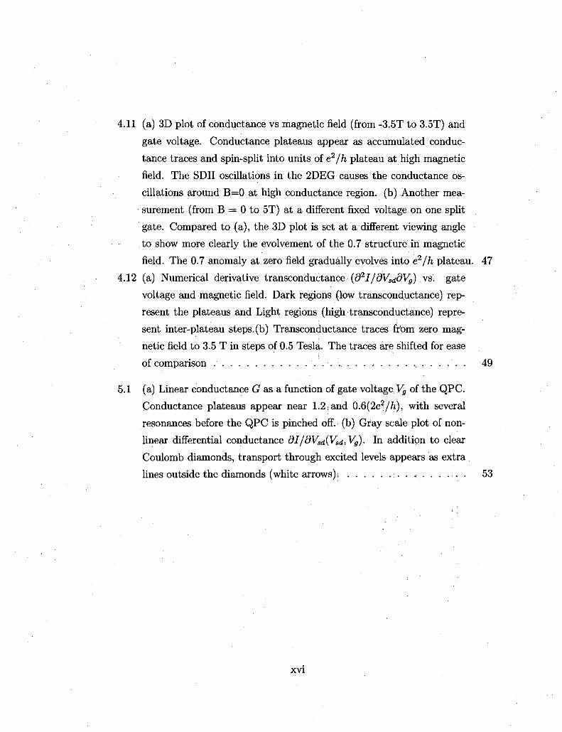
4.11 (a) 3D plot of conductance vs magnetic field (from -3.5T to 3.5T) and
gate voltage. Conductance plateaus appear as accumulated conduc
tance traces and spin-split into units of e2/h plateau at high magnetic
field. The SDH oscillations in the 2DEG causes the conductance os
cillations around B=0 at high conductance region, (b) Another mea
surement (from B = 0 to 5T) at a different fixed voltage on one split
gate. Compared to (a), the 3D plot is set at a different viewing angle
to show more clearly the evolvement of the 0.7 structure in magnetic
field. The 0.7 anomaly at zero field gradually evolves into e2/h plateau. 47
4.12 (a) Numerical derivative transconductance (d2I/dVsddVg) vs. gate
voltage and magnetic field. Dark regions (low transconductance) rep
resent the plateaus and Light regions (high transconductance) repre
sent inter-plateau steps, (b) Transconductance traces from zero mag
netic field to 3.5 T in steps of 0.5 Tesla. The traces are shifted for ease
of comparison -.. 49
5.1 (a) Linear conductance G as a function of gate voltage Vg of the QPC.
Conductance plateaus appear near 1.2 and 0.6(2e2/h), with several
resonances before the QPC is pinched off. (b) Gray scale plot of non
linear differential conductance dI/dVsd(Vsd,Vg). In addition to clear
Coulomb diamonds, transport through excited levels appears as extra
lines outside the diamonds (white arrows); . . . . . . . . . . . . . . . 53
xvi

2 Linear conductance G versus the gate voltage VG3 of the SET. Clear
Coulomb Oscillations are observed. Inset (a): Electron micrograph of
the SET. The coupling between the 2D reservoirs and the quantum
dot can be tuned by controlling the voltages on gates Gl, G2, and G4.
By varying the voltage on the plunger gate G3, the potential of the
quantum dot is modified and the energy for adding an electron to the
quantum dot is shifted into and out of resonance with the Fermi level
of the 2D reservoirs. A peak in conductance occurs when the addition
energy is aligned to the Fermi level so that an electron can tunnel onto
and off of the quantum dot. All the data shown in this section are mea
sured by varying the plunger gate G3, with gates Gl, G2, and GA fixed
at constant voltages. Inset (b): A conductance peak fit to the line-
shape expected in the classical Coulomb Blockade regime (multi-level
transport) - G = Gmax cosh_2[a(VrG3 - Vmax)/2.5kBT], where Gmax is
the peak conductance, a is the conversion ratio from gate voltage to
energy, and Vmax is the location in gate voltage of the conductance
peak. The three fit parameters are Gmaa;, Vmax, oxid rj = kBT/a. . . . 55
3 (a) Coulomb Oscillations at three different temperatures. From bottom
to top: 0.314 K, 1 K, and 3 K. '(b) The fitting parameter rj = kBT/a
as a function of temperature. The line is the least squares fit to the
data excluding the two lowest temperature points. The slope is equal
to kB/a, yielding an estimate a = 59 me V/Vg . . . . . . . . 57
4 (a) Differential conductance dI/dVsd as a function of plunger gate volt
age Vg and source-drain bias Vsd- Stable and uniform Coulomb dia-
monds are observed, (b) Energy spacing between successive adjacent
peaks. The average spacing is 0.85 meV with a fluctuation of tens of
peV < . ': • 58
1 Schematics of energy level diagrams of i quantum a dot attached to 2D
leads and CB peak plot vs. plunger gate voltage which shows the
spin-pairing effect • • • 64
xvii

2 Distributions of energy level spacings predicted by RMT. . . . . . . . . 65
3 Distribution of CB peak spacings of prior experiments 66
4 (a)Linear conductance G versus plunger gate voltage of the quantum
dot. Clear Coulomb Oscillations over a wide range of voltage were
observed, (b)Differential conductance dI/dVsd as a function of plunger
gate voltage Vg and source-drain bias Vsd- The charging energy is
« 0.86 meV estimated from the Coulomb Diamond 69
5 Inset (a) A conductance peak fit to the thermally-broadened lineshape
expected in the single-level transport regime - G = Gmax cosh_2[o:(VG—
Vmax)faksT], where Gmax is the peak conductance, a is the conver
sion ratio from gate voltage to energy, and Vmax is the location in
gate voltage of the conductance peak. The three fit parameters are
Gmax, Vmax, and V = kBT/a. (a) The fitting parameter 77 = kBT/a
(peak width) as a function of temperature. The line is the least squares
fit to the data excluding the three lowest temperature points. (b)The
inverse of the peak height (l/GTOai) as a function of temperature. . . 71
6 (a) Coulomb Blockade peak data over a wide range of gate voltage.
Each peak is fitted with a thermally-broadened lineshape and the red
dot represents the peak position and height. (b)Prom the fitting in
(a), spacing between consecutive peaks is calculated and plotted as a
function of gate voltage. To take into account the change of the dot
capacitance as gate voltage is varied, the running spacing average is
estimated by a linear fit (black line) to the spacing data, (c) Normalized
spacing after subtracting the running average spacing: 8=(AV— <
AV >)/ < AV >. . . .: . . .;..: • • • 73
7 (a)CB peak spacing distribution at zero magnetic field. The distri
bution is Gaussian-like and the standard deviation is a(B — 0) =
0.024 Ec = 1.1 ASR (b)CB peak spacing distribution at B = 50 mT.
The distribution is also Gaussian-like but has a smaller standard devi
ation a(B = 0) = 0.016 Ec = 0.75 ASR . . . . ' • . . • 74
xvin
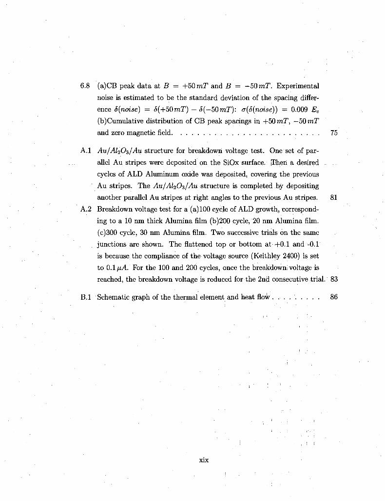
8 (a)CB peak data at B — +50 mT and B = — 50 mT. Experimental
noise is estimated to be the standard deviation of the spacing differ
ence 8(noise) = 8(+50mT) - 8(-50mT): a(S{noise)) = 0.009 Ec
(b) Cumulative distribution of CB peak spacings in +50 mT, — 50 mT
and zero magnetic field .
.1 Au/Al2Oz/Au structure for breakdown voltage: test. One set of par
allel Au stripes were deposited on the SiOx surface. Then a desired
cycles of ALD Aluminum oxide was deposited, covering the previous
Au stripes. The Au/A^O^/Au structure is completed by depositing
another parallel Au stripes at right angles to the previous Au stripes.
.2 Breakdown voltage test for a (a) 100 cycle of ALD growth, correspond
ing to a 10 nm thick Alumina film (b)200 cycle, 20 nm Alumina film.
(c)300 cycle, 30 nm Alumina film. Two successive trials on the same
junctions are shown. The flattened top or bottom at +0.1 and -Oil
is because the compliance of the voltage source (Keithley 2400) is set
to 0.1 /iA For the 100 and 200 cycles, once the breakdown; voltage is
reached, the breakdown voltage is reduced for the 2nd consecutive trial . i
.1 Schematic graph of the thermal element and heat flow . . . . . . . . .
xix
Chapter 1
Introduction
1.1 Introduction and Motivation
Nanofabrication techniques give researchers the power to confine electrons in semicon
ductors into a mesoscopic structure such as a two-dimensional (2D) quantum well, a
one-dimensional (ID) quantum wire, or a zero-dimensional (OD) quantum dot which
is sometimes referred to as an artificial atom. The host material can be so clean
and electronically simple that we are not limited by the foibles of a particular mate
rial. This emerging field is called mesoscopic physics, governing the characteristics of
the mesoscopic device with the length scale between microscopic scale of atoms and
macroscopic size of daily-life objects. It explores how electrons behave when they
are restricted to move spatially in two, one dimension or reside on a localized site
(zero-dimension). Almost all interesting experiments on mesoscopic semiconductor
structures have been based on GaAs/AlGaAs heterostructure; Reasons are: 1. High
quality of the material: in state-of-the-art GaAs/AlGaAs heterostructures electrons
can travel over hundreds of microns before totally randomizing their momentum. 2.
Advanced fabrication techniques have been developed for the past forty years. 3.
The fact that the electrons behave similarly to free electrons in vacuum except for
modified physical parameters (effective electron mass, g-factor and etc.).
In the past two decades, researchers are able to design and construct mesoscopic
system with a system size smaller than the phase coherent length, which has allowed
1

CHAPTER 1. INTRODUCTION 2
us to examine some fundamental questions about quantum mechanics, the effect
of quantum interference and also investigate the properties of a many-body system
where electron-electron interaction becomes important. For example, semiconductor
quantum dots with special spatial symmetry have been constructed and the rule for
level fillings follows patterns similar to that given by Hund's rule for a real atom[l].
Another interesting experiment, pioneered by David Goldhaber-Gordon, the realiza
tion of the Kondo model in a single electron transistor, has opened up a new research
direction in the last decade [2].
Rather than focusing on studying a mesoscopic structure with a more complicated
and advanced design, we tried to look into how the physics might change when us
ing a different material. The work presented in this thesis is focusing on exploring
the possibility of constructing and studying mesoscopic systems on Gallium Nitride
(GaN): a species of semiconductor that mesoscopic systems have never been built on.
Although many exciting mesoscopic experiments have been based on GaAs, puzzles
remain unsolved even for the simplest mesoscopic structures in GaAs. Among many
interesting puzzles, two problems which we try to investigate are the 0.7 structure in a
quantum point contact, an unexpected behavior when electrons flow through through
a partially transmitting quasi-ID system, and the statistics of, the energy level spac
ing of a chaotic quantum dot, a 0D system. We will describe these two problems
in more details in the coming chapters. These two puzzles have been discovered for
more than a decade but still remain unsettled even after efforts and trials to include
many-body effects in many different theoretical approach. An important question to
ask is that whether the puzzling phenomenons are really universal and independent
of the material.
By moving to a different material (GaN/AlGaN heterostructure), we can examine
the universality of the observed behaviors of GaAs-based mesoscopic systems, and we
can also probe how things change when we vary important parameters: GaN has a
higher effective mass (3X) and lower dielectric constant (0.7X) than GaAs, making
interactions more important relative to kinetic energy. GaN also has a higher g factor
(4.5X), making it easier to control spin states by applying magnetic field. This thesis
describes the method of device fabrication and the results of the measurement on ID

CHAPTER 1. INTRODUCTION 3
and OD system on GaN: quantum point contacts and quantum dots.
1.2 Organization of this Thesis
This chapter has provided an introduction and some motivation for the study of
mesoscopic systems in GaN. Chapter 2 gives a more detailed introduction to the
material GaN, explaining how a two dimensional electron gas (2DEG) is formed in
the GaN/AlGaN heterostructure, with a quantitative comparison of the physical pa
rameters between GaN and GaAs. It also provides a detailed background for the
lower dimensional mesoscopic system, especially quantum point contacts and quan
tum dots. Chapter 3 describes the fabrication technique, nanofabrication of GaN
mesoscopic structure, discussing the fabrication issues with this relatively new and
high quality GaN/AlGaN heterostructure and the method to solve the issues. Chap
ter 4 discusses the measurement of two GaN quantum point contacts. Chapter 5
presents results of two GaN quantum dots, one formed accidentally in a quantum
point contact and the other created with more tunability and better-defined geome
try. Chapter 6 gives a brief review for the previous experiments on statistics of level
spacings in quantum dots, and presents the results on a GaN quantum dot.
Chapter 2
Low dimensional mesoscopic
systems
What makes semiconductors a useful experimental system for mesoscopic physics is
the tunability of the system. Semiconductors can be tuned from conducting to in
sulating, from a high electron density regime where electron-electron interaction is
only a weak perturbation, to a low electron density regime where interaction and
many-body effect are important, making the ground state of the system highly cor
related. One important measure of the degree of importance of many-body effect in
a particular sample is the dimensionless interaction strength, representing the ratio
between Coulomb potential energy and kinetic energy of the electrons at the Fermi
level. The dimensionless interaction strength rs for a two dimensional system has the
form rs oc m*e/enj where e is the dielectric constant, m* is the effective mass and ns
is the 2D sheet electron density. For an electron gas with a high carrier density or a
low effective mass, the kinetic energy is large and ra << 1. Interactions can generally
be treated as a perturbation to the kinetic energy. On the other hand, ra is much
larger than 1 for an electron gas with a low carrier density of large effective mass. It
was predicted by Wigner in the extremely large rs regime, the Coulomb interaction
dominates over the kinetic energy and the electron gas tends to form an electron lat
tice or the so-called Wigner crystal to minimize the total energy[3]. Experimentally
this regime is difficult to achieve due to the requirement of the ultra-low density. The
4

CHAPTER 2. LOW DIMENSIONAL MESOSCOPIC SYSTEMS 5
mobility also becomes so low such the sample becomes highly insulating and even
making reliable ohmic contacts is challenging. In the range of rs between these two
extreme regime, many interesting two dimensional phenomena related to physics have
been discovered such as metal-insulator transition. In most of the quasi-ID and OD
dot experiments in the past, rs is ~ 1 for the two dimensional electron gas (2DEG)
where the Quantum Point Contacts (QPCs) and Quantum dots were built on. Even
with the Coulomb interaction comparable or slightly higher than the kinetic energy,
many exotic behaviors have been observed, therefore it would be interesting to explore
a QPC or a quantum dot system with a higher ra. GaN, with a larger effective mass,
generically offers a 2DEGs with a larger rs to begin with. In the remaining sections,
we shall describe how a 2DEG is formed in the AlGaN/GaN heterostructure, then
the basic transport properties of quantum point contacts and quantum dots. For
more general introductions on mesoscopic physics, the reader may refer to the book
by Davies[4] or the book by Imry[5] which has a much more sophisticated approach.
2.1 Two-dimensional electron gas in GaN/AlGaN
heterostructure
GaN is a semiconductor material with a direct band gap of 3.4 eV. Because of the wide
band gap, it has drawn recent interest in industry for use in blue laser diodes and mi
crowave power field-effect transistors. For physics studies, GaN/AlGaN heterostruc-
tures are attractive because of the rather high mobility achieved, 160000 ,cm2/Vs at
0.3if[6], and the large effective mass and g-factor. Unlike for GaAs/AlGaAs het
erostructure, no doping is needed to induce the 2DEG in GaN/AlGaN. The 2DEG in
the GaN/AlzGai-sN heterostructure arises from the discontinuity of the strong spon
taneous and piezoelectric polarization fields present at the heterojunction[7]. The
spontaneous polarization (Pse) has been attributed to the more ionic-like bonding of
GaN (A1N) and inversion asymmetry of the Wurtzite crystal structure. Due to the
strong electronegativity of Nitrogen compared to Ga and Al, the binding electron is
attracted towards N in GaN or A1N, which results in an effective dipole moment.

CHAPTER 2. LOW DIMENSIONAL MESOSCOPIC SYSTEMS 6
Surface States
Figure 2.1: (a) Schematic of the layer structure for the heterostructure and the polarization in each layer. Due to the difference of the spontaneous and piezoelectric polarization between the AlGaN and GaN layer, a positive sheet charge density exists at the interface. 2D electrons are attracted by this positive polarization and accumulate at the interface (b) Conduction band diagram along the growth z-direction. Blue line at the interface represents the ground state E0 of the triangular quantum well at the GaN/AlGaN interface.

CHAPTER 2. LOW DIMENSIONAL MESOSCOPIC SYSTEMS 7
Due to the lack of inversion symmetry of the crystal, this polarization accumulates
along certain crystal direction. The piezoelectric polarization (Ppe) is due to strain
from the lattice mismatch between the piezoelectric GaN and A^CaNi^ layer. A
higher content of Al (larger x) produces a stronger spontaneous polarization and also
a stronger lattice mismatch between Ala.GaNi_x and GaN layer, resulting in a higher
piezoelectric polarization too.
The total macroscopic polarization P is the sum of spontaneous polarization
(Pae) and piezoelectric polarization (Ppe) [Fig 2.1(a)]. The difference of the total
polarization at the interface between the Al^Ga^^N and GaN layer results in a net
polarization-induced sheet charge density. Free electrons are attracted to the inter
face between GaN and A^Gai^N to compensate this positive sheet charge density
and therefore a 2DEG is formed [7]. Where are these free electrons from? Although
this remains a unsolved question, it is generally believed these electrons are donated
by the surface states on the top Al^Gai^N layer. Figure 2.1(b) shows the conduc
tion band diagram of a GaN/A'la.Gai_a.N heterostructure along the growth direction.
Because of the built-in potential generated by the polarization field along the growth
direction, the Fermi energy of the surface states can be drawn higher than the GaN
conduction band, so that electrons could be donated from the surface states to form
the 2DEG confined by the triangular well potential at the interface. This hypothesis
has been examined and confirmed by varying the thickness of AlGaN layer[7]. It
is found that the 2DEG only emerges when the thickness passes a critical thickness,
representing a large enough built-in potential to shift energy level of the surface states
above the GaN conduction band, or more precisely, above the first quantized level
of the triangular well(blue line in Fig 2.1(b)) [8]. The fact that the 2DEG is induced
by the surface states makes the 2DEG properties very sensitive to modifications or
contaminations on sample surface.
Since the built-in potential is proportional to the thickness of the Al^Gai-^N layer
and also the polarization field, the 2DEG density can be controlled by tuning the
thickness of A^Gai^N layer and the content of the Aluminum[7]. The GaN/AlGaN
heterostructure we used are grown by our collaborator Michael Manfra at Bell Labo
ratories using molecule beam epitaxy (MBE) on GaN templates prepared by hydride
CHAPTER 2. LOW DIMENSIONAL MESOSCOPIC SYSTEMS 8
effective mass me
dielectric constant £
2D density n (m2)
Fermi wavelength XF(nm)
rs=U/EF-me/(£ni'2)
g-factor
Spin-orbit length (,7 m)
Mobility (cmWs)
Mean free path (am)
GaN
0.21
8.9
no1 6
25
2.7
2
D.3
6*104
1.Q
GaAs
0.067
12.9
3*1015
46
1.0
-0.44
4
2*106
18.0
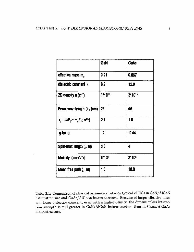
Table 2.1: Comparison of physical parameters between typical 2DEGs in GaN/AlGaN heterostrcuture and GaAs/AlGaAs heterosturcture. Because of larger effective mass and lower dielectric constant, even with a higher density, the dimensionless interaction strength is still greater in GaN/AlGaN heterostructure than in GaAs/AlGaAs heterostructure.
CHAPTER 2. LOW DIMENSIONAL MESOSCOPIC SYSTEMS 9
vapor phase epitaxy (HVPE) on sapphire [0001] substrates. The readers can find
more details in Chapter 3. Compared to a typical GaN 2DEG with a density in the
range of 1.0 x 1013 cm~2, an order lower 2DEG density ns = 1.0 x 1012 cm"2 is
achieved by using a low aluminum content of 6 percent and a thin AlGaN layer of 20
nm.
To clearly show the advantage of using GaN 2DEG, several important physical
parameters of high quality GaN and GaAs 2DEG are listed in table .2.1. Compared
to GaAs, GaN has a higher electron density (1.0 x 1012 cm~2 vs. 3.0 x 1011 cm~2),
representing a larger Fermi momentum. But the higher effective mass (0.21 vs. 0.067)
[9, 10] reduces the kinetic energy and the lower dielectric constant (8.9 vs. 12.9) in
creases the Coulomb interaction, resulting in a nearly three times larger rs (2.7 vs. 1).
The g-factor is 4.5 times larger (2 vs. 0.44) [10] in GaN than in GaAs, which makes
it easier to manipulate electron spin with magnetic field. The spin-orbit length is 300
nm in GaN [11], as where in GaAs the spin-orbit length is larger than 1 /j,m[12, 13].
For a quantum dot with a size comparable to the spin-orbit length, the spin-orbit
effect is not negligible and a ground state with a more complicated spin configura
tion could exist. With these interesting properties, one main drawback of using GaN
2DEG is the lower quality of material. The mobility is two orders lower than in a
typical high quality GaAs 2DEG. The GaN 2DEGs we have worked on have mean free
paths ranging from 0.7 to 1.5 /xm. Since the researchers are able to grow high quality
AlGaN/GaN heterostructure only since late 1990s, another drawback is the relatively
less-developed fabrication technique. Showing the ability to make a gated nanostruc-
ture in GaN/AlGaN heterostructure is most crucial and the fabrication technique will
be discussed more in next chapter.
2.2 Quantum Point Contacts
Quantum point contacts (QPCs) are quasi-one-dimensional channels connected adi-
abatically to the two-dimensional source and drain reservoirs. A general technique
to created QPCs is by gating the 2DEG with a split-gate structure on top, as shown
schematically in Fig. 2.2. In addition to the triangular well confinement along the

CHAPTER 2. LOW DIMENSIONAL MESOSCOPIC SYSTEMS 10
ex
Figure 2.2: Schematic of a QPC device with a split-gate structure. The green region represents the 2DEG. With a negative voltage Vg on two split gates, the 2DEG underneath is depleted (indicated by the black region) and current can only flow thrOugh the narrow constriction. The width of the constriction can be further reduced with a more negative Vg

CHAPTER 2. LOW DIMENSIONAL MESOSCOPIC SYSTEMS 11
heterostructure growth direction, the split-gate structure is used to create an ex
tra confinement along one direction of the plane where the 2DEG are free to move.
By negatively biasing the two surface split gates, the 2DEG underneath is depleted
and the electrons can only flow through the narrow quasi-ID constriction formed in-
between the two split gates. With a more negative biased gate voltage, the fringe
electric field repels the electrons more which causes the effective channel width to
shrink more laterally.
When the confinement caused by the gate voltage is strong enough such that
the effective channel width is comparable to the Fermi wavelength, the electron mo
tion becomes quantized along the direction parallel to the split gates (the y-direction
in Fig. 2.3(a)). When the subband spacing is much larger than the temperature,
the system should be considered as a short ID channel with a few populated sub-
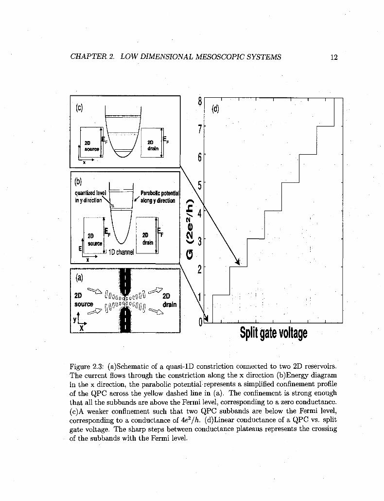
bands connected to two 2D reservoirs[Fig. 2.3(a)]. Transport measurement, a general
technique acting as energy spectroscopy in mesoscopic physics experiment, reveals
detailed properties of the mesoscopic system. As shown schematically in Fig. 2.2(a),
a small excitation AC voltage V^ is applied across the QPC, and the current flowing
across the QPC from source to drain is measured. In the non-interacting picture, each
occupied spin-degenerate subband of the QPC contributes a quantized conductance
(Go) of 2e2/h, where the factor of 2 comes from the spin degeneracy.
The energy spacing of the ID subbands is determined by the confinement potential
induced from the negatively biased split gates^ therefore the split gates can be used to
shift these ID bands up and down with respect to the Fermi level of the 2D reservoirs.
When all the ID sub-bands are higher than the 2D Fermi level [Fig 2.3(b)], electrons
can only tunnel through the QPC, resulting in a very small current flow. With a less
negative gate voltage, the subbands are shifted lower than the 2D Fermi level and
the 2D electrons with energy above the subbands can flow through the QPC. The
conductance of the QPC shows quantized plateau in mutiples of 2e2/h depending on
how many subbands are below the Fermi energy. For instance, Fig 2.3(c) represents a
QPC with two ID subbands below the 2D Fermi level, corresponding to a conductance
of 4e2//i. A sharp step between conductance plateaus [Fig 2.3(d)] is expected as each
subband crosses the 2D Fermi level one after another when the gate voltage is varied.
CHAPTER 2. LOW DIMENSIONAL MESOSCOPIC SYSTEMS 12
2D drain i
8
7
(b) quantised level inydirect ion\
Parabolic potential * along y direction
J
2D source
i
i •
\ \ F \ / \J
- 1D channel
2D drain
n—:—i 1 1 1—;—r—-T
.(d)
j i i i i_
Split gate voltage
Figure 2.3: (a)Schematic of a quasi-lD constriction connected to two 2D reservoirs. The current flows through the constriction along the x direction (b)Energy diagram in the x direction, the parabolic potential represents a simplified confinement profile of the QPC across the yellow dashed line in (a). The confinement is strong enough that all the subbands are above the Fermi level, corresponding to a zero conductance. (c)A weaker confinement such that two QPC subbands are below the Fermi level, corresponding to a conductance of 4e2/h. (d) Linear conductance of a QPC vs. split gate voltage. The sharp steps between conductance plateaus represents the crossing of the subbands with the Fermi level.
CHAPTER 2. LOW DIMENSIONAL MESOSCOPIC SYSTEMS 13
These steps are smeared out because either the 2D electrons below the subband can
tunnel through in a short QPC or higher subbands are thermally populated at a finite
temperature.
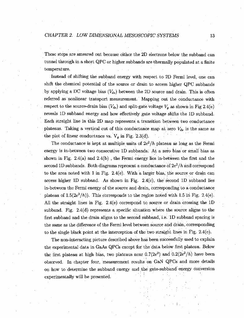
Instead of shifting the subband energy with respect to 2D Fermi level, one can
shift the chemical potential of the source or drain to access higher QPC subbands
by applying a DC voltage bias (Vds) between the 2D source and drain. This is often
referred as nonlinear transport measurement. Mapping out the conductance with
respect to the source-drain bias (Vds) and split-gate voltage Vg as shown in Fig 2.4(e)
reveals ID subband energy and how effectively gate voltage shifts the ID subband.
Each straight line in this 2D map represents a transition between two conductance
plateaus. Taking a vertical cut of this conductance map at zero Vds is the same as
the plot of linear conductance vs. Vg in Fig. 2.3(d).
The conductance is kept at multiple units of 2e2/h plateau as long as the Fermi
energy is in-between two consecutive ID subbands. At a zero bias or small bias as
shown in Fig. 2.4(a) and 2.4(b) , the Fermi energy lies in-between the first and the
second ID subbands. Both diagrams represent a conductance of 2e2/h and correspond
to the area noted with 1 in Fig. 2.4(e). With a larger bias, the source or drain can
access higher ID subband. As shown in Fig. 2.4(c), the second ID subband lies
in-between the Fermi energy of the source and drain, corresponding to a conductance
plateau of 1.5(2e2//i)). This corresponds to the region noted with 1.5 in Fig. 2.4(e).
All the straight lines in Fig. 2.4(e) correspond to source or drain crossing the ID
subband. Fig. 2.4(d) represents a specific situation where the source aligns to the
first subband and the drain aligns to the second subband, i.e. ID subband spacing is
the same as the difference of the Fermi level between source and drain, corresponding
to the single black point at the interception of the two straight lines in Fig. 2.4(e).
The non-interacting picture described above has been successfully used to explain
the experimental data in GaAs QPCs except for the data below first plateau. Below
the first plateau at high bias, two plateaus near 0.7(2e2) and 0.2(2e2//i) have been
observed. In chapter four, measurement results tin GaN QPCs and more details
on how to determine the subband energy and the gate-subband energy conversion
experimentally will be presented.
CHAPTER 2. LOW DIMENSIONAL MESOSCOPIC SYSTEMS 14
source-drain bias (VSd)
Figure 2.4: Schematic of QPC diagrams with different voltage bias and the 2D conductance map with respect to source drain bias and gate bias. (a)(b) At zero or small source drain bias such that both Fermi levels of source and drain are between latand2nd ID subband. (c) At a higher source drain bias such that Fermi level of drain is lifted above 2nd subband. (d) At a specific configuration where Fermi level of source aligns to the first subband and Fermi level of drain aligns to the 2nd subband, corresponding the blue point in (e). (e) Conductance map with respect to source drain bias and gate voltage, conductance plateaus are represented by the areas surrounded by straight lines.

CHAPTER 2. LOW DIMENSIONAL MESOSCOPIC SYSTEMS 15
2.3 Quantum Dots
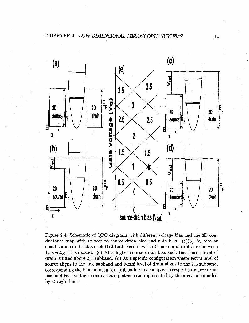
Having introduced how a QPC is formed due to the extra ID-confinement created
by the two split gates, we are now in a better position to consider how to construct
a quantum dot, electrons being confined in a small box. With analogy to the QPC,
a Quantum dot in a 2D EG can be formed by creating an extra 2D confinement. As
shown in Fig. 2.5, a small puddle of electrons can be confined in a small region
defined by the top four surrounding gates, where three gates are used to form two
QPCs in series with the quantum dot located in between. The coupling between
the 2D reservoirs and the quantum dot can be tuned by controlling the voltages on
these three gates. The size of the quantum dot is modified by varying the voltage on
the plunger gate. For a ballistic quantum dot, the dot size is larger than the Fermi
wavelength, smaller than the phase coherence length and the mean free path. In the
quantum dot discussed in this thesis, the gate pattern is designed to have hundreds
of electrons to reside on the dot, making the quantum dot a good candidate to study
many-body physics.
With a strong coupling (QPC conductance~ 2e2/h or higher), electrons can flow
through the dot via the ID subbands of the two QPCs. This is usually referred to
as the "open dot" regime. The measured conductance shows mesoscopic fluctuations
due to the quantum interference between different paths of electron flow inside the
quantum dot cavity, and this phenomenon has been used to probe the phase co
herence time. On the other hand, with the two QPCs tuned into tunneling regime
(QPC conductance below 2e2/h), electrons can only enter or exit the dot via tun
neling through the QPC barrier and the number of electrons that reside on the dot
is quantized. This is usually called the "closed dot" or "Coulomb Blockade" regime,
and the conductance of the quantum dot is below e2/h. Rather than considering
different paths inside the quantum dot, discrete energy levels and the ground state of
the quantum dot are more important. Therefore transport through quantum dots in
a "closed dot" configuration offers an ideal system to probe how many-body effects
modify the ground state of the quantum dot. In this thesis we mainly investigate
transport through quantum dots in the "closed dot" regime.
CHAPTER 2. LOW DIMENSIONAL MESOSCOPIC SYSTEMS 16
®-^D Figure 2.5: Schematic of a quantum dot device with four top gates. The green region represents the 2DEG. With a negative voltage Vg on all the gates, the 2DEG underneath is depleted (indicated by the gray region) and current can only flow through the quantum dot in-between the two 2D reservoirs.
CHAPTER 2. LOW DIMENSIONAL MESOSCOPIC SYSTEMS 17
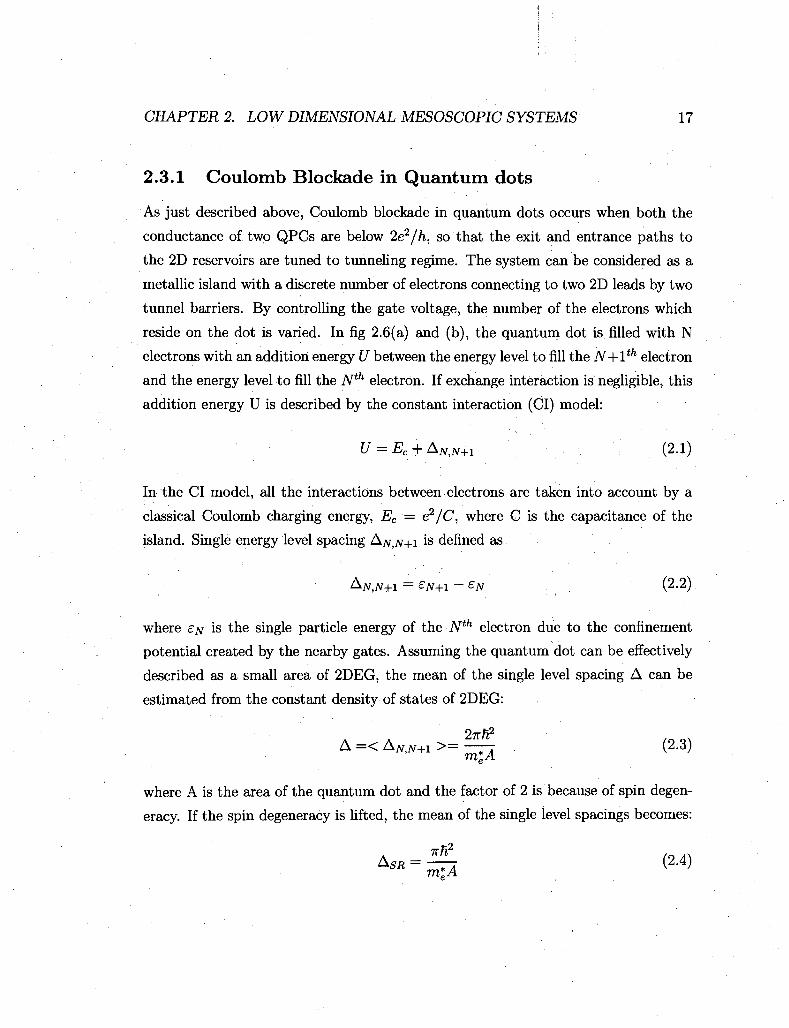
2.3.1 Coulomb Blockade in Quantum dots
As just described above, Coulomb blockade in quantum dots occurs when both the
conductance of two QPCs are below 2e2/h, so that the exit and entrance paths to
the 2D reservoirs are tuned to tunneling regime. The system can be considered as a
metallic island with a discrete number of electrons connecting to two 2D leads by two
tunnel barriers. By controlling the gate voltage, the number of the electrons which
reside on the dot is varied. In fig 2.6(a) and (b), the quantum dot is filled with N
electrons with an addition energy U between the energy level to fill the N+\th electron
and the energy level to fill the Nth electron. If exchange interaction is negligible, this
addition energy U is described by the constant interaction (CI) model:
U = Ec + AN>N+1 (2.1)
In the CI model, all the interactions between electrons are taken into account by a
classical Coulomb charging energy, Ec — e2/C, where C is the capacitance of the
island. Single energy level spacing AN>N+1 is denned as
AJV.JV+I = £N+I — £N (2.2)
where EN is the single particle energy of the •Nth electron due to the confinement
potential created by the nearby gates. Assuming the quantum dot can be effectively
described as a small area of 2DEG, the mean of the single level spacing A can be
estimated from the constant density of states of 2D EG:
A =< AJV.JV+1 >= - ^ (2.3)
m*eA
where A is the area of the quantum dot and the factor of 2 is because of spin degen
eracy. If the spin degeneracy is lifted, the mean of the single level spacings becomes:
ASR = - - : (2.4) m*eA
CHAPTER 2. LOW DIMENSIONAL MESOSCOPIC SYSTEMS 18
To observe Coulomb Blockade, one must have the temperature much smaller than
the Coulomb energy gap: kBT < ( / . A less obvious requirement is to have a discrete
set of energy levels, therefore the intrinsic level broadening should be smaller than
the mean energy level spacing, hFs, hTd -C A, where Ts andTd are the transmission
rates from the quantum dot to the source and to the drain, respectively[14].
Similar to what has been described in the previous QPC section, transport mea
surement can be used to probe the configuration of the quantum dot, as depicted in
Fig. 2.5, linear conductance is measured by applying a small AC voltage between
the 2D source and drain and measuring the current flow across the quantum dot. In
Fig. 2.6(a), the next allowed energy level of the N + 1th electron is higher than the
Fermi level of the source and drain, therefore current flow is blocked as there are only
inaccessible virtual states by which electrons can tunnel across from source to drain
through the dot, leading to the conductance valley shown in Fig. 2.6(c). By changing
the gate voltage, the levels in the dot can be capacitively tuned relative to Fermi level
of the source and drain. At a certain value of gate voltage, when there is an alignment
of a level in the dot with the 2D Fermi level as in Fig. 2.6(b), 2D electrons can tunnel
on and off the dot and the number of electrons in the ground state of the system is
fluctuated between N and N+l electrons, resulting in a current flow through the dot.
When one sweeps the gate voltage, the periodic appearance of conductance peaks
in between conductance valley at certain gate voltages is expected, as shown in Fig.
2.6(c). The valleys are referred to as "Coulomb Blockade" (CB) since the current is
blocked due to the Coulomb interaction.
The lineshape of CB conductance peak reveals the relative sizes of the different
energy scales in the system. In very low temperature where ksT <C hTs, hTd and
also ksT <C A, for simplicity we neglect the temperature effect and assume equal
coupling to the two leads(ftrs = hTd, then the CB peak is life-time broadened and
has the Breit-Wigner form
t ' ~ h {(T¥ + (EF-E0y} V ' ;
where E0 is the energy of the resonance level and T = (Fa + Td)/2

CHAPTER 2. LOW DIMENSIONAL MESOSCOPIC SYSTEMS 19
With a higher temperature where kBT » HTS, hFd and kBT < A, the peak shape
mainly depends on the thermal distribution of the 2D leads and has the form
r, GmaxA 2/EF — EQ. . . . • tn c\ G = ^TC0Sh {-2kBl^) (2'6)
where Gmax is the conductance in the high temperature limit, and EQ is the en
ergy of the resonance level. As you might have already noticed, the conductance
is temperature-dependent and therefore Coulomb Blockade is also a useful tool to
measure temperature in very low temperature regime.
CB measurement has been used to probe many different properties of quantum
dot[15, 16]. The statistics of wavefunction configuration can be probed by studying
the peak height statistics. The height of the conductance peak is related to the
coupling between the ground state of the quantum dot and the 2D leads where the
coupling is determined by the overlap between wavefunction of the OD and 2D states.
The energy spectrum of a quantum dot can be determined by measuring the spacings
between CB peaks. The gate voltage where the conductance peak appears represents
the alignment of the ground state of the quantum dot with the 2D fermi level [Fig.
2.6(b)], therefore spacing AV^ between two consecutive conductance peak is related
to the addition energy U.
U = Ec + AN,N+1 = e2/C + eN+1-eN = r)AVg, (2.7)
where -q is the conversion between gate voltage and energy. We will describe how to
extract r\ either from nonlinear transport measurement or measurement of CB peak
width vs. different temperature in chapter 4 and 5.
In few-electrons quantum dots with regular shapes, experimental results of CB
peak spacings, representing the energy spectrum of the quantum dot, have been well
described by modified Hund's rules, following the rule of shell filling. [14] In contrast
to a regular-shape dot, in chapter 6 we shall describe another regime, where the
quantum dot should be treated as a chaotic cavity and the statistics of spacing of
energy spectrum is a manifestation of Quantum Chaos.

CHAPTER 2. LOW DIMENSIONAL MESOSCOPIC SYSTEMS 20
w 0.1
-1.76 -1.72 Vg«V)
-1.6B
Figure 2.6: (a)Energy diagram of a quantum dot filled with N electrons. Fermi level of the source and drain are between allowed energy levels and current is blocked unless via in-elastic tunneling, representing a suppressed conductance valley as indicated by the arrow in (c). (b)Similar to (a) with a change in gate voltage that shifts the N+lth energy level of the dot to align with the Fermi level of source and drain, therefore current can flow through the dot via elastic tunneling, representing an enhanced conductance peak as pointed by the arrow in (c). (c)A trace of conductance vs. gate voltage taken in a GaN quantum dot. The conductance valley represents the stable configuration of quantum dot with a fixed number of electrons, as indicated by the number in the graph.

Chapter 3
Devices Fabrication on
GaN/AlGaN heterostruetlire
With no prior example of locally-gated mesoscopic devices on GaN/AIGaN het-
erostructure, working out the recipe for fabrication process is a challenging and critical
element in this project. Understanding the material properties of GaN/AlGaN het
erostructure helps to characterize and solve issues that cause device failure. In this
chapter more specific background about the GaN/AlGaN heterostructure is provided
and then more details on fabrication technique are presented. For the exact parameter
used for device fabrication, the reader may find the quantitatiye recipe in Appendix
A. ' ' . ' • ; ; '][]'. •]
3.1 More about GaN/AlGaN heterostructure
In the heterostructure we use, a 700 nm to 1 /j,m thick GaN layer followed by a 20 nm
thick AIGaN layer is grown on a GaN/Sapphire template by molecule beam epitaxy
(MBE) by our collaborator Michael Manfra at Bell Labs (now at Purdue Univer
sity). The heterojunction is formed at the GaN/AlGaN interface, 20 nm from the
top surface. The MBE process has been a powerful tool to provide the maximum low
temperature mobility because of the inherent combination of layer thickness unifor
mity, and sharp interface control and low unintentional impurity incorporation. The
2 1 • : • • ) ' ' •

CHAPTER 3. DEVICES FABRICATION ON GaN/AlGaN HETEROSTRUCTURE22
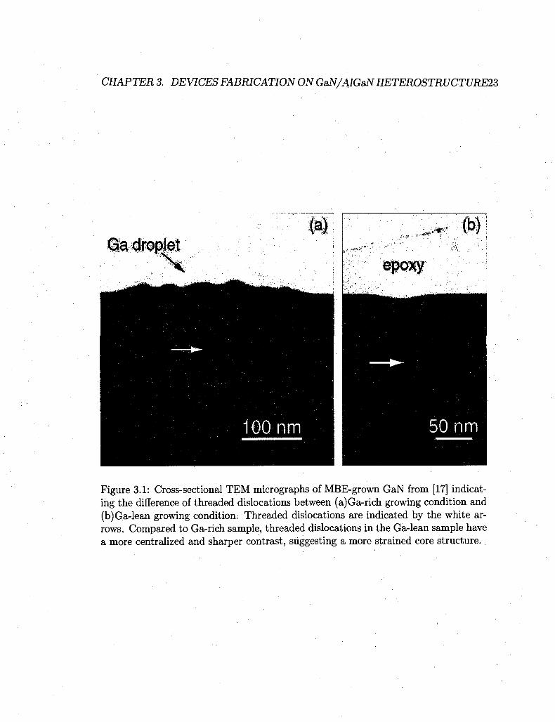
mobility in our material is mainly limited by the defects and dislocations in the tem
plate due to the lattice mismatch between the GaN and the Sapphire layer. During
the MBE growth, most dislocations in the template penetrate into the MBE grown
layer and continue all the way to the heterostructure surface [Fig. 3.1][17]. These
threaded dislocations act as the main scattering centers. To release the strain and
therefore reduce the dislocations and the defects on the GaN/Sapphire template, the
growth of the template is done by growing a very thick GaN layer (15 to 20 fim) on
the Sapphire substrate by hydride vapor phase epitaxy (HVPE). With this growth
technique, the density of the dislocations on the template can reduced to as low as
108 cm~2, corresponding to a average distance of 1 //m between dislocations[18]. This
is very close to the mean free path of the 2DEG. These threaded dislocations has also
been proved to be the main leakage path from the gates to the 2DEG[17].
3.2 Device fabrication
In order to make a working mesoscopic device, three fabrication steps have to be ful
filled. First, ohmic contacts connecting to the 2DEG with a small contact resistance.
Second, Etch to create many mesas to separate the active 2DEG region from the gate
bonding pads and also create many isolated devices on a single sample. Third, metal
gates on the surface of GaN/AlGaN heterostructure with negligible leakage current
to the 2DEG.
The GaN/AlGaN heterostructure is grown on a 2 inch diameter sapphire template.
After the MBE growth, we have to cut the wafer into small pieces in order to fit the
sample into our sample holder with a 6 mm square sample space. Since the substrate
is sapphire, it is very hard to cut the sample. One method suggested by Mike Manfra
is to scribe the back of the wafer several times by a diamond scriber, then clamp the
wafer using two glass slides and hit the wafer very hard from the back side with a
hammer. We have tried this method but ended up with several irregularly broken
pieces. Another method is to cut it using a wafersaw. We have tried to use the
wafersaw at SNF to cut the GaN wafer several times and broke the saw several times,
even after using the strongest saw at SNF suggested by SNF staffs. The final and
CHAPTER 3. DEVICES FABRICATION ON GaN/AlGaN HETEROSTRUCTURE23
Ga droplet
Figure 3.1: Cross-sectional TEM micrographs of MBE-grown GaN from [17] indicating the difference of threaded dislocations between (a)Ga-rich growing condition and (b)Ga-lean growing condition. Threaded dislocations are indicated by the white arrows. Compared to Ga-rich sample, threaded dislocations in the Ga-lean sample have a more centralized and sharper contrast, suggesting a more strained core structure.

CHAPTER 3. DEVICES FABRICATION ON GaN/AlGaN HETER0STRUCTURE1A
working solution is to ask the staff at the crystal shop in Ginzton lab or at the wafer
dicing company with a better wafersaw tool to cut the wafer. They were able to dice
the GaN wafer to regular 5 mm square pieces, though sometimes the strain building
up during the growth causes crack lines to show up on the sample after wafer dicing.
Among all the fabrication processes, making ohmic contacts is the relatively easy
step. After doing optical lithography to define the open area for the ohmic area, the
sample surface is cleaned by a buffered oxide etch (HF : H20 = 1 : 20) for one minute
before evaporating a Ti/Al (10 nm/200 nm) metal layer. After lift-off, the sample is
placed in a quartz boat and annealed at 540 °C for 15 minutes in our pre-heated tube
furnace with a flowing forming gas in an ambient environment. This method usually
gives a contact resistance less than 100 ohms for a 200 x 200 fim square ohmic pad.
Wet etching GaN is possible but it would require a more complicated procedure
such as photochemical etching by UV light activation. Instead^ our mesa etch is done
by a Chlorine-based electron cyclotron resonance (ECR) dry etch, using the PQUEST
dry etcher at SNF. The sample is heated and kept at 80 °C during etch with a etch
rate near 80 nm/minute. Sometimes two issues would show up after dry etch done
by the ECR etcher PQUEST. First is the etch surface is not uniform. In order to be
loaded into the PQUEST, the 5 mm square sample has to be attached onto a 4 inches
Si wafer by a double-sided copper tape. It is hard to level the sample well enough
which results in a non-uniform etch rate across the whole sample. Second issue is
sometimes photoresist locally gets heated too much by the bombarded plasma and
sticks on the sample surface even after immersing the sample in acetone. One way to
solve these two issues is to reduce the etch rate and the temperature, and also rotate
the sample holder during etching to improve the uniformity. The RIBE tool in KGB
lab offers all the functions just stated. Its sample holder has a electronic rotator. The
sample is kept at room temperature by a flow of cooling water and the Argon ion
beam current is much smaller such that the etch rate is only « 1 nm I minute. By
using the RIBE tool, the two issues mentioned above are both solved.
After the mesa etch, the last step is fabricating the metal gate by e-beam lithog
raphy. Two issues needs to be overcome in this step: First, due to the large stress
building up during growth, the wafer has a concave shape, and the concave geometry

CHAPTER 3. DEVICES FABRICATION ON GaN/AlGaN HETEROSTRUCTURE25
makes e-beam lithography more difficult than on a flat GaAs or Si wafer. The focus
may be quite different at two different places on a single GaN sample. Second, as men
tioned earlier threaded dislocations are the main leakage paths. Therefore preventing
the metal gate from contacting the threading dislocations is crucial for reducing the
leakage current. The concave shape problem was solved by a more brute-force way.
Rather than doing focus correction on the whole 5 mm by 5 mm sample, the focus
alignment was done on each mesa that has a smaller area (« 1 mm square). This
method gives a tolerable focus correction error. In order to reduce the leakage current,
the whole sample surface is covered by the a dielectric layer of Al2Os deposited by
atomic layer deposition (ALD) before evaporating the gate metal. By using the ALD
technique, the dielectric layer is grown monolayer by monolayer at a temperature of
100 °C, resulting in a smooth and uniform dielectric layer. The dislocations are cov
ered entirely by the ALD-grown Al203 layer. By inserting this oxide layer between
the heterostructure surface and the gate metal, leakage current is suppressed.
The low temperature growth feature of ALD makes it possible to combine the ALD
technique with lift-off defined feature by optical lithography or e-beam lithography [19].
Instead of covering the whole sample with Al203 layer that might affect the 2DEG
properties, one can do the e-beam lithography, then deposit Al203 layer and the gate
metal consecutively, and do the lift-off, resulting in the Al2Oz layer not covering the
whole sample but only underneath the gate. Since this process minimizes the time
gap between depositing Al20$ layer and gate metal, it also reduces undesired surface
scratches or contaminations that may cause gate leakage. The scanning electron mi
crograph of a QPC device is shown in Fig. 3.2. The inner layer is the metal gate layer
and the outer layer is the Al20$ layer. The larger dimension of the oxide layer is due
to the undercut of the e-beam resist and the conformal coating of ALD. In our e-beam
lithography process we use double layer of e-beam resist to produce undercut for bet
ter lift-off. After e-beam exposure and resist development, the bottom resist layer
has a wider opening than the top resist layer on the region where the resist is exposed
to electron beam, producing a nice undercut. When the A/2O3 film is deposited, due
to the isotropic and conformal coating features of ALD, the film is coated on the the
open area (GaN surface) defined by the bottom resist layer. The gate metal layer is

CHAPTER 3. DEVICES FABRICATION ON GaN/AlGaN HETEROSTRUCTURE26
Figure 3.2: SEM micrographs of a QPC device consisted of a AZ203/Gate bilayer structure. Indicated by the blue arrows is the metal gate layer; The outer layer indicated by the white arrows is the AI2O3 layer underneath the metal gate.
deposited by e-beam evaporation. The deposition is directional and thus the metal
film is deposited on top of the AI2O3 layer via the narrower window defined by the
top resist layer, resulting in a smaller dimension than the Al203 layer.
3.3 Parallel Conduction in GaN/AlGaN heterostruc-
ture
Parallel conduction is a severe and a notorious problem in the GaN/AlGaN het-
erostructure. Mesas cannot be isolated to each other if a parasitic conduction exists.
The parallel channel of conductance in the measurement also makes the data interpre
tation complicated. One source contributing to the parallel conductance is that the

CHAPTER 3. DEVICES FABRICATION ON GaN/AlGaN HETEROSTRUCTURE27
GaN template used at Bell Laboratories for MBE growth, thick HVPE films of GaN
grown on Sapphire by Dr. Richard Molnar at Lincoln Laboratory, are unintentionally
n-type doped. Residual Si has been identified as the main impurity responsible for the
n-type conductivity. This problem is solved by utilizing Zn as a deep acceptor in GaN:
the HVPE templates are doped with Zn to compensate this bulk conductivity [18],
The resulting GaN film has a bulk resistivity « 100 MQcm. The second possible
source of parallel conduction is the contaminations at the MBE/HVPE interface.
This MBE/HVPE channel is the main parallel conduction layer in the GaN/AlGaN
heterostructure we received from Bell Lab. By etching through the MBE layers
into the HVPE GaN template, the parallel conduction is eliminated between mesas,
which confirms the existence of the conduction layer at the MBE/HVPE interface.
The contaminations causing the parallel conduction is hard to control and still re
main a challenging problem to solve since it depends on the pureriess of the MBE
chamber. About three years ago we found that on a single 2 inches wafer, areas
with good isolation and areas with parallel conduction can coexist. Therefore one
cannot determine that a wafer has no parallel conduction by just testing one small
sample from it. Before realizing this coexisting problem, we generally worked with
one or two sample in one fabrication run. It takes about two weeks to fabricate, test
the device and then realize that a device with a successful lithography and lift-off is
not working due to the parallel conduction. With knowing this coexisting problem
now, we would suggest readers who want to continue on this project to switch to a
different fabrication flow: make ohmic contacts and mesas on the whole wafer first
and then find the good isolated region to use for fabrication of mesoscopic devices.
This method can save most of the fabrication and characterization time.

Chapter 4
Quantum Point Contacts in GaN
A quantum point contact (QPC) is the simplest of mesoscopic systems: a narrow
constriction between two electron reservoirs. As described in chapter 2, the width
of the constriction can be tuned so as to pass one or more channels of electrons,
each with a quantized conductance of 2e2/h (around 80 micro Siemens). The first
QPC was fabricated and measured on GaAs with well-defined; conductance plateau
in 1988[20, 21]. Yet as a QPC is just being opened up, iits conductance pauses
around 0.7(2e2/h) before rising to the first full-channel plateau. The 0.7 structure
has been one of the prime puzzles in mesoscopic physics since 1996 [22]. The shoulder
in conductance near 0.7(2e2/h) rises as temperature is lowered below 1 K, merging
into the first quantized plateau. It is generally agreed that the 0.7 structure is due
to electron interactions. In GaAs QPCs, the dimensionless interaction strength ra
has been tuned by controlling electron density to study the effect of interactions on
0.7 structure[23]. Alternatively, interaction strength can be changed by moving to a
different material system, with different dielectric constant and effective mass.
As described in chapter 2, by changing to a GaN/AlGaN heterostructure with a
larger effective mass and lower dielectric constant than in GaAs, the dimensionless
interaction strength can be made higher than that in GaAs heterostructures, even
if the 2D electron density in GaN is much higher than in GaAs. For example, rs is
70% higher for a 2DEG with density of 1012/cm2 in GaN than for the 2DEG with
a density of 1.5 x 10n/cm2 in GaAs previously used to study 0.7 structure. GaN
28

CHAPTER 4. QUANTUM POINT CONTACTS IN GaN 29
2DEGs have been created with densities as low as 2 x 10n/cm2. Quantum point
contacts on such GaN 2DEGs would have interactions four times stronger than in
typical GaAs QPCs. QPC devices have been reported in many other materials such
as SiGe[24, 25], InAs/AlSb[26], AlAs[27], and GaAs 2D hole gas[28, 29, 30, 31, 32].
GaN 2D electron gas system is similar to the GaAs 2D hole gas system where in both
system the carrier mass is larger and the spin-orbit interaction is stronger compared to
GaAs 2D electron gas system. Switching noise from the donor layer has been the main
obstacle for the QPCs in GaAs 2D hole gas system where as in GaN, the switching
noise is expected to be less because of no donor layer is required for generating the
2D electron gas.
In this chapter, we present the experiment results for two quantum point contacts
(QPC) formed in a GaN/AlGaN heterostructure. The conductance of our devices
shows well-quantized plateaus, which spin-split in high magnetic field. In addition
to the well-resolved plateaus, we also observe the '0.7' feature in conductance, which
was originally observed[22] and extensively studied in GaAs QPCs[33, 34, 35].
4.1 Devices and Measurement set-up
Each device we fabricated and measured is based on a GaN/AlGaN heterostructure.
Each heterostructure is designed to host a 2DEG 20 nm below the surface (Fig.
4.1(a). Ohmics 10 nm Ti/ 200 nm Al were annealed to contact the 2DEG. Next, a
mesa was patterned by photolithography followed by a Cl-based plasma etch. The
split-gate structure which forms the QPC was realized by electron beam lithography
followed by evaporation and lift-off of Nickel or Palladium gates. As our 2DEGs are
shallow, a high leakage current is seen when the gate metal is directly deposited on
the heterostructure surface for our early devices. To suppress leakage current from
the gates, for the 2nd QPC (data presented in section 4.3), we have used atomic layer
deposition (ALD) to form a 20 nm thick alumina layer underneath the gate. In
each device, the low temperature differential conductance dI/dVsd was measured in
a Oxford 3He system with a base temperature of 300 mK, using a lock-in technique,
with a 20 fiV excitation at 77 Hz added to a variable dc voltage Vad applied between
CHAPTER 4. QUANTUM POINT CONTACTS IN GaN 30
source and drain.
4.2 First GaN Quantum Point Contacts
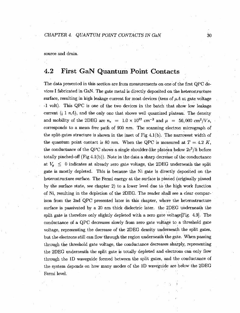
The data presented in this section are from measurements on one of the first QPC de
vices I fabricated in GaN. The gate metal is directly deposited on the heterostructure
surface, resulting in high leakage current for most devices (tens of fiA at gate voltage
-1 volt). This QPC is one of the two devices in the batch that show low leakage
current (j 1 nA), and the only one that shows well quantized plateau. The density
and mobility of the 2DEG are ns = 1.0 x 1012 cm'2 and \x = 56,000 cm2/Vs,
corresponds to a mean free path of 900 nm. The scanning electron micrograph of
the split-gates structure is shown in the inset of Fig 4.1(b). The narrowest width of
the quantum point contact is 80 nm. When the QPC is measured at T =. 4.2 K,
the conductance of the QPC shows a single shoulder-like plateau below 2e2/h before
totally pinched-off (Fig 4.1(b)). Note in the data a sharp decrease of the conductance
at Vg < 0 indicates at already zero gate voltage, the 2DEG underneath the split
gate is mostly depleted. This is because the Ni gate is directly deposited on the
heterostructure surface. The Fermi energy at the surface is pinned (originally pinned
by the surface state, see chapter 2) to a lower level due to the high work function
of Ni, resulting in the depletion of the 2DEG. The reader shall see a clear compar
ison from the 2nd QPC presented later in this chapter, where the heterostructure
surface is passivated by a 20 nm thick dielectric later, the 2DEG underneath the
split gate is therefore only slightly depleted with a zero gate voltage [Fig. 4.9]. The
conductance of a QPC decreases slowly from zero gate voltage to a threshold gate
voltage, representing the decrease of the 2DEG density underneath the split gates,
but the electrons still can flow through the region underneath the gate. When passing
through the threshold gate voltage, the conductance decreases sharply, representing
the 2DEG underneath the split gate is totally depleted and electrons can only flow
through the ID waveguide formed between the split gates, and the conductance of
the system depends on how many modes of the ID waveguide are below the 2DEG
Fermi level.

CHAPTER 4. QUANTUM POINT CONTACTS IN GaN 31
(a) GaN 3 nm cap
A lo.o6G ao.94N 1 6 n m
GaN 2 jim 2DEG
HVPE GaN 40 jum
Sapphire substrate
vgivj
Figure 4.1: (a) Schematic layer structure of the heterostructure. First a thick GaN buffer is grown on Sapphire by Hydride Vapor Phase Epitaxy (HVPE) , and then GaN and AlGaN are grown by MBE. The HVPE growth is done by Richard Molnar at Lincoln lab and the MBE growth is done by Mike Manfra at Bell lab. Device fabrication and measurement are performed by myself at Stanford. (b)Linear Conductance of the QPC at T = 4 K. A shoulder-like plateau is observed below 2e2/h.
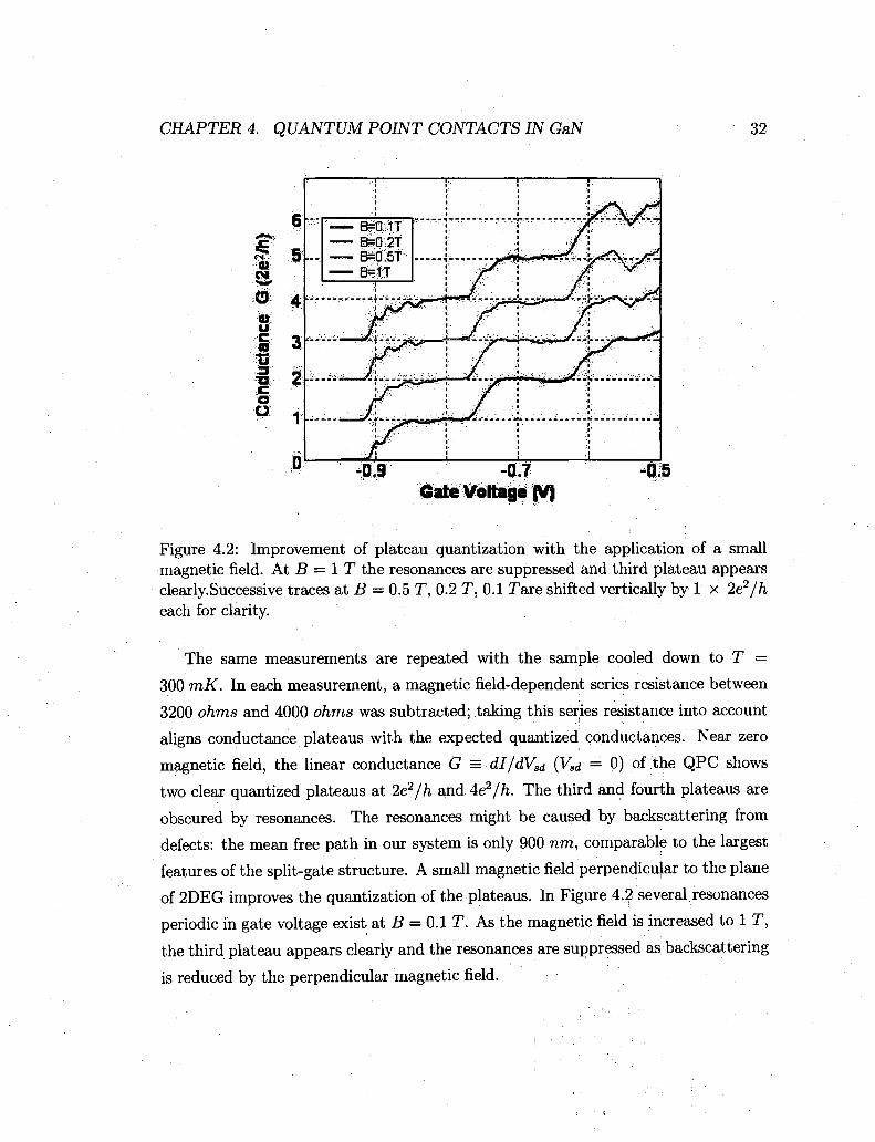
CHAPTER 4. QUANTUM POINT CONTACTS IN GaN 32
€ •
01:
01
u c 2 "G O
-a? Gate Voltage (V)
OS
Figure 4.2: Improvement of plateau quantization with the application of a small magnetic field. At B = 1 T the resonances are suppressed and third plateau appears clearly.Successive traces at B = 0.5 T, 0.2 T, 0.1 Tare shifted vertically by 1 x 2e2/h each for clarity.
The same measurements are repeated with the sample cooled down to T =
300 mK. In each measurement, a magnetic field-dependent series resistance between
3200 ohms and 4000 ohms was subtracted; taking this series resistanpe into account
aligns conductance plateaus with the expected quantized conductances. Near zero
magnetic field, the linear conductance G = dI/dVsd {Vsd = 0) of the QPC shows
two clear quantized plateaus at 2e2/h and 4e2//i. The third and fourth plateaus are
obscured by resonances. The resonances might be caused by backscattering from
defects: the mean free path in our system is only 900 nm, comparable to the largest
features of the split-gate structure. A small magnetic field perpendicular to the plane
of 2DEG improves the quantization of the plateaus. In Figure 4.2 several resonances
periodic in gate voltage exist at B = 0.1 T. As the magnetic field is increased to 1 T,
the third plateau appears clearly and the resonances are suppressed as backscattering
is reduced by the perpendicular magnetic field.
CHAPTER 4. QUANTUM POINT CONTACTS IN GaN 33
4.2.1 Finite bias measurement
Nonlinear transport measurements (dI/dVsd(Vsd,Vg)) reveal ID subband energies,
and the presence of a zero-bias anomaly (ZBA) suggests electron correlations in the
QPC (Fig. 4.3(a) and (b)). At low magnetic field B = 1 T (Fig. 4.3(a)), the
plateaus in linear conductance appear as a collapsing of traces for different gate
voltages at multiples of 2e2/h conductance when Vsd = 0. At high source-drain bias
an extra plateau appears at 0.7(2e2/h). This extra plateau is known as one of the main
features of the 0.7 structure in GaAs QPCs. The ZBA below the 2e2/h plateau has
also been observed previously in GaAs QPCs, and has been associated with a Kondo-
like correlated state that may provide a global framework for understanding the 0.7
structure[35]. At a stronger magnetic field, B = 6 T, the extra 0.7 plateau remains at
finite bias, but the ZBA is suppressed and linear conductance is quantized at e2/h =•
0.5(2e2//i) due to the large Zeeman energy - again, this agrees with observations in
GaAs QPCs.
Subband energy difference is an important parameter of a QPC, determining the
temperature and bias voltage ranges over which conductance is quantized. To measure
this value, the transconductance (d21 / dVsddVg) is plotted as a function of Vsd and
gate voltage Vg (Fig. 4.4(a) and 4.4(b)). The dashed lines are the transconductance
peaks, marking the rises between plateaus. The diamond region inside the dashed
lines is the 2e2/h plateau. The dashed lines cross at finite bias when the source is
aligned to one subband and the drain is aligned to an adjacent subband. Therefore
the crossing reveals the subband energy spacing E = eVsd, which is 2.7 meV between
the 2e2/h and 4e2/h subbands at B = 1 T. The splitting of the transconductance
peak is linear with Vsd, which means that the gate voltage affects the subband energies
linearly. Therefore we can derive a coefficient for conversion between gate voltage and
energy: 77 = AVsd/AVg = 9.3 fiV/mV(see Figure 3.4(a)). This coefficient is used in
the next section to deduce the Zeeman splitting energy.

CHAPTER 4. QUANTUM POINT CONTACTS IN GaN 34
Figure 4.3: (a) Nonlinear differential conductance (dI/dVsd(Vs<t, Vg)) at B = 1 T, this modest perpendicular field improves smoothness of plateaus but does not substantially split spin subbands. Voltage on one of two split gates is stepped from —0.9 V to —1.5 V. The Vg interval between traces is 4 mV. Plateaus in G(Vg) appear as collapsing of traces at 1 * (2e2/h) and 2 * (e2/h) around zero bias. Below 2e2/h a zero bias anomaly (ZBA) appears and at high bias an extra plateau emerges at 0.7(2e2/h). (b) Nonlinear conductance at B = 6 T. Spin-split plateaus appear as collapsing of traces at multiples of 0.5*(2e2/h) near zero bias. The ZBA is suppressed but the extra plateau at high bias remains.

CHAPTER 4. QUANTUM POINT CONTACTS IN GaN 35
>
-LO
-1 '
-1.4
.,...„ . , „ , — .
(a)
% 4e2/h •
^ ^ L
< -2e2/h
^ f c ^ _
•2 4 0 I Vsd (mV)
- 2 - 1 0 1 Vsd (mV)
Figure 4.4: (a) Transconductance (d2I/dVsddVg) at B = 1 T. In order to get the transconductance, we take the conductance data (dI/dVsd) from Figure 4.3(a) and differentiate numerically with respect to gate voltage. The plotted V3d across the QPC has been corrected to account for the series resistance. Light regions (low transconductance) represent the plateaus and dark regions (high transconductance) represent inter-plateau steps. The transconductance peak at zero bias splits into an upward peak and a downward peak at finite bias (dashed lines). The difference of the lines' slopes, 77 = AV^/AV^ = 9.3 /zV/mV, represents how the gate voltage shifts the ID subband energy of the QPC. (b) Transconductance (d2I/dVaddVg) at B = 6 T. The diamond inside the dashed line represents the 2e2/h plateau while this diamond has grown due to the orbital effect of the field, rj = 9.4/jV/mV is nearly unchanged from the value at B = 1 T.

CHAPTER 4. QUANTUM POINT CONTACTS IN GaN 36
Zeeman Splitting and Zero Bias Anomaly
A strong magnetic field induces a large Zeeman energy difference (<7/i#.B) between spin
up and spin down subbands. This energy difference results in conductance quantized
in units ote2/h rather than 2e2/h. Figure 4.5(a) shows the linear conductance G(Vg)
at four different magnetic fields which the field direction is perpendicular to the plane
of 2DEG. In addition to its effect on spin in a QPC, a perpendicular magnetic field
changes subband energies by adding an extra effective lateral confinement. This does
not alter the ID nature of transport in our QPCs, and does not further discriminate
between different spin states. Each quantized plateau simply becomes longer in higher
magnetic field because of the larger subband energy. At B = 1 T, three conductance
plateaus quantized in units of 2e2/h are observed, and a shoulder emerges below
the first plateau. At B = 4 T, spin-split plateaus (e2/h, 3e2/h,5e2/h) have already
formed, and they are more pronounced at B = 6 T. The spin-split plateaus are
due to the spin-split subbands of QPC at high magnetic field. Though our magnetic
field is perpendicular to the plane rather than in the plane of the 2DEG, the 2DEG
reservoir is in the Shubnikov-de Haas regime (v ~ 7), not the Quantum Hall regime.
Therefore, the spin-split Landau levels of the 2DEG are highly broadened and should
only have a minor contribution to the spin-split plateaus.
To deduce the Zeeman energy splitting and calculate the effective g-factor g*, we
employ the technique developed by Patel et al. [36] for GaAs QPCs. In order to get the
transconductance, we take the data from Figure 4.5(a) and differentiate numerically
(Fig. 4.5(b)). The first two peaks in Figure 4.5(b) originate from steps between
conductance plateaus: 0 to e2/h and e2/h to 2e2/h. These two peaks occur when the
spin up or spin down subband, respectively, is aligned to the Fermi level of the source
or drain. These two peaks gradually move apart as the magnetic field increases to
6 T. The energy gap between the spin-split subbands derived from these data is linear
in B but with an enhanced splitting at the lowest field 1 T (Fig. 4.5(a) inset). A
linear fit yields g* = 2.55 ± 0.05 and a zero-field offset of 0.395 ± 0.07 meV. Earlier
measurements of Shubnikov-de-Haas oscillations in a GaN 2DEG yielded a constant
g* = 2.06 up to a magnetic field of 5 Tesla[10]. Therefore our observed enhancement
of the g factor in GaN QPCs is probably due to electron-electron interactions inside

CHAPTER 4. QUANTUM POINT CONTACTS IN GaN 37
4
S3 M 0
0
(a) 1.6
•00.8
:w0.4
'/J
1 1
2 4 6 B ( T r v
i • i
i i —r
IT
Jjll.
I I I
•1.2 -0.8 Vg(V);
-0.4 •13 -11 U V g ( V ) U
Figure 4.5: (a)Linear conductance G(V )̂ at perpendicular magnetic field B = I T , 2 T, AT and 6 T. Spin-split plateaus at multiples of e2/h start to appear at B = 4 T. (b) Transconductance (d21/dVsddVg) from the data in Fig. 4.5(a). The traces are shifted for ease of comparison. The two peaks denoted by filled square and filled circle are the transitions from 0 to e2/h and from e2/h to 2e2/h. 4.5(a) Inset: Energy splitting between 1st and 2nd spin-split subbands at different magnetic fields. The energy is the product of the peak gate voltage difference from Figure 4.5(b) and r) from Figure 4.4(a). The line is a least-squares fits to the data.
CHAPTER 4. QUANTUM POINT CONTACTS IN GaN 38
the QPCs, not to exchange effects in the 2DEG at high fields. Enhancement of the
g factor and a zero field offset in subband splitting were also observed as aspects of
0.7 structure in GaAs QPCs in a parallel magnetic field measurement[22]. In the
next section the measurement of another QPC with even a stronger enhancement of
g-factor will be presented.
To further investigate the 0.7 structure in our QPCs, the channel was shifted left or
right by applying different voltages to the two split gates. The voltage difference was
adjusted to find conditions for which resonances were less pronounced, and nonlinear
transport was measured under these conditions (Fig. 4.6(a)). A more profound ZBA
emerges below the 2e2/h plateau. The width of the ZBA in Fig. 4.6(a) is shown in
Fig 4.6(b). The peak width is constant below G ~ 0.7(e2/h) and increases rapidly as
G approaches 2e2/h. The width below G ~ 0.7(2e2/h) is roughly 0.4 mV, which is
the same as the zero field energy splitting derived from the inset of Figure 4.5(a). In
GaAs, the width of a similar ZBA above G ~ 0.7(2e2//i) has been related to the Kondo
temperature of an electron trapped in the QPC [35]. The temperature dependence of
the QPC conductance reveals how strong the 0.7 structure is. Unfortunately after
a thermal cycle, warming up the QPC to room temperature and cooling it down to
300 mK again, the gates of this QPC became leaky and the device no longer showed
well-defined quantized conductance plateau. Most of the QPC devices fabricated in
the next three years show plateaus at non-integer multiples of 2e2/h accompanied
with many resonances which totally smear out the plateaus. Usually what observed
in the resonances-rich GaN QPC is quantum dot like behavior. The resonances-rich
QPC will be presented in more details in the next chapter.
4.3 Second Quantum Point Contact
Transport measurement at T — 4.2 K
After years of trial we finally were able to fabricate QPC devices that show well-
quantized plateau again. The main difference is the slightly better quality of the
2DEG properties. The density and mobility of the 2DEG are ns = 1.24 x 1012 cm'2

CHAPTER 4. QUANTUM POINT CONTACTS IN GaiV 39
0 1 Vsd (mV)
1.3
/ - \ >1.2
a v-/
50.9 T3 • H
* « , ^ 0 . 6
•a 0) ^ 0 . 3
r — 1 — r 1 1 1
I
. - • ' • • '
•
•
I
• • • • I • " • • •MM
1 { 1 1 1
-830 -805 -780 -755 -730 V g ( m V )
Figure 4.6: (a) Nonlinear conductance at B = 1 T shows clear ZBA. The fixed gate voltage is changed to -1 V to obtain fewer resonances. The other split-gate voltage is swept from -0.66 V to -0.84 V. The Vg interval between traces is 4 mV. (b) Peak width of the ZBA in Figure 4.6(a) versus gate voltage, determined as half the distance between the local minima on the left and the right side. The width increases rapidly from OAmV as the conductance passes 0.7(2e2//i).
CHAPTER 4. QUANTUM POINT CONTACTS IN GaN 40
and /J, = 84,000 cm?/Vs, corresponds to a mean free path of 1.5 fim. The longer
mean free path dramatically improves the yield of QPCs with quantized plateaus in
multiple of 2e2/h. The higher density of the 2DEG represents a higher fermi energy,
usually results in a higher subband energy of the QPC, assuming the bottom of the
potential of the QPC is the same as the 2DEG. Most QPCs fabricated from this
heterostructure show clear quantized conductance plateaus accompanied with small
resonances at 300 mK. At a higher temperature T = 4 K, the conductance shows
plateaus near 2e2/h and Ae2/h (Figure 4.7(a)). The emergence of the first two plateaus
at an elevated temperature T = 4.2 K indicates a larger subband spacing compared
to the QPC presented in the previous section. Nonlinear transport measurement
reveals ID subband energy and how the gate voltage couples to the subband energy
(Figure 4.7(b)). Besides the clear 2e2/h plateau region, at high source-drain bias an
extra plateau appears at 0.8(2e2/h), which again is a signature of 0.7 structure [23,
35]. Figure 4.8 shows the numerical derivative transconductance from the nonlinear
transport data in Figure 4.7(b). From the intersection point of the upward and
downward transconductance peak, the subband energy of 7.5 rrieV is estimated, which
is nearly three times higher than the QPC in previous section. Higher subband
energy represents sharper potential confinement and stronger electron wave function
confinement in the QPC, and the effect of electron-electron interaction should become
more prominent.
Transport measurement at T = 300 mK
When the QPC is measured at a lower temperature of T = 300 mK, higher plateaus
are resolved but small resonances emerge. To find a certain gate voltage where the
resonances are less pronounced, the channel was shifted left or right by applying
different voltages to the two split gates. Figure 4.9 shows several traces of conductance
vs. voltage of one split gate. The voltage on the other split gate; was fixed for each
trace and changed from -1.5 V to - 3 V in steps of -0.1 V from left to right.
The resonances are more pronounced for the right most (blue) trace, for the middle
traces the conductance plateaus are closer to multiples of 2e2/h. After empirically
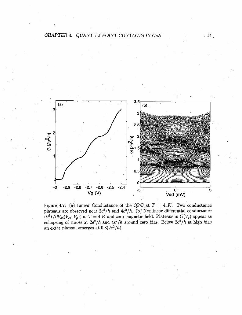
CHAPTER 4. QUANTUM POINT CONTACTS IN GaN 41
3
^ 2
O
1
I T 1 1 1 1
(a)
i i i i i i
3.5
-2.9 -2.8 -2.7 -2.6 Vg(V)
-2.5 -2.4
Vsd(mV)
Figure 4.7: (a) Linear Conductance of the QPC at T = 4 K. Two conductance plateaus are observed near 2e2/h and 4e2/h. (b) Nonlinear differential conductance (d2I/dVsd(Vsd, Vg)) at T = 4 K and zero magnetic field. Plateaus in G(Vg) appear as collapsing of traces at 2e2/h and Ae2/h around zero bias. Below 2e2/h at high bias an extra plateau emerges at 0.8(2e2//i).

CHAPTER 4. QUANTUM POINT CONTACTS IN GaN 42
Figure 4.8: Numerical derivative transconductance (d2I/dVsddVg) at T = 4 K and zero magnetic field. Darker/red regions (low transconductance) represent the plateaus and yellow color regions (high transconductance) represent inter-plateau steps. The data is blurred due to the temperature smearing, which becomes more clear at lower temperature [Fig 3.10(b)]. The transconductance peak at zero bias splits into an upward peak and a downward peak at finite bias (dashed lines). The intersection point of Vsd between the upward line and downward line represents the 1st subband energy of the QPC. In the plot the regions of 0.8(2e2)//i plateau and 2e2/h plateau at high bias are surrounded by the dashed lines.
CHAPTER 4. QUANTUM POINT CONTACTS IN GaN 43
subtracting a 1.5 kOhms series resistance for the red trace in Figure 4.9, the plateaus
in the red trace align to integer multiples of 2e2/h up to the 5th plateau (not shown
in the figure). The 20 nm thick dielectric layer of alumina deposited in-between
the heterostructure surface and the gates not only reduces the leakage current but
also prevent the metal gates from depleting the 2DEG underneath without applying
negative voltage. Using a parallel plate capacitor model, the 2DEG underneath the
gates is expected to be totally depleted when the gate voltage is —1 V. Indeed,
compared to the sharp decrease in conductance near zero gate voltage seen in Figure
4.1(b), for all the traces in Figure 4.9 the conductance remains flat in the beginning
and starts decreasing after passing Vg — — 1 V.
To search for signatures of the 0.7 structure and also to deduce the ID subband
energy, nonlinear transport measurement were made along the red color trace in
Figure 4.9 and the data are shown in Figure 4.10(a). Again, the zero bias anomaly is
observed - accompanied this time with more complicated features. The ZBA feature
of conductance at zero bias near pinch-off gradually evolves into two peaks when
approaching the first plateau. We don't have a clear explanation for this observation,
it might due to the resonances of QPC. Alternatively, a similar feature of single
conductance peak to double-peak transition was observed recently in a nonlinear
transport measurement of low density GaAs 2DEG and was attributed to a signature
of RKKY interaction [37], Future measurement of the QPC in parallel magnetic field
will be an important experiment to test wether this feature originates from RKKY
interaction.
To deduce the subband energy, numerically derived transconductance is plotted
as a function of Vsd and Vg in Figure 4.10(b). Similar to the analysis of the 1st QPC,
we estimate a subband spacing of 7 meV, 5 meV and 3 meV between the 1st and
2nd subband, 2nd and 3rd subband, and 3rd and 4th subband. The extra plateau
near 0.7(2e2//i) at high bias, another signature of 0.7 structure, shows up again in
the nonlinear transport data below the 1st subband. What's more striking is that
this behavior also emerges below the 2nd subband and 3rd subband. The transitions
from the 0.7, 1.7, 2.7 plateaus at high bias to the full plateaus represent peaks
in transconductance and are indicated by the blue dashed lines in Figure 3.10(b).

CHAPTER 4. QUANTUM POINT CONTACTS IN GaN 44
1 0
CD
- 2 - 4 - 3 . 5 - 3 - 2 . 5 - 2
V g ( V ) - 1 . 5 - 1 - 0 . 5
Figure 4.9: Linear Conductance of the QPC at T = 300 mK. For each trace, one split gate voltage was fixed and the other gate voltage was swept. The fixed voltage is different for each trace and is changed from —1.5 V to — 3 V in steps of —0.1 V from left to right. The trace in the middle (red) shows clear conductance plateaus and the trace on the right (blue) shows oscillations in conductance.
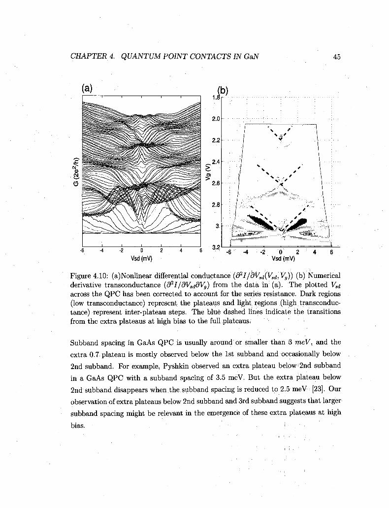
CHAPTER 4. QUANTUM POINT CONTACTS IN GaN 45
Figure 4.10: (a)Nonlinear differential conductance (d2I/idVsd(Vsd, Vg)) (b) Numerical derivative transconductance (d2I/dVsddVg) from the data in (a). The plotted Vsd across the QPC has been corrected to account for the series resistance. Dark regions (low transconductance) represent the plateaus and light regions (high transconductance) represent inter-plateau steps. The blue dashed lines indicate the transitions from the extra plateaus at high bias to the full plateaus.
Subband spacing in GaAs QPC is usually around or smaller than 3 meV, and the
extra 0.7 plateau is mostly observed below the 1st subband and occasionally below
2nd subband. For example, Pyshkin observed an extra plateau below 2nd subband
in a GaAs QPC with a subband spacing of 3.5 meV. But the extra plateau below
2nd subband disappears when the subband spacing is reduced to 2.5 meV [23]. Our
observation of extra plateaus below 2nd subband and 3rd subband suggests that larger
subband spacing might be relevant in the emergence of these extra plateaus at high
bias. ;
CHAPTER 4. QUANTUM POINT CONTACTS IN GaN 46
Zeeman Splitting in QPGs
For the 1st GaN QPC reported in the previous section we observed a slightly enhanced
g* factor of 2.5. It is generally believed that the enhancement of g* factor in a quasi-
1D system is due to exchange interaction. Calculations of the g* factor of a QPC with
a square [38] or a parabolic [39] confining potential have shown that the effective g-
factor increases when the confining potential strengthens. Recently in GaAs QPCs the
subband spacing has been tuned by modifying the gate geometry, and the observed g*
factor indeed increases with increasing subband energy[40]. In the second GaN QPC
the subband energy is about three times higher and therefore it would be interesting
to measure whether the value of g* factor is more enhanced.
In Figure 4.11 we show the 3D plot of the QPC conductance vs. gate voltage and
magnetic field. In Figure 4.11(a) the magnetic field is swept from 3.5 T to —3.5 T.
At zero magnetic field, the conductance plateaus are quantized in near units of 2e2/h.
At high magnetic field, the spin degeneracy is lifted by the Zeeman splitting and each
plateau splits into two plateaus with a e2/h difference in between. Figure 4.11(b)
shows another measurement of the QPC with the fixed split gate at a different fixed
voltage. The 0.7 structure below the 1st plateau is clear seen at zero magnetic field
and gradually evolves to a half plateau when the magnetic field is swept to 5 T.
Applying the same technique we used on the 1st QPC, we express the Zeeman
splitting as 77 x AVg for the 1st subband and 2nd subband, where 77 is the gate-energy
conversion and AV^ is the gate voltage difference between the spin-split subband.
The gate voltage on the split gates of the QPC for measurement in Figure 4.11(a) is
the same as in the nonlinear transport measurement shown in Figure 4.10, therefore
the gate-energy conversion 7? is calculated as 22.7 fj,V/mV and 11.0 nV/mV for
the 1st subband and 2nd subband from Figure 4.10(b), respectively, similar to the
method described in the caption of Figure 4.4. To identify how the plateaus split
vs magnetic field, transconductance is numerically differentiated (d2I/dVsddVg) from
the data in Figure 4.11(a) and plotted as a 2D plot vs. gate voltage and magnetic
field (Figure 4.12(a)). The light region represents higher transconductance, revealing
the transition in-between plateaus. The pair of the light regions, representing the
the spin-splitting of the subbands, evolve apart with increasing magnetic field due
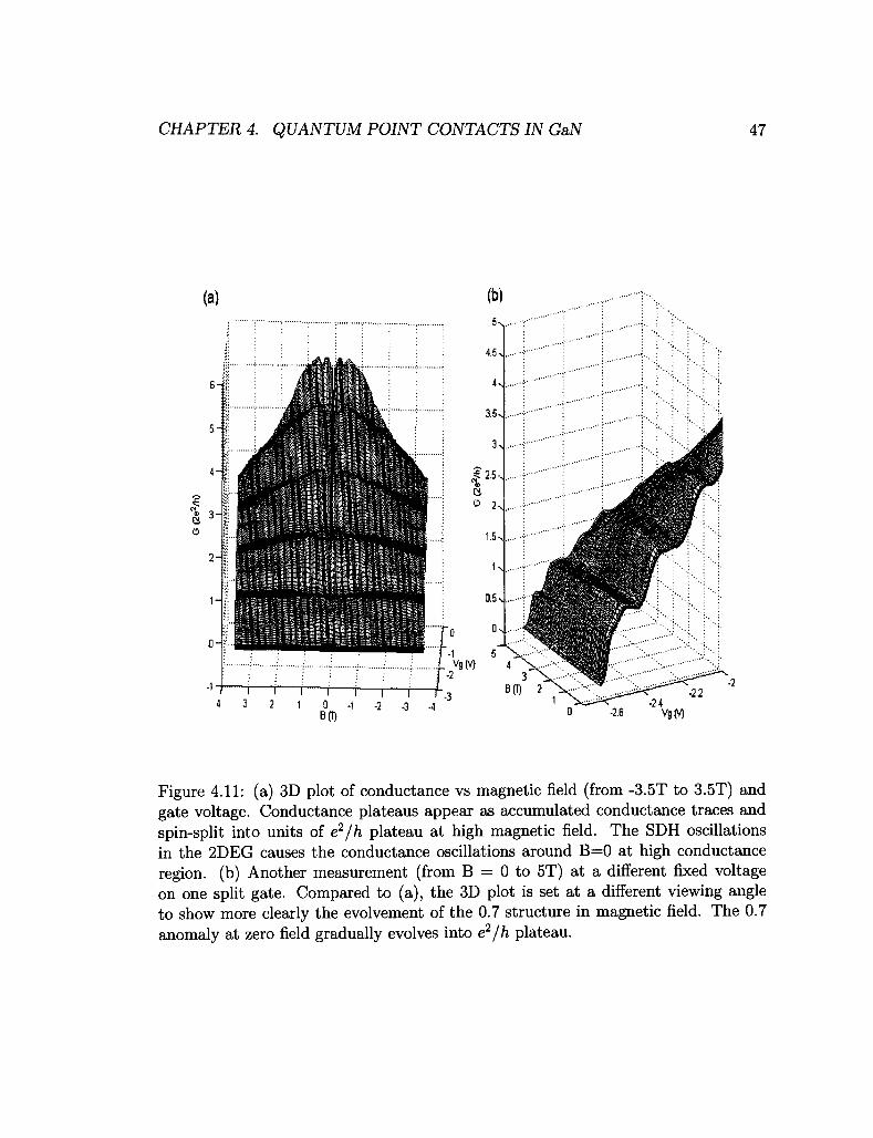
CHAPTER 4. QUANTUM POINT CONTACTS IN GaN 47
(a) (b)
Figure 4.11: (a) 3D plot of conductance vs magnetic field (from -3.5T to 3.5T) and gate voltage. Conductance plateaus appear as accumulated conductance traces and spin-split into units of e2/h plateau at high magnetic field. The SDH oscillations in the 2DEG causes the conductance oscillations around B=0 at high conductance region, (b) Another measurement (from B = 0 to 5T) at a different fixed voltage on one split gate. Compared to (a), the 3D plot is set at a different viewing angle to show more clearly the evolvement of the 0.7 structure in magnetic field. The 0.7 anomaly at zero field gradually evolves into e2/h plateau.

CHAPTER 4. QUANTUM POINT CONTACTS IN GaN 48
to the increasing Zeeman splitting. To give the reader a clearer picture, a sparse set
of transconductance traces from zero magnetic field to 3.5 T in steps of 0.5 Tesla is
plotted in Figure 4.12(b), similar to the plot in Figure 4.5(b). Zeeman splitting is
calculated from the product of the r\ and the AV^ in the figure. The g* factor is then
deduced by applying a linear fit to the Zeeman splitting with respect to magnetic field.
The g* factors are greatly enhanced and are much larger than the 2D bulk value. For
the 1st subband with a subband spacing of 7 meV, the g* factor is 11.4 ± 1.0 with a
zero-field offset of 2 meV. For the 2nd subband with a subband spacing of 5 meV,
the g* factor is 6.7 ± 0.7 with a zero-field offset of 0.4 meV. In the first QPC, the g*
factor is 2.5 for the 1st subband with a subband spacing of 2.7 meV. Therefore, in
GaN QPCs, the g* factor is strongly enhanced and increases with increasing subband
energy.
4.4 Conclusions
In this chapter we reported measurements of two GaN QPCs that show well-defined
quantized plateaus in units of 2e2/h even with a low mean free path ~ 1/zm in the
GaN 2DEG. Characteristic feature of the 0.7 anomaly-a zero bias anomaly and an
extra plateau 0.7(2e2/h) at high bias-are observed in nonlinear transport measure
ment for both QPCs at a temperature of 300 mK. For the 2nd QPC with a larger
subband spacing, appearance of extra sub-plateaus at high bias persists to the 3rd
subband. The conductance of plateaus spin-split into steps of e2/h in high magnetic
field. The g* factor is strongly enhanced and increases with increasing subband spac
ing. This agrees qualitatively with theoretic prediction. Simulations with a potential
profile closer to a real QPC device might be required to explain quantitatively our
observations.
For future work, it would be interesting to study how the geometric design of
the QPCs and higher or lower density of 2DEG affect the g* factor and the subband
spacing. If an even stronger enhancement of g* factor could be achieved by modifying
the gate geometry or 2DEG density, the GaN QPC could be utilized for spin filtering
at an elevated temperature in presence of moderate magnetic field. Since all the
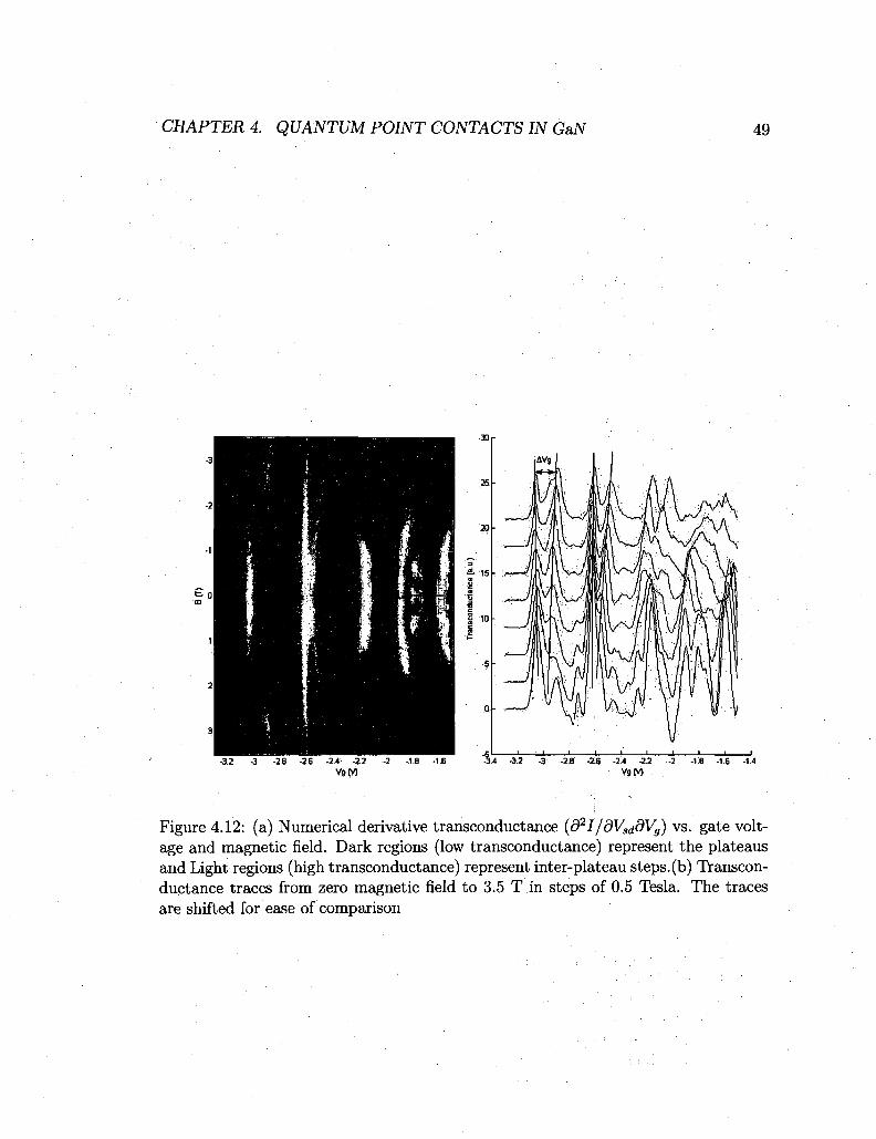
CHAPTER 4. QUANTUM POINT CONTACTS IN GaN 49
Figure 4.12: (a) Numerical derivative transconductance (d2I/dVaddVg) vs. gate voltage and magnetic field. Dark regions (low transconductance) represent the plateaus and Light regions (high transconductance) represent inter-plateau steps.(b) Transconductance traces from zero magnetic field to 3.5 T in steps of 0.5 Tesla. The traces are shifted for ease of comparison

CHAPTER 4. QUANTUM POINT CONTACTS IN GaN 50
magnetic fields in these measurements were applied perpendicularly to the QPC and
2DEG, how the in-plane magnetic field affects the transport is an interesting topic too.
In the measurements on the 2nd QPC, a lot of rich structures are observed in both
zero-field nonlinear transport and finite magnetic field. To exclude the influence of
resonances due to disorder and to study these rich structures more carefully, pursuing
high quality GaN 2DEGs with higher mean free path will be another important
research direction.
Chapter 5
Quantum dots in GaN
Semiconductor quantum dots have attracted intensive research interest in the past
two decades. The ability to tune not only energies of discrete quantum levels but also
their coupling to neighboring quantum dots or leads makes these structures a plausible
candidate for prototyping a quantum computer[41] and an excellent playground for
studying many-electron physics [42]. Most transport experiments on quantum dots
have been based on GaAs/AlGaAs heterostructures because of the mature growth
and processing technologies for this material system[14].
Our demonstration of quantum point contacts (QPCs) in GaN/AlGaN heterostruc
tures suggests that GaN would be another interesting system for exploring mesoscopic
physics. As described in chapter 2, compared to GaAs electrons in GaN have three
times higher effective mass and also 30% lower dielectric constant, increasing the
importance of electron-electron interactions relative to kinetic energy [43]. Strong
electron-electron interaction is predicted to influence mesoscopic fluctuations in closed
quantum dots, as manifested in Coulomb blockade peak-spacing statistics[15]. Elec
trons in GaN also have a larger g* factor than in GaAs and have been predicted to
have a longer spin coherence lifetime [44]. Therefore a quantum dot in GaN would be
an excellent candidate for studying many-body physics and spin physics[15, 16].
In this chapter, we report fabrication and transport studies of two GaN single
electron transistors (SETs): quantum dots coupled to conducting leads. The first SET
formed accidentally in a quantum point contact near pinchoff. Its small size produces
51

CHAPTER 5. QUANTUM DOTS IN GaN 52
large energy scales: a charging energy of 7.5 meV, and well-resolved excited states.
The second, intentionally-fabricated SET is much larger. More than one hundred
uniformly-spaced Coulomb oscillations yield a charging energy of 0.85 meV. Excited
states are not resolvable in Coulomb diamonds, and Coulomb blockade peak height
remains constant with;increasing temperature, indicating that transport is through
multiple quantum levels even at the 450 mK base electron temperature of our initial
measurements. Coulomb Oscillations of both SETs are highly stable, comparable to
the best GaAs SETs.
5.1 Devices and Measurement set-up
The devices studied in this experiment are formed in a top-gated GaN/AlGaN het-
erostructure [18, 45], whose 2DEG is only 20 nm below the surface, with density
na — 8.0 x 1011 cm~2 and mobility \x — 80,000 cm2/Vs. The method of fabricating
the device is very similar to that used for the first QPC in previous chapter, with one
additional step. Our 2DEG is very shallow, resulting in high leakage current when
gate metal is directly deposited on the heterostructure surface. To suppress leakage
current from the gates, we use atomic layer deposition to form a 30 nm thick alumina
layer over the entire device, before fabricating gates by electron beam lithography and
metal evaporation. For the quantum point contact, a split-gate structure is fabricated
to define a narrow constriction. For the quantum dot, four gates are fabricated to
define a small dot connected to two 2D reservoirs via two tunnel barriers. The exper
iment was performed in a Oxford 3He cryostat with a base temperature T = 0.310
K, using standard ac lock-in techniques, with a 20 /JV, 77 Hz excitation added to a
variable dc voltage Vsd-
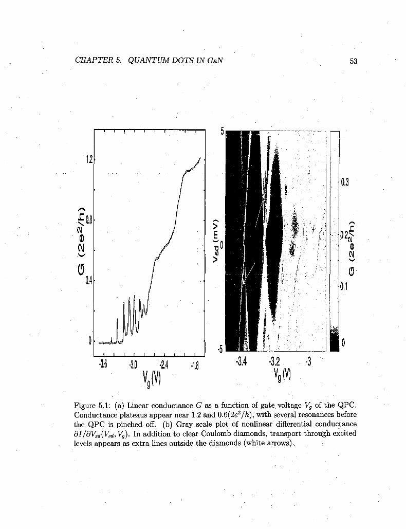
CHAPTER 5. QUANTUM DOTS IN GaN 53
0 2 ^ (D (\l
0 0.1
Figure 5.1: (a) Linear conductance G as a function of gate voltage Vg of the QPC. Conductance plateaus appear near 1.2 and 0.6(2e2//i), with several resonances before the QPC is pinched off. (b) Gray scale plot of nonlinear differential conductance dI/dVsd(ysd, Vg). In addition to clear Coulomb diamonds, transport through excited levels appears as extra lines outside the diamonds (white arrows).

CHAPTER 5. QUANTUM DOTS IN GaN 54
5.2 Accidental quantum dot in quantum point con
tacts
We have fabricated several quantum point contacts (QPCs) with different geometric
design, besides the QPCs reported in previous chapter, in most QPCs the conduc
tance plateaus are not quantized in units of 2e2/h. Figure 5.1(a) shows the linear
conductance as a function of gate voltage for one QPC with profound conductance
feature other than quantized conductance plateaus. The conductance plateaus are
not quantized in multiple of 2e2/h. The deterioration of conductance quantization
in these QPCs might be caused by impurities nearby, or by the nonadiabaticity of
the potential produced by the split gates. When these QPCs are nearly pinched off,
multiple oscillations in conductance are observed, reminiscent of Coulomb oscillations
in a single-electron transistor. Below we show data from one of these QPCs. Similar
behavior has previously been observed in QPCs based on both Si and GaAs, though
it is rarely published (see for example [46]).
Nonlinear transport measurements can be used to extract the charging energy and
the spectrum of excited states of the accidentally-formed quantum dot. To confirm
the origin of the conductance oscillations, we measure the nonlinear conductance as
a function of source-drain bias.and gate voltage (Figure 5.1(b)). The resulting clear
Coulomb diamonds are characteristic of a single-electron transistor. The charging
energy Ec = e2/C is larger for the diamonds at more negative voltage, reaching
7.5 meV for the last diamond, corresponding to a total capacitance C = 21 aF.
Modeling the dot as a disk embedded in GaN and ignoring nearby electrodes, the
capacitance has the form C = 8ereor where r is the disk radius and er = 9 is the
approximate dielectric constant of GaN, and of the AlGaN and AlOx which separate
the 2DEG from the surface gates. From this we estimate the radius of the quantum
dot to be 30 nm and the number of electrons in the dot to be 12 or fewer. Excited
energy levels with a spacing of about 1 meV (indicated by arrows in Figure 5.1(b))
reasonably match the single particle level spacing expected for a 30 nm GaN dot,
A = 2h2/m*r2 = 1 meV, where m* is the effective electron mass.

CHAPTER 5. QUANTUM DOTS IN GaN 55
0.07
csj^ 0.03 -
Figure 5.2: Linear conductance G versus the gate voltage VG3 of the SET. Clear Coulomb Oscillations are observed. Inset (a): Electron micrograph of the SET. The coupling between the 2D reservoirs and the quantum dot can be tuned by controlling the voltages on gates Gl, G2, and G4. By varying the yoltage on the plunger gate G3, the potential of the quantum dot is modified and the energy for adding an electron to the quantum dot is shifted into and out of resonance with; the Fermi level of the 2D reservoirs. A peak in conductance occurs when the addition energy is aligned to the Fermi level so that an electron can tunnel onto and off of the quantum dot. All the data shown in this section are measured by varying the plunger gate G3, with gates G1,G2, and G4 fixed at constant voltages. Inset; (b): A conductance peak fit to the lineshape expected in the classical Coulomb Blockade regime (multi-level transport) - G = G'max cosh-2[a(VG3 - Vmax)/2.5kBT], where Gmax is the peak conductance, a is the conversion ratio from gate voltage to energy, and V ^ is the location in gate voltage of the conductance peak. The three fit parameters are Gmax, Vmax, and v = kBT/a.
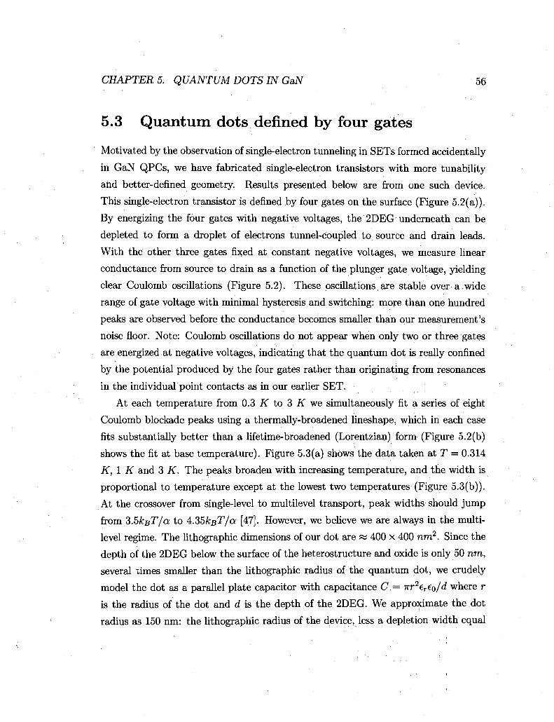
CHAPTER 5. QUANTUM DOTS IN GaN 56
5.3 Quantum dots defined by four gates
Motivated by the observation of single-electron tunneling in SETs formed accidentally
in GaN QPCs, we have fabricated single-electron transistors with more tunability
and better-defined geometry. Results presented below are from one such device.
This single-electron transistor is defined by four gates on the surface (Figure 5.2(a)).
By energizing the four gates with negative voltages, the 2DEG underneath can be
depleted to form a droplet of electrons tunnel-coupled to source and drain leads.
With the other three gates fixed at constant negative voltages, we measure linear
conductance from source to drain as a function of the plunger gate voltage, yielding
clear Coulomb oscillations (Figure 5.2). These oscillations are stable over a wide
range of gate voltage with minimal hysteresis and switching: more than one hundred
peaks are observed before the conductance becomes smaller than our measurement's
noise floor. Note: Coulomb oscillations do not appear when only two or three gates
are energized at negative voltages, indicating that the quantum dot is really confined
by the potential produced by the four gates rather than originating from resonances
in the individual point contacts as in our earlier SET.
At each temperature from 0.3 K to 3 K we simultaneously fit a series of eight
Coulomb blockade peaks using a thermally-broadened lineshape, which in each case
fits substantially better than a lifetime-broadened (Lorentzian) form (Figure 5.2(b)
shows the fit at base temperature). Figure 5.3(a) shows the data taken at T = 0.314
K, 1 K and 3 K. The peaks broaden with increasing temperature, and the width is
proportional to temperature except at the lowest two temperatures (Figure 5.3(b)).
At the crossover from single-level to multilevel transport, peak widths should jump
from Z.hkBT/a to A.35ksT/a [47]. However, we believe we are always in the multi
level regime. The lithographic dimensions of our dot are « 400 x 400 nm2. Since the
depth of the 2DEG below the surface of the heterostructure and oxide is only 50 nm,
several times smaller than the lithographic radius of the quantum dot, we crudely
model the dot as a parallel plate capacitor with capacitance C = 7rr2ere0/d where r
is the radius of the dot and d is the depth of the 2DEG. We approximate the dot
radius as 150 nm: the lithographic radius of the device, less a depletion width equal

CHAPTER 5. QUANTUM DOTS IN GaN 57
-2.38 -2.36 -2.34 -2.32 -2.3 Vg(V)
Figure 5.3: (a) Coulomb Oscillations at three different temperatures. From bottom to top: 0.314 K, 1 K, and 3 K. (b) The fitting parameter 77 = kBT/a as a function of temperature. The line is the least squares fit to the data excluding the two lowest temperature points. The slope is equal to ks/a, yielding an estimate a = 59 meV/Vg.
CHAPTERS. QUANTUM DOTS IN GaN 58
"v/,° -2.35 -2.33 -2.31 -2.29
VgOO
0.2
CM CI) CM "s^*
CJ 0.1
>
P0.82 S ^ /
0) c 0 CO S-0.76
0.7
r r 1 i r —
.lb)' .A
• \
,*"* - ' < %
i i • • • ' ' i
• i
r 9
/
• •
•
1 2 3 4 5 6 7
Figure 5.4: (a) Differential conductance dI/dVSd as a function of plunger gate voltage Vg and source-drain bias Vad- Stable and uniform Coulomb diamonds are observed, (b) Energy spacing between successive adjacent peaks. The average spacing is 0.85 meV with a fluctuation of tens of \xeV
to the depth of the 2DEG. This predicts a charging energy Ec « 0.85 meV and a
single particle level spacing A « 18 \ieV.
Over the range from base temperature T « 0.3 K to T = 3 K, Ec » ksT =
25-250 neV > A, so multiple levels should participate in transport except possibly
at the lowest 1-2 temperature (see below). The slope of the linear variation of peak
width versus temperature yields a = 59 meV/Vg, with nearly zero offset. The sat
uration of width for the two lowest temperature points suggests that the electron
temperature is 0.450 # even when the 3He bath is cooled to 0.3 if. This is surprising
but not shocking, given that we had not at the time installed explicit low-temperature
electrical filters on the 3He cryostat.
CHAPTER 5. QUANTUM DOTS IN GaN 59
To further investigate properties of the SET such as charging energy and ex
cited energy level spacings, we have measured nonlinear transport [Figure 5.4(a)].
The resulting Coulomb diamonds all have a similar size with a charging energy of
~ 0.85 meV, and show minimal switching events over the six hours of measurement.
No clear features of excited levels appear parallel to the boundaries of the Coulomb
diamonds, supporting our contention that the quantum dot is in the multi-level trans
port regime. To better estimate the energy spacing between consecutive electron
additions, we fit each Coulomb blockade peak and take the difference AV̂ , between
successive peak positions derived from our fits. To convert AV^ into an energy spacing
we simply multiply by a extracted from Figure 5.3(b). The gaps between successive
peaks are all about 0.85 meV, providing a more precise measurement of charging
energy (Figure 5.4(b)). The agreement with our prediction is gratifying, though the
precise match is certainly fortuitous. The charging energy has an overall trend of
increasing slightly with more negative gate voltage - larger indices in Figure 5.4(b)
represent peaks at more negative voltage. This is due to a gradual reduction of the
dot size. We have performed nonlinear transport around a more negative voltage
Vg = —4.2 V, and found a charging energy of lAmeV from Coulomb diamonds, con
firming this trend. On top of the smooth increase in charging energy, the fluctuations
in peak spacings are of the same order as the estimated single energy level spacing
~30/xeV.
In conclusion, we have fabricated QPCs on a GaN/AlGaN heterostructure and
studied an accidental quantum dot formed in a QPC. An intentionally-fabricated
SET on a GaN/AlGaN heterostructure showed more than a hundred of consecutive
Coulomb oscillations. This SET is in the multi-level transport regime where no excited
level spectrum is visible in the Coulomb diamonds. In order to resolve the excited level
spectrum, explore interesting phenomena such as Kondo effect and and investigate
how the strong electron-electron interactions affect peak-spacing statistics, it requires
to measure this SET at a temperature lower than 0.1 K : A = 18 fieV > ksT =
8.6 fieV at 100 mK to achieve single-level transport, or to fabricate new quantum
dots with reduced lateral dimensions. In the next chapter the peak-spacing statistics
measurement on a GaN quantum dot in a dilution fridge with a 100 mK electron

CHAPTER 5. QUANTUM DOTS IN GaN 60
temperature will be presented.
Chapter 6
Statistics of CB Peak Spacings in
GaN Quantum dots
The spectra of many chaotic quantum systems do not have analytical solutions but
rather exhibit random fluctuations with universal statistical features. Although it is
difficult to describe the detailed physical properties of a chaotic system, what can
be well described is the ensemble statistics of the physical properties, which follows
the underlying symmetry of the Hamiltonian and does not depend oh the specific
system being studied. Universal statistical behaviors have been observed in many
different complex quantum systems that have the same space-time symmetry and are
described remarkably well by Random Matrix theory (RMT) [48]. Some experimen
tal examples are neutron resonances of nuclei, energy spectra of hydrogen atom at
high magnetic field and the eigenmodes of billiard shaped microwave cavities[15]. In
recent years, semiconductor quantum dots has emerged as an alternative candidate
to check the predictions of RMT. Due to the random potential profile produced by
the irregular device boundary or impurity configuration, the spectrum and electronic
wave functions in most many-electron quantum dots are assumed to be chaotic and
have been studied theoretically in the framework of RMT': In a non-interacting pic
ture, RMT has been successful in predicting fluctuation of conductance in open dots
system. For closed dot systems, RMT has also been successfully applied to describe
the distributions of Coulomb Blockade peak heights[15].
61
CHAPTER 6. STATISTICS OF CB PEAK SPACINGS IN GaN QUANTUMDOTS62
Nonetheless, the prediction on the distribution of CB peak spacings made by RMT
for a spin-degenerate quantum dot, the famous bimodal Wigner surmise distribution
with a standard deviation proportional to the average energy level spacing, has not
been observed clearly in any of the quantum dot experiments. Instead, Gaussian-like
distributions of CB peak spacings have been observed in many experiments with the
standard deviation varying widely among different experiments[49, 50, 51, 52, 53].
The contrast between RMT predictions and experimental results, and also the incon
sistency between different experimental observations have attracted much theoretical
effort[54, 55, 56, 57, 58, 59, 60, 61, 62, 63], where many different effects such as
electron-electron interaction or finite temperature have been taken into account.
In this chapter we present our measurement on the distributions of CB peak spac
ings in GaN quantum dots, where the ratio of electron-electron interaction to kinetic
energy is stronger than all the previous quantum dots that have been studied for
distributions of CB peak spacings. A brief introduction to RMT predictions on dis
tributions of CB peak spacing, the bimodal Wigner surmise distribution, and previous
experimental results will be provided, followed by our characterization method and
experimental results on GaN quantum dots.
6.1 Distributions of Coulomb Blockade Peak Spac
ings: Theory
Random Matrix Theory predicts the distribution of energy level spacings of spin-
degenerate quantum dots with time-reversal symmetry (or any other chaotic quan
tum objects that has the same symmetry) to have the form of Gaussian Orthogonal
Ensembles (GOE),
PGOE(S) = \seSs2 (6.1)
where s is in units of the average spin-degenerate energy level spacing, A = ^ j , as
introduced earlier in chapter 2. If time-reversal symmetry is broken with a small per
pendicular magnetic field, the distribution is predicted to have the form of Gaussian

CHAPTER 6. STATISTICS OF CB PEAK SPACINGS IN GaN QUANTUMD0TS6S
Unitary Ensembles (GUE).
32 PGUE{S) = -^s2e~~ (6.2)
To probe the energy level spacing distribution, one can relate the energy level
spacing with the CB peak spacing by using equation 2.6, reproduces here for conve
nience:
U = Ec + &N,N+1 = e2jC + sN+l - eN = nAVg (6.3)
Here for simplification we neglect exchange interaction and we further assume that
the quantum dot is spin-degenerate. When N is an odd number, the N+ls t electron
fills the same degenerate level with an opposite spin as the Nth electron, which means
£JV+I = SN in equation 6.3, therefore the addition energy is simply the charging energy
Ec.
U = EC = rjAVg N : odd number •;•; • .. • (6.4)
On the other hand, when N is an even number, each level is filled with a pair of
electrons with opposite spins. The N+ls t electron has to fill a different energy level
from the Nth electron, so that the addition energy is the combination of the charging
energy Ec and the energy level spacing A ^ J V + I •
U = Ec + AJV,;V+I = V^Vg N : even number (6.5)
Assuming both the gate-energy conversion n and charging energy Ec remain nearly
constant with respect to gate voltage, one would expect the appearance of spin pair
ing in CB measurement as shown in Fig 6.1(c). The CB peaks should appear in pairs
which each pair has a constant and smaller intra-pair distance (~ Ec) in gate volt
age compared to the distance (~ Ec + A) between adjacent peaks belonging to two
different pairs. By converting the spacing into energy and subtracting off a constant
charging energy Ec, this predicted distribution of CB peak spacing may be related to
the distribution of level spacings of quantum dots and has a bimodal distribution,
P(8) = 1(6(8)+ ^8eS*) B = 0 (6.6)

CHAPTER 6. STATISTICS OF CB PEAK SPACINGS IN GaN Q UANTUM DOTS64
(a)
Source
(b)
Source
N- •N+1
Ec+A
f-t" t"+ 1-t
N+1-+N+2
4 t-t -r-t-1-t-
(c)
Drain
o
iS "o = >
• o tz o O
Drain
~EC
•*—H
Gate voltage
Figure 6.1: (a) Energy diagram of a quantum dot filled with N electrons where N is an even number. All the filled levels are occupied by pairs of electrons, with opposite spins. Besides the charging energy, the next N+Ist electron has to pay an extra energy because of the requirement of filling to a different quantum state, so the distance to next allowed level is Ec + A. (b)Similar to (a) with a change in gate voltage such that the dot is filled with N electrons. The highest occupied level is only filled with the unpaired N + lst electron. So the N + 2th electron can enter the dot via the same quantum state so the distance to the next level is simply Ec-t (c)A cartoon of Coulomb Blockade peaks versus gate voltage. The CB peaks appear in pairs that has an intra-pair distance proportional to Ec, and a larger distance proportional to Ec + A between the adjacent peaks that belong to different pairs. Note that here level spacing is taken to be constant = A, whereas in fact it should be different for different levels

CHAPTER 6. STATISTICS OF CB PEAK SPACINGS INGaN QUANTUM DOTS65
Figure 6.2: (a)Plot of equation 6.6 where magnetic field is zero. (b)P16t of equation 6.7 where the time reversal symmetry is broken when magnetic field is not zero.
P(a) = h6(8) + ^e-^) 5^0 (6.7)
where in both equations s is again in units of the average spin-degenerate en
ergy level spacing. As shown in Figure 6.2, each distribution consists of a sharp
delta-function distribution corresponding to the charging energy and another broader
distribution that represents the distribution of the level spacings predicted by RMT.
Including the ^-distribution, the CB peak spacings for 5 = 0 have a broader dis
tribution (standard deviation: o = 0.62A) than the CB peak spacing for B ^ 0
(o- = 0.58A, a(B = 0)/cr(B ^ 0) = 0.62A/0.58A:w 1.1).
The predicted bimodal distribution is caused by spin degeneracy. If the spin
degeneracy is lifted, since the whole ensembles can be divided into two indepen
dent random-matrix ensembles representing spin up and spin down subspace, the CB
peak spacings distribution can be derived from two overlapping Wignef-Dyson dis
tributions. This is called spin-resolved RMT and the resulting distribution is still
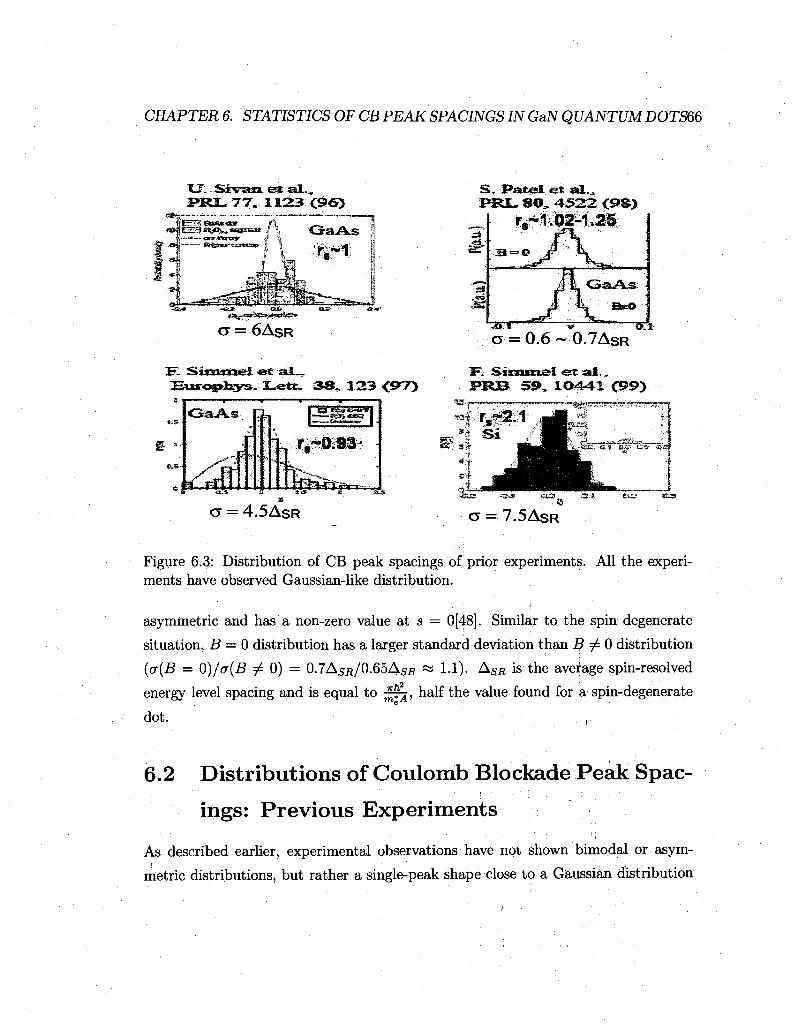
CHAPTER 6. STATISTICS OF CB PEAK SPACINGS IN GaN QUANTUM DOTSffi
PJtZ. 77. . 1123: <9<S)
a = 6 A S R
Ewroipabcys,:. JLett . » 8 « 1 2 3 <©7>
G a A s
kyQ sac **&
CT = 4 . 5 A S R
S . I>attsel e t a l „ P R L SO, 4 5 2 2 <9S>
r_~1.02-1.25
•an——"—-^r———&\ CT = 0.6 ~ 0 . 7 A S R
3F; SisxLttxel est a l . , f»j&B, SB** 1044 -1 <9>S>>
CT = 7 . 5 A S R
Figure 6.3: Distribution of CB peak spacings of prior experiments. All the experiments have observed Gaussian-like distribution.
asymmetric and has a non-zero value at 5 = 0[48].' Similar to the spin degenerate
situation, 5 = 0 distribution has a larger standard deviation than B ^ 0 distribution
(cr(B = 0)/(T(B ^ 0) = 0.7ASR/0.65ASR « 1.1). A5fl is the average spin-resolved
energy level spacing and is equal to ^ ^ , half the value found for a spin-degenerate
dot . ' • • . - . ' , ;
6.2 Distributions of Coulomb Blockade Peak Spac
ings: Previous Experiments
As described earlier, experimental observations have not shown bimodal or asym
metric distributions, but rather a single-peak shape close to a Gaussian distribution
CHAPTER 6. STATISTICS OF CB PEAK SPACINGS IN GaN QUANTUM DOTS67
[Figure 6.3]. Since no bimodal distribution is observed, researchers have naturally as
sumed spin degeneracy in quantum dots is lifted and have compared the experimental
results with the spin-resolved RMT. The first experiment on this topic was done in
a GaAs dot with a rs of 1 by Sivan et al. in 1996[49]. A single Gaussian distribution
was observed with a standard deviation (a ~ 6A.SR ~ Q.1EC), an order larger than the
prediction by spin-resolved RMT. Simmel et al. have done measurements in a GaAs
dot with a smaller rs and still observed an enhanced cr[50]. They also measured a Si
quantum dot with a larger rs of 2.1 and observed an enhanced a[51]. On the other
hand, Patel et al. measured seven GaAs quantum dots with rs ~ l[52j. Although
they also observed a single Gaussian distribution in all the quantum dots, both a
and also the ratio of a(B = 0)/(T(B =£ 0) were close to the value predicted by RMT
in the spin-resolved regime. In another GaAs quantum dot measurement done by
Liischer et al. with a smaller rs of 0.7, a a comparable to A was observed. It also
showed spin-pairing effects in the parametric dependence of the peaks where a pair
correlation vs. magnetic field in peak amplitude and position is observed[53].
The observation of a single Gaussian distribution with an enhanced a in some
experiments has triggered many theoretical works, and electron-electron interaction
has been one possible explanation for the enhanced a. For example, by including
electron-electron interaction in their numerical simulation of the ground state level
statistics of interacting electrons on a small 2D disk, Sivan et al. found a good
agreement between the observed standard deviation and their simulation results. In
their simulation when the dimension-less interaction strength rs is larger than 0.75,
the fluctuation of the peak spacing depends more on the fluctuation of the charging
energy from one added electron to the next than the fluctuations of level spacings.
The simulated distribution agrees with their experiment results better than RMT
does[49]. Other works including self-consistent Hartree-Fock or exact diagonalization
have also shown a similar trend: a stronger rs results in a greater <r[54, 55]. Although
these numerical calculations can only be done in a quantum dot with a small number
of electrons, they account for the Gaussian shape of the distributions and the larger-
than-expected width. On the other hand, theoretical works treating the exchange
interaction as a weak perturbation yield a decreasing o with an increasing exchange

CHAPTER 6. STATISTICS OF CB PEAK SPACINGS IN GaN QUANTUM DOTS68
interaction [56, 57, 58]. Readers who want to know more about the theoretical work
may refer to the review articles by Alhassid or Aleiner[15, 16] and the references
therein.
With these different experimental observations and theory predictions, one might
expect to further examine how electron-electron interaction affects the distribution
by going to a higher rs. In the following sections our measurement results on a GaN
quantum dot with a stronger rs will be presented.
6.3 Experimental Results in GaN Quantum Dots
6.3.1 Device Characterization
The GaN quantum dot used in this experiment is the same as the one in chapter 5,
where the reader can find more detailed information for the 2DEG properties and
device geometry. The dot has a lithographic size of 200 nm in radius. Assuming a
lateral depletion of 50 nm(2DEG depth + the Alumina layer thickness), the radius of
the dot is 150 nm, and the spin-resolved single particle level spacing A$R is derived
to be « 18 fieV. The dot has a r , of 2.7 assuming the dot has; the same density as
the 2DEG. In order to fulfill the requirement of single level transport (A ;» /csT),
the experiment is performed in a dilution refrigerator with a base temperature of 12
mK, using standard ac lock-in techniques, with a 2/iV, 77 Hz excitation added to a
variable dc voltage Vad. As shown in Figure 6.4, clear Coulomb oscillations over a wide
range of gate voltage and also Coulomb diamonds with charging energy « 0.84 meV
are observed. The CB peaks are much narrower compared to the data in chapter
5, reflecting a lower electron temperature. To have a more precise estimation of the
effective electron temperature, the quantum dot is measured at a series of different
temperatures. We then fit a series of CB peaks using a thermally-broadened lineshape,
which in each case fits substantially better than a lifetime-broadened (Lorentzian)
form (Figure 6.5(a) inset shows the fit at base temperature). The peaks broaden with
increasing temperature, and the width is proportional to temperature except at the
lowest three temperatures (Figure 6.5(a)). As shown in Figure 6.5(b), the observation

CHAPTER 6. STATISTICS OF CB PEAK SPACINGS IN GaN QUANTUM DOTS69
0 . 2 0
o ; i 5 —i
CM
O o. io
o.os —i
o.oo
( a )
iw^rfrllfiliVi ,.-..,..4. JLJL - r . . T - j - . ,... . — — p -.rj;-.•;-•..-,---. ""FT
-21 Op -2QQP -1SPP -iepp -ITPO --I6PP ^rSPP
( b )
3 0 0 -
2 0 0 -
1 0 0 -
0 -
- 1 0 O
-209 -
-300-
Vg (mV) . •
^^^^^^H^^^^^^H
^^^^^^S^^^^SS^^^^^^^^^^^
-180 0 -17 80 -17 60 -17 40 -172 0
Vg (mV)
Figure 6.4: (a)Linear conductance G versus plunger gate voltage of the quantum dot. Clear Coulomb Oscillations over a wide range of voltage were observed. (b)Differential conductance dI/dVsd as a function of plunger gate voltage Vg and source-drain bias Vsd- The charging energy is « 0.86 meV estimated from the Coulomb Diamond

CHAPTER 6. STATISTICS OF CB PEAK SPACINGS IN GaN QUANTUMDOTS70
of peak height inversely proportional to temperature indicates that electron transport
is indeed only via a single level (see Equation 2.5). The saturation of width and also
the height for the three lowest temperature points suggests that the lowest electron
temperature is 100 mK, even when the base temperature of the fridge is « 10 mK.
The broader width might due to noise heating but in this same dilution fridge with
a same electronic measurement setup, base electron temperature of 12 ~ 13mK has
been consistently achieved for GaAs quantum dots with a rs ~ 1. It also has been
suggested that in a strongly-interacting quantum dot, the peak width does not vanish
when temperature approaches zero[64]. Another important factor to consider is in this
quantum dot, the plunger gate has a leakage current of 0.5 nA when the gate voltage
is —2 V. Assuming the heat is all flowing into the 2DEG and the heat conduction is
mainly via the 2DEG, this 1 nW power input could easily heat the 2DEG locally to
100m.&:(AppendixB).
6.3.2 Distributions of CB peak spacings ensemibles
Figure 6.6(a) shows typical CB peak data measured at zero magnetic field. To extract
the CB peak spacings, each CB peak is fitted with a thermally-broadened lineshape
to find the peak position in gate voltage. The average peak spacings increase with
more negative gate voltage, reflecting a decreasing capacitance of the dot to the
gate[Figure 6.6(b)]. To account for this dot capacitance change, a funning average
spacing < AV > is estimated by fitting the spacing AV to a linear function of gate
voltage. This < AV > is then used to calculate the normalized spacing for each
pair of peak: 5=(AV- < AV >)/ < AV > [Figure 6.6(c)]. By stepping voltage on
another gate, sweeping the plunger gate voltage and repeat the procedure mentioned
above, multiple sets of CB peaks are measured and more than seven hundred CB peak
spacings at B=0 are collected. To break the time-reversal symmetry, a magnetic field
at +50 mT or -50 mT is applied and nearly three hundreds of CB peaks are collected.
Estimated from the correlation of the peak height and peak spacing[65], the required
gate voltage to scramble the quantum dot spectrum is about twice the step size of the
voltage on another gate, therefore about half of the data is assumed to be; statistically
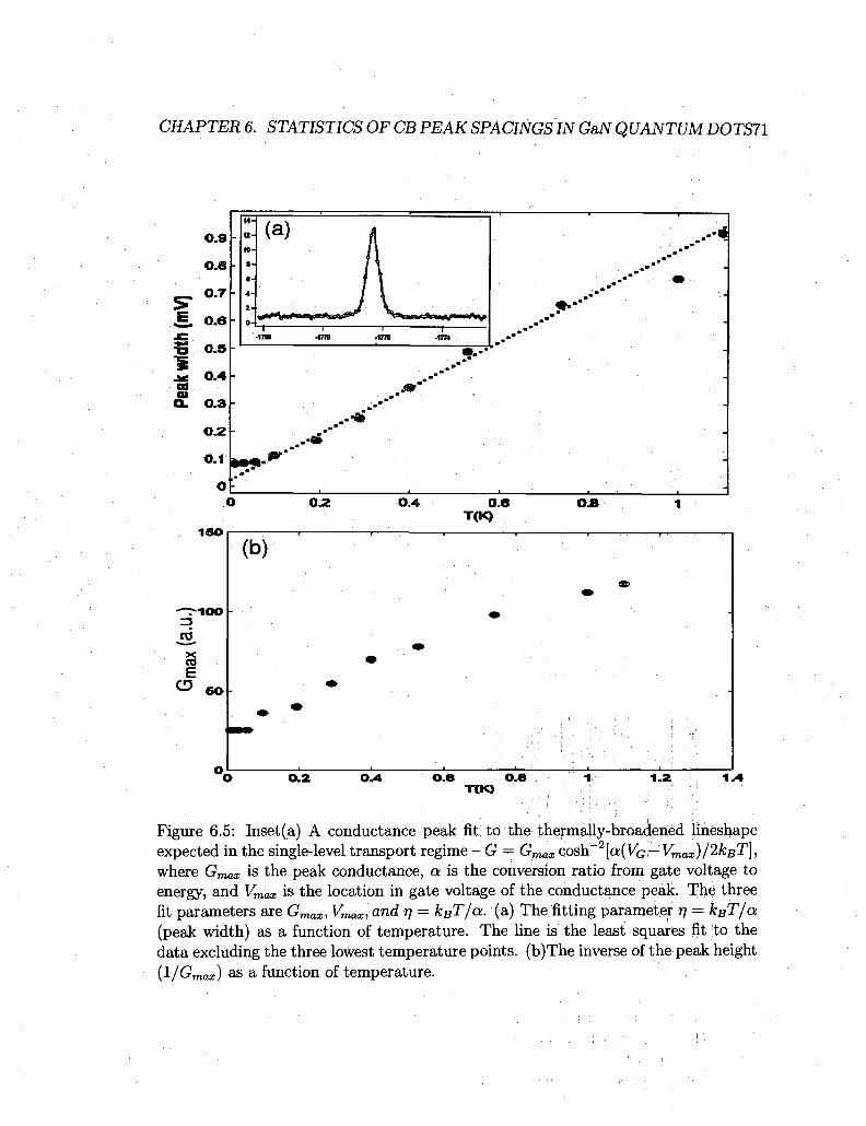
CHAPTER 6. STATISTICS OF CB PEAKSPACINGSIN GaN QUANTUMD0TS71
Figure 6.5: Inset(a) A conductance peak fit to the thermally-broadened lineshape expected in the single-level transport regime -G = Gmaicosh_2[a(VG:— Vrrlax)/2kBT], where Gmax is the peak conductance, a is the conversion ratio from gate voltage to energy, and Vmax is the location in gate voltage of the conductance peak. The three fit parameters are Gmax, Vmax,and 77 = ksT/a. (a) The fitting parameter 77 = ksT/a (peak width) as a function of temperature. The line is the least squares fit to the data excluding the three lowest temperature points. (b)The inverse of the peak height (l/Gmax) as a function of temperature.
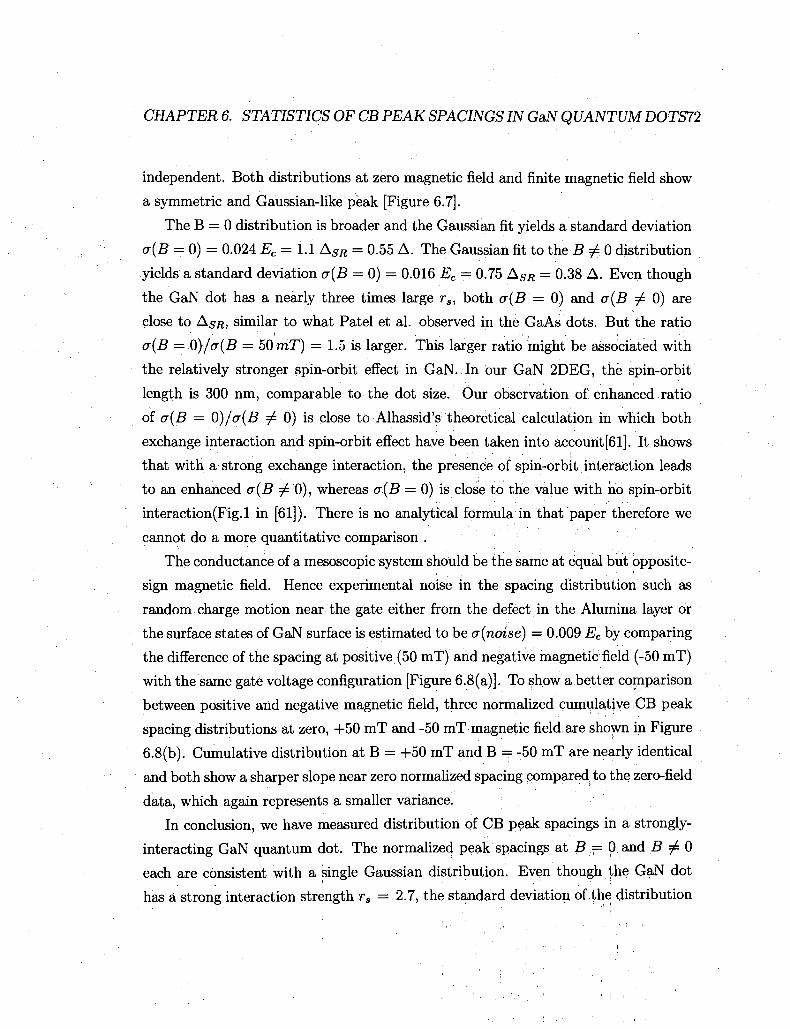
CHAPTER 6. STATISTICS OF CB PEAK SPACINGS IN GaN QUANTUM DOTS72
independent. Both distributions at zero magnetic field and finite magnetic field show
a symmetric and Gaussian-like peak [Figure 6.7].
The B = 0 distribution is broader and the Gaussian fit yields a standard deviation
a(B = 0) = 0.024 Ec = 1.1 ASR = 0.55 A. The Gaussian fit to the B f.. 0 distribution
yields a standard deviation o(B — 0) = 0.016 Ec = 0.75 ASR = 0.38 A. Even though
the GaN dot has a nearly three times large rs, both cr(B = 0) and cr(B ^ 0) are
close to ASR, similar to what Patel et al. observed in the GaAs dots. But the ratio
a(B = Q)/a(B = 50 mT) = 1.5 is larger. This larger ratio might be associated with
the relatively stronger spin-orbit effect in GaN. In bur GaN 2DEG, the spin-orbit
length is 300 nm, comparable to the dot size. Our observation of enhanced ratio
of a(B = 0)/a(B ^ 0) is close to Alhassid's theoretical calculation in which both
exchange interaction and spin-orbit effect have been taken into account[61]. It shows
that with a strong exchange interaction, the presence of spin-orbit interaction leads
to an enhanced a{B ^ 0), whereas a{B = 0) is close to the value with no spin-orbit
interaction (Fig. 1 in [61]). There is no analytical formula in that paper therefore we
cannot do a more quantitative comparison .
The conductance of a mesoscopic system should be the same at equal but opposite-
sign magnetic field. Hence experimental noise in the spacing distribution such as
random charge motion near the gate either from the defect in the Alumina layer or
the surface states of GaN surface is estimated to be a(noise) = 0.009 Ec by comparing
the difference of the spacing at positive (50 mT) and negative hiagnetic field (-50 mT)
with the same gate voltage configuration [Figure 6.8(a)]. To show a better comparison
between positive arid negative magnetic field, three normalized cumulative ;CB peak
spacing distributions at zero, +50 mT and -50 mT magnetic field are shown in Figure
6.8(b). Cumulative distribution at B = +50 mT and B = -50 mT are nearly identical
and both show a sharper slope near zero normalized spacing compared to the zero-field
data, which again represents a smaller variance.
In conclusion, we have measured distribution of CB peak spacings in a strongly-
interacting GaN quantum dot. The normalized peak spacings at B = 0 and B ^ 0
each are consistent with a single Gaussian distribution. Even though the GaN dot
has a strong interaction strength rs = 2.7, the standard deviation of the distribution
CHAPTER 6. STATISTICS OF CB PEAK SPACINGS INGaN QUANTUM D0TS7Z
0.35
0 3
0.25
0 2
tO t3
0.15 o O
0.1
0.05
! t t T T I T i l l T.. . . . . . t T T U L J L A J L u LU -2300 -2200 -2100 -2000 -1900
gate voltage (mV) 0.08
1800 -1700 -1600
CO o
Q_ -2300 -2200 -2100 - 2 0 0 0 - 1 9 0 0 - 1 8 0 0 - 1 7 0 0 -1600
gate voltage (mV) spacing index
Figure 6.6: (a)Coulomb Blockade peak data over a wide range of gate voltage. Each peak is fitted with a thermally-broadened lineshape and the red dot represents the peak position and height. (b)From the fitting in (a), spacing between consecutive peaks is calculated and plotted as a function of gate voltage. To take into account the change of the dot capacitance as gate voltage is varied, the running spacing average is estimated by a linear fit (black line) to the spacing data. (c)Normalized spacing after subtracting the running average spacing: 5=(AV— < AV >)/ < AV >.

CHAPTER 6. STATISTICS OF CB PEAK SPACINGS IN GaN QUANTUM DOTS!A
30
20
10
O
-a.
90
so
70
eo <f> S O
o ""> o 30
20
10
o -o.
0.0s 0 .1
. ( b )
-
-
-
-
— 1
/ i 1 1
/ 1 ' 1 t 1
/ 1 ' • 1 ' H I
VH H 1 / • • 1 / • •
• \ I * I *
I H* 1 i i • • \
I H mt\ I 1 1 v
, . , . - — ,.r„,,.———,— —,,. „
B = SOmT '
,~
' ; . - . -
•
' ! ;' . . • • . .
l_
-O.OS O.OS 0 . 1
S p a c i n g ( E c )
Figure 6.7: (a)CB peak spacing distribution at zero magnetic; field. The distribution is Gaussian-like and the standard deviation is a(B = 0) = 0.024 Ec = 1.1 ASR (b)CB peak spacing distribution at B = 50 mT. The distribution is also Gaussian-like but has a smaller standard deviation a(B = 0) = 0.016 Ec — 0.75 ASR

CHAPTER 6. STATISTICS OF CB PEAK SPACINGS IN GaN QUANTUM DOTS75
0.03
0.02 CM
o 0.01
(a)
-2040
-50 mT • +50 mT
_[ [•rwr- miMiTiii i i • iinmimni m MriUinftini H » HH«H u w t j B&*<***J% 1/m*&a&0mj*if WM^WWIMUW
-2020 -2000 -1980 Gate Voltage (mV)
-1960
- 5 O 5 x
n o r m a l i z e d p e a k s p a c i n g (A S R ) 1 0
Figure 6.8: (a)CB peak data at B = +50 mT and B = -50 mT. Experimental noise is estimated to be the standard deviation of the spacing difference 8(noise) = S(+50mT) - £(-50 mT): <r(8{noise)) = 0.009 Ec (b)Cumulative distribution of CB peak spacings in +50 mT, —50 mT and zero magnetic field.

CHAPTER 6. STATISTICS OF CB PEAK SPACINGS IN GaN QUANTUM DOTS76
of the CB peak spacing is close to mean level spacing, comparable to the results of
Patel's and Liischer's measurements at a lower rs[52, 53]. The ratio between a(B = 0)
and <x(B ^ 0) is 1.5 which is larger than the prediction by RMT and might due to
the spin-orbit interaction. In order to confirm this, future work such as temperature
and density-dependent experiments will be essential and very interesting.

Appendix A
Fabrication Details
In this appendix the details of device fabrications are presented. In the heterostruc-
ture we use, a 700 nm to 1 /xm thick GaN layer followed by a 20 nm thick AlGaN
layer is grown on a GaN/Sapphire template by molecule beam epitaxy (MBE) by
our collaborator Michael Manfra at Bell Laboratories (now at Purdue University).
The growth of the 2 inch GaN/Sapphire template is done by growing a very thick
GaN layer (15 to 20 fj,m) on the Sapphire substrate by hydride vapdr phase epitaxy
(HVPE) by Dr. Richard Molnar at Lincoln Laboratories.
A.l Cutting and Cleaning
After receiving the 2-inches wafer from Bell Laboratories, the wafer is sent to a dicing
company to cut the sample into squares with a 5 mm size. The dicing company is
Micro Dicing Technology and their service is fast, precise and in-expensive, especially
for cutting Si wafer (cutting 3-4 wafers for 150 dollars). The person to contact and
consult for the service is Peter Chiang, 1111 Elko Drive, Bldg H Sunnyvale, CA 94089,
(408) 734-8779. Since the wafer is 2 inches and the substrate is sapphire which is hard
to cut, the technician mounted the wafer on a 6 inches Si wafer by using wax. After
the wafer is cut and sent back to us, the wax is removed by immersing the wafer into
Acetone heated at 60° C. Usually it requires about 30 minutes to an hour of immersion
for removing the wax. After the wax is removeds each 5 mm square sample is washed
77
APPENDIX A. FABRICATION DETAILS 78
in Acetone, then Isopropanol and then DI water.
A.2 Process Recipe
The tweezers I used to handle the sample are carbon fiber tip tweezers, which can be
ordered from www.techni-tool.com. It is made of anti-magnetic, anti-acid stainless
steel and combines the softness of plastic tweezers and the precision of metal tweezers.
1. Clean step: All the rinse steps are done in beakers (lOOmL) with cleaning
solution filled about half of the beaker height. The beakers are placed in the sonicator
for ultrasonic sonication. The sonicator is filled with water and the level of the water.
The level of the water should not be higher than one third of the beaker since otherwise
the beaker might be easily tilted over during cleaning, (a) Immerse in Acetone for
5 minutes, with ultrasound, (b) Immerse in Isopropanol (IPA) for 5 minutes, with
ultrasound, (c) Immerse in DI water, with ultrasound, (d) Blow dry with compressed
Nitrogen gas. (e) Singe on the center of a hotplate at 180°C for 5 minutes.
2. Photolithography step: Photolithography is done by using Karlsuss mask
aligner in the clean room at Ginzton Lab.
(a) After clean step, spin coat photoresist Shipley 1813 at 5000 RPM for 30 seconds
and then bake on the center of a hotplate at 115°C for 90 seconds.
(b) Expose photoresist using Karlsuss mask aligner at Ginzton clean room. Ex
posure time: 3 seconds. Intensity: Unknown, the Mask Aligner doesn't have an
intensity meter with it and the power supply of the lamp is set at constant current
mode. Therefore the exposure time is mainly based on empirical experience. I usually
prepare a dummy sample for testing the exposure time.
(c) Develop in Microchem CD-26 or CD-30 developer for 60 seconds. If Alumina
has been deposited on device surface as a gate dielectric, it is crucial not to use CD-26
developer because Alumina is etched away in CD-26. Rinse in DI water and blow dry
afterwards.
3. Ohmics: Ohmic metal consists of a bilayer of Ti (10 nm)/Al (200 nm) deposited
either by myself using KGB lab's RIBE e-beam evaporator or by Tom Carver at
Ginzton lab using the e-beam evaporator inside Ginzton clean room. Before the

APPENDIX A. FABRICATION DETAILS 79
samples are loaded into the chamber for evaporation, Tom did a Buffered Oxide Etch
(BOE etch) using HF:Water (1:20) for 60 seconds to remove the native oxide, though
ohmics worked also when I did the evaporation myself without doing BOE etch. The
ohmics are annealed in a tube furnace (located in Moore Building, room 089) at
540°C with a constant flow of forming gas (H2/Ar2) ior 15 minutes. Note that the
tube furnace is heated to 540PC first and then samples are placed on a quartz boat
and inserted into the center of the furnace.
4. Etch:
(a) PQUEST plasma etch at SNF. Etch recipe: 5 seem Ar, 10 seem BCl3, 40 seem
Cl2, 500W of ECR power and MOW of RF power, sample chuck heated to 80C. Etch
rate: 80-100 nm/minute.
(b) Argon Mill using RIBE system owned by KGB lab. Follow the procedure
written by KGB lab people which can be found next the the RIBE system in Moore
Building Room 089. Etch rate: 1 nm/minute. The RIBE systems takes a longer time
for pumping down and etching but gives a more uniform etch profile.
5. E-beam lithography: Before our lab bought our own e-beam lithography tool,
the e-beam lithography process was done by using Raith 150 at SNF. The single layer
process gives a better resolution than bilayer process. On the other hand, bilayer
process gives a better liftoff and also the availability of thicker metal evaporation (50
nm compares to 30 nm for single layer process).
Single layer process (for 30 nm resolution):
(a) 2% 950K PMMA in chlorobenzene 5000 rpm for 40 seconds, baked at 180°C
for 15 minutes on a hotplate.
(b) The beam energy is 20KV and the dose is 120fiC/cm2 (higher voltage such
30KV was not allowed at the time I operated Raith 150.).
(c) Develop in MIBK+IPA (1:3) for 60 seconds.
(d) Stop the development in IPA and then blow dry with Nitrogen gas.
Bilayer process (the resolution is about 50 nm):
(a) Bottom layer: Spin 5% 495K PMMA in chlorobenzene at 5000rpm for 60
seconds and bake at 180°C for 15 minutes.
(b) Top Layer: Spin 2% 950K PMMA in chlorobenzene 5000 rpm for 60 seconds,

APPENDIX A. FABRICATION DETAILS 80
bake at 180°C for 15 minutes
(c) The beam energy is wOKV and the dose is 200 fiC/cm2.
.(d) Develop in MIBK+IPA (1:3) for 60 seconds.
(e) Stop the development in IPA and then blow dry with Nitrogen gas.
It is very easy to have charging problem since the substrate is sapphire (insulating).
A 5 nm Cr layer evaporated on top of PMMA can fix the charging problem. After
doing the e-beam exposure and right-before the development, the Cr layer is etched
by dipping into a Cr etch solution for 30 seconds(Chromium Etchants 1020, Transene
Company, Inc.). I later also found without the Cr layer, by just bridging the edge
of the sample surface to the e-beam sample holder using a carbon tape, the charging
problem is highly suppressed too.
In the past three years the e-beam lithography is done by using our lab's e-beam
tool (Philips, XL30 SFEG), a converted SEM with Nabity hardware + software,
shared with Cui and Melosh groups in Material Science departments. A different
bilayer process is used to produce nice undercut for better lift-off and even thicker
metal evaporation (80 nm) compared to the bilayer process stated above.
(a) Bottom layer (MMA (8.5) EL10, a copolymer mixture of PMMA and 8.5%
methacrylic acid, 10% in Ethyl Lactate): Spin 60s at 4000 RPM and bake 5 minutes
at 160°C.
(b) 2nd Layer (2% 950K PMMA in Anisole): Spin 60s at 4000 RPM and bake 5
minutes at 180°C.
(c) The beam energy is 30KV. The dose is 260/xC/cm2.
•(d) Develop in MIBK+IPA (1:3) for 60 seconds.
(e) Stop the development in IPA and then blow dry with Nitrogen gas.
6. Dielectric layer and metal gate deposition: Deposit AI2O3 (SOnm thick) on the
surface of the sample by Cambridge Nanotech Savannah atohiic layer deposition sys
tem in Goldhaber-Gordon lab. The two precursors are Trimethylaluminium (TMA)
and water. The deposition temperature is 100°C. The exact recipe can be found in
the manual. Gate metal is usually 30 to 50 nm Ni deposited by e-beam evaporation
by using the RIBE system myself or done by Tom Carver.
7. Lift off: Immerse the sample in a beaker filled with1 Acetone for an hour or
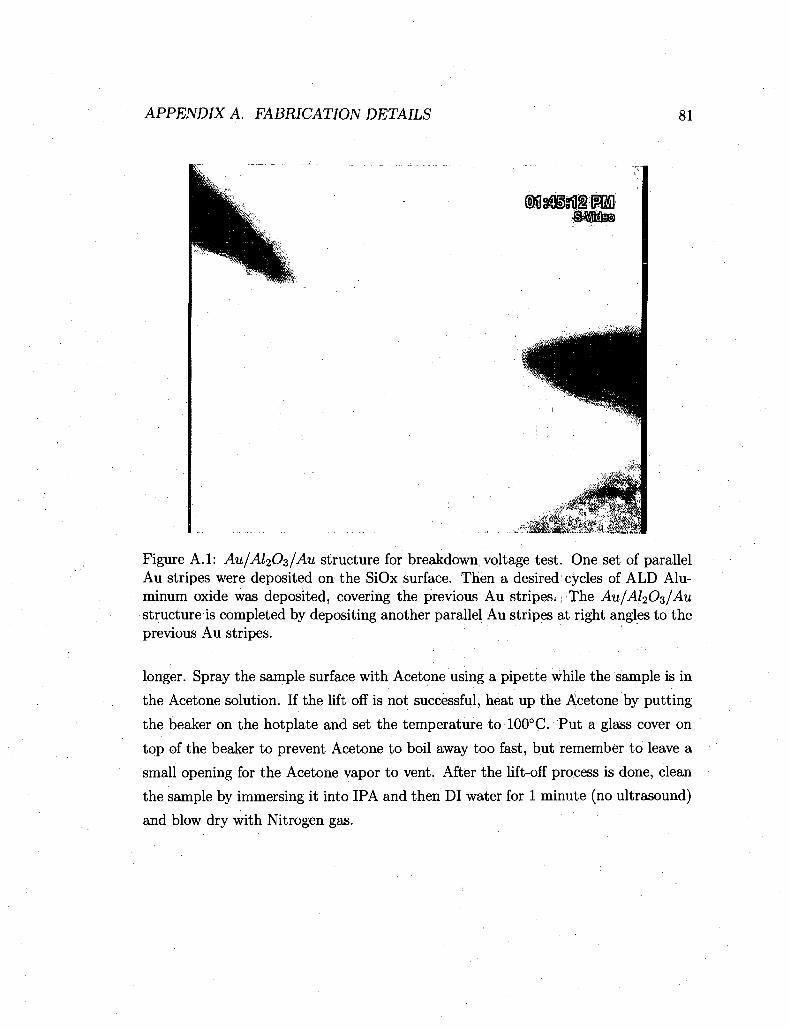
APPENDIX A. FABRICATION DETAILS 81
Figure A.l: Au/A^Oz/Au structure for breakdown voltage test. One set of parallel Au stripes were deposited on the SiOx surface. Then a desired cycles of ALD Aluminum oxide was deposited, covering the previous Au stripes^ The Au/AhO^/Au structure is completed by depositing another parallel Au stripes at right angles to the previous Au stripes.
longer. Spray the sample surface with Acetone using a pipette while the sample is in
the Acetone solution. If the lift off is not successful, heat up the Acetone by putting
the beaker on the hotplate and set the temperature to 100°C. Put a glass cover on
top of the beaker to prevent Acetone to boil away too fast, but remember to leave a
small opening for the Acetone vapor to vent. After the lift-off process is done, clean
the sample by immersing it into IPA and then DI water for 1 minute (no ultrasound)
and blow dry with Nitrogen gas.
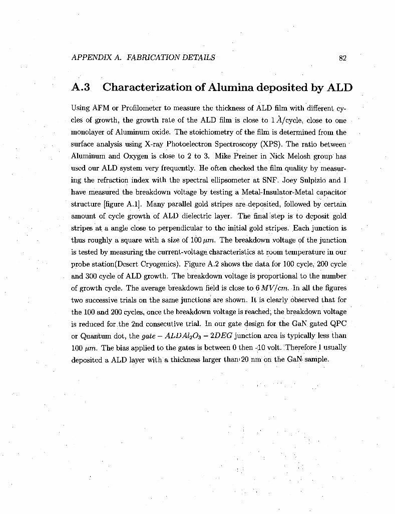
APPENDIX A. FABRICATION DETAILS 82
A.3 Characterization of Alumina deposited by ALD
Using AFM or Profilometer to measure the thickness of ALD film with different cy
cles of growth, the growth rate of the ALD film is close to 1 A/cycle, close to one
monolayer of Aluminum oxide. The stoichiometry of the film is determined from the
surface analysis using X-ray Photoelectron Spectroscopy (XPS). The ratio between
Aluminum and Oxygen is close to 2 to 3. Mike Preiner in Nick Melosh group has
used our ALD system very frequently. He often checked the film quality by measur
ing the refraction index with the spectral ellipsometer at SNF. Joey Sulpizio and I
have measured the breakdown voltage by testing a Metal-Insulator-Metal capacitor
structure [figure A.l]. Many parallel gold stripes are deposited, followed by certain
amount of cycle growth of ALD dielectric layer. The final! step is to deposit gold
stripes at a angle close to perpendicular to the initial gold stripes. Each junction is
thus roughly a square with a size of 100 fim. The breakdown voltage of the junction
is tested by measuring the current-voltage characteristics at room temperature in our
probe station(Desert Cryogenics). Figure A.2 shows the data for 100 cycle, 200 cycle
and 300 cycle of ALD growth. The breakdown voltage is proportional to the number
of growth cycle. The average breakdown field is close to 6 MV/cm. In all the figures
two successive trials on the same junctions are shown. It is clearly observed that for
the 100 and 200 cycles, once the breakdown voltage is reached, the breakdown voltage
is reduced for the 2nd consecutive trial. In our gate design for the GaN gated QPC
or Quantum dot, the gate — ALDAl2Oa — 2DEG junction area is typically less than
100 iim. The bias applied to the gates is between 0 then -10 volt.: Therefore I usually
deposited a ALD layer with a thickness larger tham20 nm on the GaN sample.

APPENDIX A. FABRICATION DETAILS 83
0.1
o -0.1
- 1 0
(a)
jf
100 cycle
<r
ALD
J* • ' .'" -
- •
-5 O 5 gate voltage (V)
1 0
O.I
-0.1
(b) 200 cycle
(b)
rr i A L D
200 cyck *VJ-'.'.':, -
2 0
- 2 0 - 1 0 o 10 gate voltage (V )
2 0
Figure A.2: Breakdown voltage test for a (a) 100 cycle of ALD growth, corresponding to a 10 nm thick Alumina film (b)200 cycle, 20 nm Alumina film. (c)300 cycle, 30 nm Alumina film. Two successive trials on the same junctions are shown. The flattened top or bottom at +0.1 and -0.1 is because the compliance of the voltage, source (Keithley 2400) is set to 0.1 fj,A. For the 100 and 200 cycles, once the breakdown voltage is reached, the breakdown voltage is reduced for the 2nd consecutive trial.

Appendix B
Estimation of electron temperature
due to gate leakage
In this appendix I present a simple model to estimate how the electron temperature
in the 2DEG due to gate leakage.
The heat flow q through a 3D solid bar, or 2D area is given by
q = X(T)A dT/dx, (B.l)
where A is the cross-section area of the solid bar, or A is replaced by the width
W if the conducting element is a 2DEG. dT/dx is the temperature gradient along
along the sample. A(T) is the temperature-dependent thermal conductivity and is
dominated by electronic thermal conduction at low temperature.
X(T) = 7r2kiaT/3e2, (B.2)
where a is the electrical conductivity and is also temperature dependent. Integrate
equation on both side
/ qdx = / \{T)AdT (B.3)
Solving the equation above determines how the temperature varies vs. position
84

APPENDIX B. ESTIMATION OF ELECTRON TEMPERATURE D UE TO GATE LEAKAGE85
in a sample. In our model, we assume that: (1) The heat conduction due to lat
tice vibration is suppressed at low temperature and thus the main channel of heat
conduction for the sample is electrical, through the 2DEG + contacts. The rest of
the sample is assumed to have very low thermal conductivity due to the low electri
cal conductivity and is thus negligible. (2) The heat generated by the gate leakage
current feeds all into the 2DEG and flows from the 2DEG to the outside cold bath
(12 mK reservoir) via the 2DEG and the ohmic contacts, as shown in a simplified
schematic graph in Figure C.l. (3) Since the cooling power is much larger than the
power generated by the gate leakage, the dilution fridge base temperature stays at
the lowest temperature 12 mK. The base temperature is confirmed by simultaneously
measuring another temperature sensor in the fridge. Since our quantum dot is located
close to the center of the mesa, and also the exact position on the gate where the
leakage current is flowing to the 2DEG is unknown, it is hard to do a exact analysis
that matches with the geometry of the system. We simplified the system geometry
and model all the thermal elements as rectangular shapes [Fig C.l], starting with the
leaky gate region which has a leakage current 0.5nA at -2V, the power is thus InW.
We assume the whole region has a constant temperature'at TJeofc The 2DEG with a
length L and a width W with a conductivity ~ 0.01 Ohm-1. The thermal conduc
tivity is linearly proportional to the 2DEG conductivity and the temperature, the
so-called Wiedemann-Franz law (equation B.2). Our quantum dot device could be lo
cated anywhere in this rectangular region depending on where the leaky point is, but
in principal should be closer to the leaky gate region. The ohmic contact region has a
resistance R, which is initially assumed to be very small. If the contact resistance is
very large, representing a low thermal conductance channel to the 12 mK reservoir, it
would only result in larger 2D EG temperature closer to the temperature at the leaky
gate. So we further assume the ohmic contact region has a temperature very close
to 12mK. This makes the model very simple, modeling the 2DEG as a rectangular
shape, one side with a width W has a temperature of 7}eofc and a thermal power of
InW. With a length L away, the other side with a width W has a temperature 12
APPENDIX B. ESTIMATION OF ELECTRON TEMPERATURE DUE TO GATE LEAKAGE86
heat generated by the leakage current P - I V T= Tieak
c o
* • * o m 2DEG X = (7i2kB
2aT)/3e2
T = T2DEG(y)
i contact resistance R T = Tcontact
l \ / 12 mK bath
Figure B.l: Schematic graph of the thermal element and heat flow
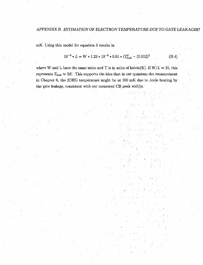
APPENDIX B. ESTIMATION OF ELECTRON TEMPERATURE DUE TO GATE LEAKAGE87
mK. Using this model for equation 3 results in
1(T9 * L = W * 1.23 * 1(T8 * 0.01 * (Tlak - (0.012)2 (B.4)
where W and L have the same units and T is in units of kelvin(K). If W/L « 10, this
represents Tieak ~ ZK. This supports the idea that in our quantum dot measurement
in Chapter 6, the 2DEG temperature might be at 100 mK due to Joule heating by
the gate leakage, consistent with our measured CB peak widths.
Bibliography
[1] S. Tarucha, D. G. Austing, T. Honda, R. J. van der Hage, and L. P. Kouwen-
hoven. Shell filling and spin effects in a few electron quantum dot. Phys. Rev.
Lett, 77(17):3613-3616, Oct 1996.
[2] D. Goldhaber-Gordon, H. Shtrikman, D. Mahalu, D. Abusch-Magder, U. Meirav,
and M. A. Kastner. Kondo effect in a single-electron transistor. Nature,
391(6663):156-159, 1998.
[3] E. Wigner. On the interaction of electrons in metals. Phys. Rev., 46(11):1002-
1011, Dec 1934.
[4] J. H. Davies. The Physics of Low-dimensional Semiconductors: An Introduction.
CUP, Cambridge, 1997.
[5] Y. Imry. Introduction to Mesoscopic Physics. Oxford University Press, Oxford,
1997.
[6] M. J. Manfra, K. W. Baldwin, A. M. Sergent, K. W. West, R. J. Molnar,
and J. Caissie. Electron mobility exceeding 160 000 cm2/V*s in AlGaN/GaN
heterostructures grown by molecular-beam epitaxy. Applied Physics Letters,
85(22):5394-5396, 2004.
[7] O. Ambacher, J. Smart, J. R. Shealy, N. G. Weimann, K. Chu, M. Murphy, W. J.
Schaff, L. F. Eastman, R. Dimitrov, L. Wittmer, M. Stutzmann, W. Rieger,
and J. Hilsenbeck. Two-dimensional electron gases induced by spontaneous and
piezoelectric polarization charges in N- and Ga-face AlGaN/GaN heterostruc
tures. Journal of Applied Physics, 85(6):3222-3233, 1999.
88
BIBLIOGRAPHY 89
[8] J. P. Ibbetson, P. T. Fini, K. D. Ness, S. P. DenBaars, J. S. Speck, and
U. K. Mishra. Polarization effects, surface states, and the source of electrons
in AlGaN/GaN heterostructure field effect transistors. Applied Physics Letters,
77(2):250-252, 2000.
[9] S. Syed, J. B. Heroux, Y. J. Wang, M. J. Manfra, R. J. Molnar, and H. L.
Stormer. Nonparabolicity of the conduction band of wurtzite GaN. Applied
Physics Letters, 83(22):4553-4555, 2003.
[10] W. Knap, E. Frayssinet, M. L. Sadowski, C. Skierbiszewski, D. Maude, V. Falko,
M. Asif Khan, and M. S. Shur. Effective g* factor of two-dimensional electrons in
GaN/AlGaN heterojunctions. Applied Physics Letters, 75(20):3156-3158, 1999.
[11] S. Schmult, M. J. Manfra, A. Punnoose, A. M. Sergent, K. W. Baldwin,
and R. J. Molnar. Large Bychkov-Rashba spin-orbit coupling in high-mobility
GaN/A^Gai-jcN heterostructures. Physical Review B (Condensed Matter and
Materials Physics), 74(3):033302, 2006.
[12] D. M. Zumbuhl, J. B. Miller, C. M. Marcus, K. Campman, and A. C. Gossard.
Spin-orbit coupling, antilocalization, and parallel magnetic fields in quantum
dots. Phys. Rev. Lett, 89(27):276803, Dec 2002.
[13] J. B. Miller, D. M. Zumbuhl, C. M. Marcus, Y. B. Lyanda-Geller, D. Goldhaber-
Gordon, K. Campman, and A. C. Gossard. Gate-controlled spin-orbit quantum
interference effects in lateral transport. Phys. Rev. Lett, 90(7):076807, Feb 2003.
[14] L.P. Kouwenhoven, CM. Marcus, P.L. McEuen, S. Tarucha, R.M. Westervelt,
and N.S. Wingreen. Mesoscopic electron transport. NATO Advanced Studies
Institute, Series E: Applied Science, 345:105-214, 1997.
[15] Y. Alhassid. The statistical theory of quantum dots. Rev. Mod. Phys., 72(4),
2000.
[16] I. L. Aleiner, P. W. Brouwer, and L. I. Glazman. Quantum effects in Coulomb
blockade. Phys. Rep., 358:309, 2002.

BIBLIOGRAPHY 90
[17] J. W. P. Hsu, M. J. Manfra, S. N. G. Chu, C. H. Chen, L. N. Pfeiffer, and
R. J. Molnar. Effect of growth stoichiometry on the electrical activity of screw
dislocations in GaN films grown by molecular-beam epitaxy. Applied Physics
Letters, 78(25):3980-3982, 2001.
[18] M. J. Manfra, N. G. Weimann, J. W. P. Hsu, L. N. Pfeiffer, K. W. West, S. Syed,
H. L. Stormer, W. Pan, D. V. Lang, S. N. G. Chu, G. Kowach, A. M. Sergent,
J. Caissie, K. M. Molvar, L. J. Mahoney, and R. J. Molnar. High mobility
AlGaN/GaN heterostructures grown by plasma-assisted molecular beam epitaxy
on semi-insulating GaN templates prepared by hydride vapor phase epitaxy.
Journal of Applied Physics, 92(1) :338-345, 2002.
[19] M. J. Biercuk, D. J. Monsma, C. M. Marcus, J. S. Becker, and R. G. Gordon.
Low-temperature atomic-layer-deposition lift-off method for microelectronic and
nanoelectronic applications. Applied Physics Letters, 83(12):2405-2407, 2003.
[20] B. J. van Wees, H. van Houten, C. W. J. Beenakker, J. G- Williamson, L. P.
Kouwenhoven, D. van der Marel, and C. T. Foxon. Quantized conductance of
point contacts in a two-dimensional electron gas. Phys. Rev. Lett, 60(9):848-850,
1988.
[21] D. A. Wharam, T. J. Thornton, R. Newbury, M. Pepper, H. Ahmed, J, E. F.
Frost, D. G. Hasko, D. C. Peacock, D. A. Ritchie, and G. A. C. Jones. One-
dimensional transport and the quantisation of the ballistic resistance. J. Phys.
C: Solid State Phys., 21:L209-L214, 1988.
[22] K. J. Thomas, J. T. Nicholls, M. Y. Simmons, M. Pepper, D. R. Mace, and D. A.
Ritchie. Possible spin polarization in a one-dimensional electron gas. Phys. Rev.
Lett, 77(1):135-138, 1996.
[23] K. S. Pyshkin, C. J. B. Ford, R. H. Harrell, M. Pepper, E. H. Linfield, and D. A.
Ritchie. Spin splitting of one-dimensional subbands in high quality quantum
wires at zero magnetic field. Phys. Rev. B, 434, 2005.
BIBLIOGRAPHY 91
[24] D. Tobben, D.A. Wharam, G. Abstreiter, J.P. Kolthaus, and F. Schaffler. Ballis
tic electron transport through a quantum point contact denned in a Si/Sio.7G0.3
heterostructure. Semiconductor Science and Technology, 10(5):711-714, 1995.
[25] U. Wieser, U. Kunze, K. Ismail, and J. O. Chu. Quantum-ballistic transport
in an etch-defined Si/SiGe quantum point contact. Applied Physics Letters,
81(9):1726-1728, 2002.
[26] S. J. Koester, C. R. Bolognesi, M. J. Rooks, E. L. Hu> and H. Kroemer. Quan
tized conductance of ballistic constrictions in InAs/AlSb quantum wells. Applied
Physics Letters, 62(12):1373-1375, 1993.
[27] O. Gunawan, B. Habib, E. P.-De Poortere, and M. Shayegan. Quantized con
ductance in an AlAs two-dimensional electron system quantum point contact.
Physical Review B (Condensed Matter and Materials Physics), 74(15):155436,
2006.
[28] I. Zailer, J. E. F. Frost, C. J. B. Ford, M. Pepper, M. Y. Simmons, D. A.
Ritchie, J. T. Nicholls, and G. A. C. Jones. Phase coherence, interference, and
conductance quantization in a confined two-dimensional hole gas. Phys. Rev. B,
49(7):5101-5104, Feb 1994.
[29] A. J. Daneshvar, C. J. B. Ford, A. R. Hamilton, M. Y. Simmons, M. Pepper, and
D. A. Ritchie. Enhanced g factors of a one-dimensional hole gas with quantized
conductance. Phys. Rev. B, 55(20):R13409-R13412, May 1997.
[30] L. P. Rokhinson, D. C. Tsui, L. N. Pfeiffer, and K. W. West. AFM local oxi
dation nanopatterning of a high mobility shallow 2d hole gas. Superlattices and
Microstructures, 32(2-3):99 - 102, 2002.
[31] R. Danneau, W. R. Clarke, O. Klochan, A. P. Micolich, A.! R. Hamilton, M. Y.
Simmons, M. Pepper, and D. A. Ritchie. Conductance quantization and the 0.7
x 2e2/h conductance anomaly in one-dimensional hole systems. Applied Physics
Letters, 88(1):012107, 2006.
BIBLIOGRAPHY 92
[32] J. Shabani, J. R. Petta, and M. Shayegan. High-quality quantum point contact in
two-dimensional GaAs (311) hole system. Applied Physics Letters, 93(21):212101,
2008.
[33] K. J. Thomas, J. T. Nicholls, N. J. Appleyard, M. Y. Simmons, M. Pepper, D. R.
Mace, W. R. Tribe, and D. A. Ritchie. Interaction effects in a one-dimensional
constriction. Phys. Rev. B, 58(8):4846-4852, Aug 1998.
[34] A. Kristensen, H. Bruus, A. E. Hansen, J. B. Jensen, P. E. Lindelof, C. J.
Marckmann, J. Nygard, C. B. S0rensen, F. Beuscher, A. Forchel, and M. Michel.
Bias and temperature dependence of the 0.7 conductance anomaly in quantum
point contacts. Phys. Rev. B, 62(16): 10950-10957, Oct 2000.
[35] S. M. Cronenwett, H. J. Lynch, D. Goldhaber-Gordon, L. P. Kouwenhoven, C. M.
Marcus, K. Hirose, N. S. Wingreen, and V. Umansky. Low-temperature fate of
the 0.7 structure in a point contact: A Kondo-like correlated state in an open
system. Phys. Rev. Lett, 88(22):226805-226808, 2002.
[36] N. K. Patel, J. T. Nicholls, L. Martn-Moreno, M. Pepper, J. E. F. Frost,
D. A. Ritchie, and G. A. C. Jones. Evolution of half plateaus as a function
of electric field in a ballistic quasi-one-dimensional constriction. Phys. Rev. B,
44(24):13549-13555, 1991.
[37] C. Siegert, Ghosh A., M. Pepper, I. Farrer, and D. A. Ritchie. The possibility of
an intrinsic spin lattice in high-mobility semiconductor heterostructures. Nature
Physics, 3:315-318, 2007.
[38] Amlan Majumdar. Spin polarization and enhancement of the effective g-factor
in one-dimensional electron systems with an in-plane magnetic field. Journal of
Applied Physics, 83(1):297-301, 1998.
[39] Alexander Struck, Siawoosh Mohammadi, Stefan Kettemann, and Bernhard
Kramer. Confinement-induced depletion of the enhanced g-factor in quan
tum wires. Physical Review B (Condensed Matter arid Materials Physics),
72(24):245317, 2005.

BIBLIOGRAPHY 93
[40] E. Koop, A. Lerescu, J. Liu, B. van Wees, D. Reuter, A. Wieck, and C. van der
Wal. The influence of device geometry on many-body effects in quantum point
contacts: Signatures of the 0.7 anomaly, exchange and kondo. Journal of Super
conductivity and Novel Magnetism, 20:433-441, 2007.
[41] Daniel Loss and David P. DiVincenzo. Quantum computation with quantum
dots. Phys. Rev. A, 57(1): 120-126, 1998.
[42] Ronald Potok and David Goldhaber-Gordon. Nanotechriology: New spin on
correlated electrons. Phys. Rev. B, 62(23):15842-15850, 2000.
[43] Boris Grbic, Renaud Leturcq, Klaus Ensslin, Dirk Reuter, and Andreas D.
Wieck. Single-hole transistor in p-type GaAs/AlGaAs heterostructures. Applied
Physics Letters, 87(23):232108-232110, 2005.
[44] Srinivasan Krishnamurthy, Mark van Schilfgaarde, and Nathan Newman. Spin
lifetimes of electrons injected into GaAs and GaN. Applied Physics Letters,
83:1761-1763, 2003.
[45] M. J. Manfra, K. W. Baldwin, A. M. Sergent, K. W. West, R. J. Molnar,
and J. Caissie. Electron mobility exceeding 160 000 cm2/V*s in AlGaN/GaN
heterostructures grown by molecular-beam epitaxy. Applied Physics Letters,
85(22):5394-5396, 2004.
[46] D. Abusch-Magder. Ph.D. thesis. Massachusetts Institute of Technology, 1997.
[47] E. B. Foxman, U. Meirav, P. L. McEuen, M. A. Kastner, O. Klein, P. A. Belk,
D. M. Abusch, and S. J. Wind. Crossover from single-level to multilevel transport
in artificial atoms. Phys. Rev. B, 50(19):14193-14199, Nov 1994.
[48] M.L. Mehta. Random Matrices. Boston: Academic Press, 1991.
[49] U. Sivan, R. Berkovits, Y. Aloni, O. Prus, A. Auerbach, and G. Ben-Yoseph.
Mesoscopic fluctuations in the ground state energy of disordered quantum dots,
Phys. Rev. Lett, 77(6):1123-1126, Aug 1996. :

BIBLIOGRAPHY 94
[50] F. Simmel, T. Heinzel, and D. A. Wharam. Statistics of conductance oscillations
of a quantum dot in the Coulomb-blockade regime. Europhys. Lett, 38:123-128,
1997.
[51] F. Simmel, David Abusch-Magder, D. A. Wharam, M. A. Kastner, and J. P.
Kotthaus. Statistics of the Coulomb-blockade peak spacings of a silicon quantum
dot. Phys. Rev. B, 59(16):R10441-R10444, Apr 1999.
[52] S. R. Patel, S. M. Cronenwett, D. R. Stewart, A. G. Huibers, C. M. Marcus, C. I.
Duruoz, J. S. Harris, K. Campman, and A. C. Gossard. Statistics of Coulomb
blockade peak spacings. Phys. Rev. Lett, 80(20):4522-4525, May 1998.
[53] S. Liischer, T. Heinzel, K. Ensslin, W. Wegscheider, and M. Bichler. Signatures
of spin pairing in chaotic quantum dots. Phys. Rev. Lett, 86(10):2118-2121, Mar
2001.
[54] Richard Berkovits. Absence of bimodal peak spacing distribution in the Coulomb
blockade regime. Phys. Rev. Lett, 81(10):2128-2131, Sep 1998.
[55] O. Prus, A. Auerbach, Y. Aloni, U. Sivan, and R. Berkovits. Even-odd correla
tions in capacitance fluctuations of quantum dots. Phys. Rev. B, 54(20) :R14289-
R14292, Nov 1996. ' ' • ' ' • , ' . '
[56] Denis Ullmo and Harold U. Baranger. Interactions in chaotic nanoparticles:
Fluctuations in coulomb blockade peak spacings. Phys, Rev. B, 64(24) :245324,
Dec 2001.
[57] Gonzalo Usaj and Harold U. Baranger. Spin and e — e interactions in quantum
dots: Leading order corrections to universality and temperature effects. Phys.
Rev. B, 66(15):155333, Oct 2002.
[58] Yuval Oreg, P. W. Brouwer, X. Waintal, and Bertrand I. Halperin. Spin, spin-
orbit, and electron-electron interactions in mesoscopic systems. arXiv.cond-
mat/0109541vl.
BIBLIOGRAPHY 95
[59] Raul O. Vallejos, Caio H. Lewenkopf, and Eduardo R. Mucciolo. Coulomb block
ade peak spacing fluctuations in deformable quantum dots: A further test of
random matrix theory. Phys. Rev. Lett, 81(3):677-680, Jul 1998.
[60] Y. Alhassid, Ph. Jacquod, and A. Wobst. Random matrix model for quantum
dots with interactions and the conductance peak spacing distribution. Phys. Rev.
B, 61(20):R13357-R13360, May 2000.
[61] Y. Alhassid and T. Rupp. A universal hamiltonian for a quantum dot in the
presence of spin-orbit interaction. arXiv:cond-mat/0312691vl, 200.
[62] Hong Jiang, Harold U. Baranger, and Weitao Yang. Spin and conductance-peak-
spacing distributions in large quantum dots: A density-functional theory study.
Phys. Rev. Lett, 90(2):026806, Jan 2003.
[63] Damir Herman, T. Tzen Ong, Gonzalo Usaj, Harsh Mathur, and Harold U.
Baranger. Level spacings in random matrix theory and coulomb blockade peaks
, in quantum dots. Physical Review B (Condensed Matter and Materials Physics),
76(19):195448, 2007.
[64] Ganpathy Murthy and R. Shankar. Quantum dots with disorder and interactions:
A solvable large-0 limit. Phys. Rev. Lett, 90(6):066801, Feb 2003.
[65] S. R. Patel, D. R. Stewart, C. M. Marcus, M. Gokcedag, Y. Alhassid, A. D.
Stone, C. I. Duruoz, and J. S. Harris Jr. Changing the electronic spectrum of a
quantum dot by adding electrons. Phys. Rev. Lett, 81(26):5900-5903, 1998.


![Transport properties and spin accumulation in ... · found in semiconductors with a two-dimensional electron gas (2DEG), opened a new area for spin-dependent electron transport [11]](https://img.pdfslide.us/doc/110x75/5f86494ce482b762c0713ef2/transport-properties-and-spin-accumulation-in-found-in-semiconductors-with-a.jpg)