Embed Size (px)
Citation preview
This document is downloaded from DR‑NTU (https://dr.ntu.edu.sg)Nanyang Technological University, Singapore.
Electrically pumped topological laser with valleyedge modes
Zeng, Yongquan; Chattopadhyay, Udvas; Zhu, Bofeng; Qiang, Bo; Li, Jinghao; Jin, Yuhao; Li,Lianhe; Davies, Alexander Giles; Linfield, Edmund Harold; Zhang, Baile; Chong, Yidong;Wang, Qi Jie
2020
Zeng, Y., Chattopadhyay, U., Zhu, B., Qiang, B., Li, J., Jin, Y., . . . Wang, Q. J. (2020).Electrically pumped topological laser with valley edge modes. Nature, 578(7794), 246–250.doi:10.1038/s41586‑020‑1981‑x
https://hdl.handle.net/10356/138755
https://doi.org/10.1038/s41586‑020‑1981‑x
© 2020 The Author(s). All rights reserved. This paper was published by Springer NatureLimited in Nature and is made available with permission of The Author(s).
Downloaded on 04 Nov 2021 09:29:37 SGT
1
Electrically Pumped Topological Laser with Valley Edge Modes
Yongquan Zeng1, Udvas Chattopadhyay2, Bofeng Zhu2, Bo Qiang1,2, Jinghao Li1, Yuhao Jin1,
Lianhe Li3, Alexander Giles Davies3, Edmund Harold Linfield3, Baile Zhang2*, Yidong Chong2*,
and Qi Jie Wang1,2*. 1Centre for OptoElectronics and Biophotonics, School of Electrical and Electronic Engineering & the
Photonic Institute, Nanyang Technological University, 50 Nanyang Avenue, Singapore 639798, Singapore 2Division of Physics and Applied Physics, School of Physical and Mathematical Sciences, Nanyang
Technological University, 21 Nanyang Link, Singapore 637371, Singapore. 3School of Electronic and Electrical Engineering, University of Leeds, Leeds LS2 9JT, U.K.
*e-mail: [email protected]; [email protected]; [email protected]
Quantum cascade lasers (QCLs) are compact electrically-pumped light sources in the
technologically important mid-infrared and terahertz (THz) region of the electromagnetic
spectrum1,2. Recently, the concept of topology3 has migrated from condensed matter physics
into photonics4, giving rise to a new type of lasing5–7 utilising topologically-protected photonic
modes that can efficiently bypass corners and defects4. Previous demonstrations of
topological lasers have required an external laser source for optical pumping, and operated
in the conventional optical frequency regime5–7. Here, we report on the first demonstration
of an electrically-pumped THz QCL based on topologically-protected valley edge states8–10.
Unlike previous topological lasers that relied on large-scale features to impart topological
protection, we employ a compact valley photonic crystal design9,10 analogous to two-
dimensional (2D) gapped valleytronic materials11. Lasing with regularly-spaced emission
peaks occurs in a sharp-cornered triangular cavity, even with the introduction of
perturbations, due to the existence of topologically-protected valley edge states that circulate
around the cavity without experiencing localisation. The properties of the topological lasing
modes are probed by adding different outcouplers to the topological cavity. This is the first
laser based on valley edge states and opens the door to practical use of topological protection
in electrically-driven laser sources.
Quantum cascade lasers (QCLs) are electrically-pumped semiconductor lasers based on
intersubband electron transitions in semiconductor multi-quantum-wells1,2. They are among the
most important sources of mid-infrared and terahertz (THz) radiation owning to their compactness,
high power, and high efficiency12,13. Their practical applications13 include telecommunication14,
THz signal processing15, imaging16, sensing, and spectroscopy. As with any laser, the emission
characteristics of a THz QCL depend on the design of the photonic cavity and are generally strongly
affected by the cavity shape17,18. One novel and highly-promising design element is the use of
topological edge states, which form running-wave modes that are robust against perturbations to
the underlying structure5–7, and can efficiently bypass defects (which may arise during fabrication
and packaging) and sharp corners. Unlike conventional waves, topological edge states resist the
2
formation of localised standing wave modes, which is helpful for suppressing the spatial hole-
burning effect19,20. This is a particularly important consideration for QCLs because their gain
recovery processes are faster than the carrier diffusion, unlike in traditional semiconductor lasers21.
Topological edge states arise at the interface between spatial domains that have topologically
distinct bandstructures3. There have been substantial efforts in recent years to implement such
states in photonics, motivated by potential applications for robust optical delay lines22, amplifiers23,
and other devices24,25. Topological lasers have been realized in one-dimensional (1D) Su-
Schrieffer-Heeger (SSH)-like systems26,27, whose edge states act as high-Q nanocavity modes that
lase under suitable gain. However, the edge states of 1D lattices do not support protected transport.
For two-dimensional (2D) lattices, realizing photonic topological edge states typically requires
some means of effective time-reversal (T) symmetry breaking to avoid the need to use magnetic
materials4. For example, the most recent demonstration of 2D topological lasing5,6 used an array of
ring resonators in which the clockwise or counterclockwise circulation of light in the resonators
acts as a photonic pseudospin; staggered inter-resonator couplings generate an effective magnetic
field and hence a T-broken bandstructure with nontrivial topology for each pseudospin22. This
design inherently requires large-scale structural features (e.g., ring resonators) far exceeding the
operating wavelength.
Valley photonic crystals (VPCs)9,10 are photonic analogues of 2D valleytronic materials11 that
host topological edge states protected by a valley degree of freedom established by the underlying
lattice symmetry. They have been demonstrated in a number of photonic crystal geometries28–30,
and similar valley-protected edge states have been realized in sonic crystals31. In 2D materials, the
valley degree of freedom can function similarly to spin in a spintronic device, but does not require
strong spin-orbit coupling11. Likewise, VPCs can provide robust light transport in highly compact
structures with periodicity on the order of the wavelength9,10, without the need for magnetic
materials or the complex construction of photonic pseudospins. They are therefore highly
promising for the implementation of compact topological photonic crystal lasers.
We have realized electrically-pumped THz QCLs utilising the topological edge states of a
VPC. Lasing is achieved using a topological waveguide that forms a triangular loop, very different
from conventional smoothly-shaped optical cavities. Despite the sharp corners of the cavity, we
find that the lasing spectrum exhibits robust regularly-spaced emission peaks, a feature that persists
under disturbances including: (i) a point outcoupling defect along an arm or corner of the triangle;
(ii) an array of outcoupling defects surrounding the triangle; and, (iii) an external waveguide acting
as a directional outcoupler. By exploring different configurations of defects and coupled
waveguides, we show that the various properties of the lasing modes can be explained by, and are
consistent with, the topological valley edge states of the VPC. We show that in a comparable cavity
based on a conventionally designed photonic crystal defect waveguide, the lasing modes behave
very differently: they tend to be localised and exhibit highly irregular mode spacings.
3
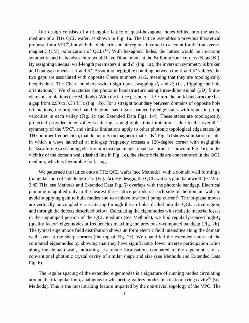
Our design consists of a triangular lattice of quasi-hexagonal holes drilled into the active
medium of a THz QCL wafer, as shown in Fig. 1a. The lattice resembles a previous theoretical
proposal for a VPC9, but with the dielectric and air regions inverted to account for the transverse-
magnetic (TM) polarization of QCLs1,2. With hexagonal holes, the lattice would be inversion
symmetric and its bandstructure would have Dirac points at the Brillouin zone corners (K and K′).
By assigning unequal wall-length parameters d1 and d2 (Fig. 1a), the inversion symmetry is broken
and bandgaps opens at K and K′. Assuming negligible coupling between the K and K′ valleys, the
two gaps are associated with opposite Chern numbers ±1/2, meaning that they are topologically
inequivalent. The Chern numbers switch sign upon swapping d1 and d2 (i.e., flipping the hole
orientations)9. We characterise the photonic bandstructure using three-dimensional (3D) finite-
element simulations (see Methods). With the lattice period a = 19.5 μm, the bulk bandstructure has
a gap from 2.99 to 3.38 THz (Fig. 1b). For a straight boundary between domains of opposite hole
orientations, the projected band diagram has a gap spanned by edge states with opposite group
velocities in each valley (Fig. 1c and Extended Data Figs. 1-4). These states are topologically
protected provided inter-valley scattering is negligible; this limitation is due to the overall T
symmetry of the VPC9, and similar limitations apply to other photonic topological edge states (at
THz or other frequencies), that do not rely on magnetic materials3. Fig. 1d shows simulation results
in which a wave launched at mid-gap frequency crosses a 120-degree corner with negligible
backscattering (a scanning electron microscope image of such a corner is shown in Fig. 1e). In the
vicinity of the domain wall (dashed line in Fig. 1e), the electric fields are concentrated in the QCL
medium, which is favourable for lasing.
We patterned the lattice onto a THz QCL wafer (see Methods), with a domain wall forming a
triangular loop of side length 21a (Fig. 2a). By design, the QCL wafer’s gain bandwidth (~ 2.95–
3.45 THz, see Methods and Extended Data Fig. 5) overlaps with the photonic bandgap. Electrical
pumping is applied only to the nearest three lattice periods on each side of the domain wall, to
avoid supplying gain to bulk modes and to achieve low total pump current6. The in-plane modes
are vertically outcoupled via scattering through the air holes drilled into the QCL active region,
and through the defects described below. Calculating the eigenmodes with realistic material losses
in the unpumped portion of the QCL medium (see Methods), we find regularly-spaced high-Q
(quality factor) eigenmodes at frequencies matching the previously-computed bandgap (Fig. 2b).
The typical eigenmode field distribution shows uniform electric field intensities along the domain
wall, even at the sharp corners (the top of Fig. 2c). We quantified the extended nature of the
computed eigenmodes by showing that they have significantly lower inverse participation ratios
along the domain wall, indicating less mode localisation, compared to the eigenmodes of a
conventional photonic crystal cavity of similar shape and size (see Methods and Extended Data
Fig. 6).
The regular spacing of the extended eigenmodes is a signature of running modes circulating
around the triangular loop, analogous to whispering-gallery modes in a disk or a ring cavity32 (see
Methods). This is the most striking feature imparted by the non-trivial topology of the VPC. The
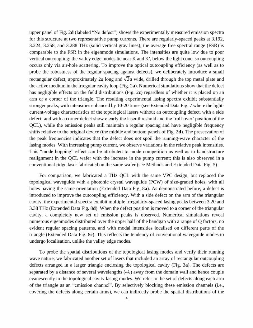
4
upper panel of Fig. 2d (labeled “No defect”) shows the experimentally measured emission spectra
for this structure at two representative pump currents. There are regularly-spaced peaks at 3.192,
3.224, 3.258, and 3.288 THz (solid vertical gray lines); the average free spectral range (FSR) is
comparable to the FSR in the eigenmode simulations. The intensities are quite low due to poor
vertical outcoupling: the valley edge modes lie near K and K′, below the light cone, so outcoupling
occurs only via air-hole scattering. To improve the optical outcoupling efficiency (as well as to
probe the robustness of the regular spacing against defects), we deliberately introduce a small
rectangular defect, approximately 2a long and √3a wide, drilled through the top metal plate and
the active medium in the irregular cavity loop (Fig. 2a). Numerical simulations show that the defect
has negligible effects on the field distributions (Fig. 2c) regardless of whether it is placed on an
arm or a corner of the triangle. The resulting experimental lasing spectra exhibit substantially
stronger peaks, with intensities enhanced by 10-20 times (see Extended Data Fig. 7 where the light-
current-voltage characteristics of the topological lasers without an outcoupling defect, with a side
defect, and with a corner defect show clearly the laser threshold and the ‘roll-over’ position of the
QCL), while the emission peaks still maintain a regular spacing and have negligible frequency
shifts relative to the original device (the middle and bottom panels of Fig. 2d). The preservation of
the peak frequencies indicates that the defect does not spoil the running-wave character of the
lasing modes. With increasing pump current, we observe variations in the relative peak intensities.
This “mode-hopping” effect can be attributed to mode competition as well as to bandstructure
realignment in the QCL wafer with the increase in the pump current; this is also observed in a
conventional ridge laser fabricated on the same wafer (see Methods and Extended Data Fig. 5).
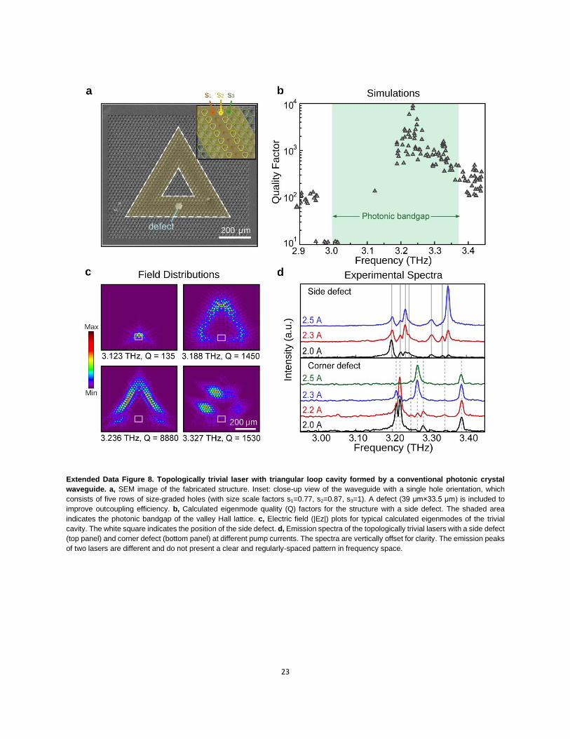
For comparison, we fabricated a THz QCL with the same VPC design, but replaced the
topological waveguide with a photonic crystal waveguide (PCW) of size-graded holes, with all
holes having the same orientation (Extended Data Fig. 8a). As demonstrated before, a defect is
introduced to improve the outcoupling efficiency. With a side defect on the arm of the triangular
cavity, the experimental spectra exhibit multiple irregularly-spaced lasing peaks between 3.20 and
3.38 THz (Extended Data Fig. 8d). When the defect position is moved to a corner of the triangular
cavity, a completely new set of emission peaks is observed. Numerical simulations reveal
numerous eigenmodes distributed over the upper half of the bandgap with a range of Q factors, no
evident regular spacing patterns, and with modal intensities localised on different parts of the
triangle (Extended Data Fig. 8c). This reflects the tendency of conventional waveguide modes to
undergo localisation, unlike the valley edge modes.
To probe the spatial distributions of the topological lasing modes and verify their running
wave nature, we fabricated another set of lasers that included an array of rectangular outcoupling
defects arranged in a larger triangle enclosing the topological cavity (Fig. 3a). The defects are
separated by a distance of several wavelengths (4) away from the domain wall and hence couple
evanescently to the topological cavity lasing modes. We refer to the set of defects along each arm
of the triangle as an “emission channel”. By selectively blocking these emission channels (i.e.,
covering the defects along certain arms), we can indirectly probe the spatial distributions of the
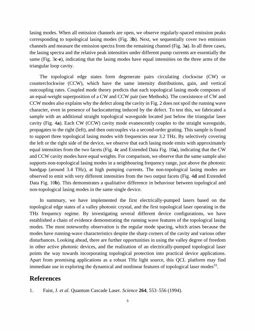
5
lasing modes. When all emission channels are open, we observe regularly-spaced emission peaks
corresponding to topological lasing modes (Fig. 3b). Next, we sequentially cover two emission
channels and measure the emission spectra from the remaining channel (Fig. 3a). In all three cases,
the lasing spectra and the relative peak intensities under different pump currents are essentially the
same (Fig. 3c-e), indicating that the lasing modes have equal intensities on the three arms of the
triangular loop cavity.
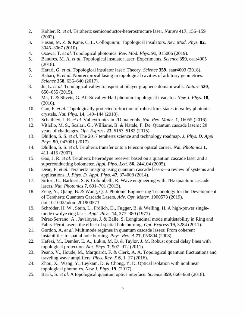
The topological edge states form degenerate pairs circulating clockwise (CW) or
counterclockwise (CCW), which have the same intensity distributions, gain, and vertical
outcoupling rates. Coupled mode theory predicts that each topological lasing mode composes of
an equal-weight superposition of a CW and CCW pair (see Methods). The coexistence of CW and
CCW modes also explains why the defect along the cavity in Fig. 2 does not spoil the running wave
character, even in presence of backscattering induced by the defect. To test this, we fabricated a
sample with an additional straight topological waveguide located just below the triangular laser
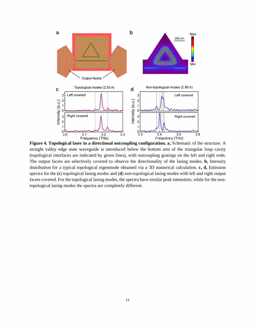
cavity (Fig. 4a). Each CW (CCW) cavity mode evanescently couples to the straight waveguide,
propagates to the right (left), and then outcouples via a second-order grating. This sample is found
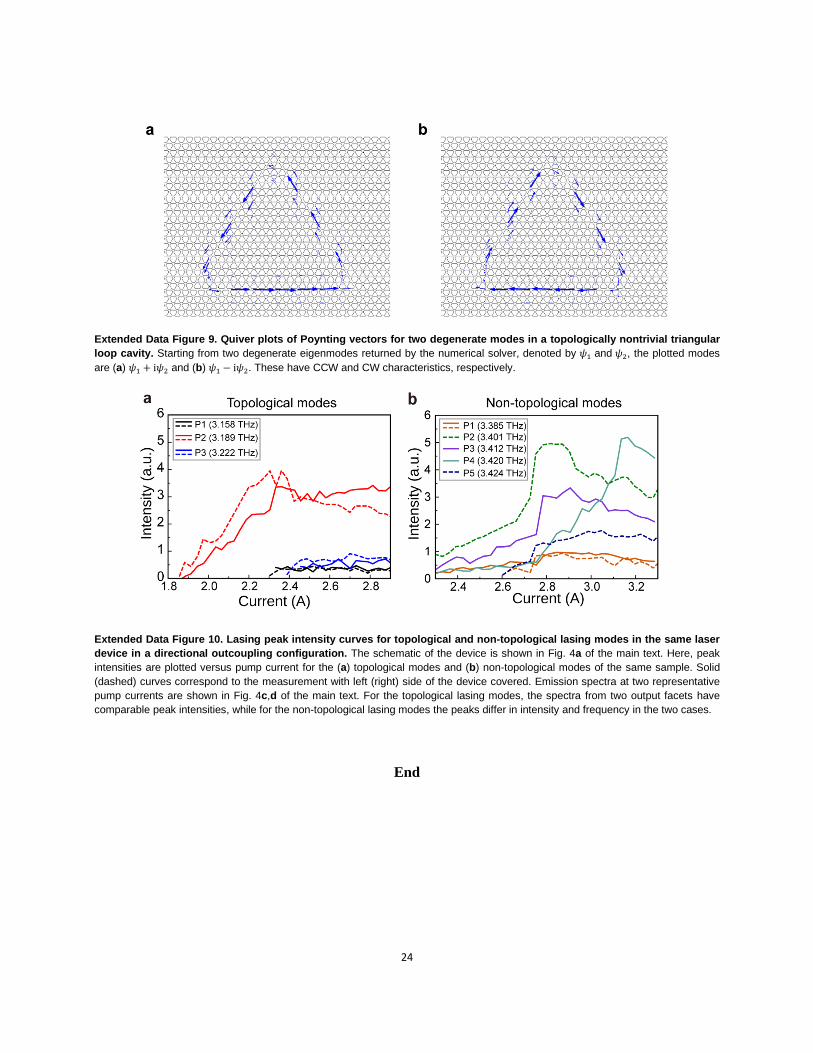
to support three topological lasing modes with frequencies near 3.2 THz. By selectively covering
the left or the right side of the device, we observe that each lasing mode emits with approximately
equal intensities from the two facets (Fig. 4c and Extended Data Fig. 10a), indicating that the CW
and CCW cavity modes have equal weights. For comparison, we observe that the same sample also
supports non-topological lasing modes in a neighbouring frequency range, just above the photonic
bandgap (around 3.4 THz), at high pumping currents. The non-topological lasing modes are
observed to emit with very different intensities from the two output facets (Fig. 4d and Extended
Data Fig. 10b). This demonstrates a qualitative difference in behaviour between topological and
non-topological lasing modes in the same single device.
In summary, we have implemented the first electrically-pumped lasers based on the
topological edge states of a valley photonic crystal, and the first topological laser operating in the
THz frequency regime. By investigating several different device configurations, we have
established a chain of evidence demonstrating the running wave features of the topological lasing
modes. The most noteworthy observation is the regular mode spacing, which arises because the
modes have running-wave characteristics despite the sharp corners of the cavity and various other
disturbances. Looking ahead, there are further opportunities in using the valley degree of freedom
in other active photonic devices, and the realization of an electrically-pumped topological laser
points the way towards incorporating topological protection into practical device applications.
Apart from promising applications as a robust THz light source, this QCL platform may find
immediate use in exploring the dynamical and nonlinear features of topological laser modes33.
References
1. Faist, J. et al. Quantum Cascade Laser. Science 264, 553–556 (1994).
6
2. Kohler, R. et al. Terahertz semiconductor-heterostructure laser. Nature 417, 156–159
(2002).
3. Hasan, M. Z. & Kane, C. L. Colloquium: Topological insulators. Rev. Mod. Phys. 82,
3045–3067 (2010).
4. Ozawa, T. et al. Topological photonics. Rev. Mod. Phys. 91, 015006 (2019).
5. Bandres, M. A. et al. Topological insulator laser: Experiments. Science 359, eaar4005
(2018).
6. Harari, G. et al. Topological insulator laser: Theory. Science 359, eaar4003 (2018).
7. Bahari, B. et al. Nonreciprocal lasing in topological cavities of arbitrary geometries.
Science 358, 636–640 (2017).
8. Ju, L. et al. Topological valley transport at bilayer graphene domain walls. Nature 520,
650–655 (2015).
9. Ma, T. & Shvets, G. All-Si valley-Hall photonic topological insulator. New J. Phys. 18,
(2016).
10. Gao, F. et al. Topologically protected refraction of robust kink states in valley photonic
crystals. Nat. Phys. 14, 140–144 (2018).
11. Schaibley, J. R. et al. Valleytronics in 2D materials. Nat. Rev. Mater. 1, 16055 (2016).
12. Vitiello, M. S., Scalari, G., Williams, B. & Natale, P. De. Quantum cascade lasers : 20
years of challenges. Opt. Express 23, 5167–5182 (2015).
13. Dhillon, S. S. et al. The 2017 terahertz science and technology roadmap. J. Phys. D. Appl.
Phys. 50, 043001 (2017).
14. Dhillon, S. S. et al. Terahertz transfer onto a telecom optical carrier. Nat. Photonics 1,
411–415 (2007).
15. Gao, J. R. et al. Terahertz heterodyne receiver based on a quantum cascade laser and a
superconducting bolometer. Appl. Phys. Lett. 86, 244104 (2005).
16. Dean, P. et al. Terahertz imaging using quantum cascade lasers—a review of systems and
applications. J. Phys. D. Appl. Phys. 47, 374008 (2014).
17. Sirtori, C., Barbieri, S. & Colombelli, R. Wave engineering with THz quantum cascade
lasers. Nat. Photonics 7, 691–701 (2013).
18. Zeng, Y., Qiang, B. & Wang, Q. J. Photonic Engineering Technology for the Development
of Terahertz Quantum Cascade Lasers. Adv. Opt. Mater. 1900573 (2019).
doi:10.1002/adom.201900573
19. Schröder, H. W., Stein, L., Frölich, D., Fugger, B. & Welling, H. A high-power single-
mode cw dye ring laser. Appl. Phys. 14, 377–380 (1977).
20. Pérez-Serrano, A., Javaloyes, J. & Balle, S. Longitudinal mode multistability in Ring and
Fabry-Pérot lasers: the effect of spatial hole burning. Opt. Express 19, 3284 (2011).
21. Gordon, A. et al. Multimode regimes in quantum cascade lasers: From coherent
instabilities to spatial hole burning. Phys. Rev. A 77, 053804 (2008).
22. Hafezi, M., Demler, E. A., Lukin, M. D. & Taylor, J. M. Robust optical delay lines with
topological protection. Nat. Phys. 7, 907–912 (2011).
23. Peano, V., Houde, M., Marquardt, F. & Clerk, A. A. Topological quantum fluctuations and
traveling wave amplifiers. Phys. Rev. X 6, 1–17 (2016).
24. Zhou, X., Wang, Y., Leykam, D. & Chong, Y. D. Optical isolation with nonlinear
topological photonics. New J. Phys. 19, (2017).
25. Barik, S. et al. A topological quantum optics interface. Science 359, 666–668 (2018).
7
26. St-Jean, P. et al. Lasing in topological edge states of a one-dimensional lattice. Nat.
Photonics 11, 651–656 (2017).
27. Zhao, H. et al. Topological hybrid silicon microlasers. Nat. Commun. 9, 1–6 (2018).
28. Dong, J. W., Chen, X. D., Zhu, H., Wang, Y. & Zhang, X. Valley photonic crystals for
control of spin and topology. Nat. Mater. 16, 298–302 (2017).
29. Kang, Y., Ni, X., Cheng, X., Khanikaev, A. B. & Genack, A. Z. Pseudo-spin–valley
coupled edge states in a photonic topological insulator. Nat. Commun. 9, 1–7 (2018).
30. Shalaev, M. I., Walasik, W., Tsukernik, A., Xu, Y. & Litchinitser, N. M. Robust
topologically protected transport in photonic crystals at telecommunication wavelengths.
Nat. Nanotechnol. 14, 31–34 (2019).
31. Lu, J. et al. Observation of topological valley transport of sound in sonic crystals. Nat.
Phys. 13, 369–374 (2017).
32. Sandoghdar, V. et al. Very low threshold whispering-gallery-mode microsphere laser.
Phys. Rev. A 54, R1777–R1780 (1996).
33. Seclì, M., Capone, M. & Carusotto, I. Theory of chiral edge state lasing in a two-
dimensional topological system. arXiv:1901.01290 (2019).
Acknowledgements
This work is supported by funding from the Ministry of Education, Singapore grant (MOE2016-
T2-1-128, MOE2016-T2-2-159) and National Research Foundation, Competitive Research
Program (NRF-CRP18-2017-02). U.C., Y.D.C, and B.L.Z. acknowledge support from the
Singapore Ministry of Education (MOE) Academic Research Fund Tier 2 Grants MOE2015-T2-
2-008 and MOE2018-T2-1-022 (S), and the Singapore Ministry of Education (MOE) Academic
Research Fund Tier 3 Grant MOE2016-T3-1-006. L.H.L., A.G.D., and E.H.L. acknowledge the
support of the EPSRC (UK) ‘HyperTerahertz programme (EP/P021859/1) and the Royal Society
and Wolfson Foundation.
Author contributions
Y.Q.Z. and B. Q. fabricated the laser devices. Y.Q.Z., J.H.L. and Y.H.J. performed the device
characterization. L.H.L., A.G.D., and E.H.L. performed QCL wafer growth. Y.Q.Z., U.C., and
B.F.Z. performed the simulations. Y.Q.Z., U.C., B.F.Z., B.L.Z., Y.D.C. and Q.J.W. performed
the theoretical analysis and contributed to manuscript preparation. B.L.Z., Y.D.C. and Q.J.W.
supervised the project.
Competing interests
The authors declare no competing financial interests.
Additional information
Supplementary information is available for this paper at doi:XXXX
8
Extended data is available for this paper at https://doi.org/xxx
Supplementary information is available for this paper at https://doi.org/ xxx
Reprints and permissions information is available at http://www.nature.com/ reprints.
Correspondence and requests for materials should be addressed to B.Z. or Y.C. or Q.J.W.
Publisher’s note: Springer Nature remains neutral with regard to jurisdictional claims in
published maps and institutional affiliations.
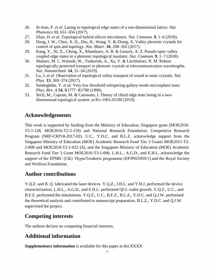
Figure 1. Design of a terahertz (THz) quantum cascade laser (QCL) with topologically-protected
valley edge modes. a, Each unit cell of the valley photonic crystal contains a quasi-hexagonal hole
perforated on a metal-semiconductor-metal heterostructure. The lattice period is a = 19.5 μm. b,
Bandstructure calculated by three-dimensional (3D) finite-element simulation. c, Projected band diagram
for a supercell representing a straight domain wall separating two domains with opposite hole orientations,
with 10 quasi-hexagonal holes on each side. d, Simulated electric field distribution (|Ez|) (top view and
cross section view) of a transmission mode in a topological waveguide with a 120-degree corner. The white
dashed line indicates the position of the cross-section view. e, Scanning electron microscope (SEM) image
of a portion of the fabricated topological waveguide near the corner, corresponding to the area enclosed by
a white rectangle in (d). Domain 1 and domain 2 have opposite orientations and thus, opposite valley Chern
numbers.
9
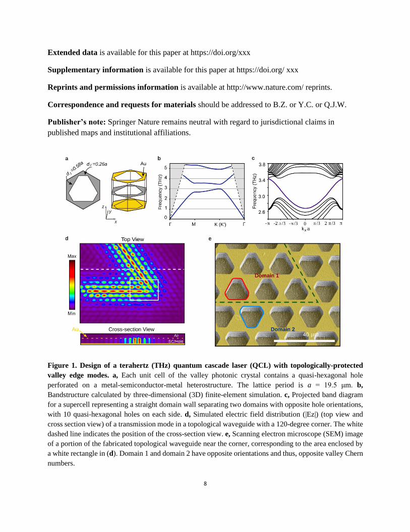
Figure 2. Fabrication and characterization of the topological THz QCL. a, SEM image of the THz QCL,
whose optical cavity consists of an in-plane triangular loop of a side length 21a. The shaded yellow area is
pumped by electrical injection, while the other parts are passive. The green dashed line indicates the domain
wall. The black rectangle indicates a defect (39 μm×33.5 μm) etched entirely through the active medium of
the THz QCL. Inset: cross-sectional schematic and magnified figure of the domain wall. b, Calculated
quality (Q) factors of the structure’s eigenmodes, with realistic material absorption losses (~ 20 cm-1) within
the passive region. The shaded area indicates the photonic bandgap of the valley Hall lattice. c, Typical
eigenmode electric field (|Ez|) profiles at around 3.23 THz, without an outcoupling defect, with a side defect,
and a corner defect. d, Emission spectra for the QCL without an outcoupling defect (top), with a side defect
(middle), and a corner defect (bottom). Gray vertical lines indicate the peak frequencies of the defect-free
QCL, which correspond closely to those of the QCL with a defect. The emission spectra are vertically offset
with increasing pumping intensities for clarity.
10
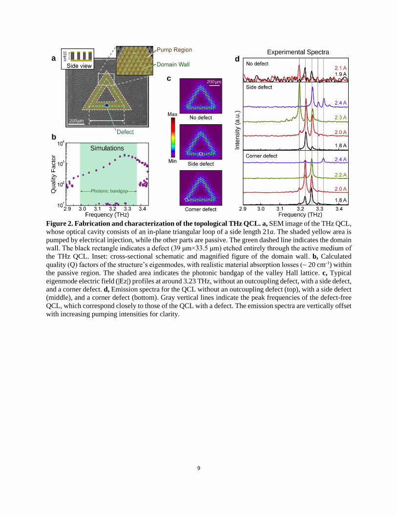
Figure 3. Topological laser with an array of evanescent outcouplers. a, Schematic of the structure. A
triangular loop cavity (green triangle) hosting topological edge states is surrounded by an array of
outcoupling defects (blue rectangles) distributed around the perimeter of a larger triangle. The defects are 8
lattice periods away from the topological interface, allowing for evanescent outcoupling. The inset shows
different defect-covering configurations for the spectral measurements. b, Emission spectra at different
pump currents (vertically shifted for clarity), with all defects uncovered. c, d, e, Emission spectra at various
pump currents for three different defect-covering configurations shown in the inset of (a).
11
Figure 4. Topological laser in a directional outcoupling configuration. a, Schematic of the structure. A
straight valley edge state waveguide is introduced below the bottom arm of the triangular loop cavity
(topological interfaces are indicated by green lines), with outcoupling gratings on the left and right ends.
The output facets are selectively covered to observe the directionality of the lasing modes. b, Intensity
distribution for a typical topological eigenmode obtained via a 3D numerical calculation. c, d, Emission
spectra for the (c) topological lasing modes and (d) non-topological lasing modes with left and right output
facets covered. For the topological lasing modes, the spectra have similar peak intensities, while for the non-
topological lasing modes the spectra are completely different.
12
Methods
1. Device fabrication, characterization and numerical simulations
We used terahertz (THz) quantum cascade laser (QCL) wafers with a three-well resonant-phonon
GaAs/Al0.15Ga0.85As design, with the gain curve spanning 2.95 to 3.45 THz34. The photonic crystal
structures were patterned onto the wafer with a standard metal-semiconductor-metal (MSM)
configuration35, as shown in Fig. 1a. The topological waveguide consists of quasi-hexagonal holes
with opposite orientations on either side of the topological interface, with wall lengths d1 = 0.58a
and d2 = 0.26a (or vice versa), where a = 19.5 μm is the lattice period. The outcoupling defect for
the sample shown in Fig. 2 consists of a rectangular hole with fixed size of 39 μm×33.5 μm. The
outcoupling defects for the sample shown in Fig. 3 consist of 12 rectangular holes of the same size,
uniformly distributed along three triangle arms and situated 8 lattice periods away from the
topological interface.
The fabrication process began with metal (Ti/Au 20/700 nm) deposition by an electron-beam
evaporator onto the THz QCL wafer and an n+-doped GaAs host substrate, followed by Au/Au
thermo-compression wafer bonding. Wafer polishing and selective wet etching
(NH3H2O/H2O2/H2O = 3/57/120) were sequentially conducted to remove the THz QCL substrate
down to an etch-stop layer. The etch-stop layer was then removed by hydrogen fluoride (49% cc.)
solution, and the QCL active region was exposed for subsequent microfabrication. A 300 nm SiO2
insulation layer was deposited onto the THz QCL wafer using plasma enhanced chemical vapor
deposition (PECVD), followed by optical lithography and reactive-ion etching (RIE) to define the
pumping area. The photonic structure patterns were transferred onto the THz QCL wafer by optical
lithography, with top metal (Ti/Au 20/900 nm) layer deposition and lift-off. With the top metal
layer as a hard mask, the photonic structures were formed by RIE dry etching through the active
region with a gas mixture of BCl3/CH4 = 100/20 sccm. The top metal layer (remnant thickness ~
300 nm) was retained as a top contact for current injection. The host substrate was covered by a
Ti/Au (15/200 nm) layer as bottom contact. Finally, the device chip was cleaved, indium-soldered
onto a copper heatsink, wire-bonded and attached to a cryostat cold finger for characterisation.
The fabricated THz laser devices were characterised using a Bruker Vertex 70 Fourier-
transform infrared spectrometer with a room-temperature deuterated-triglycine sulfate (DTGS)
detector. Mounted in a helium-gas-stream cryostat with temperature control at 9 K, the devices
were driven by a pulser with 10 kHz repetition rate and 500 ns pulse width. The emission signal
was captured by the detector in the vertical direction and Fourier-transformed into a spectrum, with
the spectrometer scanner velocity of 1 kHz and spectrum resolution of 0.2 cm-1. To measure the
emission from different outcouplers, e.g. the rectangular outcoupling defects or gratings, a thin
metal sheet (~ 100 μm) coated with an absorptive PMMA layer (~ 100 μm) was used to partially
cover the device emission surface partially. The absorption layer (single pass absorption rate ~
40%) was coated to reduce the light reflection from the metal sheet. The cover was positioned using
13
a custom stage with a positional accuracy of ~ 20 μm. The cover was placed very close to the
device surface: the gap between the device surface and the metal sheet was smaller than 300 μm.
In this work, all numerical results were calculated using the finite element method simulation
software COMSOL Multiphysics. In three-dimensional (3D) band diagram calculations, the 10-
μm-thick QCL medium was modeled as a lossless dielectric with a refractive index of 3.6,
sandwiched between metal layers modelled as perfect electrical conductors. All bandstructures
were computed for transverse-magnetic (TM) polarisation. The projected band diagram in Fig. 1c
was obtained with a supercell with 10 quasi-hexagonal holes on each side of the domain wall;
spurious modes localized at the boundaries of the computational cell were removed before plotting.
In 3D eigenmode calculations, the unpumped portion of the QCL medium was modelled as a lossy
dielectric, accounting for the intrinsic loss of the actual semiconductor medium; the imaginary part
of the refractive index is 0.0159, corresponding to an absorption loss ~ 20 cm-1. To reduce
computational workload, eigenmodes were computed for a slightly smaller structure with several
outermost unit cells removed, but with the triangular loop cavity left unchanged.
2. Valley photonic crystal design
Extended Data Fig. 1a shows the two-dimensional (2D) bandstructure of a triangular-lattice
photonic crystal whose unit cell comprises a regular hexagonal air holes in the dielectric of
refractive index 3.6. This dielectric medium represents the QCL wafer medium in the actual device.
The bandstructure exhibits Dirac points – linear band-crossing points between the two lowest TM
photonic bands – at the corners of the hexagonal Brillouin zone, denoted by K and K′. Near K (K′),
the Bloch states can be described by an effective 2D Dirac Hamiltonian36,37:
𝐻 = 𝑣𝐷(±𝑞𝑥𝜎𝑥 + 𝑞𝑦𝜎𝑦), (S1)
where �⃗� = (𝑞𝑥, 𝑞𝑦) is the wave-vector measured from K (K′), 𝑣𝐷is the group velocity, 𝜎𝑥,𝑦 are the
first two Pauli matrices, and the +(−) sign corresponds to K (K′).
Setting 𝑑1 ≠ 𝑑2 breaks the 𝐶3𝑣 symmetry of the photonic crystal, and lifts the degeneracy of
the Dirac points, as shown in Extended Data Fig. 1b. In Extended Data Fig. 1c,d, we plot the
absolute values of the out-of-plane electric field |𝐸𝑧| and Poynting vectors within each unit cell at
the K and K′ points for both the lower band and upper band. The modes in the two valleys are time-
reversed counterparts, as shown by the opposite circulations of electromagnetic power.
The effect of the symmetry-breaking can be modelled as a mass term added in the effective
Dirac Hamiltonian:
𝐻 = 𝑣𝐷(±𝑞𝑥𝜎𝑥 + 𝑞𝑦𝜎𝑦) + 𝑣𝐷𝑚𝜎𝑧, (S2)
14
where m represents the effective mass of Dirac particles, and 𝜎𝑧 is the third Pauli matrix. The
bandstructures near the two valleys (i.e., K and K′ ) have identical dispersion but are topologically
distinct. This can be shown by computing the valley-projected Chern number3, defined as
𝐶𝐾/𝐾′ =1
2∫ Ω𝐾/𝐾′( �⃗�)𝑑𝑆
𝐻𝐵𝑍, (S3)
where the integration is performed only for half of the Brillouin zone (HBZ) containing K or K′.
Here Ω𝐾/𝐾′(�⃗�) is the Berry curvature defined as Ω = ∇𝑘 × 𝐴(𝑘), where ∇𝑘= (𝜕
𝜕𝑘𝑥,
𝜕
𝜕𝑘𝑦). 𝐴(𝑘)
represents the Berry connection that is 𝐴𝑛(𝑘) = ∫ 𝑑2𝑟𝑢𝑘∗ (𝑟)∇𝑟𝑢𝑘(𝑟)
𝑈𝑛𝑖𝑡 𝑐𝑒𝑙𝑙, where ∇𝑟= (
𝜕
𝜕𝑥,
𝜕
𝜕𝑦),
and uk (r) represents the Bloch wavefunctions that can be calculated from numerical simulation.
Extended Data Fig. 2 shows the numerically calculated Berry curvature near K and K′ points,
whose integration over HBZ gives rise to opposite valley Chern numbers, i.e., 𝐶𝐾′ = 1/2 and 𝐶𝐾 =
−1/2. Rotating the quasi-hexagonal motif by 180° is equivalent to flipping the sign of the mass
parameter 𝒎, which flips the signs of the valley Chern numbers (𝐶𝐾′′ = −1/2, 𝐶𝐾
′ = 1/2).
Extended Data Fig. 3 shows a sample of photonic crystal consisting of two domains with
opposite valley Chern numbers. The differences in valley Chern numbers between the two domains
are
Δ𝐶𝐾 = 𝐶𝐾 − 𝐶𝐾 ′ = −1; Δ𝐶𝐾′ = 𝐶𝐾′ − 𝐶𝐾′
′ = +1. (S4)
Thus, based on the topological bulk-boundary correspondence principle3, there shall be one
forward-propagating edge state at K′ and one backward-propagating edge state at K. This is verified
by the numerically calculated photonic bandstructure shown in Extended Data Fig. 3b. The field
plots in Extended Data Fig. 3c, d show that the edge states are indeed strongly localized to the
domain wall, i.e. between the two domains with opposite valley Chern numbers.
3. Comparison of 2D and 3D bandstructures
In a 2D valley photonic crystal (VPC) with parameters stated in the main text, the bulk TM
bandstructure has a bandgap from 3.23 THz to 3.51 THz (the relative bandwidth of around 8%), as
shown by the black curves in Extended Data Fig. 4a. For a 2D structure with two domains of
opposite hole orientations separated by a straight domain wall (such as in Extended Data Fig. 3a),
the projected bandgap occupies a similar frequency range, and the valley edge states traverse the
whole projected bandgap as shown by the black curves in Extended Data Fig. 4b.
In the actual experiment, the VPC is 3D, patterned onto a THz QCL wafer in a MSM
configuration35. The active medium is 10 μm thick, sandwiched between two metal plates to ensure
subwavelength vertical confinement of the TM polarized lasing waves within the active layer.
Numerical results for the 3D structure are shown by the red curves in Extended Data Fig. 4. The
15
bandstructure and projected band diagram are shifted to lower frequencies, but otherwise remain
qualitatively similar.
4. Emission characteristics of conventional lasers (ridge laser and VPC laser)
In order to characterize the gain spectral range and other properties of the THz QCL wafer, we
fabricated and studied a conventional ridge laser. Extended Data Fig. 5a plots the emission spectra
at different pump currents. Upon scanning through the entire dynamic range of the pump, we
observe that the gain spectral range is approximately 2.95 THz to 3.45 THz. With increasing pump,
the emission spectrum envelop gradually blueshifts, which is due to the Stark shift of the
intersubband transition in the THz quantum cascade medium38,39.
To align the frequency of the VPC bandgap to the gain peak of the THz QCL (~ 2.9 THz–3.45
THz, evidenced by the range of emission peaks of the ridge laser), we fabricated a series of VPCs
of various periods without any domain wall loop cavity. By studying the lasing peaks, we
determined that the photonic bandgap of a VPC laser with a = 19.50 μm and size ~ 820 μm × 725
μm extends from 2.99 to 3.39 THz, which is a good match for the gain peak range of the THz QCL
wafer. These results also helped us to estimate the effective refractive index of the QCL active
region to be around 3.60 at the operation frequency.
5. Extended nature of topological modes
The key feature of the topological laser cavity is that it supports whispering-gallery-like running
wave modes even in presence of the three sharp corners. By contrast, a trivial cavity cannot support
such modes due to strong back-reflection at the corners, which localizes the electromagnetic field
at various portions of the cavity.
This phenomenon can be quantified by calculating the inverse participation ratio (IPR) along
the one-dimensional (1D) curve corresponding to the triangular loop. The IPR is widely used to
characterize the localization of modes and is defined as40
𝐼𝑃𝑅(𝜔) = ∫ |𝐸𝑧(𝜔,𝜉)|4
𝐿𝑑𝜉
[∫ |𝐸𝑧(𝜔,𝜉)|2𝐿 𝑑𝜉]
2 𝐿 , (S5)
where 𝜉 is the co-ordinate parametrizing the 1D curve of length 𝐿. The denominator in Eq. (S5)
ensures normalization. For a mode confined to a length 𝐿0, 𝐼𝑃𝑅 ~𝐿/𝐿0, whereas for completely
delocalized modes 𝐿0 ≈ 𝐿 ⇒ 𝐼𝑃𝑅 ≈ 1; with increasing localization, 𝐿0 decreases and therefore
the IPR increases.
The numerical IPR results for the triangular loop cavity are shown in Extended Data Fig. 6. As
expected, the topological modes have substantially smaller IPR than the non-topological modes.
6. Topological modes in the triangular loop cavity
16
Fig. 2b of the main text shows the numerically-calculated modes of a triangular cavity formed
between two topologically inequivalent VPC domains. These high-Q modes are constructed out of
topological edge states that have the characteristics of running waves.
From the condition that running waves should interfere constructively over each round trip, we
can estimate the mode separation or the free spectral range (FSR). Constructive interference
requires
Δ𝑘 =2π
𝐿 , (S6)
where 𝑘 denotes the wavenumber for the running-wave-like envelope function corresponding to
any given edge state, and L is the total path length (the circumference of the triangular loop). The
edge states have an approximately linear dispersion relation Δ𝜔 = 𝑣Δ𝑘, where 𝜔 is the angular
frequency detuning relative to mid-gap and 𝑣 is the group velocity. Hence, the FSR is
Δ𝑓 =𝑣
𝐿 . (S7)
For the structure, 𝐿 ≈ 1257 μ𝑚, and we estimate 𝑣 = 4.53 × 10⁷m/s from numerical calculations
(Fig. 1c). This yields Δ𝑓 ≈ 0.036 THz , which matches well with the simulations and the
experimental results (for example, Δ𝑓 = 0.035 THz for the simulation results shown in Fig. 2b,
and Δ𝑓 = 0.033 THz in the experimental results shown in Fig. 2d).
Due to time-reversal symmetry, each running wave mode has a degenerate counterpart with
opposite circulation direction. Hence, modes can be constructed from superpositions of clockwise
(CW) and counter-clockwise (CCW) running waves. Numerical solvers typically do not return the
CW and CCW solutions, but rather the superpositions of the two running waves. However, CW
and CCW modes can be reconstructed from suitable superpositions of the degenerate solutions
returned by the numerical solver (Extended Data Fig. 9).
The CW and CCW valley edge modes form two orthogonal basis modes and thus each
topological lasing mode is a superposition of CW and CCW valley edge modes41. To determine
the superpositions, we can use the framework of coupled-mode theory42. There are two important
effects acting on the CW and CCW modes: (i) weak coupling between CW and CCW modes,
induced for example by symmetry-breaking defects in the VPC, and (ii) gain and loss, which are
due to amplification by the gain medium, material dissipation, and radiative outcoupling.
Using coupled-mode theory, we represent the states of the laser by 𝜓 = (𝑎 𝑏)𝑇, where 𝑎 and 𝑏
are the CW and CCW mode amplitudes respectively. The condition for steady-state lasing is
𝐻0𝜓 + 𝑖 (𝑔
1+|𝜓|2 − 𝛾) 𝜓 = 𝛿𝜔 𝜓, (S8)
where
17
𝐻0 = [0 −𝜅
−𝜅 0]
is a Hermitian Hamiltonian containing a coupling rate 𝜅 between the CW and CCW modes, both
of which have zero frequency detuning, 𝛿𝜔 is the frequency detuning of the steady-state lasing
mode, 𝑔 is the amplification rate due to the gain medium, and 𝛾 is the loss rate due to material
dissipation and radiative outcoupling. Note that the gain is saturable.
Importantly, the non-Hermitian terms are diagonal because the CW and CCW modes are
topologically protected running waves that have the same intensity distribution, and therefore
should experience the same rates of gain and loss.
Regardless of the non-Hermitian terms, the solutions to the coupled-mode equation are
𝜓 ∝1
√2(1 1)𝑇 for 𝛿𝜔 = +𝜅,
𝜓 ∝1
√2(1 − 1)𝑇 for 𝛿𝜔 = −𝜅. (S9)
In other words, the CW and CCW modes should contribute equally to the steady-state lasing mode.
The overall amplitude can be determined by setting the imaginary part of the eigenproblem to zero.
These results hold not only at the lasing threshold, but also in the above-threshold regime where
gain saturation is in effect. Above threshold, provided 𝜅 is not too large, a single steady-state lasing
mode is spontaneously chosen from one of the two possible solutions solved above, and the other
solution is suppressed (i.e., its amplitude is pinned to zero) by gain competition.
The above analysis rests on the idea that the underlying a and b modes are counter-propagating
topological modes. It does not apply if the modes experience different gain/loss rates (so that the
non-Hermitian term is non-diagonal), or if they are non-degenerate – as is the case in the non-
topological cavity, which lacks running-wave-like edge states.
7. Bi-directional outcoupling of laser modes
Here, we provide more details about the topological laser in the directional coupling configuration
(Fig. 4 of the main text and Extended Data Fig. 10).
This structure features a straight topological waveguide placed below the triangular cavity (Fig.
4a). The valley Chern number difference along the straight waveguide is opposite to that along the
bottom arm of the triangular cavity. Due to valley conservation, a CW (CCW) cavity mode
evanescently couples to a right (left) moving valley edge mode on the straight waveguide. The
output facets on the left and right ends of the straight waveguide are second-order gratings. After
using numerical simulations to optimise the grating parameters, the reflection ratio is estimated to
be < 10%, ensuring negligible light feedback into the straight waveguide and laser cavity.
18
Numerical simulations of the structure reveal topological eigenmodes at frequencies near 3.2
THz, within the topological gap of the VPC. The intensity plot for a typical eigenmode is shown
in Fig. 4b. These numerically-calculated topological eigenmodes are all twofold degenerate,
consistent with the degenerate CW and CCW cavity modes of the triangular loop. Moreover, the
structure hosts non-topological lasing modes around 3.4 THz, around the edge of the upper band.
The non-topological modes are all non-degenerate.
In the experiment, each topological mode exhibits a “peak ratio” (the ratio of emission peak
intensities from two output facets) close to unity. A typical spectrum is shown in Fig. 4c, and the
light-current curves are shown in Extended Data Fig. 10a. For the non-topological modes, the peak
ratios are far from unity (Fig. 4d and Extended Data Fig. 10b); for some of these, the peak is only
clearly observable when one facet is covered but lies within the noise floor when the other facet is
covered.
During repeated experimental runs with the same sample, we observe a repeatable set of peak
frequencies for both the topological and non-topological lasing modes, but the exact peak
intensities vary between runs due to the imprecise relative alignment of the covering metal sheet
and sample. We observe that the topological modes have peak ratios close to unity, whereas the
non-topological modes have different peak ratios.
Method references
34. Belkin, M. et al. High-temperature operation of terahertz quantum cascade laser sources.
IEEE J. Sel. Top. Quantum Electron. 15, 952–967 (2009).
35. Williams, B. S., Kumar, S., Callebaut, H., Hu, Q. & Reno, J. L. Terahertz quantum-
cascade laser at λ≈100 μm using metal waveguide for mode confinement. Appl. Phys. Lett.
83, 2124–2126 (2003).
36. Gao, Z. et al. Valley surface-wave photonic crystal and its bulk/edge transport. Phys. Rev.
B 96, 1–6 (2017).
37. Wu, X. et al. Direct observation of valley-polarized topological edge states in designer
surface plasmon crystals. Nat. Commun. 8, (2017).
38. Vitiello, M. S. & Tredicucci, A. Tunable Emission in THz Quantum Cascade Lasers. IEEE
Trans. Terahertz Sci. Technol. 1, 76–84 (2011).
39. Fathololoumi, S. et al. Terahertz quantum cascade lasers operating up to ~ 200 K with
optimized oscillator strength and improved injection tunneling. Opt. Express 20, 3331–
3339 (2012).
40. Rockstuhl, C. & Scharf, T. Amorphous Nanophotonics. (Springer Science & Business
Media, 2013).
19
41. Spreeuw, R. J. C., Neelen, R. C., van Druten, N. J., Eliel, E. R. & Woerdman, J. P. Mode
coupling in a He-Ne ring laser with backscattering. Phys. Rev. A 42, 4315–4324 (1990).
42. Wang, Z., Fan, S. & Suh, W. Temporal coupled-mode theory and the presence of non-
orthogonal modes in lossless multimode cavities. IEEE J. Quantum Electron. 40, 1511–
1518 (2004).
Data availability statement
The datasets generated during and/or analysed during the current study are available in the DR-
NTU(Data) repository [https://doi.org/10.21979/N9/PECAGQ].
Extended data
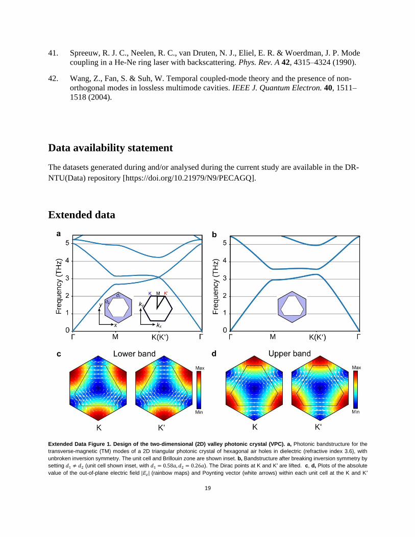
Extended Data Figure 1. Design of the two-dimensional (2D) valley photonic crystal (VPC). a, Photonic bandstructure for the
transverse-magnetic (TM) modes of a 2D triangular photonic crystal of hexagonal air holes in dielectric (refractive index 3.6), with
unbroken inversion symmetry. The unit cell and Brillouin zone are shown inset. b, Bandstructure after breaking inversion symmetry by
setting 𝑑1 ≠ 𝑑2 (unit cell shown inset, with 𝑑1 = 0.58𝑎, 𝑑2 = 0.26𝑎). The Dirac points at K and K′ are lifted. c, d, Plots of the absolute
value of the out-of-plane electric field |𝐸𝑧| (rainbow maps) and Poynting vector (white arrows) within each unit cell at the K and K′
20
points. For both the (c) lower band and (d) upper band, the modes in the two valleys are time-reversed counterparts, as shown by the
opposite circulations of electromagnetic power.
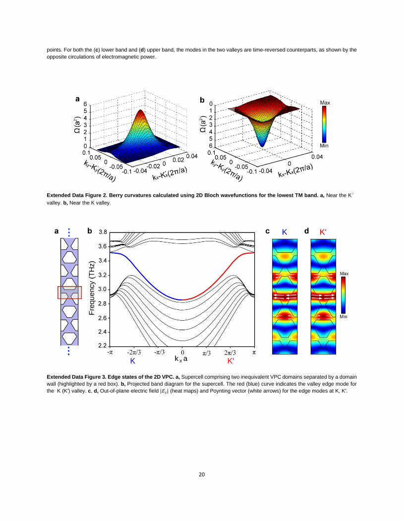
Extended Data Figure 2. Berry curvatures calculated using 2D Bloch wavefunctions for the lowest TM band. a, Near the K′
valley. b, Near the K valley.
Extended Data Figure 3. Edge states of the 2D VPC. a, Supercell comprising two inequivalent VPC domains separated by a domain
wall (highlighted by a red box). b, Projected band diagram for the supercell. The red (blue) curve indicates the valley edge mode for
the K (K′) valley. c, d, Out-of-plane electric field |𝐸𝑧| (heat maps) and Poynting vector (white arrows) for the edge modes at K, K′.
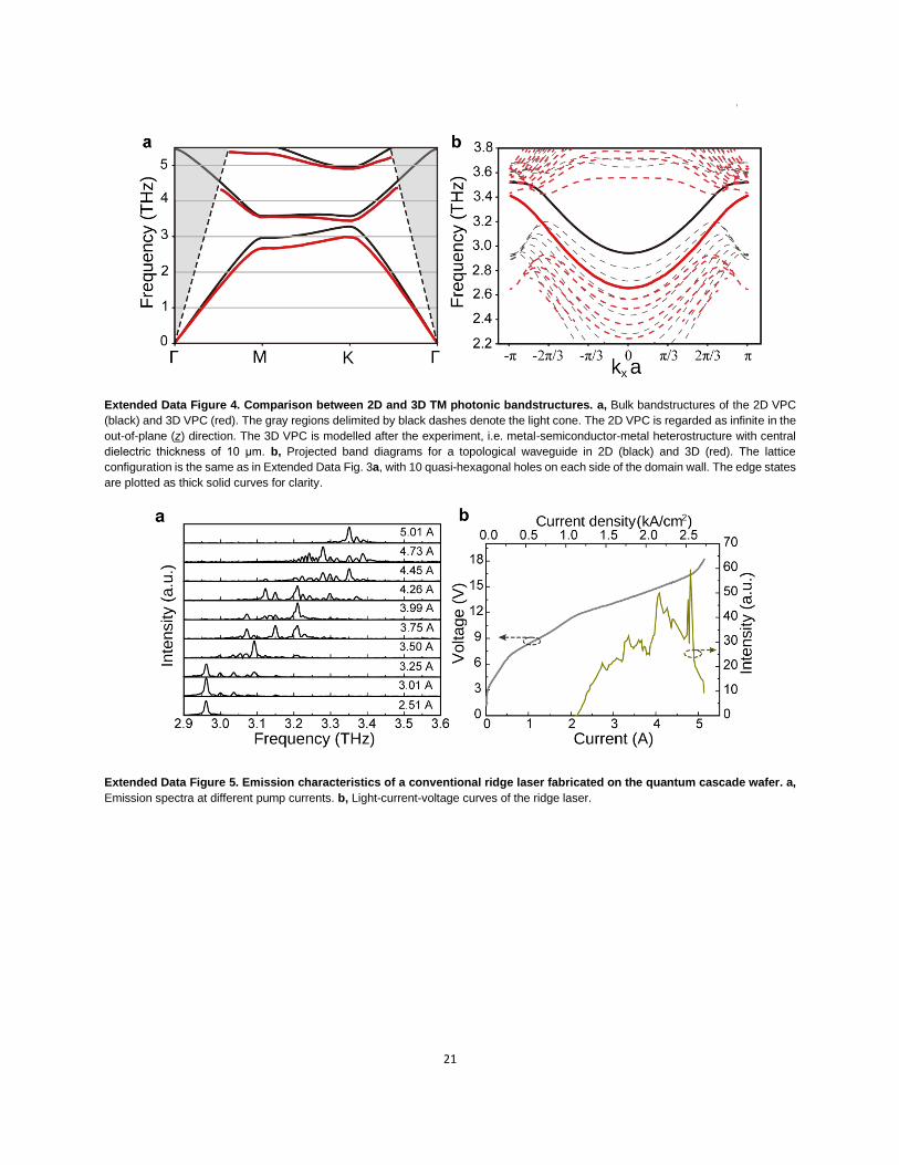
21
Extended Data Figure 4. Comparison between 2D and 3D TM photonic bandstructures. a, Bulk bandstructures of the 2D VPC
(black) and 3D VPC (red). The gray regions delimited by black dashes denote the light cone. The 2D VPC is regarded as infinite in the
out-of-plane (z) direction. The 3D VPC is modelled after the experiment, i.e. metal-semiconductor-metal heterostructure with central
dielectric thickness of 10 μm. b, Projected band diagrams for a topological waveguide in 2D (black) and 3D (red). The lattice
configuration is the same as in Extended Data Fig. 3a, with 10 quasi-hexagonal holes on each side of the domain wall. The edge states
are plotted as thick solid curves for clarity.
Extended Data Figure 5. Emission characteristics of a conventional ridge laser fabricated on the quantum cascade wafer. a,
Emission spectra at different pump currents. b, Light-current-voltage curves of the ridge laser.
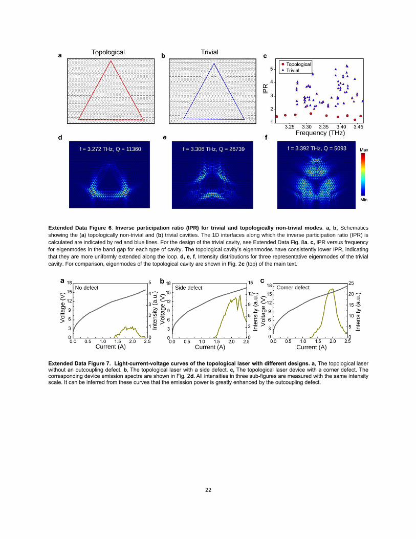
22
Extended Data Figure 6. Inverse participation ratio (IPR) for trivial and topologically non-trivial modes. a, b, Schematics
showing the (a) topologically non-trivial and (b) trivial cavities. The 1D interfaces along which the inverse participation ratio (IPR) is
calculated are indicated by red and blue lines. For the design of the trivial cavity, see Extended Data Fig. 8a. c, IPR versus frequency
for eigenmodes in the band gap for each type of cavity. The topological cavity’s eigenmodes have consistently lower IPR, indicating
that they are more uniformly extended along the loop. d, e, f, Intensity distributions for three representative eigenmodes of the trivial
cavity. For comparison, eigenmodes of the topological cavity are shown in Fig. 2c (top) of the main text.
Extended Data Figure 7. Light-current-voltage curves of the topological laser with different designs. a, The topological laser without an outcoupling defect. b, The topological laser with a side defect. c, The topological laser device with a corner defect. The corresponding device emission spectra are shown in Fig. 2d. All intensities in three sub-figures are measured with the same intensity scale. It can be inferred from these curves that the emission power is greatly enhanced by the outcoupling defect.
23
Extended Data Figure 8. Topologically trivial laser with triangular loop cavity formed by a conventional photonic crystal
waveguide. a, SEM image of the fabricated structure. Inset: close-up view of the waveguide with a single hole orientation, which
consists of five rows of size-graded holes (with size scale factors s1=0.77, s2=0.87, s3=1). A defect (39 μm×33.5 μm) is included to
improve outcoupling efficiency. b, Calculated eigenmode quality (Q) factors for the structure with a side defect. The shaded area
indicates the photonic bandgap of the valley Hall lattice. c, Electric field (|Ez|) plots for typical calculated eigenmodes of the trivial
cavity. The white square indicates the position of the side defect. d, Emission spectra of the topologically trivial lasers with a side defect
(top panel) and corner defect (bottom panel) at different pump currents. The spectra are vertically offset for clarity. The emission peaks
of two lasers are different and do not present a clear and regularly-spaced pattern in frequency space.
24
Extended Data Figure 9. Quiver plots of Poynting vectors for two degenerate modes in a topologically nontrivial triangular
loop cavity. Starting from two degenerate eigenmodes returned by the numerical solver, denoted by 𝜓1 and 𝜓2, the plotted modes
are (a) 𝜓1 + i𝜓2 and (b) 𝜓1 − i𝜓2. These have CCW and CW characteristics, respectively.
Extended Data Figure 10. Lasing peak intensity curves for topological and non-topological lasing modes in the same laser
device in a directional outcoupling configuration. The schematic of the device is shown in Fig. 4a of the main text. Here, peak
intensities are plotted versus pump current for the (a) topological modes and (b) non-topological modes of the same sample. Solid
(dashed) curves correspond to the measurement with left (right) side of the device covered. Emission spectra at two representative
pump currents are shown in Fig. 4c,d of the main text. For the topological lasing modes, the spectra from two output facets have
comparable peak intensities, while for the non-topological lasing modes the peaks differ in intensity and frequency in the two cases.
End

25