Embed Size (px)
Citation preview
Vacuum 64 (2002) 307–313
Electrical simulation of a p–i–n image sensor
J. Martins*, M. Fernandes, M. Vieira
Electronics and Communications Department, ISEL, Rua Conselheiro Em!ııdio Navarro 1, 1949-014 Lisbon, Portugal
Abstract
We have modelled a p–i–n image sensor under local illumination through a two-dimensional non-linear circuit. The
sensor is described as an array of photodiodes interconnected through lateral resistors, which model the sheet resistance
of the doped layers. Under small-signal analysis, each photodiode is modelled by a current-controlled resistor
proportional to the inverse of the photocurrent. A SPICE based simulator is used to analyse the sensor output
characteristics.
Several configurations and contact geometries are analysed for the image transducer. The image responsivity, the
spatial resolution and the image distortion are modelled by changing the ratio between the transversal and the lateral
resistors or the acquisition points. Results show that the geometry and location of the contacts affect the distortion of
the restored image. The conductivity of the doped layers and the light flux illumination influences the image resolution
and accuracy. The simulated and experimental results were found in a good agreement. r 2002 Elsevier Science Ltd.
All rights reserved.
Keywords: Semiconductor device modelling; Electrical modelling of p–i–n devices; Electrical simulation; Optical sensors; Image
acquisition and representation
1. Introduction
An electrical model for a device comes first
from the simple theory of the device, trying to
capture its basic operation features. Subsequently,
the model is enhanced from the feedback of
experimental results. At the same time, some
of the sensor characteristics may be improved
using the insight obtained from simulation
results.
SPICE [1] is the de facto industrial standard
for computer-aided circuit analysis, including
models of semiconductor devices: p–n junct-
ion diode, bipolar junction transistor, field
effect transistor, etc. Usually, a general-purpose
circuit simulator using SPICE performs three
main types of analysis: non-linear dc, non-
linear transient, and linear small-signal ac
analysis.
Electrical simulation is a helpful tool to get
insight into the physical model of a semiconductor
imager. An electrical simulation based on SPICE
program was used to describe and analyse the
image sensor performance. Several configurations
of the sensor were analysed: contact geometry,
n-layer conductivity, and image intensity levels.
Results from simulation are supported by experi-
mental results.
*Corresponding author. Tel.: +351-21-8317289; fax: +351-
21-8317114.
E-mail address: [email protected] (J. Martins).
0042-207X/02/$ - see front matter r 2002 Elsevier Science Ltd. All rights reserved.
PII: S 0 0 4 2 - 2 0 7 X ( 0 1 ) 0 0 3 0 6 - 2

2. Sensor structure and simulation model
2.1. Sensor configuration and operation
Large area image transducers in the assembly
glass/ZnO : Al//pS a-Si : H//iS a-Si : H//nS a-
SixC1�x : H/Al [2] are modelled and studied by
means of an electrical simulation. The sensor is a
two dimensional structure composed of a p–i–n
photodiode (the active element) and front and
back contacts that are used as electrical interface.
In Fig. 1 the geometrical configuration as well as
the electrical model proposed are depicted.
The p–i–n experimental transducers were de-
posited by plasma enhanced chemical vapour
deposition at a 13.56 MHz radio frequency and
the contacts deposited by thermal evaporation.
Deposition conditions, experimental details and
sensor performance are described elsewhere [2,3].
A focused image, constituted by a steady-state
light, is projected onto a fixed location in the
photosensitive surface, through the transparent
contact. For image acquisition, a low-power
chopped laser spot scans the sensor in the frame
mode. The read-out of the injected carriers is
achieved by measuring the ac component of the
short circuit current, Isc: It was shown that the
output signal depends on the photocurrent pro-
duced by the image, Idc; as much as by the one
produced by the scanner, Iac [4].
The methodology used for image representation
is explained through a modulation of the potential
barrier due to the local steady-state illumination of
the junction. Here, due to the higher conductivity
of the doped layer, the photogenerated minority
carriers build up across all the active surface, while
the majority carriers are accumulated in the
illuminated region, beyond the depletion layer
edge, causing a reduction in the band bending
across this region [5]. If, in addition, a weak light
spot is scanning the device, in the dark regions the
carriers generated by the scanner are separated by
the junction electric field and collected (high ac
component of the current). Those generated inside
the illuminated regions can drift in the lateral
direction, due to the local lowering of the potential
barrier, and recombine inside the amorphous bulk
(low ac component of the current). So, illuminated
regions are ascribed to low ac components of the
photocurrent, and dark regions to high ac photo-
current values.
All the image acquisition process is performed
by storing the current values as a two dimensional
array of discrete values, Im;n; each one representing
the photocurrent induced by the chopped light at
the selected m� n position. The image intensity is
obtained by subtracting the input matrix Im;n (with
image) from the background, bm;n (without image)
and inverting the results.
2.2. Electrical model
In operation, a photodiode can be represented
by a photogenerated current source feeding into an
ideal diode, and its internal characteristics are best
modelled by the introduction of a shunt resistor, a
shunt capacitor and a series resistor [6]. For large
signal or dc mode, the photodiode is modelled as a
non-linear current source, ID; that depends on the
photocurrent, Iph; and on the voltage across the
diode, VD; through ID ¼ IS½expðVD=ZVT Þ � 1Þ� �Iph; with IS the saturation current, Z the ideality
factor of the diode, and VT the thermal voltage.
However, under small-signal conditions, the
photodiode is a non-linear photocurrent-con-
trolled resistor (rd), which represents an incre-
mental resistance, around the quiescent operating
point and is expressed in terms of Iph as 1=rd ¼@ID=@VDEIph=ZVT :
The electrical model for the p–i–n image sensor
can be an array of photodiodes intercon-
nected through lateral resistors [7] (see Fig. 1).
Each photodiode is replaced by its incrementalFig. 1. Sensor configuration and electrical model.
J. Martins et al. / Vacuum 64 (2002) 307–313308
resistance and connected to its four neighbours, in
a row-line matrix, by resistors: RLn and RLp that
model the sheet resistance of the n- and p-doped
layers, respectively. The contacts may have differ-
ent configurations and establish the points for
transversal measurements. The image pattern is
reconstructed from the photovoltage readout in
the same way as described in Section 2.1.
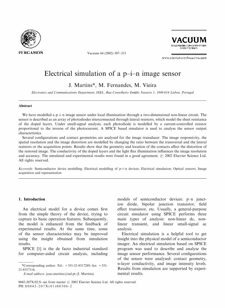
2.3. Simulation analysis
Simulation results were obtained using a
SPICE-based simulator. Fig. 2 shows a fraction
of the electrical circuit, being part of the non-
planar structure used for simulation. One can
depict the diodes (D), the lateral (RL) and
transversal (rd) resistors, the scanner source (Is),and a point of voltage measurement (V).
The scanner is a sine-wave current source
(0.1 mA, 10 Hz) applied from each top node of
the circuit to the ground or reference point. Those
nodes are the diode anodes, corresponding to the
m� n points for voltage read-out.
Different contact geometry configurations can
be used: strips at the structure borders or large
area contacts covering the entire active surface. In
the simulation circuit the contact shaping is
achieved by choosing the points for voltage read-
out: the measurement point (V) and the ground or
reference point. For the case where the contacts
are localised at the structure borders, the measure-
ment and ground points are fixed at circuit nodes
representing the contact regions where the lateral
resistors (RL) are short-circuited. For large area
contacts, the voltage measurement points change
for each m� n value read-out, as is shown in
Fig. 2.
Several p–i–n sensors with different n-layer
conductivity were also simulated. This was
achieved by changing RL for the whole circuit,
accordingly. Higher conductivities correspond to
lower values of RL: Also, different image intensity
levels were analysed, changing rd on points
allocated to the image area.
2.4. Simulation procedure
The simulation procedure has two phases, the
circuit construction and the simulation process.
The first phase has three steps. In the first step, the
array dimension is chosen. The number of lines
and rows in the circuit of Fig. 2 depend on the
image shape, and their number is chosen in order
to have enough nodes to include the image area
and a surrounding dark region. This region is
made large enough to accommodate the contact
regions and suppress the influence from the
structure border. The second step is to choose
the points of measurement, accordingly the con-
tact geometry. In the third step the circuit nodes
are allocated to image positions and the values for
rd ;RLn and RLp are chosen.
In the second phase, a voltage distribution
composed of a matrix of m� n values is obtained.
Each simulation run corresponds to a different
assigned node where the scanner source is applied.
The stored values are the amplitudes of the
sinusoidal small signals taken in each simulation
process step. The image intensity matrix is
obtained as described in Section 2.2.
3. Results and discussion
3.1. Contact geometry versus blurring effect
The contact geometry is an important parameter
to define accurately the image. Several contact
geometry configurations were analysed [8].Fig. 2. Electrical circuit for simulation.
J. Martins et al. / Vacuum 64 (2002) 307–313 309
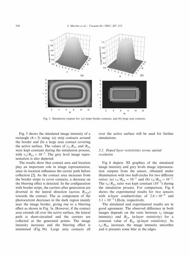
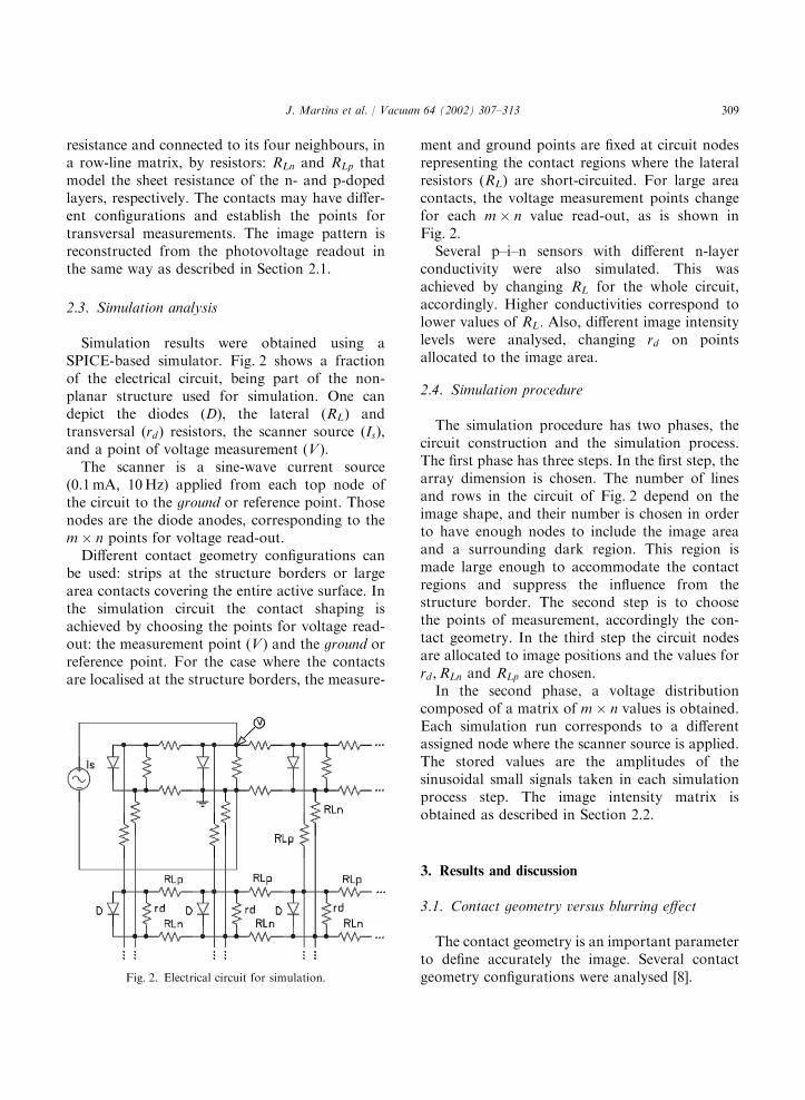
Fig. 3 shows the simulated image intensity of a
rectangle (4� 3) using: (a) strip contacts around
the border and (b) a large area contact covering
the active surface. The values of rd ;RLn and RLpwere kept constant during the simulation process,
with rd=RLn ¼ 10�2: The grey level image repre-
sentation is also depicted.
The results show that contact area and location
play an important role in image representation,
since its location influences the carrier path before
collection [2]. As the contact area increases from
the border strips to cover contacts, a decrease on
the blurring effect is detected. In the configuration
with border strips, the carriers after generation are
diverted in the lateral direction (across RLn;p)towards the contact. The ac component of the
photocurrent decreases in the dark region mainly
near the image border, giving rise to a blurring
effect as shown in Fig. 3a. However, if the contact
area extends all over the active surface, the lateral
path is short-circuited and the carriers are
collected at the generated points. The image
intensity increases and the blurring effect is
minimised (Fig. 3b). Large area contacts all
over the active surface will be used for further
simulations.
3.2. Doped layer resistivities versus spatialresolution
Fig. 4 depicts 3D graphics of the simulated
image intensity and grey levels image representa-
tion outputs from the sensor, obtained under
illumination with two half-circles for two different
ratios: (a) rd=RLn ¼ 10�1 and (b) rd=RLn ¼ 10�2:The rd=RLp ratio was kept constant (10�2) during
the simulation process. For comparison, Fig. 4
shows the experimental results for two sensors
with n-layer conductivities of 2.6� 10�4 and
3.1� 10�5 1/O cm, respectively.
The simulated and experimental results are in
good agreement. The observed difference in both
images depends on the ratio between rd (image
intensity) and RLn (n-layer resistivity) for a
constant value of RLp (p-layer resistivity). As
rd=RLn increases the image intensity smoothes
and it presents some blur at the edges.
Fig. 3. Simulation outputs for: (a) strips border contacts, and (b) large area contacts.
J. Martins et al. / Vacuum 64 (2002) 307–313310
For the sensor having the most resistive layer
(Fig. 4b) the carriers injected near the gap borders by
the ac current source (the scanner) are diverted to the
less resistive path (the image, rd5RLn) and do not
contribute to the ac component of the photocurrent.
If RL;n lowers (Fig. 4a), the border carriers will drift
also in the lateral direction (rdoRLn) toward the
image, increasing the ac component of the current
inside the image and decreasing it outside.
Experimental details support the simulated
results. They show that by using a low conductiv-
ity n-layer (n-SixC1�x : H) a good image represen-
tation is achieved (Fig. 4b), with sharp edges and
almost no blur. However, if the n-layer conductiv-
ity is higher (Fig. 4a) the image intensity repre-
sentation is deteriorated, the edges are blurred and
the wide gap could not be clearly identified. In this
case, some restoring algorithms should be used to
sharpen the edges in blurred image [9].
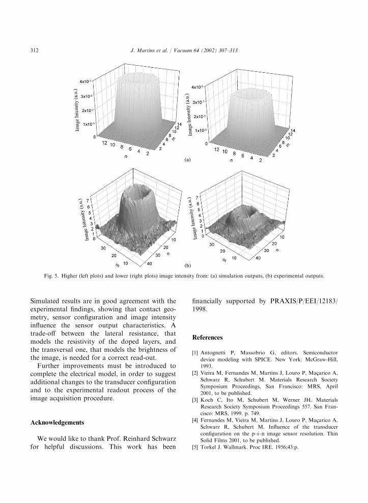
3.3. Image intensity
Fig. 5(a) shows the outputs from the sensor
obtained under a donut illumination for two
different values of rd=RLn : 10�2 (left plots); 10�1
(right plots). RLn and RLp were kept constant
during the simulation process.
For comparison, a 7.5 mm donut having an
inner hole of 2.5 mm diameter was projected onto
the sensor having the most resistive n-layer. The
scanner intensity (FS) was kept constant while the
light source flux (FL) used for mapping the donut
into the sensor was changed. Fig. 5(b) displays the
experimentally acquired images, at FL ¼ 5 mW/
cm2 (left plot) and FL ¼ 0:5 mW/cm2 (right plot)
keeping the scanner flux FS ¼ 2:5 � 10�2 mW/cm2.
A good contrast between the illuminated (low rdvalues) and the dark regions (high rd values) is
observed. As rd decreases, the image intensity
increases. Under full contact collection the carriers
injected by the ac current source flow in the
transversal direction. The potential drop inside the
dark regions is high (high rd) and decreases inside
the illuminated regions, as rd decreases (FL
increases). Again, a good agreement between
simulated (Fig. 5(a)) and experimental (Fig. 5(b))
results is found.
4. Conclusions
A physical model supported by an electrical
simulation was presented. A SPICE based simu-
lator was used to infer the output characteristics.
Fig. 4. Simulation and experimental outputs for: (a) lower n-layer resistivity, (b) higher n-layer resistivity.
J. Martins et al. / Vacuum 64 (2002) 307–313 311
Simulated results are in good agreement with the
experimental findings, showing that contact geo-
metry, sensor configuration and image intensity
influence the sensor output characteristics. A
trade-off between the lateral resistance, that
models the resistivity of the doped layers, and
the transversal one, that models the brightness of
the image, is needed for a correct read-out.
Further improvements must be introduced to
complete the electrical model, in order to suggest
additional changes to the transducer configuration
and to the experimental readout process of the
image acquisition procedure.
Acknowledgements
We would like to thank Prof. Reinhard Schwarz
for helpful discussions. This work has been
financially supported by PRAXIS/P/EEI/12183/
1998.
References
[1] Antognetti P, Massobrio G, editors. Semiconductor
device modeling with SPICE. New York: McGraw-Hill,
1993.
[2] Vieira M, Fernandes M, Martins J, Louro P, Macarico A,
Schwarz R, Schubert M. Materials Research Society
Symposium Proceedings, San Francisco: MRS, April
2001, to be published.
[3] Koch C, Ito M, Schubert M, Werner JH. Materials
Research Society Symposium Proceedings 557. San Fran-
cisco: MRS, 1999. p. 749.
[4] Fernandes M, Vieira M, Martins J, Louro P, Macarico A,
Schwarz R, Schubert M. Influence of the transducer
configuration on the p–i–n image sensor resolution. Thin
Solid Films 2001, to be published.
[5] Torkel J. Wallmark. Proc IRE. 1956;43:p.
Fig. 5. Higher (left plots) and lower (right plots) image intensity from: (a) simulation outputs, (b) experimental outputs.
J. Martins et al. / Vacuum 64 (2002) 307–313312

[6] Wilson J, Hawkes J. Optoelectronics, an introduction.
London: Prentice Hall, 1998.
[7] Vieira M, Morgado E, Macarico A, Koynov S, Schwarz R.
Microcrystalline silicon thin films for optical applications.
Vacuum 1999;52:67–71.
[8] Martins J, Sousa F, Fernandes M, Louro P, Macarico A,
Vieira M. The contact geometry in a 2Dmc-Si.H p–i–n
Imager. Strasbourg: EMRS, 1999.
[9] Sousa F, Martins J, Fernandes M, Macarico A, Schwarz R,
Vieira M. J Non-Cryst Solids 1228;2000:266–9.
J. Martins et al. / Vacuum 64 (2002) 307–313 313