Embed Size (px)
Citation preview
Electrical Overstress – Many Sources; AnySolutions?
Terry Welsher
Dangelmayer Associates
ESD Association
Industry Council on ESDTargets
www.dangelmayer.com
1Copyright 2012, Dangelmayer Assoc. & Semitracks Inc.
Outline
Introduction
EOS and ESD Background
EOS Definitions and Terms
EOS Categorization EOS-like ESD (CBE and CDE)
Power-induced EOS
Factory Mitigation
Design Mitigation
Industry Activities
Conclusions – EOS Survey
2Copyright 2010, Dangelmayer Assoc. & Semitracks Inc.
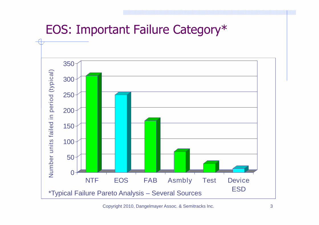
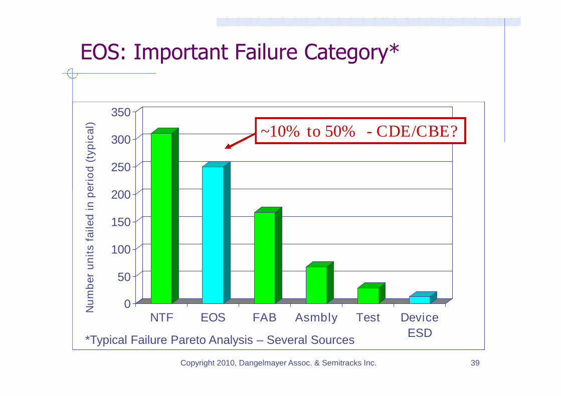
EOS: Important Failure Category*
0
50
100
150
200
250
300
350
NTF EOS FAB Asmbly Test Device
ESD
3Copyright 2010, Dangelmayer Assoc. & Semitracks Inc.
Nu
mb
er
un
its
fail
ed
inp
eri
od
(typ
ica
l)
*Typical Failure Pareto Analysis – Several Sources
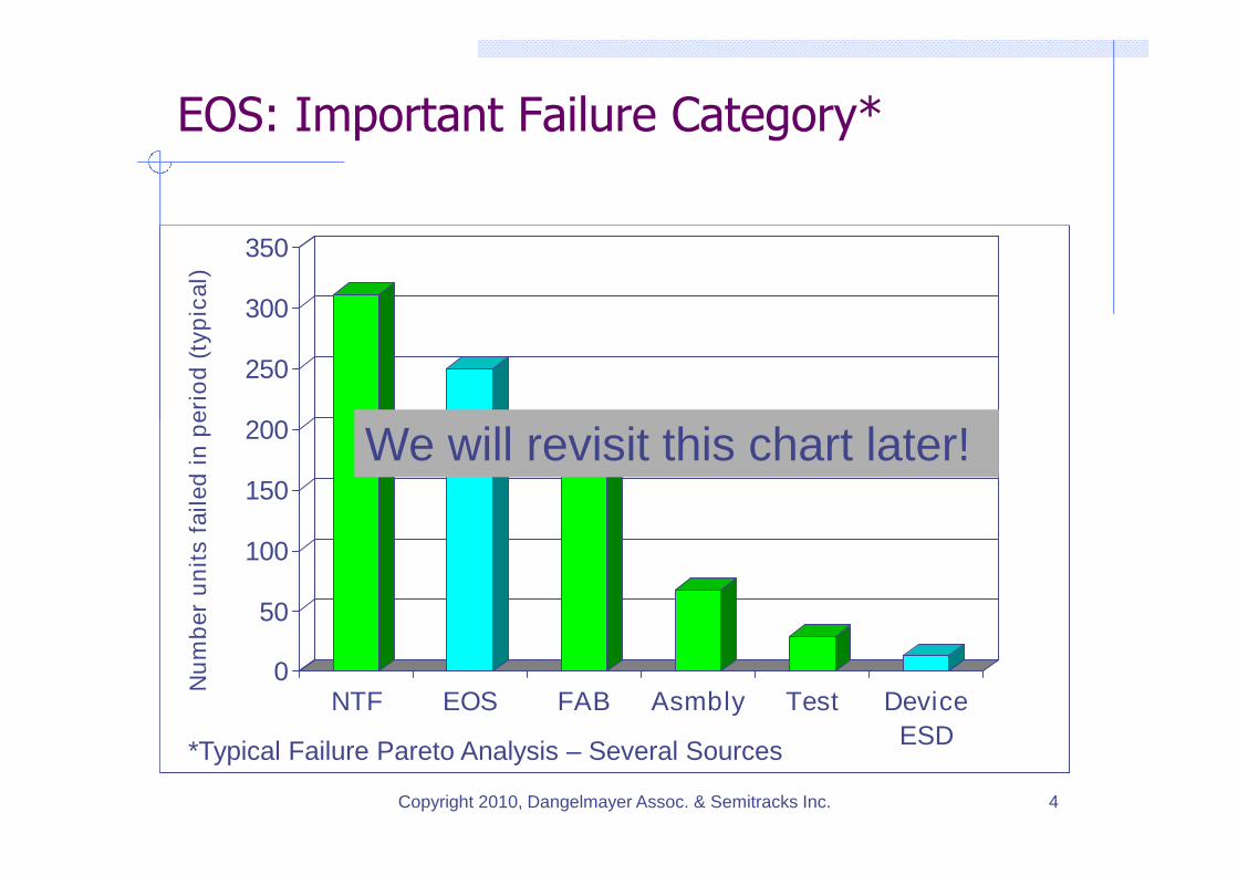
EOS: Important Failure Category*
0
50
100
150
200
250
300
350
NTF EOS FAB Asmbly Test Device
ESD
4Copyright 2010, Dangelmayer Assoc. & Semitracks Inc.
Nu
mb
er
un
its
fail
ed
inp
eri
od
(typ
ica
l)
*Typical Failure Pareto Analysis – Several Sources
We will revisit this chart later!
Costs of EOS/ESD
Many companies agree 25-35% of failuresare EOS/ESD; some say more
High burden for semiconductor and boardassembly
Failure fraction has remained about the sameover many years
Difficult to identify
Finger pointing about who is responsible
Often not systematic
Root cause hard to find
5Copyright 2010, Dangelmayer Assoc. & Semitracks Inc.
EOS Issues/Questions
EOS (by FA diagnoses) is main cause ofelectrical failure of device and systems
Electrical failures sent to FA often returndiagnosis of EOS or EOS/ESD without furtherinformation
More information is needed to find root causeand implement corrective action
Confusion about EOS definition
Much progress has been made on ESD butnot EOS. Why?
6Copyright 2010, Dangelmayer Assoc. & Semitracks Inc.
p7
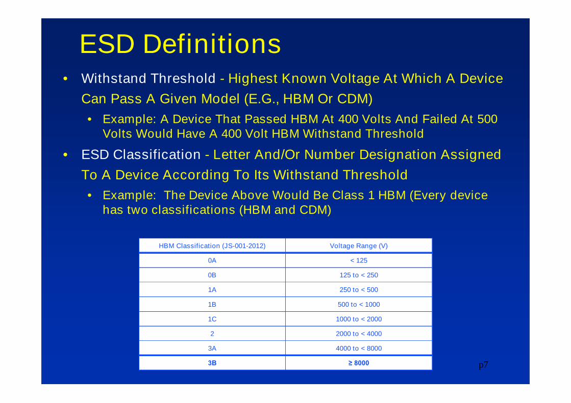
ESD Definitions• Withstand Threshold - Highest Known Voltage At Which A Device
Can Pass A Given Model (E.G., HBM Or CDM)
• Example: A Device That Passed HBM At 400 Volts And Failed At 500Volts Would Have A 400 Volt HBM Withstand Threshold
• ESD Classification - Letter And/Or Number Designation Assigned
To A Device According To Its Withstand Threshold
• Example: The Device Above Would Be Class 1 HBM (Every devicehas two classifications (HBM and CDM)
HBM Classification (JS-001-2012) Voltage Range (V)
0A < 125
0B 125 to < 250
1A 250 to < 500
1B 500 to < 1000
1C 1000 to < 2000
2 2000 to < 4000
3A 4000 to < 8000
3B ≥ 8000
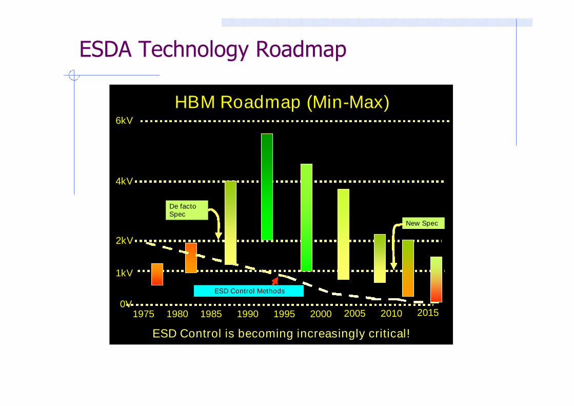
ESDA Technology Roadmap
p8
HBM Roadmap (Min-Max)
1980 1985 1990 1995 2000 2005 2010
4kV
2kV
6kV
ESD Control is becoming increasingly critical!
0V
1kV
ESD Control Methods
20151975
De factoSpec
New Spec

ESDA Technology Roadmap
p9
CDM Roadmap (Min-Max)
1980 1985 1990 1995 2000 2005 2010
500V
ESD Control is becoming increasingly critical!
0V
250V
ESD Control Methods
20151975
New Spec
125V
De factoSpec
OriginalSpecs

Do Device ESD Classifications Apply at theBoard Level? Yes and No
YES – Handling of boards is usually definedby the lowest threshold device on the board
NO – Devices can fail at levels below theirexpected voltage threshold levels whenmounted on PWBs (see CBE discussion later)
10Copyright 2010, Dangelmayer Assoc. & Semitracks Inc.
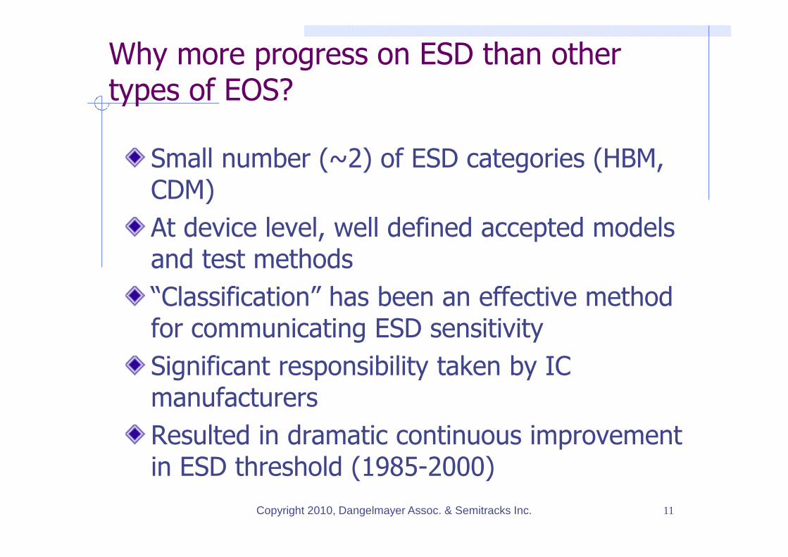
Why more progress on ESD than othertypes of EOS?
Small number (~2) of ESD categories (HBM,CDM)
At device level, well defined accepted modelsand test methods
“Classification” has been an effective methodfor communicating ESD sensitivity
Significant responsibility taken by ICmanufacturers
Resulted in dramatic continuous improvementin ESD threshold (1985-2000)
11Copyright 2010, Dangelmayer Assoc. & Semitracks Inc.

Early EOS Standard
IEC60134 (January 1961) - Rating systemsfor electronic tubes and valves and analogoussemiconductor devices
Scope: This recommendation applies to ratingsystems in use for electronic tubes and valves andsemiconductor devices.
Definitions of rating, rating system, absolutemaximum rating system, design maximum ratingsystem, design centre rating system
Copyright 2011, Dangelmayer Assoc. 12
13
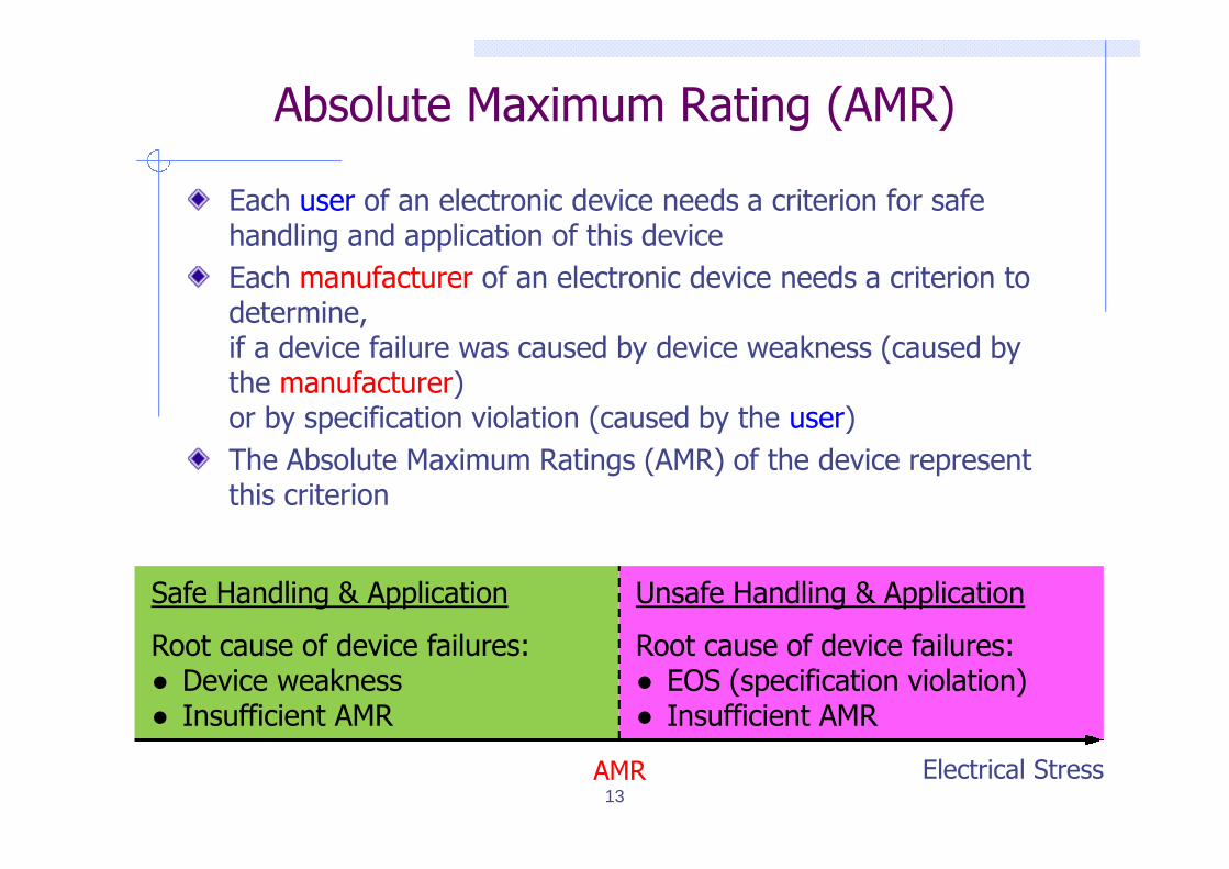
Absolute Maximum Rating (AMR)
Each user of an electronic device needs a criterion for safehandling and application of this device
Each manufacturer of an electronic device needs a criterion todetermine,if a device failure was caused by device weakness (caused bythe manufacturer)or by specification violation (caused by the user)
The Absolute Maximum Ratings (AMR) of the device representthis criterion
Unsafe Handling & Application
Root cause of device failures:● EOS (specification violation)● Insufficient AMR
Safe Handling & Application
Root cause of device failures:● Device weakness● Insufficient AMR
Electrical StressAMR
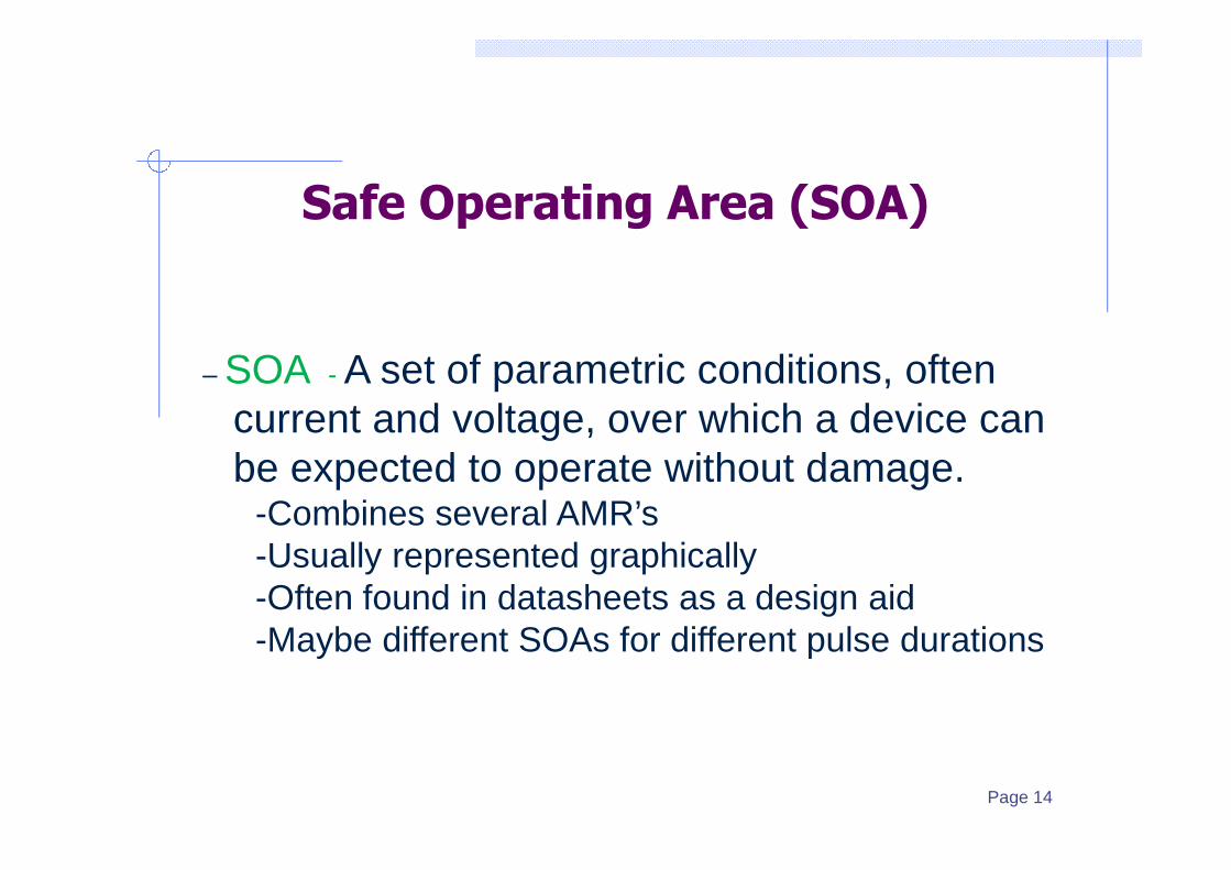
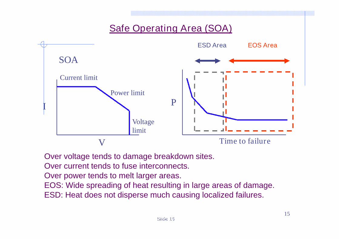
Safe Operating Area (SOA)
Page 14
– SOA - A set of parametric conditions, oftencurrent and voltage, over which a device canbe expected to operate without damage.
-Combines several AMR’s-Usually represented graphically-Often found in datasheets as a design aid-Maybe different SOAs for different pulse durations
Slide 1515
Safe Operating Area (SOA)
Over voltage tends to damage breakdown sites.Over current tends to fuse interconnects.Over power tends to melt larger areas.EOS: Wide spreading of heat resulting in large areas of damage.ESD: Heat does not disperse much causing localized failures.
P
Time to failure
EOS AreaESD Area
SOA
I
V
Current limit
Voltagelimit
Power limit
causing localized failures.
age tends to damage breakdown sites.Over current tends to fuse interconnects.Over power tends to melt larger areas.EOS: Wide spreading of heat resulting in large areas of damage.
Over voltage tends to damage breakdown sites.Over current tends to fuse interconnects.Over power tends to melt larger areas.EOS: Wide spreading of heat resulting in large areas of damage.ESD: Heat does not disperse much causing localized failures.
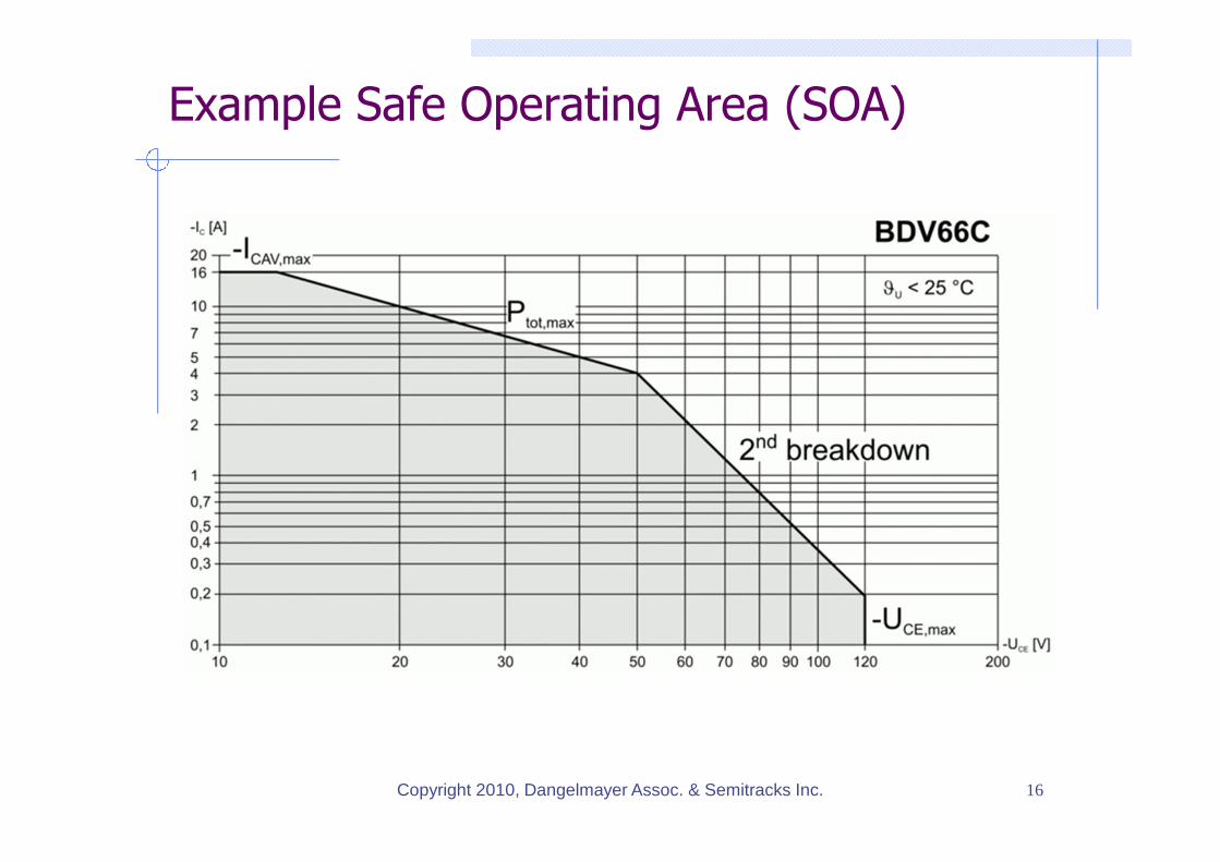
Example Safe Operating Area (SOA)
Copyright 2010, Dangelmayer Assoc. & Semitracks Inc. 16
Page 17
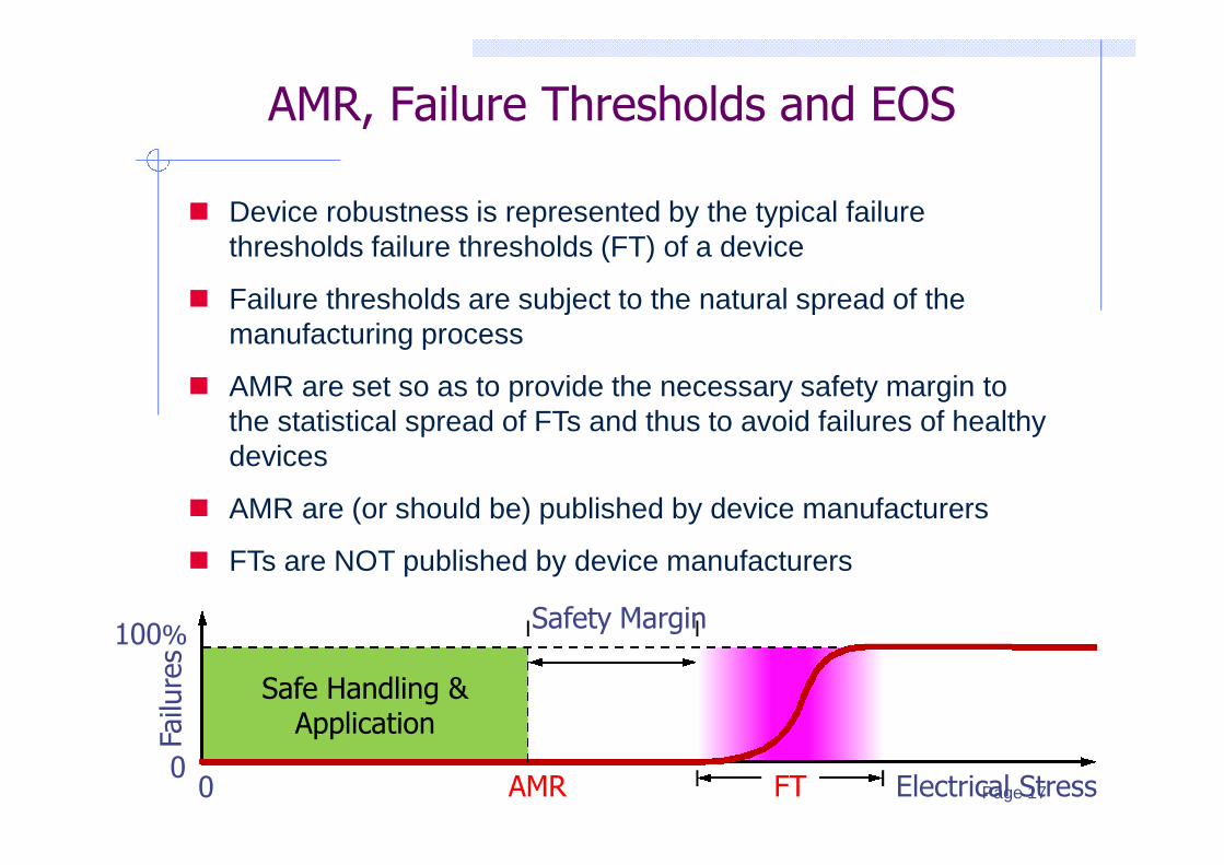
AMR, Failure Thresholds and EOS
Device robustness is represented by the typical failurethresholds failure thresholds (FT) of a device
Failure thresholds are subject to the natural spread of themanufacturing process
AMR are set so as to provide the necessary safety margin tothe statistical spread of FTs and thus to avoid failures of healthydevices
AMR are (or should be) published by device manufacturers
FTs are NOT published by device manufacturers
Safe Handling &Application
Electrical Stress
Failu
res
100%
00 FTAMR
Safety Margin
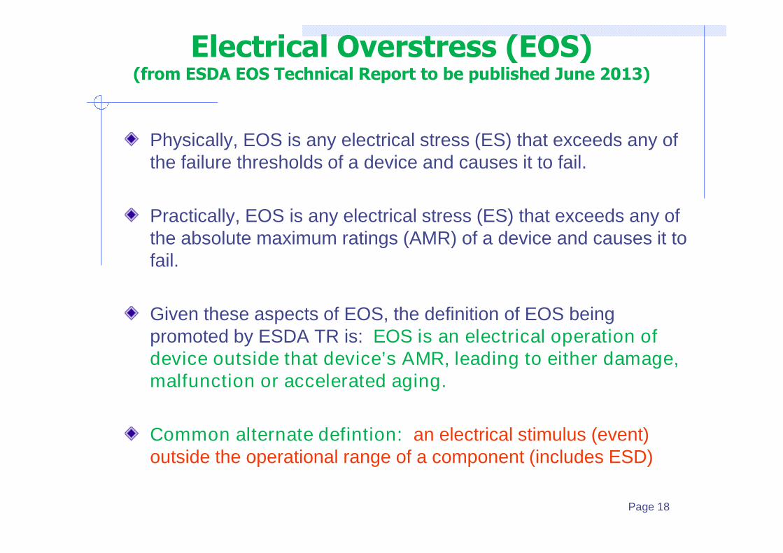
Physically, EOS is any electrical stress (ES) that exceeds any ofthe failure thresholds of a device and causes it to fail.
Practically, EOS is any electrical stress (ES) that exceeds any ofthe absolute maximum ratings (AMR) of a device and causes it tofail.
Given these aspects of EOS, the definition of EOS beingpromoted by ESDA TR is: EOS is an electrical operation ofdevice outside that device’s AMR, leading to either damage,malfunction or accelerated aging.
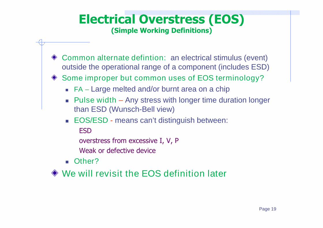
Common alternate defintion: an electrical stimulus (event)outside the operational range of a component (includes ESD)
Page 18
Electrical Overstress (EOS)(from ESDA EOS Technical Report to be published June 2013)
Common alternate defintion: an electrical stimulus (event)outside the operational range of a component (includes ESD)
Some improper but common uses of EOS terminology?
FA – Large melted and/or burnt area on a chip
Pulse width – Any stress with longer time duration longerthan ESD (Wunsch-Bell view)
EOS/ESD - means can’t distinguish between:
ESD
overstress from excessive I, V, P
Weak or defective device
Other?
We will revisit the EOS definition later
Page 19
Electrical Overstress (EOS)(Simple Working Definitions)
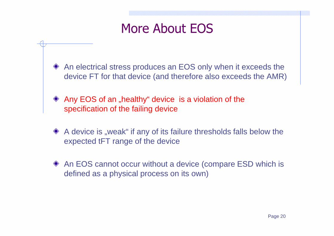
An electrical stress produces an EOS only when it exceeds thedevice FT for that device (and therefore also exceeds the AMR)
Any EOS of an „healthy“ device is a violation of thespecification of the failing device
A device is „weak“ if any of its failure thresholds falls below theexpected tFT range of the device
An EOS cannot occur without a device (compare ESD which isdefined as a physical process on its own)
Page 20
More About EOS
How do we categorize EOS?
By Stress Type?
By Failure Signature and Physical Damage?
By Root Cause?
By Failure Mechanism?
By Pulse Waveform Characteristics?
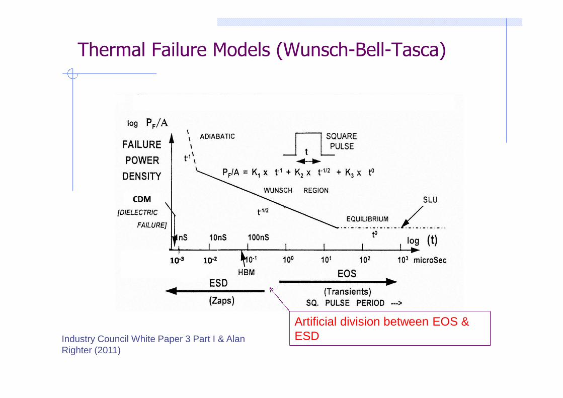
Thermal Failure Models (Wunsch-Bell-Tasca)
Industry Council White Paper 3 Part I & AlanRighter (2011)
Artificial division between EOS &ESD
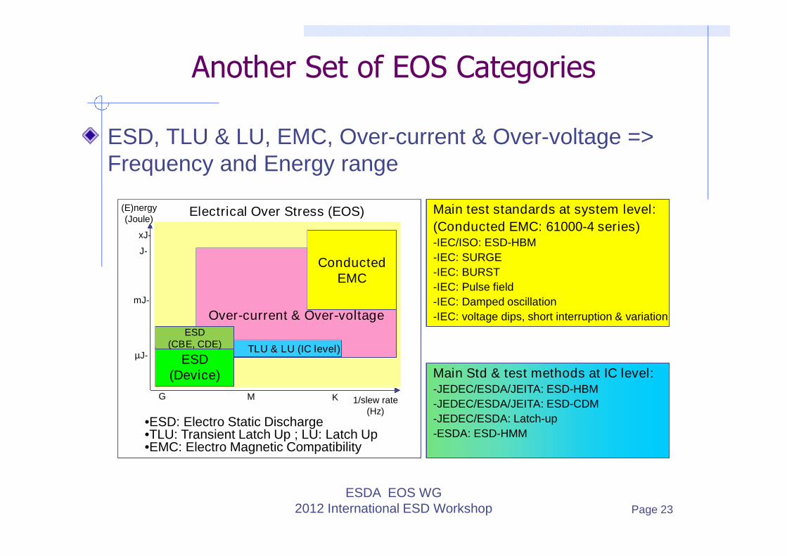
Another Set of EOS Categories
ESD, TLU & LU, EMC, Over-current & Over-voltage =>Frequency and Energy range
Page 23
ESDA EOS WG2012 International ESD Workshop
(E)nergy(Joule)
1/slew rate(Hz)
µJ-
mJ-
xJ-
Electrical Over Stress (EOS)
Over-current & Over-voltage
G M K
TLU & LU (IC level)ESD
(Device)
ConductedEMC
J-
•ESD: Electro Static Discharge•TLU: Transient Latch Up ; LU: Latch Up•EMC: Electro Magnetic Compatibility
Main Std & test methods at IC level:-JEDEC/ESDA/JEITA: ESD-HBM
-JEDEC/ESDA/JEITA: ESD-CDM
-JEDEC/ESDA: Latch-up
-ESDA: ESD-HMM
Main test standards at system level:
(Conducted EMC: 61000-4 series)-IEC/ISO: ESD-HBM
-IEC: SURGE
-IEC: BURST
-IEC: Pulse field
-IEC: Damped oscillation
-IEC: voltage dips, short interruption & variation
ESD(CBE, CDE)

Causes of EOS Events
NOTE: EOS is not a root
cause but aconsequence
Kaschani & Gaertner, 2011 EOS/ESDSymposium and ESDA EOS TR
RF /
EMP
Spec
violations
Mis-
insertion
EOS
Misorientation /misalignment
Hot plugging
Assembly
Misalignment
Hot plugging
Open / shortedsupply lines
Othercomponents
Overheating Intermittentcontacts
Power supplysequencing
Accidentalpower fails
Misapplication
PCB design
Lack of filters Lack ofshielding
Noise
Hard switching
Lack of filters
Surge
currents
Poor electrical isolation
Switching of capacitors
Fast voltage
transients
Power up / down
Inductive switching
EMI
Slow voltage
transients
System
Design
Heat dissipation
Software
Testing
Instable /incomplete tests
Hot switching /plugging
SystemLevel
ComponentLevel
HBMCDM
SL-HBM(IEC/ISO)
CBE
CDE
ESD
Saturationof inductors
Others
Others
Others
Misinterpretationof standards
Testerartifacts
Mishandling
Misapplicationof testers
Charged-Board Event – ESD that “lookslike” EOS
Copyright 2010, Dangelmayer Assoc. & Semitracks Inc. 25
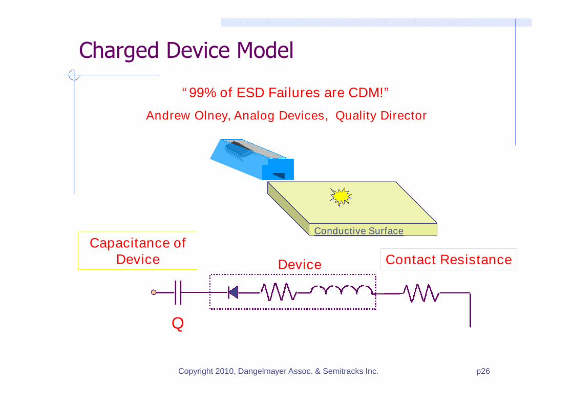
Charged Device Model
Conductive Surface
Device Contact ResistanceCapacitance of
Device
Charge“Flow”
Q
Ground
“99% of ESD Failures are CDM!”
Andrew Olney, Analog Devices, Quality Director
p26Copyright 2010, Dangelmayer Assoc. & Semitracks Inc.
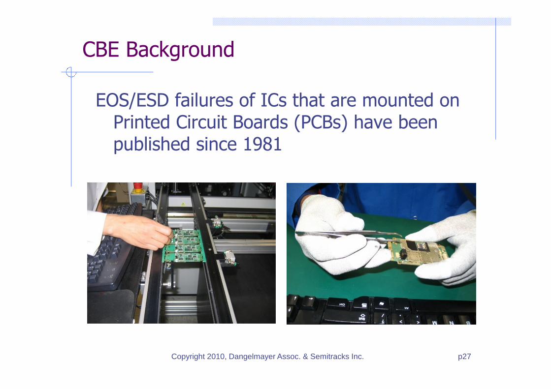
CBE Background
EOS/ESD failures of ICs that are mounted onPrinted Circuit Boards (PCBs) have beenpublished since 1981
*Sometimes called CBM (model). We use CBE (event) toemphasize that there is no standard simulation method p27Copyright 2010, Dangelmayer Assoc. & Semitracks Inc.
Copyright © 2003Dangelmayer Associates
28
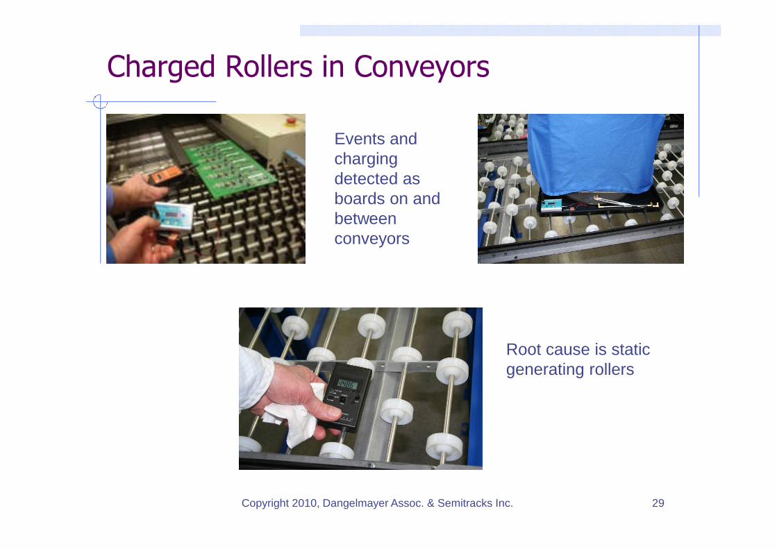
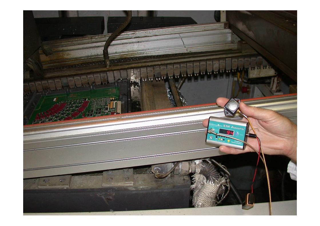
Charged Rollers in Conveyors
Copyright 2010, Dangelmayer Assoc. & Semitracks Inc. 29
Events andchargingdetected asboards on andbetweenconveyors
Root cause is staticgenerating rollers
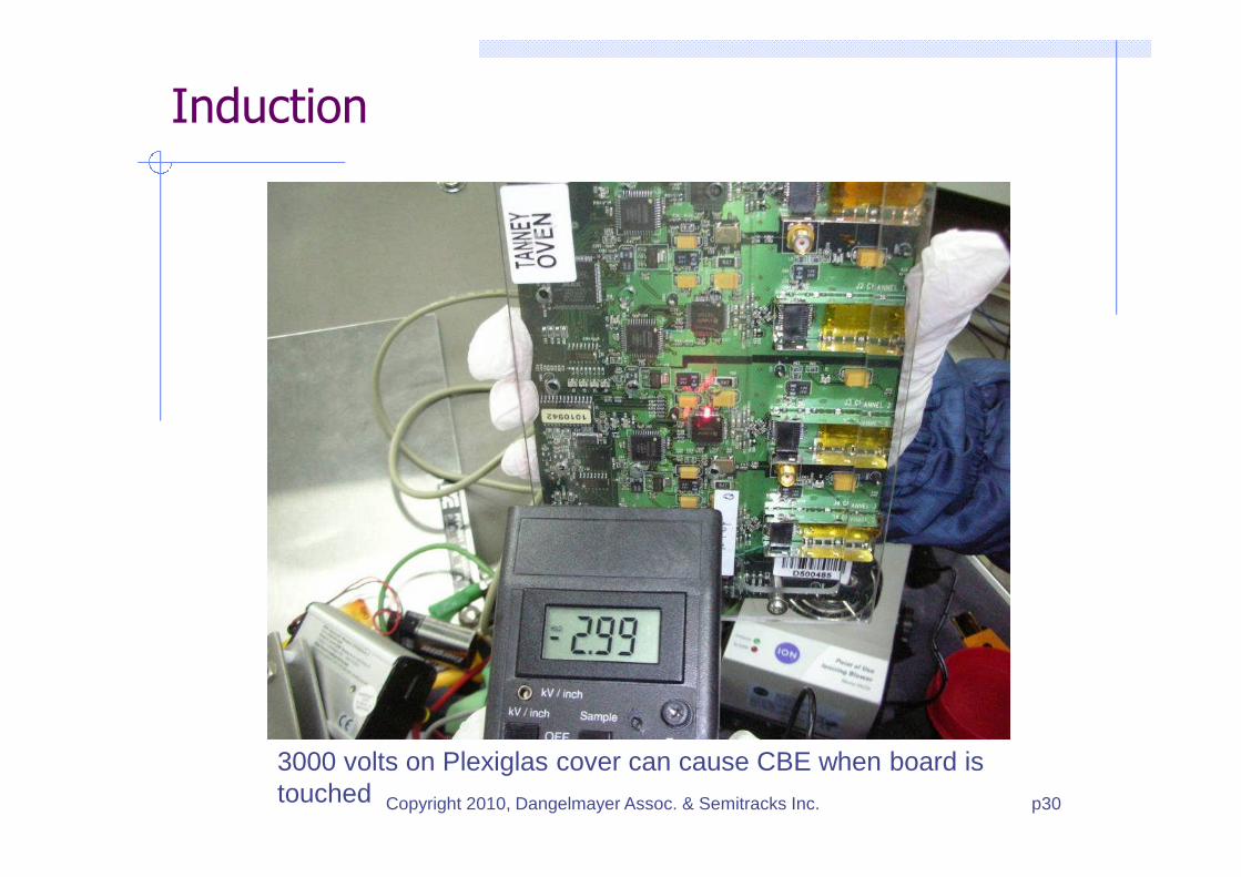
Induction
p30Copyright 2010, Dangelmayer Assoc. & Semitracks Inc.
3000 volts on Plexiglas cover can cause CBE when board istouched
Copyright © 2012 Dangelmayer Associates
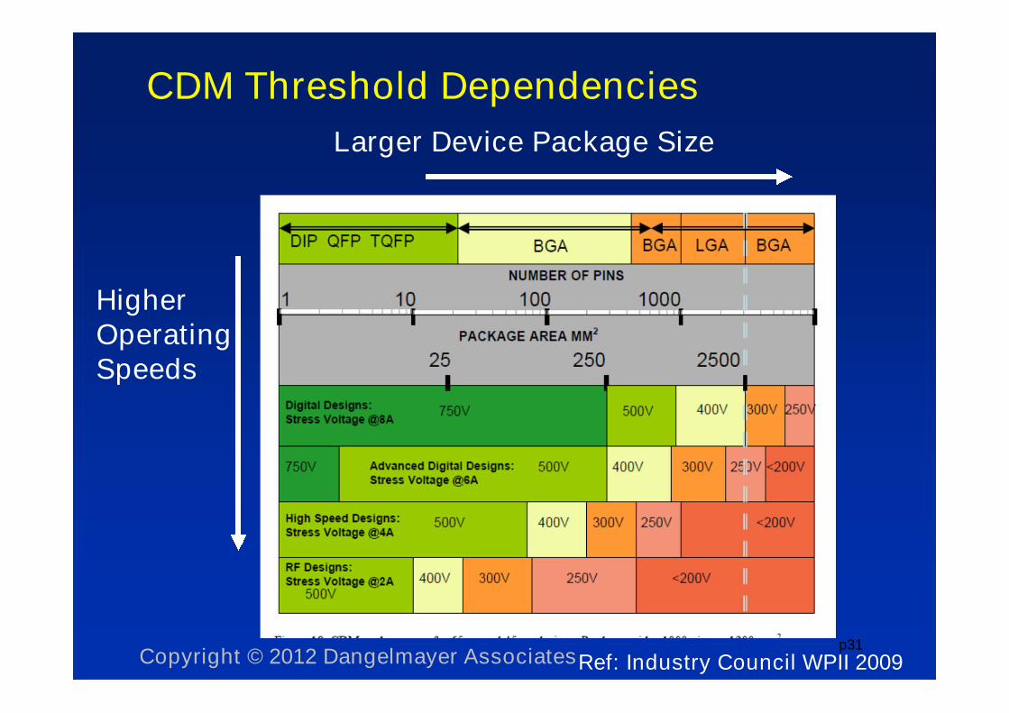
CDM Threshold Dependencies
Ref: Industry Council WPII 2009
Larger Device Package Size
HigherOperatingSpeeds
p31

Copyright © 2012 Dangelmayer Associates
CDM Threshold Dependencies
Ref: Industry Council WPII 2009
Larger Device Package Size
HigherOperatingSpeeds
p32
CBE
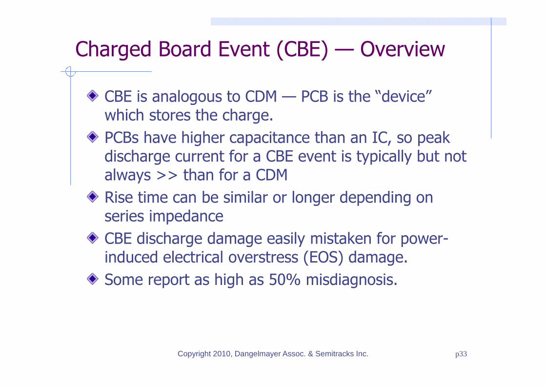
Charged Board Event (CBE) — Overview
CBE is analogous to CDM — PCB is the “device”which stores the charge.
PCBs have higher capacitance than an IC, so peakdischarge current for a CBE event is typically but notalways >> than for a CDM
Rise time can be similar or longer depending onseries impedance
CBE discharge damage easily mistaken for power-induced electrical overstress (EOS) damage.
Some report as high as 50% misdiagnosis.
p33Copyright 2010, Dangelmayer Assoc. & Semitracks Inc.
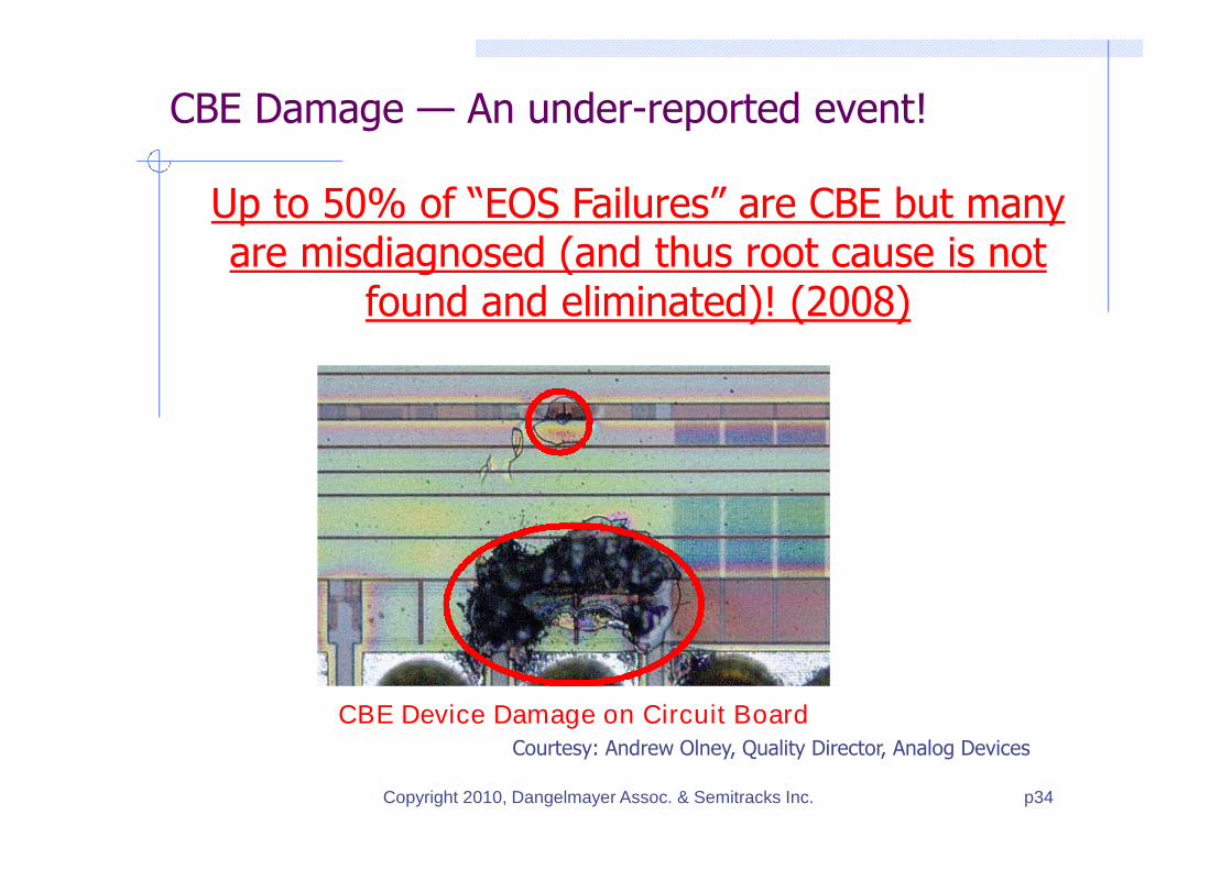
Courtesy: Andrew Olney, Quality Director, Analog Devices
Up to 50% of “EOS Failures” are CBE but manyare misdiagnosed (and thus root cause is not
found and eliminated)! (2008)
CBE Device Damage on Circuit Board
CBE Damage — An under-reported event!
p34Copyright 2010, Dangelmayer Assoc. & Semitracks Inc.
for DSP with a 250V Charge Voltage
-2
0
2
4
6
8
100.0
0
0.2
5
0.5
0
0.7
5
1.0
0
1.2
5
1.5
0
Time (nanoseconds)
Pe
ak
Cu
rre
nt
(Am
ps
) GND test pad FICBM
GND pin FICDM
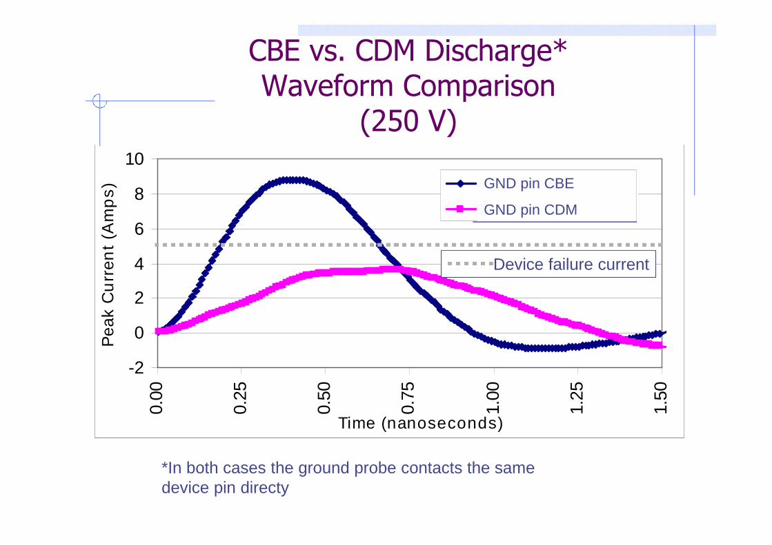
CBE vs. CDM Discharge*Waveform Comparison
(250 V)
Courtesy: Andrew Olney, Quality Director, Analog Devices
Device failure current
GND pin CBE
GND pin CDM
*In both cases the ground probe contacts the samedevice pin directy
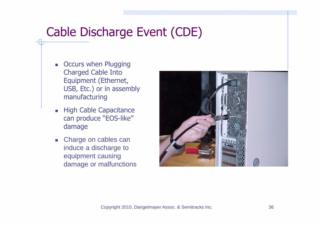
Cable Discharge Event (CDE)
36Copyright 2010, Dangelmayer Assoc. & Semitracks Inc.
Occurs when PluggingCharged Cable IntoEquipment (Ethernet,USB, Etc.) or in assemblymanufacturing
High Cable Capacitancecan produce “EOS-like”damage
Charge on cables caninduce a discharge toequipment causingdamage or malfunctions
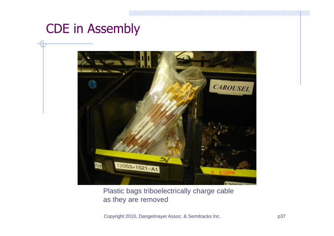
CDE in Assembly
p37Copyright 2010, Dangelmayer Assoc. & Semitracks Inc.
Plastic bags triboelectrically charge cableas they are removed
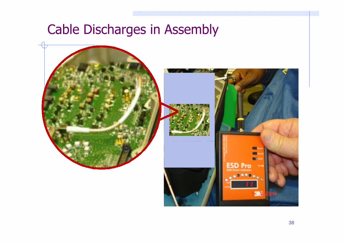
Cable Discharges in Assembly
38
EOS: Important Failure Category*
0
50
100
150
200
250
300
350
NTF EOS FAB Asmbly Test Device
ESD
~10% to 50% - CDE/CBE?
39Copyright 2010, Dangelmayer Assoc. & Semitracks Inc.
Nu
mb
er
un
its
fail
ed
inp
eri
od
(typ
ica
l)
*Typical Failure Pareto Analysis – Several Sources
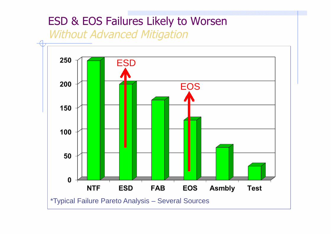
ESD & EOS Failures Likely to WorsenWithout Advanced Mitigation
EOS
ESD
*Typical Failure Pareto Analysis – Several Sources
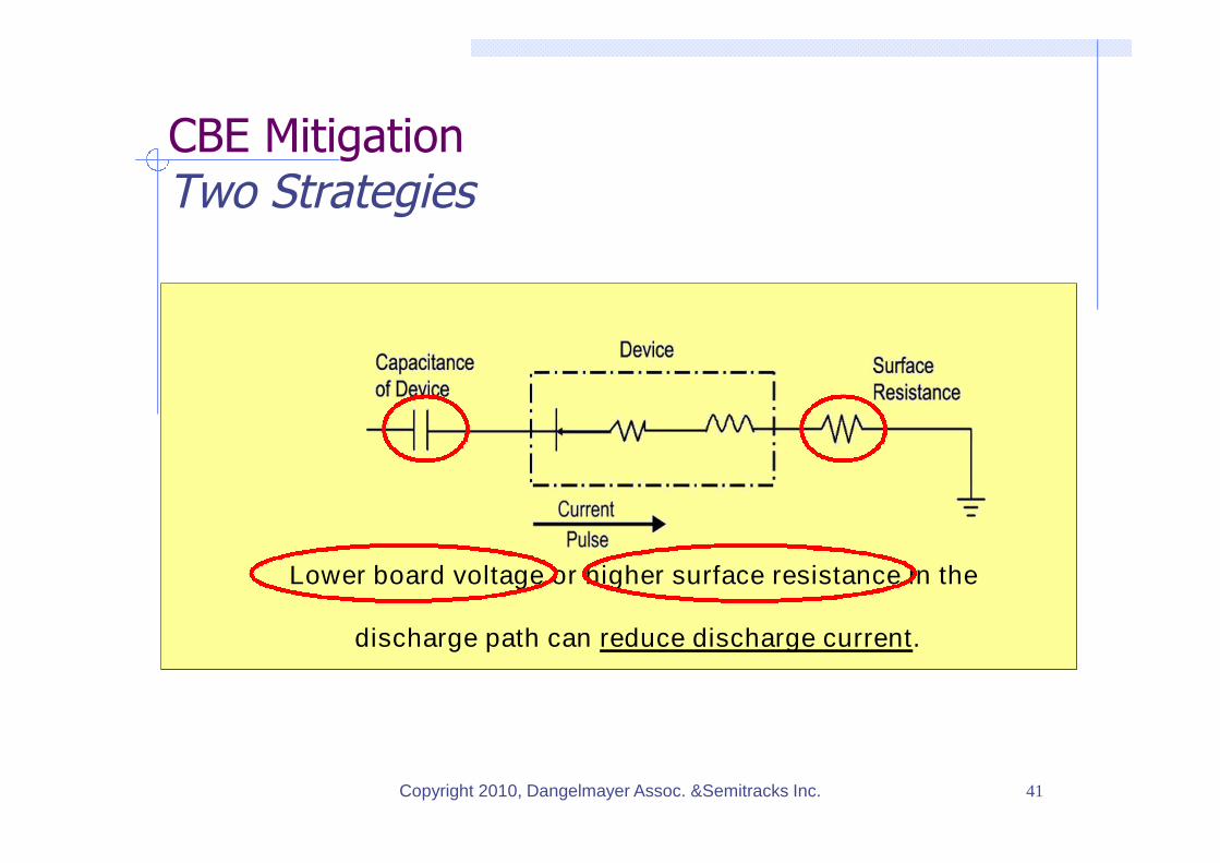
CBE MitigationTwo Strategies
Lower board voltage or higher surface resistance in the
discharge path can reduce discharge current.
41Copyright 2010, Dangelmayer Assoc. &Semitracks Inc.
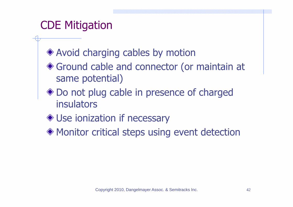
CDE Mitigation
Avoid charging cables by motion
Ground cable and connector (or maintain atsame potential)
Do not plug cable in presence of chargedinsulators
Use ionization if necessary
Monitor critical steps using event detection
Copyright 2010, Dangelmayer Assoc. & Semitracks Inc. 42
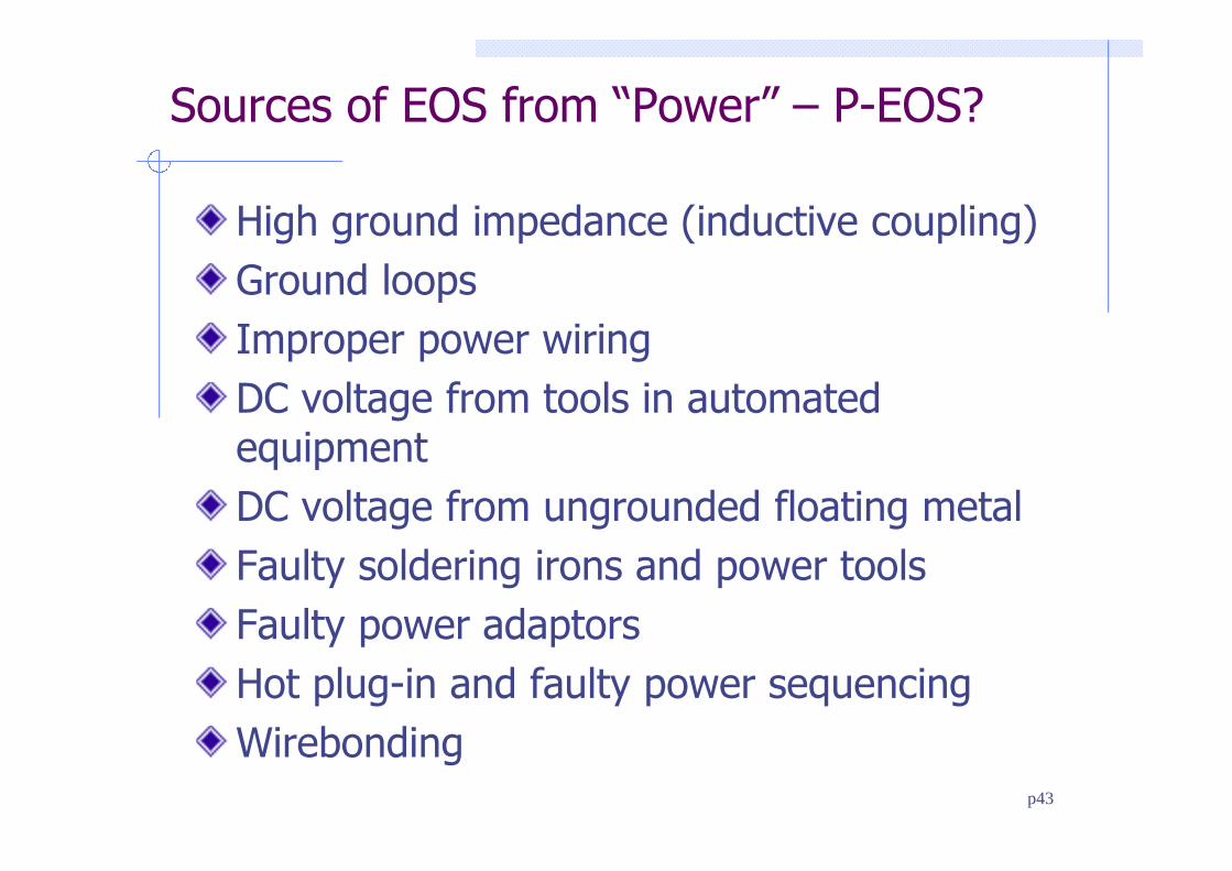
Sources of EOS from “Power” – P-EOS?
High ground impedance (inductive coupling)
Ground loops
Improper power wiring
DC voltage from tools in automatedequipment
DC voltage from ungrounded floating metal
Faulty soldering irons and power tools
Faulty power adaptors
Hot plug-in and faulty power sequencing
Wirebondingp43
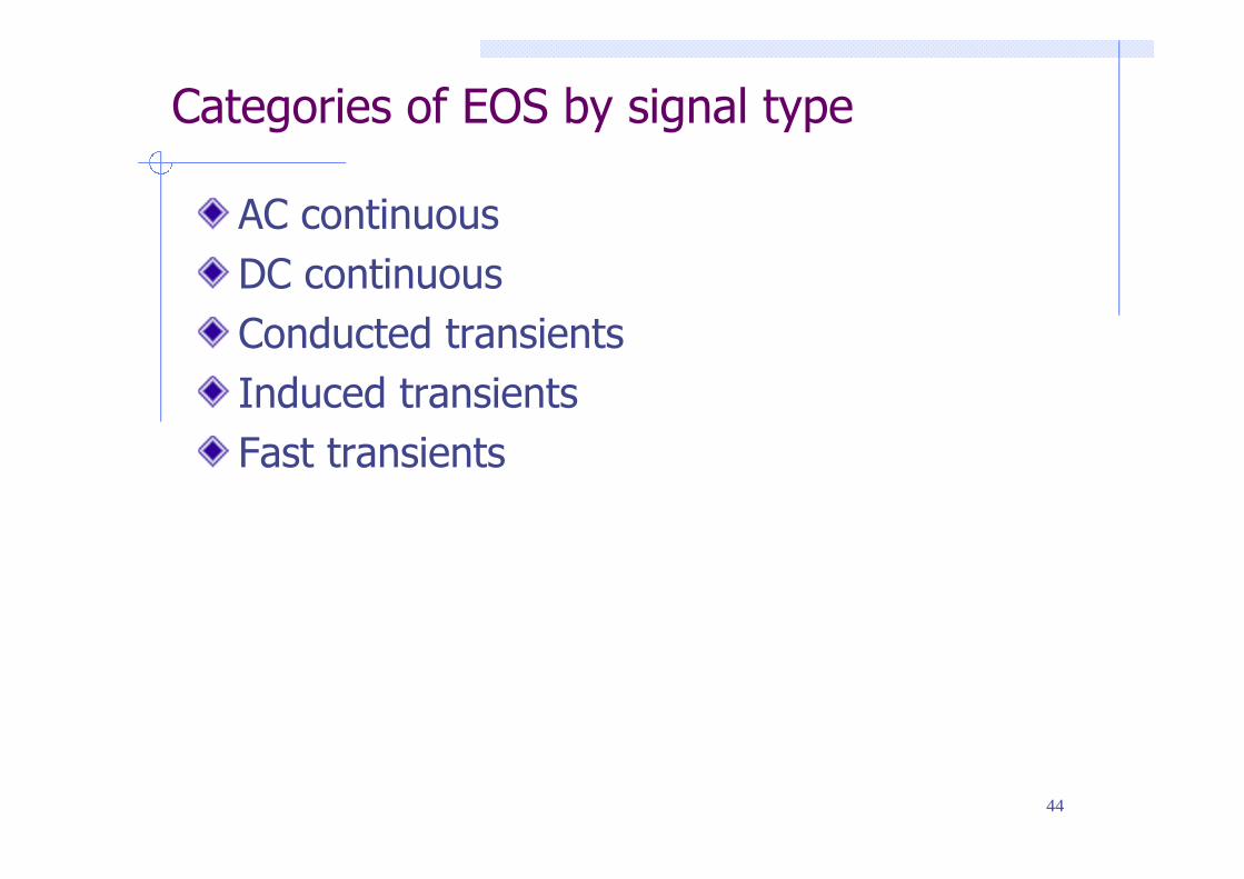
Categories of EOS by signal type
AC continuous
DC continuous
Conducted transients
Induced transients
Fast transients
44
Sources of EOS in Manufacturing and Test
Copyright 2010, Dangelmayer Assoc. & Semitracks Inc. 45
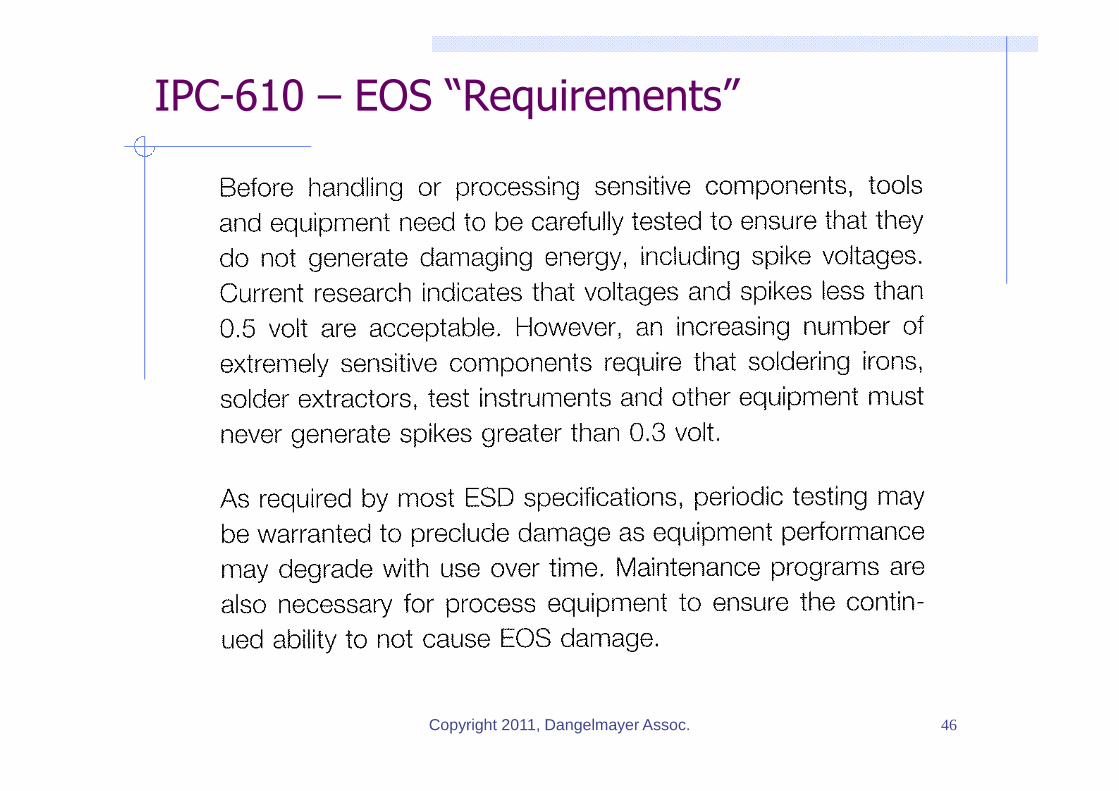
IPC-610 – EOS “Requirements”
Copyright 2011, Dangelmayer Assoc. 46
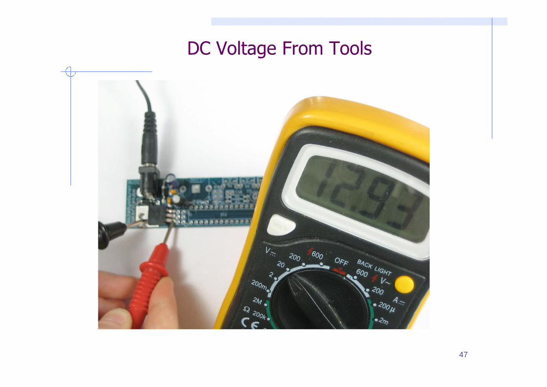
DC Voltage From Tools
47
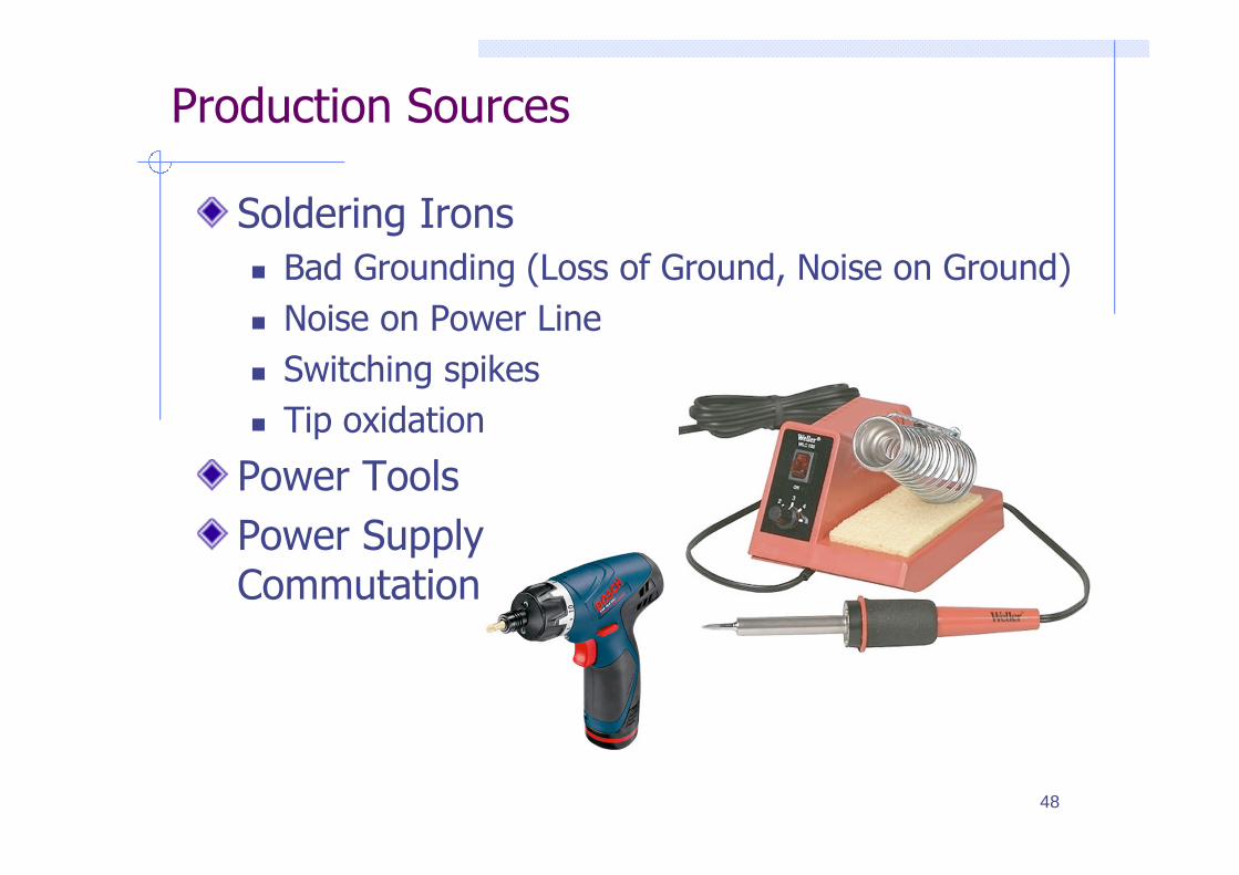
Production Sources
Soldering Irons
Bad Grounding (Loss of Ground, Noise on Ground)
Noise on Power Line
Switching spikes
Tip oxidation
Power Tools
Power SupplyCommutation
48

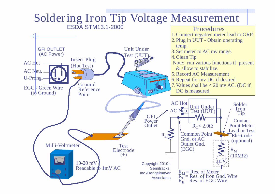
ESD Association STM13.1-2000
Electrical Soldering/Desoldering Hand Tools
Tests:• Resistance
• Voltage
• Current
Provides electric soldering/desoldering hand tool test methods formeasuring electrical leakage and tip to ground reference pointresistance
49
Copyright 2010 -Semitracks,
Inc./DangelmayerAssociates
Soldering Iron Tip Voltage Measurement
GFI OUTLET(AC Power)
Insert Plug(Hot Test)
Unit UnderTest (UUT)
GroundReferencePoint
Milli-Voltmeter TestElectrode
(+)
+-
10-20 mVReadable to 1mV AC
AC Hot
AC Neu.
EGC - Green Wire(to Ground)
U-Prong.
1.Connect negative meter lead to GRP.2.Plug in UUT - Obtain operating
temp.3.Set meter to AC mv range.4.Clean TipNote: run various functions if present
& allow to stabilize.5.Record AC Measurement6.Repeat for mv DC if desired.7.Values shall be < 20 mv AC. (DC if
DC is measured.
Procedures
mV
SolderIronTip
Unit UnderTest (UUT)
RM
(10M)
ContactPoint MeterLead or Test
Electrode(optional)
Common PointGnd. or ACOutlet Gnd.(EGC)
RG< 2.0
AC Hot
AC Neu.GFI
PowerOutlet
RM = Res. of MeterRG = Res. of Iron Gnd. WireRE = Res. of EGC Wire
RE
ESDA STM13.1-2000

Faulty Power Receptacles
51
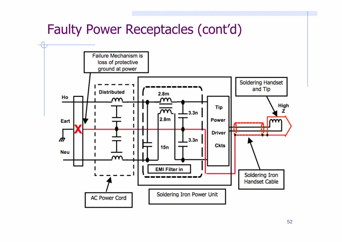
Faulty Power Receptacles (cont’d)
52
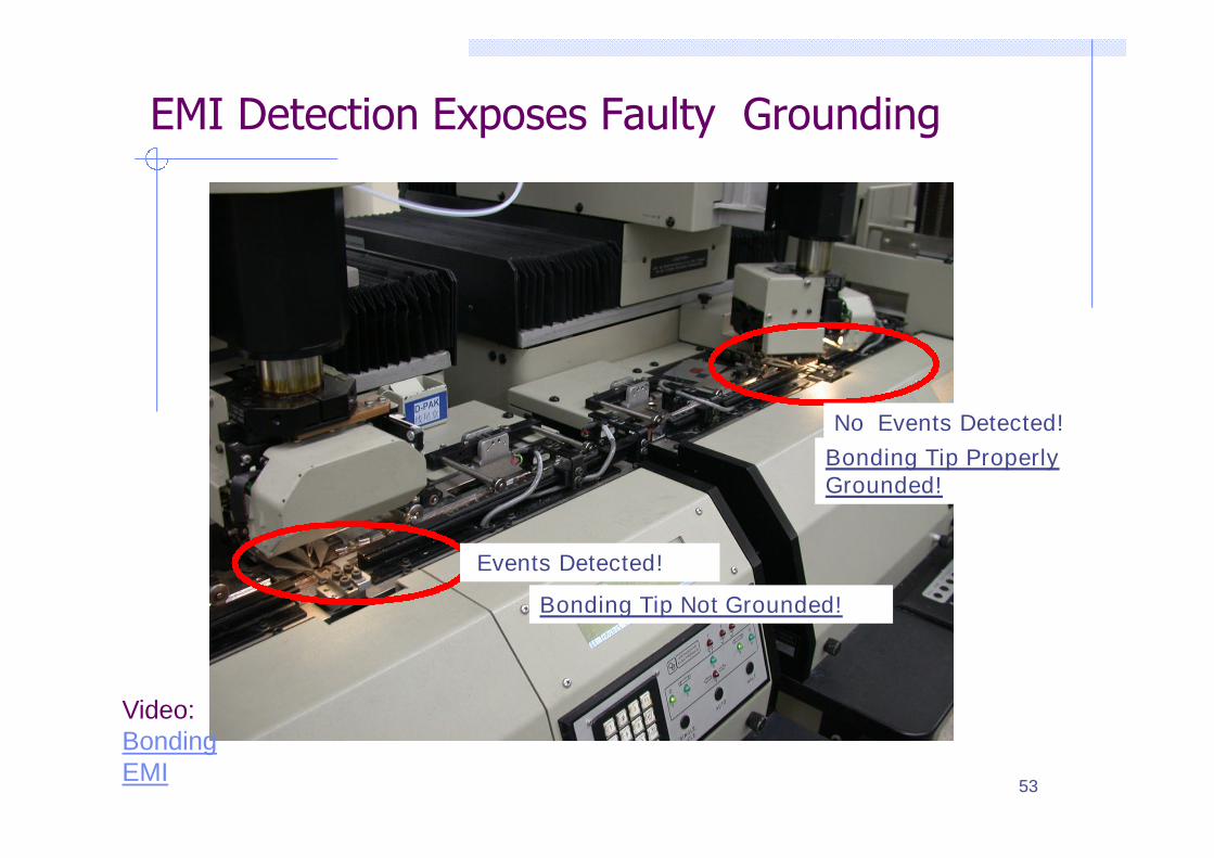
EMI Detection Exposes Faulty Grounding
No Events Detected!
Events Detected!
Bonding Tip Not Grounded!
Bonding Tip ProperlyGrounded!
Video:BondingEMI
53
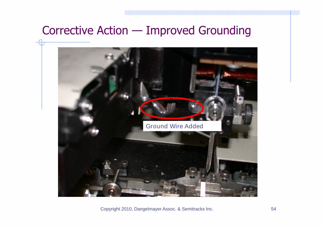
Corrective Action — Improved Grounding
Ground Wire Added
54Copyright 2010, Dangelmayer Assoc. & Semitracks Inc.
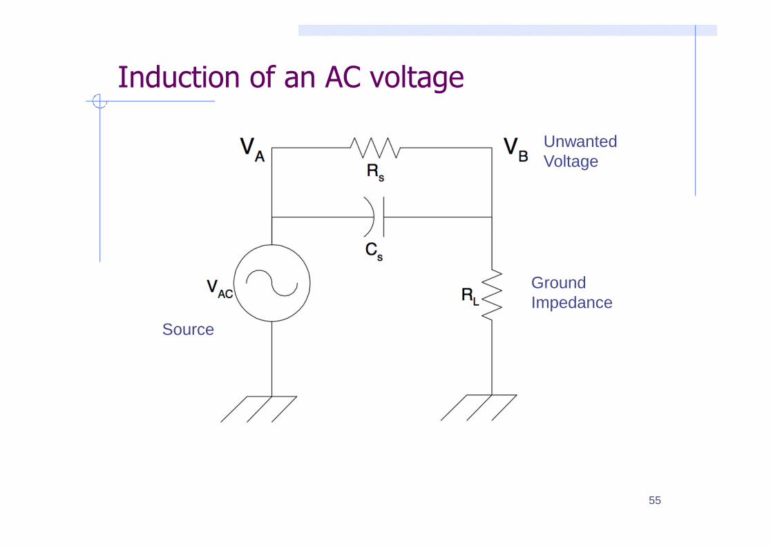
Induction of an AC voltage
55
GroundImpedance
UnwantedVoltage
Source
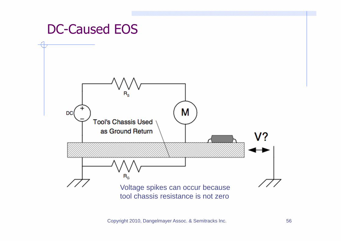
DC-Caused EOS
56Copyright 2010, Dangelmayer Assoc. & Semitracks Inc.
Voltage spikes can occur becausetool chassis resistance is not zero
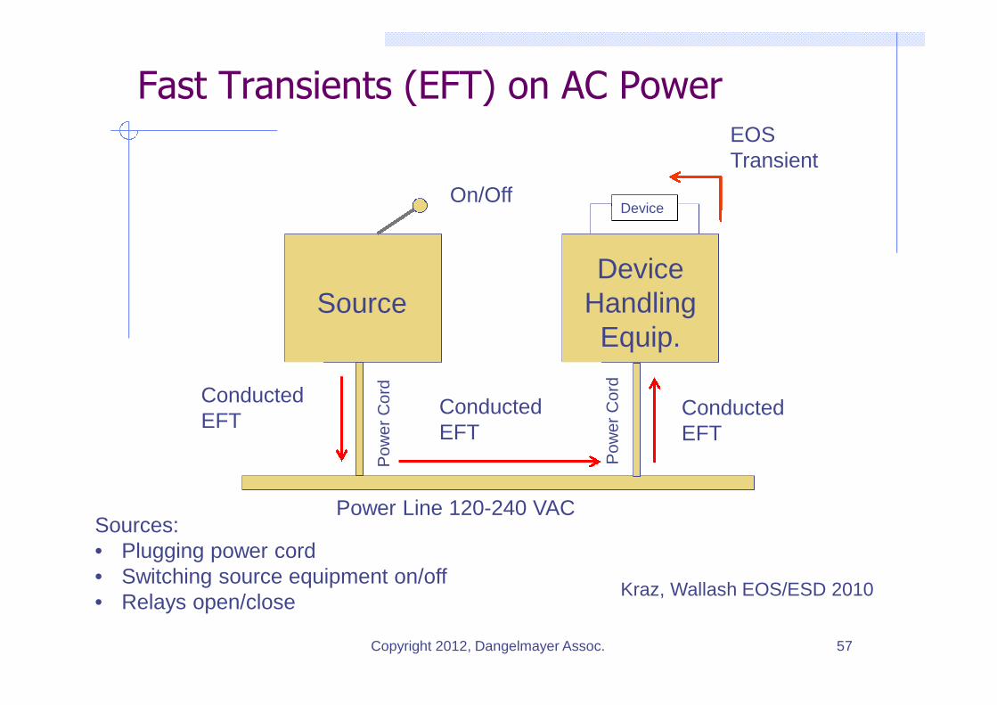
Fast Transients (EFT) on AC Power
57Copyright 2012, Dangelmayer Assoc.
EOSTransient
Power Line 120-240 VAC
Source
On/Off
DeviceHandlingEquip.
Device
ConductedEFT
ConductedEFT
ConductedEFT
Pow
er
Cord
Pow
er
Cord
Sources:• Plugging power cord• Switching source equipment on/off• Relays open/close
Kraz, Wallash EOS/ESD 2010
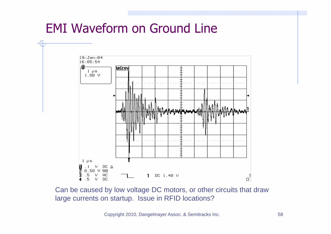
EMI Waveform on Ground Line
58Copyright 2010, Dangelmayer Assoc. & Semitracks Inc.
Can be caused by low voltage DC motors, or other circuits that drawlarge currents on startup. Issue in RFID locations?
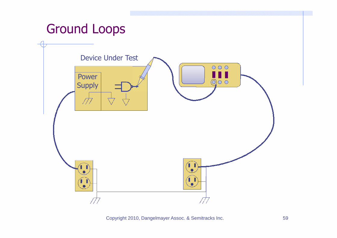
Ground Loops
Device Under Test
PowerSupply
59Copyright 2010, Dangelmayer Assoc. & Semitracks Inc.
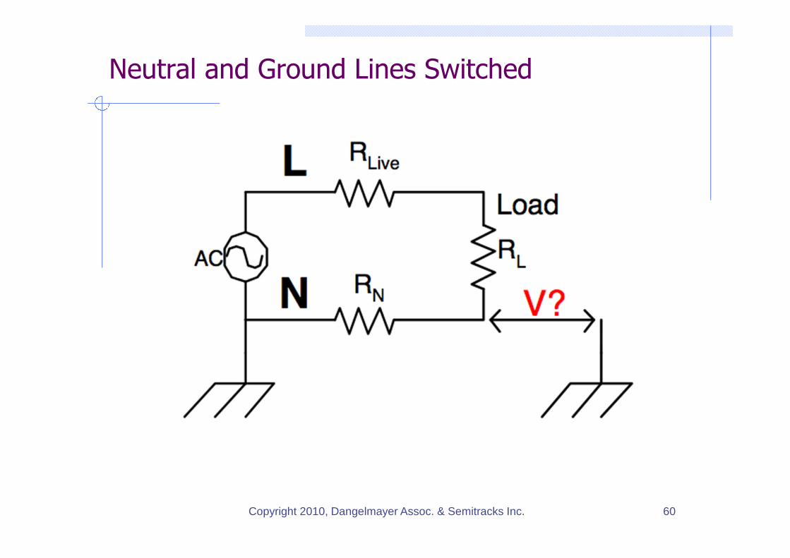
Neutral and Ground Lines Switched
60Copyright 2010, Dangelmayer Assoc. & Semitracks Inc.
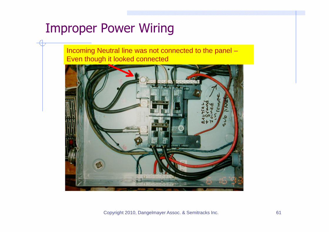
Improper Power Wiring
61Copyright 2010, Dangelmayer Assoc. & Semitracks Inc.
Incoming Neutral line was not connected to the panel –Even though it looked connected
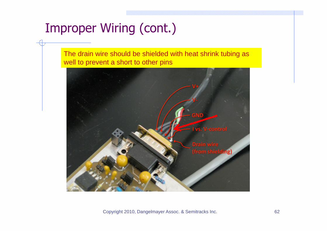
Improper Wiring (cont.)
62Copyright 2010, Dangelmayer Assoc. & Semitracks Inc.
The drain wire should be shielded with heat shrink tubing aswell to prevent a short to other pins
EOS and ATE – Device Level Testing
most issues are due to severe voltageover/under shoots: hot switching of relays (e.g. connecting power to a pin,
through a relay, when the power supply is on andprogrammed to the desired voltage)
Improper power sequencing
Improper force/sense connections (e.g. sense line connectedin such a way that handler alignment or a bent pin can allowthe force connection to contact, without the senseconnection).
Poor board design for high dI/dt applications (e.g. DC/DCconvertors)
Poorly chosen bias levels for continuity testing (e.g. mAs ofcurrent forced)
Reversed part
Copyright 2010, Dangelmayer Assoc. & Semitracks Inc. 63
EOS and ATE – System Level Test
Similar issues in system level testing: thesecan include the above, but more specifically:
hot-plug test cable (plugging cable in while ‘hot’)
Reverse cable (plugging test cable in backwards)
Copyright 2010, Dangelmayer Assoc. & Semitracks Inc. 64
In most cases, a simple monitoring of the voltageon the damaged pin with an oscilloscope revealsa voltage over/under shoot, and then it is a simpleprocess for working backwards to find out whatgenerated the excursion.
EOS Mitigation in Manufacturing
Unlike ESD, formal EOS prevention,monitoring and auditing systems are notcommon in manufacturing
Like ESD, EOS failures are often the resultof lack of awareness of the problem
Like ESD, many stakeholders
Product design
Test and Production equipment design
Facility design and maintenance
Quality/process control
65Copyright 2010, Dangelmayer Assoc. & Semitracks Inc.
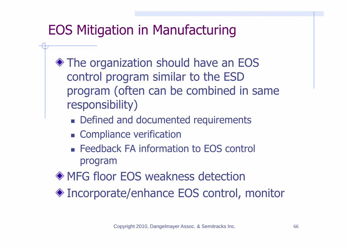
EOS Mitigation in Manufacturing
The organization should have an EOScontrol program similar to the ESDprogram (often can be combined in sameresponsibility)
Defined and documented requirements
Compliance verification
Feedback FA information to EOS controlprogram
MFG floor EOS weakness detection
Incorporate/enhance EOS control, monitor
66Copyright 2010, Dangelmayer Assoc. & Semitracks Inc.
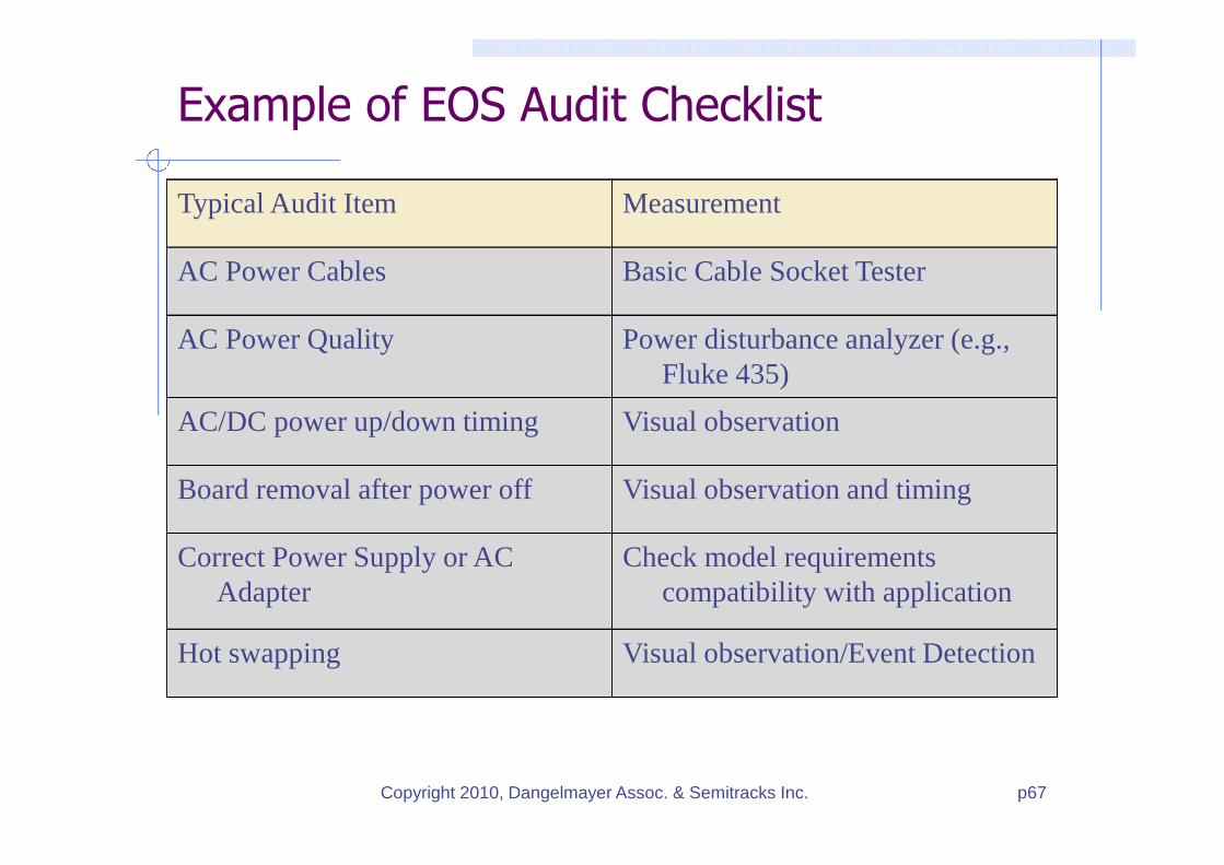
Example of EOS Audit Checklist
Typical Audit Item Measurement
AC Power Cables Basic Cable Socket Tester
AC Power Quality Power disturbance analyzer (e.g.,Fluke 435)
AC/DC power up/down timing Visual observation
Board removal after power off Visual observation and timing
Correct Power Supply or ACAdapter
Check model requirementscompatibility with application
Hot swapping Visual observation/Event Detection
p67Copyright 2010, Dangelmayer Assoc. & Semitracks Inc.
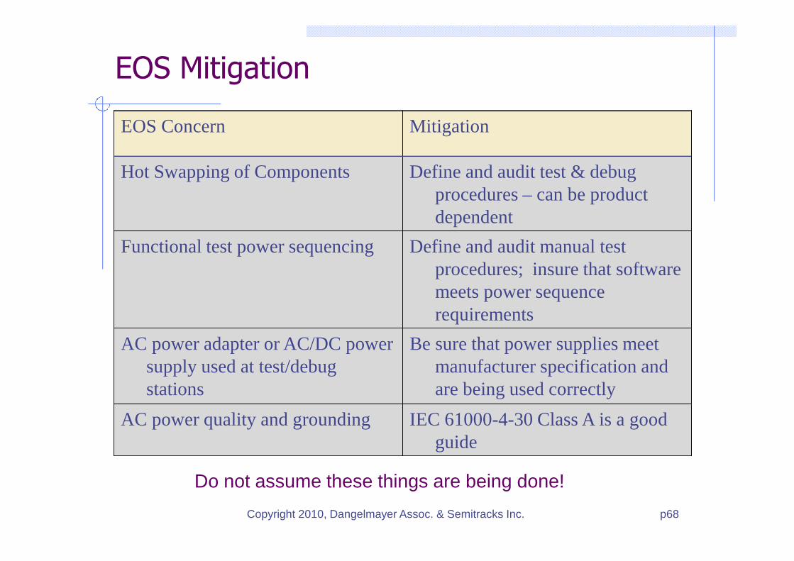
EOS Mitigation
EOS Concern Mitigation
Hot Swapping of Components Define and audit test & debugprocedures – can be productdependent
Functional test power sequencing Define and audit manual testprocedures; insure that softwaremeets power sequencerequirements
AC power adapter or AC/DC powersupply used at test/debugstations
Be sure that power supplies meetmanufacturer specification andare being used correctly
AC power quality and grounding IEC 61000-4-30 Class A is a goodguide
p68Copyright 2010, Dangelmayer Assoc. & Semitracks Inc.
Do not assume these things are being done!
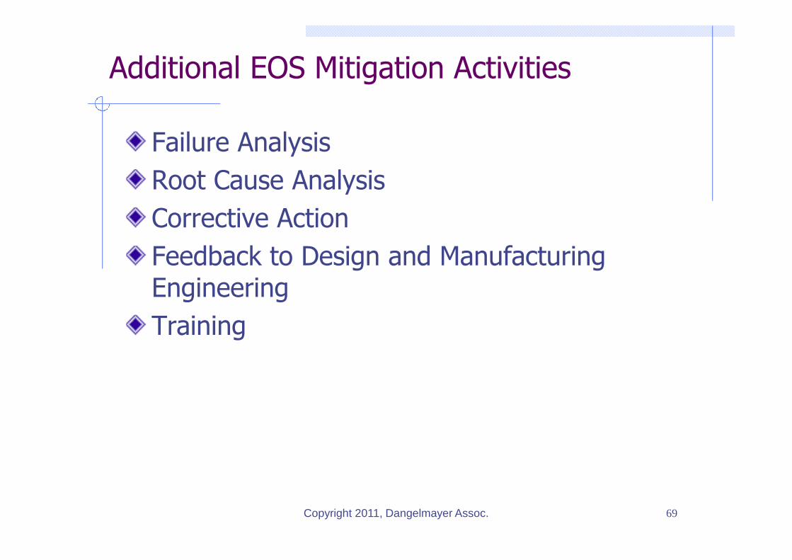
Additional EOS Mitigation Activities
Failure Analysis
Root Cause Analysis
Corrective Action
Feedback to Design and ManufacturingEngineering
Training
Copyright 2011, Dangelmayer Assoc. 69
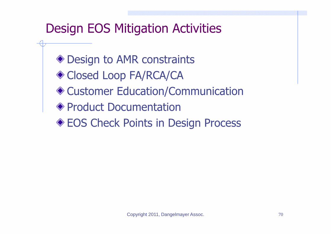
Design EOS Mitigation Activities
Design to AMR constraints
Closed Loop FA/RCA/CA
Customer Education/Communication
Product Documentation
EOS Check Points in Design Process
Copyright 2011, Dangelmayer Assoc. 70
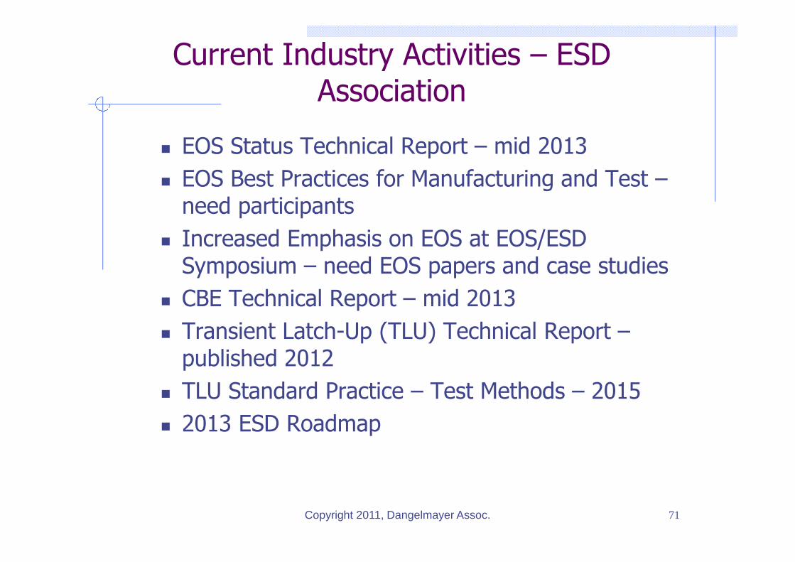
Current Industry Activities – ESDAssociation
EOS Status Technical Report – mid 2013
EOS Best Practices for Manufacturing and Test –need participants
Increased Emphasis on EOS at EOS/ESDSymposium – need EOS papers and case studies
CBE Technical Report – mid 2013
Transient Latch-Up (TLU) Technical Report –published 2012
TLU Standard Practice – Test Methods – 2015
2013 ESD Roadmap
Copyright 2011, Dangelmayer Assoc. 71
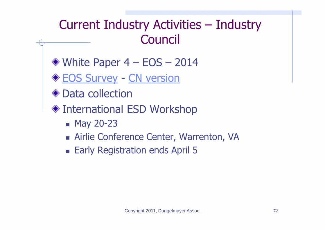
Current Industry Activities – IndustryCouncil
White Paper 4 – EOS – 2014
EOS Survey - CN version
Data collection
International ESD Workshop
May 20-23
Airlie Conference Center, Warrenton, VA
Early Registration ends April 5
Copyright 2011, Dangelmayer Assoc. 72
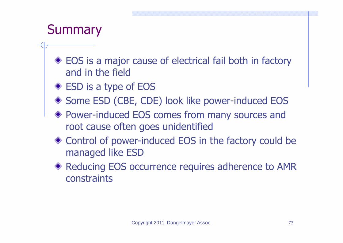
Summary
EOS is a major cause of electrical fail both in factoryand in the field
ESD is a type of EOS
Some ESD (CBE, CDE) look like power-induced EOS
Power-induced EOS comes from many sources androot cause often goes unidentified
Control of power-induced EOS in the factory could bemanaged like ESD
Reducing EOS occurrence requires adherence to AMRconstraints
Copyright 2011, Dangelmayer Assoc. 73
Significant Contributors
Chris Henderson
David Weir
Stephen Fairbanks
Andrew Olney
Alan Righter
Tim Maloney
Julian Montoya
Hans Kunz
p74Copyright 2010, Dangelmayer Assoc. & Semitracks Inc.
Jean-Luc Lefebvre
Lorenzo Cerati
Toni Gurga
Al Wallash
Vladimir Kraz
Reinhold Gaertner
Karim Kaschani


![Electrostatic Discharge/Electrical Overstress Susceptibility in .../67531/metadc721298/...MEMS devices such as optical mirrors [6]or printheads [7] are structurally-isolated structures](https://img.pdfslide.us/doc/110x75/612f12171ecc5158694335c8/electrostatic-dischargeelectrical-overstress-susceptibility-in-67531metadc721298.jpg)