Embed Size (px)
Citation preview
Rev. 1.00 Oct 2020
Renesas RA Family RA2 Series
User’
s Manual
www.renesas.com
All information contained in these materials, including products and product specifications, represents information on the product at the time of publication and is subject to change by Renesas Electronics Corp. without notice. Please review the latest information published by Renesas Electronics Corp. through various means, including the Renesas Electronics Corp. website (http://www.renesas.com).
RA2L1 Group
Evaluation Kit for RA2L1 Microcontroller Group EK-RA2L1 v1
User’s Manual
User’s M
anual
© 2020 Renesas Electronics Corporation. All rights reserved.
Notice 1. Descriptions of circuits, software and other related information in this document are provided only to illustrate the operation of semiconductor products
and application examples. You are fully responsible for the incorporation or any other use of the circuits, software, and information in the design of your product or system. Renesas Electronics disclaims any and all liability for any losses and damages incurred by you or third parties arising from the use of these circuits, software, or information.
2. Renesas Electronics hereby expressly disclaims any warranties against and liability for infringement or any other claims involving patents, copyrights, or other intellectual property rights of third parties, by or arising from the use of Renesas Electronics products or technical information described in this document, including but not limited to, the product data, drawings, charts, programs, algorithms, and application examples.
3. No license, express, implied or otherwise, is granted hereby under any patents, copyrights or other intellectual property rights of Renesas Electronics or others.
4. You shall not alter, modify, copy, or reverse engineer any Renesas Electronics product, whether in whole or in part. Renesas Electronics disclaims any and all liability for any losses or damages incurred by you or third parties arising from such alteration, modification, copying or reverse engineering.
5. Renesas Electronics products are classified according to the following two quality grades: “Standard” and “High Quality”. The intended applications for each Renesas Electronics product depends on the product’s quality grade, as indicated below. "Standard": Computers; office equipment; communications equipment; test and measurement equipment; audio and visual equipment; home
electronic appliances; machine tools; personal electronic equipment; industrial robots; etc. "High Quality": Transportation equipment (automobiles, trains, ships, etc.); traffic control (traffic lights); large-scale communication equipment; key
financial terminal systems; safety control equipment; etc. Unless expressly designated as a high reliability product or a product for harsh environments in a Renesas Electronics data sheet or other Renesas Electronics document, Renesas Electronics products are not intended or authorized for use in products or systems that may pose a direct threat to human life or bodily injury (artificial life support devices or systems; surgical implantations; etc.), or may cause serious property damage (space system; undersea repeaters; nuclear power control systems; aircraft control systems; key plant systems; military equipment; etc.). Renesas Electronics disclaims any and all liability for any damages or losses incurred by you or any third parties arising from the use of any Renesas Electronics product that is inconsistent with any Renesas Electronics data sheet, user’s manual or other Renesas Electronics document.
6. When using Renesas Electronics products, refer to the latest product information (data sheets, user’s manuals, application notes, “General Notes for Handling and Using Semiconductor Devices” in the reliability handbook, etc.), and ensure that usage conditions are within the ranges specified by Renesas Electronics with respect to maximum ratings, operating power supply voltage range, heat dissipation characteristics, installation, etc. Renesas Electronics disclaims any and all liability for any malfunctions, failure or accident arising out of the use of Renesas Electronics products outside of such specified ranges.
7. Although Renesas Electronics endeavors to improve the quality and reliability of Renesas Electronics products, semiconductor products have specific characteristics, such as the occurrence of failure at a certain rate and malfunctions under certain use conditions. Unless designated as a high reliability product or a product for harsh environments in a Renesas Electronics data sheet or other Renesas Electronics document, Renesas Electronics products are not subject to radiation resistance design. You are responsible for implementing safety measures to guard against the possibility of bodily injury, injury or damage caused by fire, and/or danger to the public in the event of a failure or malfunction of Renesas Electronics products, such as safety design for hardware and software, including but not limited to redundancy, fire control and malfunction prevention, appropriate treatment for aging degradation or any other appropriate measures. Because the evaluation of microcomputer software alone is very difficult and impractical, you are responsible for evaluating the safety of the final products or systems manufactured by you.
8. Please contact a Renesas Electronics sales office for details as to environmental matters such as the environmental compatibility of each Renesas Electronics product. You are responsible for carefully and sufficiently investigating applicable laws and regulations that regulate the inclusion or use of controlled substances, including without limitation, the EU RoHS Directive, and using Renesas Electronics products in compliance with all these applicable laws and regulations. Renesas Electronics disclaims any and all liability for damages or losses occurring as a result of your noncompliance with applicable laws and regulations.
9. Renesas Electronics products and technologies shall not be used for or incorporated into any products or systems whose manufacture, use, or sale is prohibited under any applicable domestic or foreign laws or regulations. You shall comply with any applicable export control laws and regulations promulgated and administered by the governments of any countries asserting jurisdiction over the parties or transactions.
10. It is the responsibility of the buyer or distributor of Renesas Electronics products, or any other party who distributes, disposes of, or otherwise sells or transfers the product to a third party, to notify such third party in advance of the contents and conditions set forth in this document.
11. This document shall not be reprinted, reproduced or duplicated in any form, in whole or in part, without prior written consent of Renesas Electronics. 12. Please contact a Renesas Electronics sales office if you have any questions regarding the information contained in this document or Renesas
Electronics products.
(Note1) “Renesas Electronics” as used in this document means Renesas Electronics Corporation and also includes its directly or indirectly controlled subsidiaries.
(Note2) “Renesas Electronics product(s)” means any product developed or manufactured by or for Renesas Electronics.
(Rev.4.0-1 November 2017)
Corporate Headquarters Contact information TOYOSU FORESIA, 3-2-24 Toyosu, Koto-ku, Tokyo 135-0061, Japan www.renesas.com
For further information on a product, technology, the most up-to-date version of a document, or your nearest sales office, please visit: www.renesas.com/contact/.
Trademarks Renesas and the Renesas logo are trademarks of Renesas Electronics Corporation. All trademarks and registered trademarks are the property of their respective owners.
General Precautions in the Handling of Microprocessing Unit and Microcontroller Unit Products The following usage notes are applicable to all Microprocessing unit and Microcontroller unit products from Renesas. For detailed usage notes on the products covered by this document, refer to the relevant sections of the document as well as any technical updates that have been issued for the products. 1. Precaution against Electrostatic Discharge (ESD)
A strong electrical field, when exposed to a CMOS device, can cause destruction of the gate oxide and ultimately degrade the device operation. Steps must be taken to stop the generation of static electricity as much as possible, and quickly dissipate it when it occurs. Environmental control must be adequate. When it is dry, a humidifier should be used. This is recommended to avoid using insulators that can easily build up static electricity. Semiconductor devices must be stored and transported in an anti-static container, static shielding bag or conductive material. All test and measurement tools including work benches and floors must be grounded. The operator must also be grounded using a wrist strap. Semiconductor devices must not be touched with bare hands. Similar precautions must be taken for printed circuit boards with mounted semiconductor devices.
2. Processing at power-on The state of the product is undefined at the time when power is supplied. The states of internal circuits in the LSI are indeterminate and the states of register settings and pins are undefined at the time when power is supplied. In a finished product where the reset signal is applied to the external reset pin, the states of pins are not guaranteed from the time when power is supplied until the reset process is completed. In a similar way, the states of pins in a product that is reset by an on-chip power-on reset function are not guaranteed from the time when power is supplied until the power reaches the level at which resetting is specified.
3. Input of signal during power-off state Do not input signals or an I/O pull-up power supply while the device is powered off. The current injection that results from input of such a signal or I/O pull-up power supply may cause malfunction and the abnormal current that passes in the device at this time may cause degradation of internal elements. Follow the guideline for input signal during power-off state as described in your product documentation.
4. Handling of unused pins Handle unused pins in accordance with the directions given under handling of unused pins in the manual. The input pins of CMOS products are generally in the high-impedance state. In operation with an unused pin in the open-circuit state, extra electromagnetic noise is induced in the vicinity of the LSI, an associated shoot-through current flows internally, and malfunctions occur due to the false recognition of the pin state as an input signal become possible.
5. Clock signals After applying a reset, only release the reset line after the operating clock signal becomes stable. When switching the clock signal during program execution, wait until the target clock signal is stabilized. When the clock signal is generated with an external resonator or from an external oscillator during a reset, ensure that the reset line is only released after full stabilization of the clock signal. Additionally, when switching to a clock signal produced with an external resonator or by an external oscillator while program execution is in progress, wait until the target clock signal is stable.
6. Voltage application waveform at input pin Waveform distortion due to input noise or a reflected wave may cause malfunction. If the input of the CMOS device stays in the area between VIL (Max.) and VIH (Min.) due to noise, for example, the device may malfunction. Take care to prevent chattering noise from entering the device when the input level is fixed, and also in the transition period when the input level passes through the area between VIL (Max.) and VIH (Min.).
7. Prohibition of access to reserved addresses Access to reserved addresses is prohibited. The reserved addresses are provided for possible future expansion of functions. Do not access these addresses as the correct operation of the LSI is not guaranteed.
8. Differences between products Before changing from one product to another, for example to a product with a different part number, confirm that the change will not lead to problems. The characteristics of a Microprocessing unit or microcontroller unit products in the same group but having a different part number might differ in terms of internal memory capacity, layout pattern, and other factors, which can affect the ranges of electrical characteristics, such as characteristic values, operating margins, immunity to noise, and amount of radiated noise. When changing to a product with a different part number, implement a system evaluation test for the given product.
Renesas EK-RA2L1 Disclaimer By using this EK-RA2L1, the User accepts the following terms, which are in addition to, and control in the event of disagreement, with Renesas’ General Terms and Conditions available at https://www.renesas.com/en-us/legal/disclaimer.html. The EK-RA2L1 is not guaranteed to be error free, and the entire risk as to the results and performance of the EK-RA2L1 is assumed by the User. The EK-RA2L1 is provided by Renesas on an “as is” basis without warranty of any kind whether express or implied, including but not limited to the implied warranties of good workmanship, fitness for a particular purpose, title, merchantability, and non-infringement of intellectual property rights. Renesas expressly disclaims any implied warranty. Renesas does not consider the EK-RA2L1 to be a finished product and therefore the EK-RA2L1 may not comply with some requirements applicable to finished products, including, but not limited to recycling, restricted substances and electromagnetic compatibility regulations. Refer to Certifications section, for information about certifications and compliance information for the EK-RA2L1. It is the kit User’s responsibility to make sure the kit meets any local requirements applicable to their region. Renesas or its affiliates shall in no event be liable for any loss of profit, loss of data, loss of contract, loss of business, damage to reputation or goodwill, any economic loss, any reprogramming or recall costs (whether the foregoing losses are direct or indirect) nor shall Renesas or its affiliates be liable for any other direct or indirect special, incidental or consequential damages arising out of or in relation to the use of this EK-RA2L1, even if Renesas or its affiliates have been advised of the possibility of such damages. Renesas has used reasonable care in preparing the information included in this document, but Renesas does not warrant that such information is error free nor does Renesas guarantee an exact match for every application or parameter to part numbers designated by other vendors listed herein. The information provided in this document is intended solely to enable the use of Renesas products. No express or implied license to any intellectual property right is granted by this document or in connection with the sale of Renesas products. Renesas reserves the right to make changes to specifications and product descriptions at any time without notice. Renesas assumes no liability for any damages incurred by you resulting from errors in or omissions from the information included herein. Renesas cannot verify, and assumes no liability for, the accuracy of information available on another company’s website.
Precautions This Evaluation Kit is only intended for use in a laboratory environment under ambient temperature and humidity conditions. A safe separation distance should be used between this and any sensitive equipment. Its use outside the laboratory, classroom, study area, or similar such area invalidates conformity with the protection requirements of the Electromagnetic Compatibility Directive and could lead to prosecution. The product generates, uses, and can radiate radio frequency energy and may cause harmful interference to radio communications. There is no guarantee that interference will not occur in a particular installation. If this equipment causes harmful interference to radio or television reception, which can be determined by turning the equipment off or on, you are encouraged to try to correct the interference by one or more of the following measures: • Ensure attached cables do not lie across the equipment. • Reorient the receiving antenna. • Increase the distance between the equipment and the receiver. • Connect the equipment into an outlet on a circuit different from that which the receiver is connected. • Power down the equipment when not in use. • Consult the dealer or an experienced radio/TV technician for help. Note: It is recommended that wherever possible shielded interface cables are used. The product is potentially susceptible to certain EMC phenomena. To mitigate against them it is recommended that the following measures be undertaken: • The user is advised that mobile phones should not be used within 10 m of the product when in use. • The user is advised to take ESD precautions when handling the equipment. The Evaluation Kit does not represent an ideal reference design for an end product and does not fulfil the regulatory standards for an end product.
User’s Manual
R20UT4827EG0100 Rev 1.00 Page 1 of 31 Oct.29.20
Renesas RA Family
EK-RA2L1 v1 Contents
1. Kit Overview ............................................................................................................................ 4 1.1 Assumptions and Advisory Notes ............................................................................................................ 6
2. Kit Contents ............................................................................................................................. 7
3. Kit Ordering Information ........................................................................................................... 7
4. Hardware Architecture and Default Configuration .................................................................... 8 4.1 Kit Architecture ........................................................................................................................................ 8 4.2 System Block Diagram .......................................................................................................................... 10 4.3 Jumper Settings ..................................................................................................................................... 11 4.3.1 Copper Jumpers .................................................................................................................................. 11 4.3.2 Traditional Pin Header Jumpers .......................................................................................................... 11 4.3.3 Default Jumper Configuration .............................................................................................................. 11
5. System Control and Ecosystem Access Area ........................................................................ 13 5.1 Power .................................................................................................................................................... 13 5.1.1 Power Supply Options ......................................................................................................................... 14 5.1.2 Power Supply Considerations ............................................................................................................. 14 5.1.3 Power-up Behavior .............................................................................................................................. 14 5.2 Debug and Trace ................................................................................................................................... 15 5.2.1 Debug On-Board ................................................................................................................................. 15 5.2.2 Debug In .............................................................................................................................................. 16 5.2.3 Debug Out ........................................................................................................................................... 18 5.3 Ecosystem ............................................................................................................................................. 18 5.3.1 Seeed Grove® Connectors .................................................................................................................. 18 5.3.2 SparkFun® Qwiic® Connector .............................................................................................................. 19 5.3.3 Digilent Pmod™ Connectors ............................................................................................................... 19 5.3.4 Arduino™ Connector ........................................................................................................................... 21 5.3.5 MikroElektronika™ mikroBUS Connector ........................................................................................... 23 5.4 Miscellaneous ........................................................................................................................................ 23 5.4.1 User and Power LEDs ......................................................................................................................... 23 5.4.2 User and Reset Switches .................................................................................................................... 24 5.4.3 MCU Boot Mode .................................................................................................................................. 25
6. MCU Native Pin Access Area ................................................................................................ 26 6.1 Breakout Pin Headers ........................................................................................................................... 26 6.2 MCU Current Measurement .................................................................................................................. 27
Renesas RA Family EK-RA2L1 v1 – User's Manual
R20UT4827EG0100 Rev 1.00 Page 2 of 31 Oct.29.20
6.3 MCU Internal Voltage Regulator ........................................................................................................... 27
7. Certifications .......................................................................................................................... 29 7.1 EMC/EMI Standards .............................................................................................................................. 29 7.2 Material Selection, Waste, Recycling and Disposal Standards ............................................................ 29 7.3 Safety Standards ................................................................................................................................... 29
8. Design and Manufacturing Information .................................................................................. 30
9. Website and Support ............................................................................................................. 30
Revision History ............................................................................................................................ 31
Figures Figure 1. EK-RA2L1 Board Top Side .............................................................................................................. 5 Figure 2. EK-RA2L1 Board Bottom Side ......................................................................................................... 6 Figure 3. EK-RA2L1 Kit Contents ..................................................................................................................... 7 Figure 4. EK-RA2L1 Board Functional Area Definitions .................................................................................. 9 Figure 5. EK-RA2L1 Board Block Diagram ................................................................................................... 10 Figure 6. Copper Jumpers ............................................................................................................................. 11 Figure 7. System Control and Ecosystem Access Area ................................................................................ 13 Figure 8. Power Supply Options .................................................................................................................... 14 Figure 9. EK-RA2L1 Debug Interface ............................................................................................................ 16 Figure 10. Seeed Grove and Qwiic Connectors ............................................................................................ 19 Figure 11. Pmod 1 ......................................................................................................................................... 20 Figure 12. Pmod 1 Trace Cut Jumpers ......................................................................................................... 20 Figure 13. Pmod 2 ......................................................................................................................................... 21 Figure 14. Arduino Uno Connectors .............................................................................................................. 22 Figure 15. mikroBUS Connection .................................................................................................................. 23 Figure 16. User LEDs .................................................................................................................................... 24 Figure 17. Power LED ................................................................................................................................... 24 Figure 18. Reset and User Switches ............................................................................................................. 25 Figure 19. Boot Mode .................................................................................................................................... 25 Figure 20. Native Pin Access Area ................................................................................................................ 26 Figure 21. RA +3.3 V Current Measurement Circuit...................................................................................... 27 Figure 22. RA MCU Current Measurement ................................................................................................... 27 Figure 23. RA MCU Internal Regulator Circuit .............................................................................................. 27
Tables Table 1. Default Jumper Settings ................................................................................................................ 11 Table 2. Debug Modes ................................................................................................................................ 15
Renesas RA Family EK-RA2L1 v1 – User's Manual
R20UT4827EG0100 Rev 1.00 Page 3 of 31 Oct.29.20
Table 3. Jumper Connection Summary for Different Debug Modes ........................................................... 15 Table 4. Debug USB Connector .................................................................................................................. 15 Table 5. Debug On-Board Jumper Configuration ........................................................................................ 16 Table 6. Debug In Mode Jumper Configuration .......................................................................................... 16 Table 7. JTAG/SWD/TRACE Connector ..................................................................................................... 17 Table 8. JTAG/SWD Connector .................................................................................................................. 17 Table 9. Debug Out Jumper Configuration .................................................................................................. 18 Table 10. Grove 1 Connector ..................................................................................................................... 18 Table 11. Grove 2 Connector ..................................................................................................................... 18 Table 12. Qwiic Connector ......................................................................................................................... 19 Table 13. Pmod 1 Connector ..................................................................................................................... 19 Table 14. Pmod 2 Connector ..................................................................................................................... 21 Table 15. Arduino Uno Connections .......................................................................................................... 21 Table 16. mikroBUS Connections .............................................................................................................. 23 Table 17. EK-RA2L1 Board LED Functions ............................................................................................... 23 Table 18. EK-RA2L1 Board Switches ........................................................................................................ 24 Table 19. EK-RA2L1 Internal Regulator Settings ...................................................................................... 28 Table 20. EK-RA2L1 Board Design Package Contents ............................................................................. 30
Renesas RA Family EK-RA2L1 v1 – User's Manual
R20UT4827EG0100 Rev 1.00 Page 4 of 31 Oct.29.20
1. Kit Overview The EK-RA2L1, an Evaluation Kit for RA2L1 MCU Group, enables users to seamlessly evaluate the features of the RA2L1 MCU group and develop embedded systems applications using Flexible Software Package (FSP) and e2 studio IDE. The users can utilize rich on-board features along with their choice of popular ecosystems add-ons to bring their big ideas to life.
The key features of the EK-RA2L1 board are categorized in the following groups (consistent with the architecture of the kit) as follows:
MCU Native Pin Access • R7FA2L1AB2DFP MCU (referred to as RA MCU) • 48 MHz, Arm® Cortex®-M23 core • 256 kB Code Flash, 32 kB SRAM • 100 pins, LQFP package • Native pin access through 1 x 40-pin and 3 x 20-pin male headers • MCU current measurement points for precision current consumption measurement • Multiple clock sources – Low-precision clocks are available internal to the RA MCU. Additionally, RA
MCU oscillator and sub-clock oscillator crystals, 20.000 MHz and 32,768 Hz, are provided for precision • Internal MCU DC-DC power option System Control and Ecosystem Access • Two 5 V input sources
USB (Debug) External power supply (using surface mount clamp test points and power input vias)
• Three Debug modes Debug on-board (SWD) Debug in (ETM, SWD, and JTAG) Debug out (SWD)
• User LEDs and buttons Three User LEDs (red, blue, green) Power LED (white) indicating availability of regulated power Debug LED (yellow) indicating the debug connection Two User buttons One Reset button
• Five most popular ecosystems expansions 2 Seeed Grove® system (I2C/Analog) connectors SparkFun® Qwiic® connector 2 Digilent PmodTM (SPI and UART) connectors ArduinoTM (Uno R3) connector MikroElektronikaTM mikroBUS connector
• MCU boot configuration jumper
Renesas RA Family EK-RA2L1 v1 – User's Manual
R20UT4827EG0100 Rev 1.00 Page 5 of 31 Oct.29.20
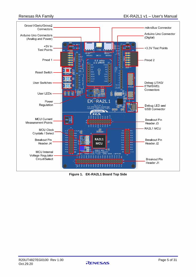
Figure 1. EK-RA2L1 Board Top Side
Renesas RA Family EK-RA2L1 v1 – User's Manual
R20UT4827EG0100 Rev 1.00 Page 6 of 31 Oct.29.20
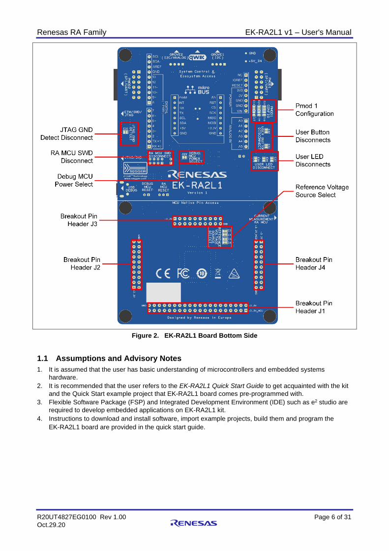
Figure 2. EK-RA2L1 Board Bottom Side
1.1 Assumptions and Advisory Notes 1. It is assumed that the user has basic understanding of microcontrollers and embedded systems
hardware. 2. It is recommended that the user refers to the EK-RA2L1 Quick Start Guide to get acquainted with the kit
and the Quick Start example project that EK-RA2L1 board comes pre-programmed with. 3. Flexible Software Package (FSP) and Integrated Development Environment (IDE) such as e2 studio are
required to develop embedded applications on EK-RA2L1 kit. 4. Instructions to download and install software, import example projects, build them and program the
EK-RA2L1 board are provided in the quick start guide.
Renesas RA Family EK-RA2L1 v1 – User's Manual
R20UT4827EG0100 Rev 1.00 Page 7 of 31 Oct.29.20
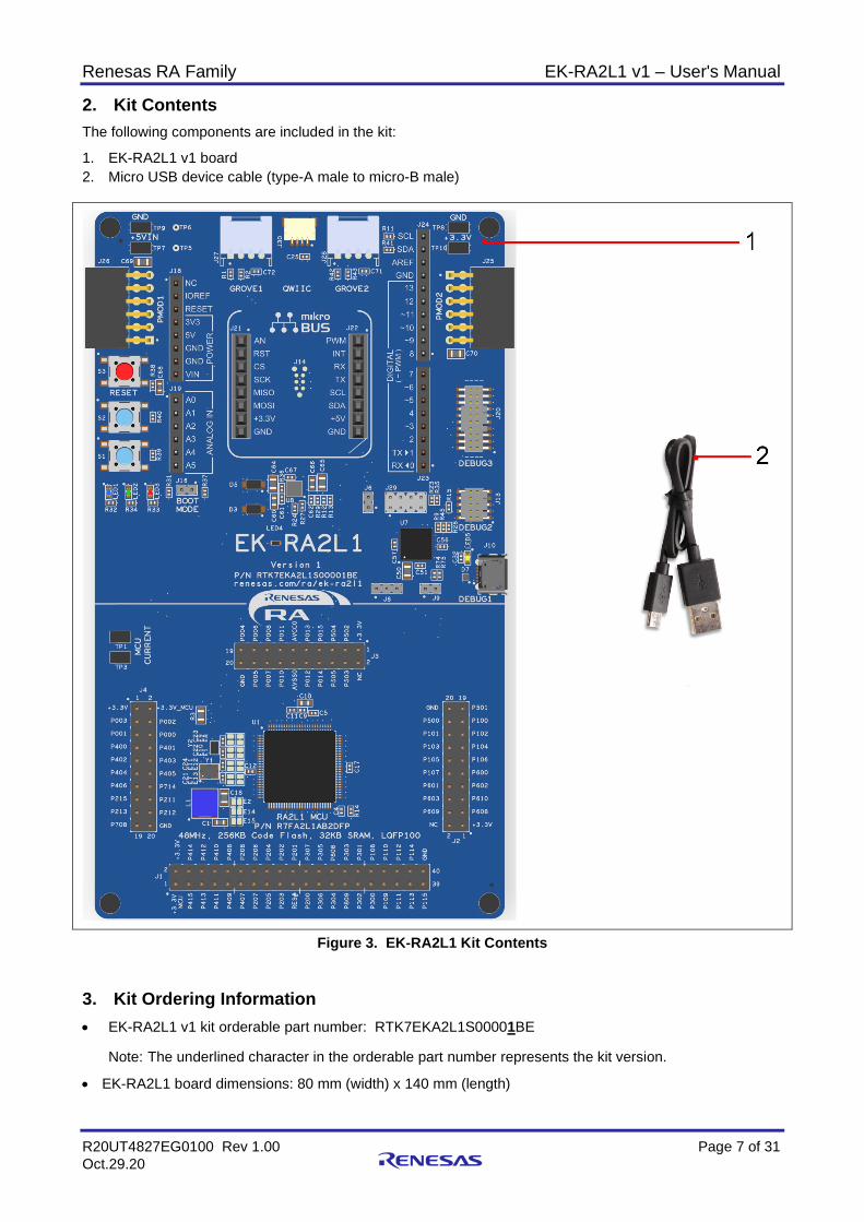
2. Kit Contents The following components are included in the kit:
1. EK-RA2L1 v1 board 2. Micro USB device cable (type-A male to micro-B male)
Figure 3. EK-RA2L1 Kit Contents
3. Kit Ordering Information • EK-RA2L1 v1 kit orderable part number: RTK7EKA2L1S00001BE
Note: The underlined character in the orderable part number represents the kit version.
• EK-RA2L1 board dimensions: 80 mm (width) x 140 mm (length)
Renesas RA Family EK-RA2L1 v1 – User's Manual
R20UT4827EG0100 Rev 1.00 Page 8 of 31 Oct.29.20
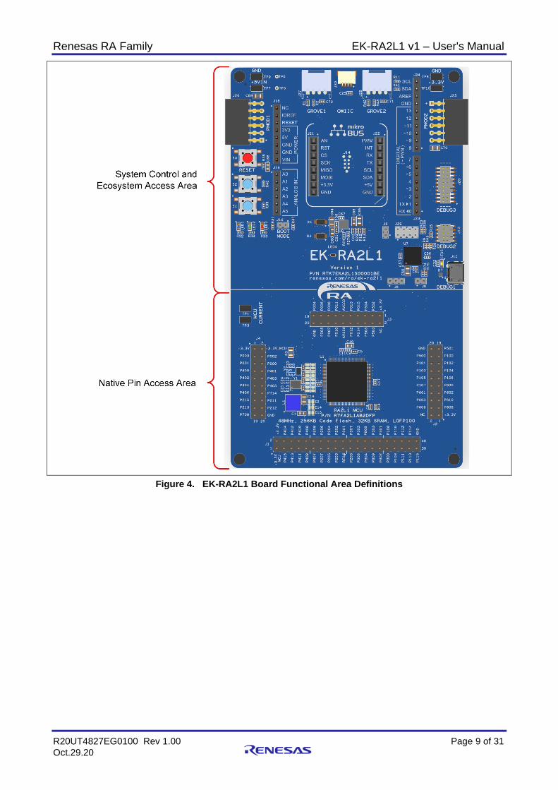
4. Hardware Architecture and Default Configuration 4.1 Kit Architecture The EK-RA2L1 board is designed with two of three sections or areas to help shorten the learning curve of the users and maximize the design and knowledge reuse among similar kits. The contents of these three areas are conceptually standardized among similar kits.
Kit area Area features Area present on all similar kits
Functionality is:
MCU Native Pin Access Area
RA MCU, breakout pin headers for all MCU I/O and power, current measurement
Yes MCU dependent
Special Feature Access Area (not present on EK-RA2L1)
MCU special features: None Optional MCU dependent
System Control and Ecosystem Access Area
Power, Debug MCU, User LED and buttons, reset, ecosystem connectors, USB Full Speed Host and Device, Boot configuration
Yes Same or similar across similar kits
Renesas RA Family EK-RA2L1 v1 – User's Manual
R20UT4827EG0100 Rev 1.00 Page 9 of 31 Oct.29.20
Figure 4. EK-RA2L1 Board Functional Area Definitions
Renesas RA Family EK-RA2L1 v1 – User's Manual
R20UT4827EG0100 Rev 1.00 Page 10 of 31 Oct.29.20
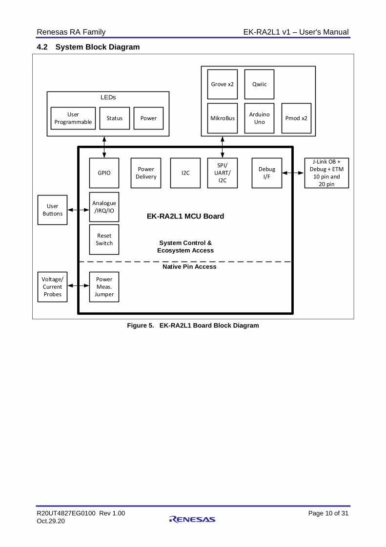
4.2 System Block Diagram
Figure 5. EK-RA2L1 Board Block Diagram
LEDs
Voltage/Current Probes
User Buttons
J-Link OB + Debug + ETM
10 pin and20 pin
User Programmable Status Power Pmod x2
Grove x2 Qwiic
MikroBus Arduino Uno
DebugI/FGPIO Power
Delivery
SPI/ UART/
I2C
Analogue/IRQ/IO
Reset Switch
Power Meas.
Jumper
EK-RA2L1 MCU Board
System Control & Ecosystem Access
Native Pin Access
I2C
Renesas RA Family EK-RA2L1 v1 – User's Manual
R20UT4827EG0100 Rev 1.00 Page 11 of 31 Oct.29.20
4.3 Jumper Settings Two types of jumpers are provided on the EK-RA2L1 board.
1. Copper jumpers (trace-cut type and solder bridge type) 2. Traditional pin header jumpers The following sections describe each type and their default configuration.
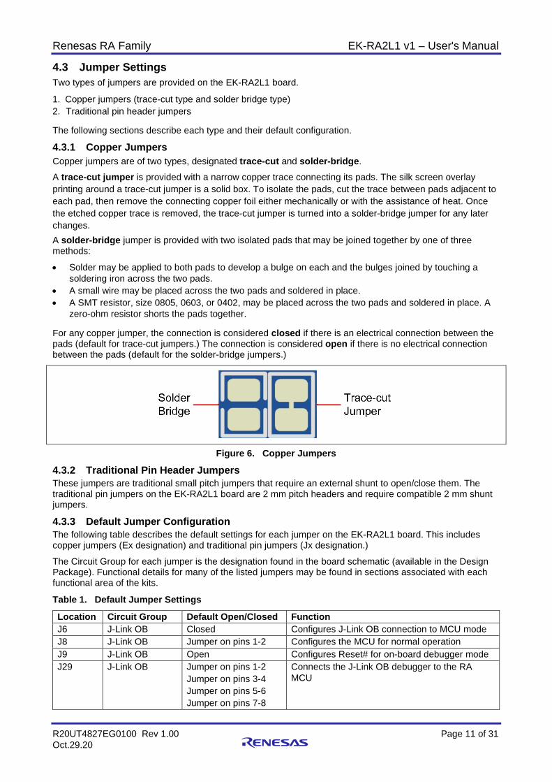
4.3.1 Copper Jumpers Copper jumpers are of two types, designated trace-cut and solder-bridge.
A trace-cut jumper is provided with a narrow copper trace connecting its pads. The silk screen overlay printing around a trace-cut jumper is a solid box. To isolate the pads, cut the trace between pads adjacent to each pad, then remove the connecting copper foil either mechanically or with the assistance of heat. Once the etched copper trace is removed, the trace-cut jumper is turned into a solder-bridge jumper for any later changes. A solder-bridge jumper is provided with two isolated pads that may be joined together by one of three methods:
• Solder may be applied to both pads to develop a bulge on each and the bulges joined by touching a soldering iron across the two pads.
• A small wire may be placed across the two pads and soldered in place. • A SMT resistor, size 0805, 0603, or 0402, may be placed across the two pads and soldered in place. A
zero-ohm resistor shorts the pads together. For any copper jumper, the connection is considered closed if there is an electrical connection between the pads (default for trace-cut jumpers.) The connection is considered open if there is no electrical connection between the pads (default for the solder-bridge jumpers.)
Figure 6. Copper Jumpers
4.3.2 Traditional Pin Header Jumpers These jumpers are traditional small pitch jumpers that require an external shunt to open/close them. The traditional pin jumpers on the EK-RA2L1 board are 2 mm pitch headers and require compatible 2 mm shunt jumpers.
4.3.3 Default Jumper Configuration The following table describes the default settings for each jumper on the EK-RA2L1 board. This includes copper jumpers (Ex designation) and traditional pin jumpers (Jx designation.)
The Circuit Group for each jumper is the designation found in the board schematic (available in the Design Package). Functional details for many of the listed jumpers may be found in sections associated with each functional area of the kits.
Table 1. Default Jumper Settings
Location Circuit Group Default Open/Closed Function J6 J-Link OB Closed Configures J-Link OB connection to MCU mode J8 J-Link OB Jumper on pins 1-2 Configures the MCU for normal operation J9 J-Link OB Open Configures Reset# for on-board debugger mode J29 J-Link OB Jumper on pins 1-2
Jumper on pins 3-4 Jumper on pins 5-6 Jumper on pins 7-8
Connects the J-Link OB debugger to the RA MCU
Renesas RA Family EK-RA2L1 v1 – User's Manual
R20UT4827EG0100 Rev 1.00 Page 12 of 31 Oct.29.20
Location Circuit Group Default Open/Closed Function J16 MCU Boot Mode Open Configures the MCU for normal boot mode E3 MCU Power Closed Connects AVCC0 to +3.3 V E4 MCU Power Closed Connects AVSS0 to GND E5 MCU Power Closed Connects P011/VREFL0 to GND E6 MCU Power Closed Connects P010/VREFH0 to +3.3 V E7 MCU Clock Open Connects P212/EXTAL to 20 MHz crystal E11 MCU Clock Open Connects P213/XTAL to 20 MHz crystal E13 MCU Clock Closed Connects P212/EXTAL pin to pin headers E12 MCU Clock Closed Connects P213/XTAL pin to pin headers E9 MCU Clock Open Connects P215/XCIN to 32 kHz crystal E10 MCU Clock Open Connects P214/XCOUT to 32 kHz crystal E1 MCU Clock Closed Connects P214/XCOUT to pin headers E8 MCU Clock Closed Connects P215/XCIN to pin headers E27 User LED Closed Connects P503 to User LED1 E26 User LED Closed Connects P504 to User LED2 E28 User LED Closed Connects P505 to User LED3 E29 Debug MCU
Power Closed Connects the Debug MCU power to +3.3 V
E30 JTAG Closed Connects the JTAG GND Detect pin on J20 and J13 to GND
E31 User Switch Closed Connects P004 to User Switch S1 E32 User Switch Closed Connects P015 to User Switch S2 E2 MCU Internal
Regulator Power Open Connects VSS_DCDC to GND
E14 MCU Internal Regulator Power
Open Connects VLO to power inductor
E15 MCU Internal Regulator Power
Open Connects VCC_DCDC to +3.3 V
E20 Pmod 1 Closed Connects P100 (MISOA/RXD0) to Pmod 1 E21 Pmod 1 Closed Connects P102 (RSPCKA/SCK0) to Pmod 1 E16 Pmod 1 Closed Connects +3.3 V to Pmod 1 E18 Pmod 1 Open Connects P301 (SCL2) to Pmod 1 E19 Pmod 1 Open Connects P302 (SDA2) to Pmod 1 E17 Pmod 1 Open Connects +5.0V to Pmod 1
Renesas RA Family EK-RA2L1 v1 – User's Manual
R20UT4827EG0100 Rev 1.00 Page 13 of 31 Oct.29.20
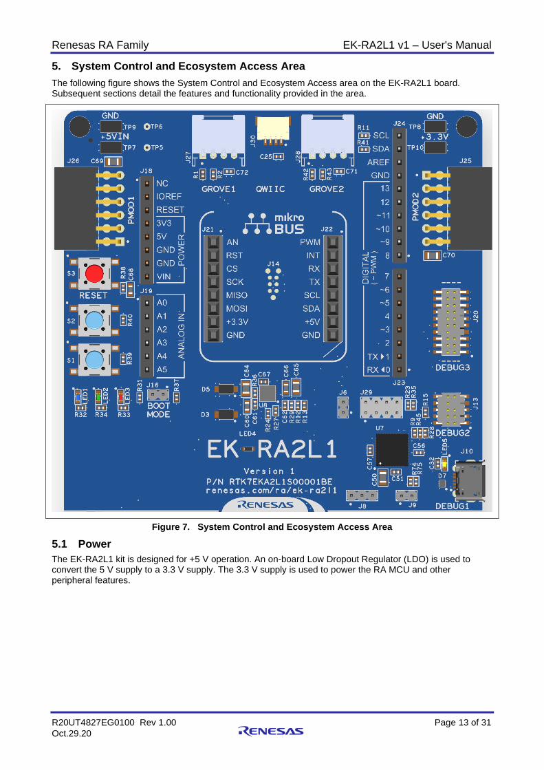
5. System Control and Ecosystem Access Area The following figure shows the System Control and Ecosystem Access area on the EK-RA2L1 board. Subsequent sections detail the features and functionality provided in the area.
Figure 7. System Control and Ecosystem Access Area
5.1 Power The EK-RA2L1 kit is designed for +5 V operation. An on-board Low Dropout Regulator (LDO) is used to convert the 5 V supply to a 3.3 V supply. The 3.3 V supply is used to power the RA MCU and other peripheral features.

Renesas RA Family EK-RA2L1 v1 – User's Manual
R20UT4827EG0100 Rev 1.00 Page 14 of 31 Oct.29.20
5.1.1 Power Supply Options This section describes the different ways in which EK-RA2L1 kit can be powered.
Figure 8. Power Supply Options
5.1.1.1 Option 1: Debug USB 5 V may be supplied from an external USB host to the USB Debug connector (J10) labelled DEBUG on the board. Power from this source is connected to the Main System 5 V Power. Reverse current protection is provided between this connector and the Main System 5 V Power.
5.1.1.2 Option 2: 5 V Test Points 5 V may be supplied from an external power supply to test points on the board. TP7 (5 V) and TP9 (GND) are loop-style test points, and TP5 (5 V) and TP6 (GND) are large via style test points. The two types of test points are electrically equivalent, and both are provided for user convenience. Power from this source is connected to the Main System 5 V Power. Reverse current protection is provided between the 5 V test points and the Main System 5 V Power.
5.1.2 Power Supply Considerations The on-board LDO regulator which supplies +3.3 V has a built-in current limit of 2.0 A. Make sure the total current required by the RA MCU, any active on-board features, and any connected peripheral devices does not exceed this limit.
Note: The total current available from a typical USB host is 500 mA maximum. Depending on the configuration of the kit, multiple power sources may be required.
5.1.3 Power-up Behavior When powered, the white LED near the center of the board (the “dash” in the EK-RA2L1 name) will light up. For more details on initial power up behavior, see the EK-RA2L1 Quick Start Guide.
5 V to 3.3 V Voltage
Regulator
Option 1: Debug USB
(J10)
3.3 V Voltage Measurement:TP8 and TP10
MCU Current Measurement
(R3) TP1 and TP3
Main System 3.3 V Power
RA MCU
Main Power
Main System5 V Power
Option 2a: TP5 and TP6
Option 2b: TP7 and TP9
Renesas RA Family EK-RA2L1 v1 – User's Manual
R20UT4827EG0100 Rev 1.00 Page 15 of 31 Oct.29.20
5.2 Debug and Trace The EK-RA2L1 board supports the following three debug modes.
Table 2. Debug Modes
Debug Modes
Debug MCU (one that connects to the IDE on PC)
Target MCU (one that is being debugged)
Debugging Interface/Protocol
Connector Used
Debug on-board
S124 (on-board) RA2L1 (on-board) SWD Micro USB (J10)
Debug in External debugging tools
RA2L1 (on-board) SWD, ETM, JTAG 20-pin connector (J20) or 10-pin connector (J13)
Debug out S124 (on-board) Any external RA MCU
SWD Micro USB (J10) plus either 20-pin connector (J20) or 10-pin connector (J13)
Notes: • See Table 4 for the Debug USB connector pin definition. • See Table 7 for the 20-pin JTAG connector pin definition. • See Table 8 for the 10-pin JTAG connector pin definition. The following table summarizes the jumper setting for each of the debug modes.
Table 3. Jumper Connection Summary for Different Debug Modes
Debug Modes J6 J8 J9 J29 Debug on-board Closed Jumper on pins 1-2 Open Jumpers on pins 1-2, 3-4, 5-6, 7-8 Debug in Closed Jumper on pins 1-2 Closed Jumpers on pins 1-2, 3-4, 5-6, 7-8 Debug out Open Jumper on pins 2-3 Open All pins open
5.2.1 Debug On-Board The on-board debug functionality is provided using Renesas S124 Debug MCU and SEGGER J-Link® firmware. Debug USB Micro-B connector (J10) connects the S124 Debug MCU to an external USB Full Speed Host, allowing re-programming and debugging of the target RA MCU firmware. This connection is the default debug mode for the EK-RA2L1 board.
The S124 Debug MCU connects to the target RA MCU using the SWD interface.
Table 4. Debug USB Connector
Debug USB Connector EK-RA2L1 Pin Description Signal/Bus J10-1 +5VDC +5V_USB_DBG J10-2 Data- USB_DM (U7-12) J10-3 Data+ USB_DP (U7-13) J10-4 USB ID, jack internal switch, cable inserted N.C. J10-5 Ground GND
A yellow indicator, LED5, shows the visual status of the debug interface. When the EK-RA2L1 board is powered on, and LED5 is blinking, it indicates that the S124 Debug MCU is not connected to a programming host. When LED5 is on solid, it indicates that the S124 Debug MCU is connected to a programming interface.
Renesas RA Family EK-RA2L1 v1 – User's Manual
R20UT4827EG0100 Rev 1.00 Page 16 of 31 Oct.29.20
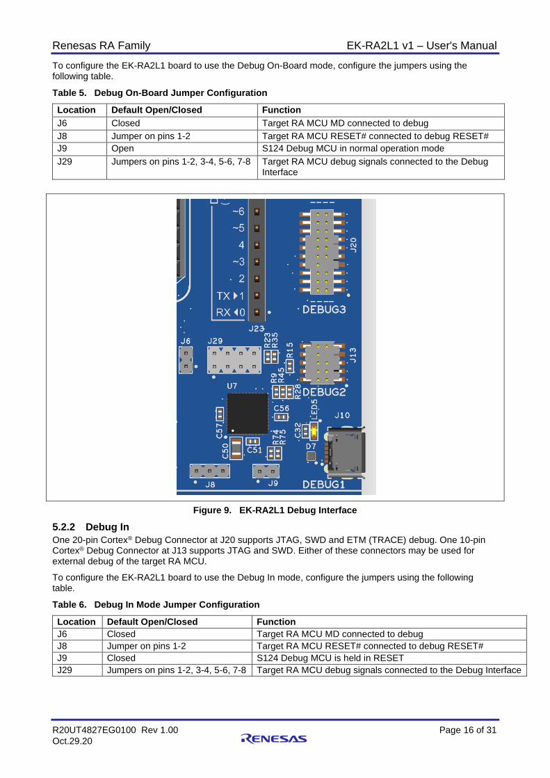
To configure the EK-RA2L1 board to use the Debug On-Board mode, configure the jumpers using the following table.
Table 5. Debug On-Board Jumper Configuration
Location Default Open/Closed Function J6 Closed Target RA MCU MD connected to debug J8 Jumper on pins 1-2 Target RA MCU RESET# connected to debug RESET# J9 Open S124 Debug MCU in normal operation mode J29 Jumpers on pins 1-2, 3-4, 5-6, 7-8 Target RA MCU debug signals connected to the Debug
Interface
Figure 9. EK-RA2L1 Debug Interface
5.2.2 Debug In One 20-pin Cortex® Debug Connector at J20 supports JTAG, SWD and ETM (TRACE) debug. One 10-pin Cortex® Debug Connector at J13 supports JTAG and SWD. Either of these connectors may be used for external debug of the target RA MCU.
To configure the EK-RA2L1 board to use the Debug In mode, configure the jumpers using the following table.
Table 6. Debug In Mode Jumper Configuration
Location Default Open/Closed Function J6 Closed Target RA MCU MD connected to debug J8 Jumper on pins 1-2 Target RA MCU RESET# connected to debug RESET# J9 Closed S124 Debug MCU is held in RESET J29 Jumpers on pins 1-2, 3-4, 5-6, 7-8 Target RA MCU debug signals connected to the Debug Interface

Renesas RA Family EK-RA2L1 v1 – User's Manual
R20UT4827EG0100 Rev 1.00 Page 17 of 31 Oct.29.20
Table 7. JTAG/SWD/TRACE Connector
JTAG Connector EK-RA2L1 Pin JTAG Pin Name SWD Pin Name ETM Pin Name Signal/Bus J20-1 Vtref Vtref Vtref +3V3 J20-2 TMS SWDIO N/A P108/SWDIO J20-3 GND GND GND GND J20-4 TCK SWCLK N/A P300/SWCLK J20-5 GND GND GND GND J20-6 TDO SWO N/A N/A J20-7 Key Key Key N.C. J20-8 TDI NC/EXTb N/A N/A J20-9 GNDDetect GNDDetect GNDDetect GND (cut E30 to open) J20-10 nSRST nSRST nSRST RESET# J20-11 N/A N/A N/A GND J20-12 N/A N/A TCLK N.C. J20-13 N/A N/A N/A GND J20-14 N/A N/A TDATA0 N.C. J20-15 N/A N/A GND GND J20-16 N/A N/A TDATA1 N.C. J20-17 N/A N/A GND GND J20-18 N/A N/A TDATA2 N.C. J20-19 N/A N/A GND GND J20-20 N/A N/A TDATA3 N.C.
Table 8. JTAG/SWD Connector
JTAG Connector EK-RA2L1 Pin JTAG Pin Name SWD Pin Name ETM Pin Name Signal/Bus J13-1 Vtref Vtref Vtref +3V3 J13-2 TMS SWDIO N/A P108/SWDIO J13-3 GND GND GND GND J13-4 TCK SWCLK N/A P300/SWCLK J13-5 GND GND GND GND J13-6 TDO SWO N/A N/A J13-7 Key Key Key N.C. J13-8 TDI NC/EXTb N/A N/A J13-9 GNDDetect GNDDetect GNDDetect GND (cut E30 to open) J13-10 nSRST nSRST nSRST RESET# (via J8)
Note: The Cortex® Debug Connector is fully described in the Arm® CoreSight™ Architecture Specification.
Renesas RA Family EK-RA2L1 v1 – User's Manual
R20UT4827EG0100 Rev 1.00 Page 18 of 31 Oct.29.20
5.2.3 Debug Out The EK-RA2L1 board can be configured to use the S124 Debug MCU to debug target RA MCU on an external board.
A yellow indicator, LED5, shows the visual status of the debug interface. When the EK-RA2L1 board is powered on, and LED5 is blinking, this indicates that the S124 Debug MCU is not connected to a programming host. When LED5 is on solid, this indicates that the S124 Debug MCU is connected to a programming interface.
To configure the EK-RA2L1 board to use the Debug Out mode, configure the jumpers according to the following table.
Table 9. Debug Out Jumper Configuration
Location Default Open/Closed Function J6 Open No connection to RA MCU J8 Jumper on pins 2-3 On-board RA MCU is held in RESET J9 Open S124 Debug MCU in normal operation mode J29 All jumpers removed Disconnects the on-board RA MCU debug signals from the
Debug Interface
5.3 Ecosystem The System Control and Ecosystem area provides users the option to simultaneously connect several 3rd party add-on modules compatible with four most popular ecosystems using the following connectors:
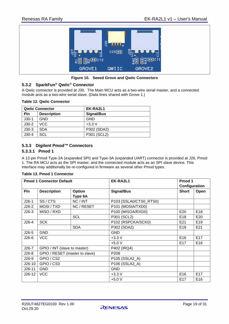
1. Two Seeed Grove® system (I2C/Analog) connectors 2. SparkFun® Qwiic® connector 3. Two Digilent Pmod™ (SPI and UART) connectors 4. Arduino™ (Uno R3) connector 5. MikroElektronika™ mikroBUS connector 5.3.1 Seeed Grove® Connectors 5.3.1.1 Grove 1 A Seeed Grove I2C connector is provided at J27. The RA MCU acts as a two-wire serial master, and a connected module acts as a two-wire serial slave.
Table 10. Grove 1 Connector
Grove 1 Connector EK-RA2L1 Pin Description Signal/Bus J27-1 SCL P301 (SCL2) J27-2 SDA P302 (SDA2) J27-3 VCC +3.3 V J27-4 GND GND
5.3.1.2 Grove 2 A Seeed Grove I2C/Analog connector is provided at J28. The RA MCU acts as a two-wire serial master, and a connected module acts as a two-wire serial slave.
The pull-up resistors, R42 and R43, must be fitted when using I2C and removed when using as analog.
Table 11. Grove 2 Connector
Grove 2 Connector EK-RA2L1 Pin Description Signal/Bus J28-1 SCL P502 (SCL1/AN018) J28-2 SDA P501 (SDA1/AN017) J28-3 VCC +3.3 V J28-4 GND GND
Renesas RA Family EK-RA2L1 v1 – User's Manual
R20UT4827EG0100 Rev 1.00 Page 19 of 31 Oct.29.20
Figure 10. Seeed Grove and Qwiic Connectors
5.3.2 SparkFun® Qwiic® Connector A Qwiic connector is provided at J30. The Main MCU acts as a two-wire serial master, and a connected module acts as a two-wire serial slave. (Data lines shared with Grove 1.)
Table 12. Qwiic Connector
Qwiic Connector EK-RA2L1 Pin Description Signal/Bus J30-1 GND GND J30-2 VCC +3.3 V J30-3 SDA P302 (SDA2) J30-4 SCL P301 (SCL2)
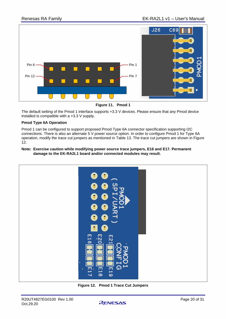
5.3.3 Digilent Pmod™ Connectors 5.3.3.1 Pmod 1 A 12-pin Pmod Type-2A (expanded SPI) and Type-3A (expanded UART) connector is provided at J26, Pmod 1. The RA MCU acts as the SPI master, and the connected module acts as an SPI slave device. This interface may additionally be re-configured in firmware as several other Pmod types.
Table 13. Pmod 1 Connector
Pmod 1 Connector Default EK-RA2L1 Pmod 1 Configuration
Pin Description Option Type 6A
Signal/Bus Short Open
J26-1 SS / CTS NC / INT P103 (SSLA0/CTS0_RTS0) J26-2 MOSI / TXD NC / RESET P101 (MOSIA/TXD0) J26-3
MISO / RXD P100 (MISOA/RXD0) E20 E18 SCL P301 (SCL2) E18 E20
J26-4
SCK P102 (RSPCKA/SCK0) E21 E19 SDA P302 (SDA2) E19 E21
J26-5 GND GND J26-6
VCC
+3.3 V E16 E17 +5.0 V E17 E16
J26-7 GPIO / INT (slave to master) P402 (IRQ4) J26-8 GPIO / RESET (master to slave) P208 J26-9 GPIO / CS2 P105 (SSLA2_A) J26-10 GPIO / CS3 P106 (SSLA3_A) J26-11 GND GND J26-12
VCC
+3.3 V E16 E17 +5.0 V E17 E16
Renesas RA Family EK-RA2L1 v1 – User's Manual
R20UT4827EG0100 Rev 1.00 Page 20 of 31 Oct.29.20
Figure 11. Pmod 1 The default setting of the Pmod 1 interface supports +3.3 V devices. Please ensure that any Pmod device installed is compatible with a +3.3 V supply.
Pmod Type 6A Operation Pmod 1 can be configured to support proposed Pmod Type 6A connector specification supporting I2C connections. There is also an alternate 5 V power source option. In order to configure Pmod 1 for Type 6A operation, modify the trace cut jumpers as mentioned in Table 13. The trace cut jumpers are shown in Figure 12.
Note: Exercise caution while modifying power source trace jumpers, E16 and E17. Permanent damage to the EK-RA2L1 board and/or connected modules may result.
Figure 12. Pmod 1 Trace Cut Jumpers
Pin 1
Pin 7
Pin 6
Pin 12
Renesas RA Family EK-RA2L1 v1 – User's Manual
R20UT4827EG0100 Rev 1.00 Page 21 of 31 Oct.29.20
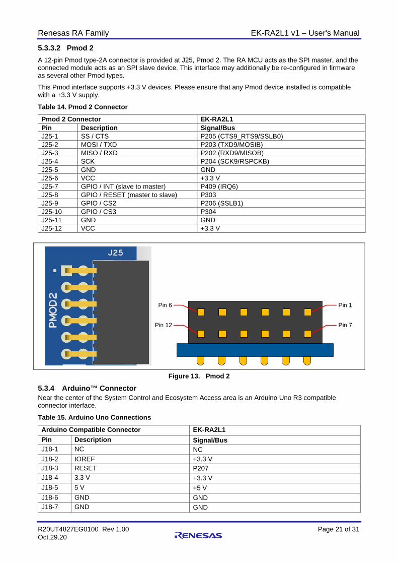
5.3.3.2 Pmod 2 A 12-pin Pmod type-2A connector is provided at J25, Pmod 2. The RA MCU acts as the SPI master, and the connected module acts as an SPI slave device. This interface may additionally be re-configured in firmware as several other Pmod types.
This Pmod interface supports +3.3 V devices. Please ensure that any Pmod device installed is compatible with a +3.3 V supply.
Table 14. Pmod 2 Connector
Pmod 2 Connector EK-RA2L1 Pin Description Signal/Bus J25-1 SS / CTS P205 (CTS9_RTS9/SSLB0) J25-2 MOSI / TXD P203 (TXD9/MOSIB) J25-3 MISO / RXD P202 (RXD9/MISOB) J25-4 SCK P204 (SCK9/RSPCKB) J25-5 GND GND J25-6 VCC +3.3 V J25-7 GPIO / INT (slave to master) P409 (IRQ6) J25-8 GPIO / RESET (master to slave) P303 J25-9 GPIO / CS2 P206 (SSLB1) J25-10 GPIO / CS3 P304 J25-11 GND GND J25-12 VCC +3.3 V
Figure 13. Pmod 2
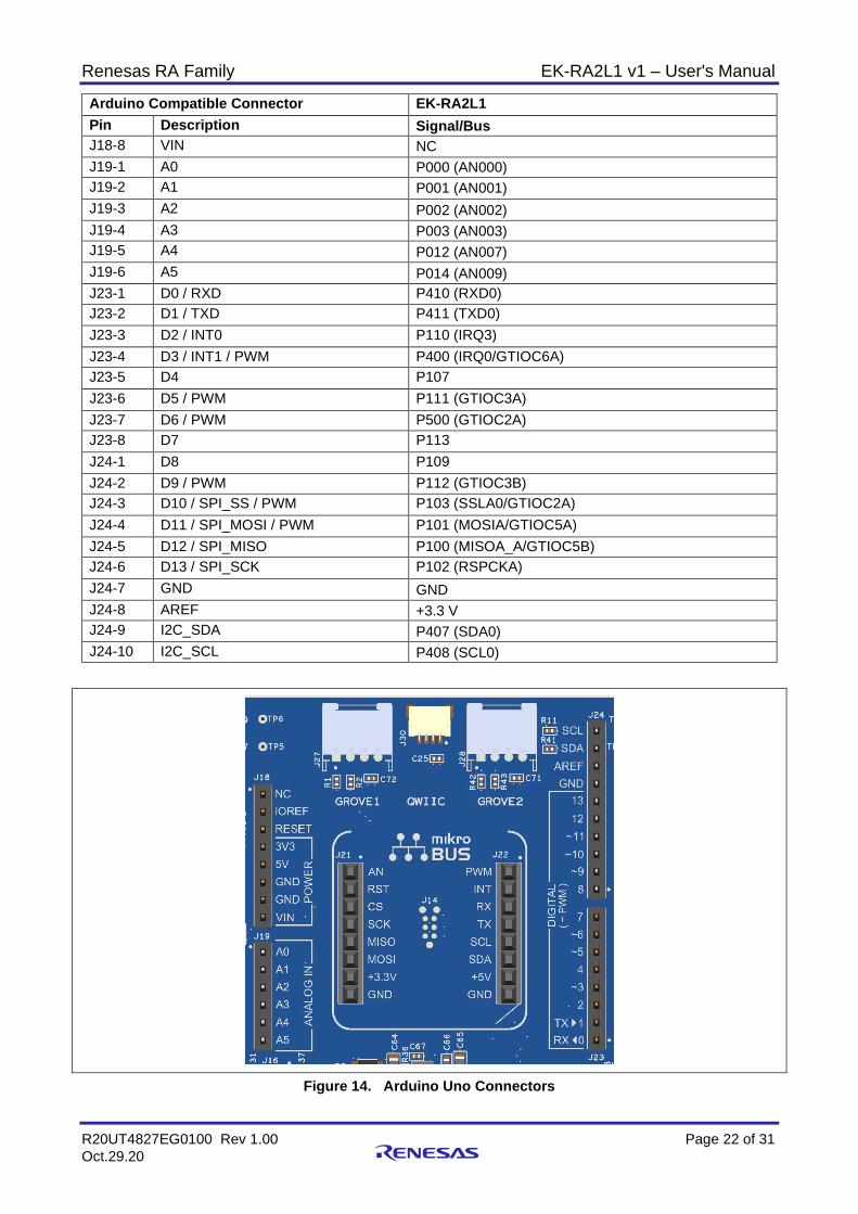
5.3.4 Arduino™ Connector Near the center of the System Control and Ecosystem Access area is an Arduino Uno R3 compatible connector interface.
Table 15. Arduino Uno Connections
Arduino Compatible Connector EK-RA2L1 Pin Description Signal/Bus J18-1 NC NC J18-2 IOREF +3.3 V J18-3 RESET P207 J18-4 3.3 V +3.3 V J18-5 5 V +5 V J18-6 GND GND J18-7 GND GND
Pin 1
Pin 7
Pin 6
Pin 12
Renesas RA Family EK-RA2L1 v1 – User's Manual
R20UT4827EG0100 Rev 1.00 Page 22 of 31 Oct.29.20
Arduino Compatible Connector EK-RA2L1 Pin Description Signal/Bus J18-8 VIN NC J19-1 A0 P000 (AN000) J19-2 A1 P001 (AN001) J19-3 A2 P002 (AN002) J19-4 A3 P003 (AN003) J19-5 A4 P012 (AN007) J19-6 A5 P014 (AN009) J23-1 D0 / RXD P410 (RXD0) J23-2 D1 / TXD P411 (TXD0) J23-3 D2 / INT0 P110 (IRQ3) J23-4 D3 / INT1 / PWM P400 (IRQ0/GTIOC6A) J23-5 D4 P107 J23-6 D5 / PWM P111 (GTIOC3A) J23-7 D6 / PWM P500 (GTIOC2A) J23-8 D7 P113 J24-1 D8 P109 J24-2 D9 / PWM P112 (GTIOC3B) J24-3 D10 / SPI_SS / PWM P103 (SSLA0/GTIOC2A) J24-4 D11 / SPI_MOSI / PWM P101 (MOSIA/GTIOC5A) J24-5 D12 / SPI_MISO P100 (MISOA_A/GTIOC5B) J24-6 D13 / SPI_SCK P102 (RSPCKA) J24-7 GND GND J24-8 AREF +3.3 V J24-9 I2C_SDA P407 (SDA0) J24-10 I2C_SCL P408 (SCL0)
Figure 14. Arduino Uno Connectors
Renesas RA Family EK-RA2L1 v1 – User's Manual
R20UT4827EG0100 Rev 1.00 Page 23 of 31 Oct.29.20
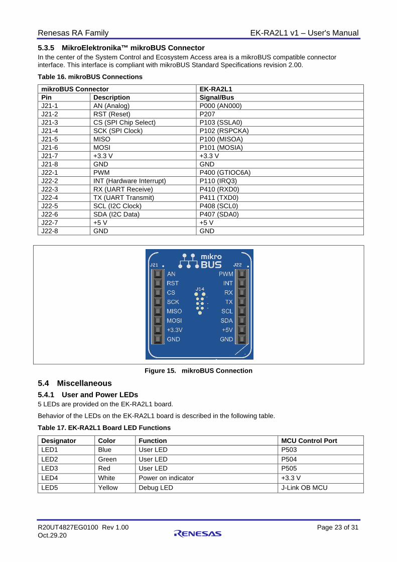
5.3.5 MikroElektronika™ mikroBUS Connector In the center of the System Control and Ecosystem Access area is a mikroBUS compatible connector interface. This interface is compliant with mikroBUS Standard Specifications revision 2.00.
Table 16. mikroBUS Connections
mikroBUS Connector EK-RA2L1 Pin Description Signal/Bus J21-1 AN (Analog) P000 (AN000) J21-2 RST (Reset) P207 J21-3 CS (SPI Chip Select) P103 (SSLA0) J21-4 SCK (SPI Clock) P102 (RSPCKA) J21-5 MISO P100 (MISOA) J21-6 MOSI P101 (MOSIA) J21-7 +3.3 V +3.3 V J21-8 GND GND J22-1 PWM P400 (GTIOC6A) J22-2 INT (Hardware Interrupt) P110 (IRQ3) J22-3 RX (UART Receive) P410 (RXD0) J22-4 TX (UART Transmit) P411 (TXD0) J22-5 SCL (I2C Clock) P408 (SCL0) J22-6 SDA (I2C Data) P407 (SDA0) J22-7 +5 V +5 V J22-8 GND GND
Figure 15. mikroBUS Connection
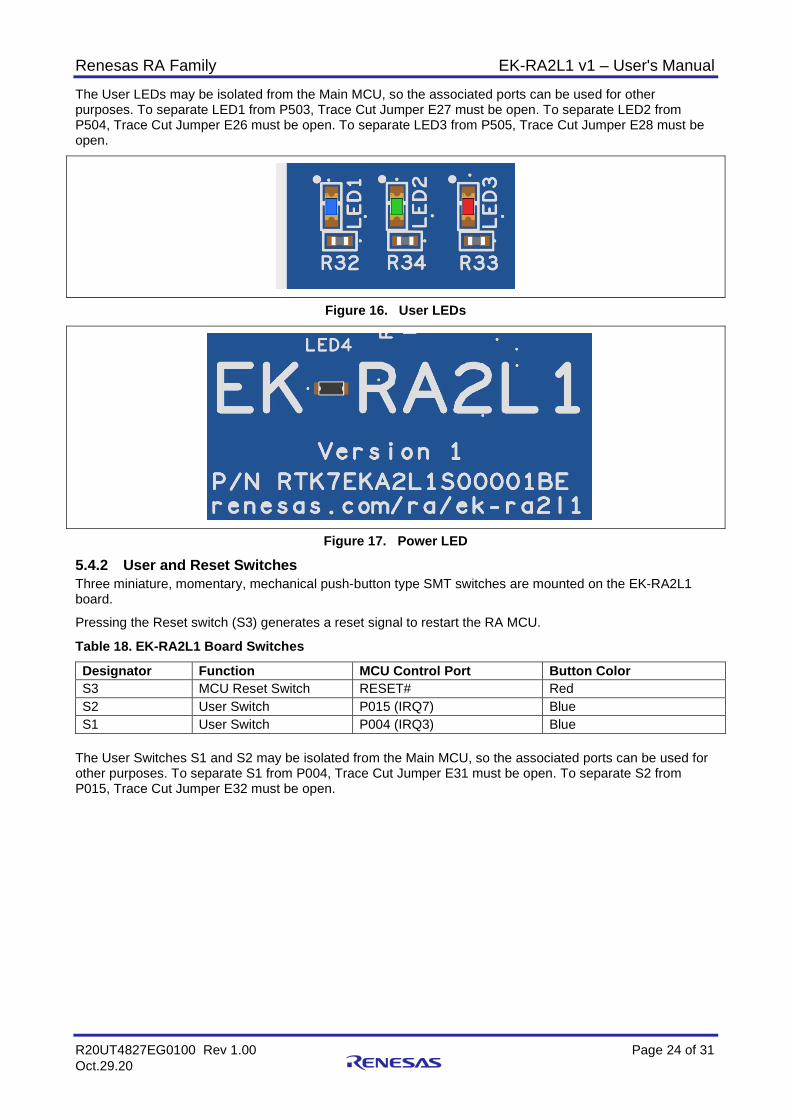
5.4 Miscellaneous 5.4.1 User and Power LEDs 5 LEDs are provided on the EK-RA2L1 board.
Behavior of the LEDs on the EK-RA2L1 board is described in the following table.
Table 17. EK-RA2L1 Board LED Functions
Designator Color Function MCU Control Port LED1 Blue User LED P503 LED2 Green User LED P504 LED3 Red User LED P505 LED4 White Power on indicator +3.3 V LED5 Yellow Debug LED J-Link OB MCU
Renesas RA Family EK-RA2L1 v1 – User's Manual
R20UT4827EG0100 Rev 1.00 Page 24 of 31 Oct.29.20
The User LEDs may be isolated from the Main MCU, so the associated ports can be used for other purposes. To separate LED1 from P503, Trace Cut Jumper E27 must be open. To separate LED2 from P504, Trace Cut Jumper E26 must be open. To separate LED3 from P505, Trace Cut Jumper E28 must be open.
Figure 16. User LEDs
Figure 17. Power LED
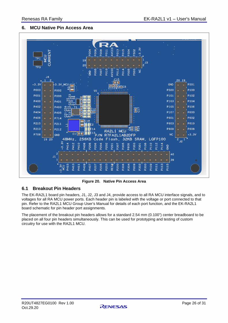
5.4.2 User and Reset Switches Three miniature, momentary, mechanical push-button type SMT switches are mounted on the EK-RA2L1 board.
Pressing the Reset switch (S3) generates a reset signal to restart the RA MCU.
Table 18. EK-RA2L1 Board Switches
Designator Function MCU Control Port Button Color S3 MCU Reset Switch RESET# Red S2 User Switch P015 (IRQ7) Blue S1 User Switch P004 (IRQ3) Blue
The User Switches S1 and S2 may be isolated from the Main MCU, so the associated ports can be used for other purposes. To separate S1 from P004, Trace Cut Jumper E31 must be open. To separate S2 from P015, Trace Cut Jumper E32 must be open.
Renesas RA Family EK-RA2L1 v1 – User's Manual
R20UT4827EG0100 Rev 1.00 Page 25 of 31 Oct.29.20
Figure 18. Reset and User Switches
5.4.3 MCU Boot Mode A two-pin header (J16) is provided to select the Boot mode (P201) of the RA MCU. For normal operation, or Single-Chip mode, leave J16 open. To enter SCI Boot mode or USB Boot mode, place a jumper on J16.
Figure 19. Boot Mode Note: The RA MCU fitted to the EK-RA4M2 board may not contain the latest version of the on-chip boot
firmware.
Renesas RA Family EK-RA2L1 v1 – User's Manual
R20UT4827EG0100 Rev 1.00 Page 26 of 31 Oct.29.20
6. MCU Native Pin Access Area
Figure 20. Native Pin Access Area
6.1 Breakout Pin Headers The EK-RA2L1 board pin headers, J1, J2, J3 and J4, provide access to all RA MCU interface signals, and to voltages for all RA MCU power ports. Each header pin is labeled with the voltage or port connected to that pin. Refer to the RA2L1 MCU Group User’s Manual for details of each port function, and the EK-RA2L1 board schematic for pin header port assignments.
The placement of the breakout pin headers allows for a standard 2.54 mm (0.100”) center breadboard to be placed on all four pin headers simultaneously. This can be used for prototyping and testing of custom circuitry for use with the RA2L1 MCU.
Renesas RA Family EK-RA2L1 v1 – User's Manual
R20UT4827EG0100 Rev 1.00 Page 27 of 31 Oct.29.20
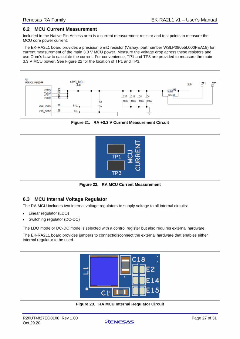
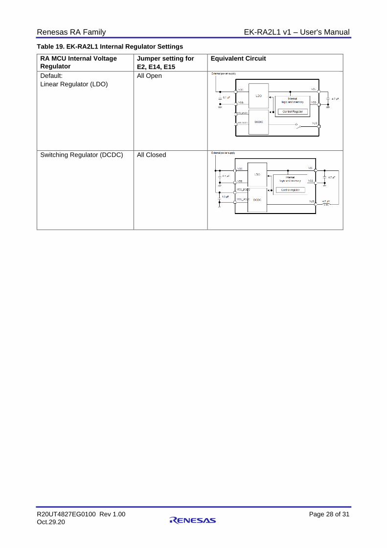
6.2 MCU Current Measurement Included in the Native Pin Access area is a current measurement resistor and test points to measure the MCU core power current.
The EK-RA2L1 board provides a precision 5 mΩ resistor (Vishay, part number WSLP08055L000FEA18) for current measurement of the main 3.3 V MCU power. Measure the voltage drop across these resistors and use Ohm’s Law to calculate the current. For convenience, TP1 and TP3 are provided to measure the main 3.3 V MCU power. See Figure 22 for the location of TP1 and TP3.
Figure 21. RA +3.3 V Current Measurement Circuit
Figure 22. RA MCU Current Measurement
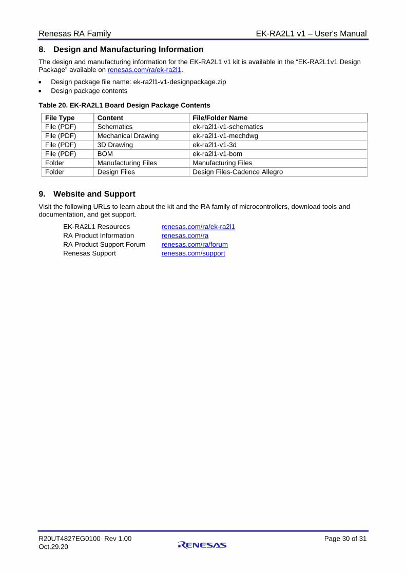
6.3 MCU Internal Voltage Regulator The RA MCU includes two internal voltage regulators to supply voltage to all internal circuits:
• Linear regulator (LDO) • Switching regulator (DC-DC) The LDO mode or DC-DC mode is selected with a control register but also requires external hardware.
The EK-RA2L1 board provides jumpers to connect/disconnect the external hardware that enables either internal regulator to be used.
Figure 23. RA MCU Internal Regulator Circuit
Renesas RA Family EK-RA2L1 v1 – User's Manual
R20UT4827EG0100 Rev 1.00 Page 28 of 31 Oct.29.20
Table 19. EK-RA2L1 Internal Regulator Settings
RA MCU Internal Voltage Regulator
Jumper setting for E2, E14, E15
Equivalent Circuit
Default: Linear Regulator (LDO)
All Open
Switching Regulator (DCDC) All Closed

Renesas RA Family EK-RA2L1 v1 – User's Manual
R20UT4827EG0100 Rev 1.00 Page 29 of 31 Oct.29.20
7. Certifications The EK-RA2L1 v1 kit meets the following certifications/standards. See page 3 of this user’s manual for the disclaimer and precautions.
7.1 EMC/EMI Standards • FCC Notice (Class A)
This device complies with part 15 of the FCC Rules. Operation is subject to the following two conditions: (1) This device may not cause harmful interference, and (2) this device must accept any interference received, including interference that may cause undesired operation.
NOTE- This equipment has been tested and found to comply with the limits for a Class A digital device, pursuant to Part 15 of the FCC Rules. These limits are designed to provide reasonable protection against harmful interference in a residential installation. This equipment generates, uses and can radiate radio frequency energy and, if not installed and used in accordance with the instructions, may cause harmful interference to radio communications. However, there is no guarantee that interference will not occur in a particular installation. If this equipment does cause harmful interference to radio or television reception, which can be determined by turning the equipment off and on, the user is encouraged to try to correct the interference by one or more of the following measures: Reorient or relocate the receiving antenna. Increase the separation between the equipment and receiver. Connect the equipment into an outlet on a circuit different from that to which the receiver is connected. Consult the dealer or an experienced radio/television technician for help.
• Innovation, Science and Economic Development Canada ICES-003 Compliance: CAN ICES-3 (A)/NMB-3(A)
• CE Class A (EMC) This product is herewith confirmed to comply with the requirements set out in the Council Directives on the Approximation of the laws of the Member States relating to Electromagnetic Compatibility Directive 2014/30/EU.
Warning – This is a Class A product. In a domestic environment this product may cause radio interference in which case the user may be required to take adequate measures to correct this interference.
• Taiwan: Chinese National Standard 13438, C6357 compliance, Class A limits • Australia/New Zealand AS/NZS CISPR 32:2015, Class A 7.2 Material Selection, Waste, Recycling and Disposal Standards • EU RoHS • China SJ/T 113642014, 10-year environmental protection use period. 7.3 Safety Standards • UL 94V-0
Renesas RA Family EK-RA2L1 v1 – User's Manual
R20UT4827EG0100 Rev 1.00 Page 30 of 31 Oct.29.20
8. Design and Manufacturing Information The design and manufacturing information for the EK-RA2L1 v1 kit is available in the “EK-RA2L1v1 Design Package” available on renesas.com/ra/ek-ra2l1.
• Design package file name: ek-ra2l1-v1-designpackage.zip • Design package contents Table 20. EK-RA2L1 Board Design Package Contents
File Type Content File/Folder Name File (PDF) Schematics ek-ra2l1-v1-schematics File (PDF) Mechanical Drawing ek-ra2l1-v1-mechdwg File (PDF) 3D Drawing ek-ra2l1-v1-3d File (PDF) BOM ek-ra2l1-v1-bom Folder Manufacturing Files Manufacturing Files Folder Design Files Design Files-Cadence Allegro
9. Website and Support Visit the following URLs to learn about the kit and the RA family of microcontrollers, download tools and documentation, and get support.
EK-RA2L1 Resources renesas.com/ra/ek-ra2l1 RA Product Information renesas.com/ra RA Product Support Forum renesas.com/ra/forum Renesas Support renesas.com/support
Renesas RA Family EK-RA2L1 v1 – User's Manual
R20UT4827EG0100 Rev 1.00 Page 31 of 31 Oct.29.20
Revision History
Rev. Date Description Page Summary
1.00 Oct.29.20 — Initial release

EK-RA2L1 v1 – User’s Manual Publication Date: Oct.29.20 Published by: Renesas Electronics Corporation
R20UT4827EG0100
EK-RA2L1 v1 – User’s Manual