Embed Size (px)
Citation preview
Eindhoven University of Technology
MASTER
A LonTalk protocol interface
implementation in IDaSS
van Loo, T.J.H.
Award date:2000
DisclaimerThis document contains a student thesis (bachelor's or master's), as authored by a student at Eindhoven University of Technology. Studenttheses are made available in the TU/e repository upon obtaining the required degree. The grade received is not published on the documentas presented in the repository. The required complexity or quality of research of student theses may vary by program, and the requiredminimum study period may vary in duration.
General rightsCopyright and moral rights for the publications made accessible in the public portal are retained by the authors and/or other copyright ownersand it is a condition of accessing publications that users recognise and abide by the legal requirements associated with these rights.
• Users may download and print one copy of any publication from the public portal for the purpose of private study or research. • You may not further distribute the material or use it for any profit-making activity or commercial gain
Take down policyIf you believe that this document breaches copyright please contact us providing details, and we will remove access to the work immediatelyand investigate your claim.
Download date: 03. May. 2018
Master's Thesis
Coach: Supervisor: Date:
T U I e lechnische unive!siteil eindhoven
Section of Information and Communication Systems (ICStES) Faculty of Electrical Engineering
ICstEB 735
A LONT ALK PROTOCOL INTERFACE
Implementation in IDaSS
T.J.H. Van Loo
Dr. ir. A.C. Verschueren prof.ir. M.P.J. Stevens January 2000
The Faculty of Electrical Engineering of the Eindhoven University of Technology does not accept any responsibility regarding the contents of Master's Theses

Preface At the end of the education, resulting in the title of "Master of Science in Electrical Engineering" at the Eindhoven University of Technology, students have to work on a final project and report about it in a Master's Thesis. This is such a thesis of a project performed at the section of Information and Communication Systems at the earlier mentioned university. A literature investigation about LonTalk implementations and a LonTalk protocol controller had to be implemented in IDaSS as far as it is sensible to do this in hardware. This report can be seen as a User's Documentation as well.
2

Abstract
LonWorks, a registered trademark of Echelon Corporation, is a technology to build distributed control systems and products. Lon stands for Local Operating Networks. It provides a solution to the many problems of designing, building, installing, and maintaining control networks.
The purpose of this thesis is to describe an implementation of a LonTalk Protocol interface to the microcontroller in IOaSS. IOaSS [Verschueren] stands for Interactive Design and Simulation System.
The project is started with collecting information about the LonTalk protocol. The most important conclusion that follows from the literature survey is that there is much literature about applications of the Lon protocol, but not much literature about the exact working or an implementation.
With the available information, a description of the LonTalk Protocol is given, for so far it is important to know for implementing the protocol in Hardware.
Next, the design is started from the communication medium side and divided in functional blocks that are as basic as possible. These primary blocks are combined in three units: the Medium Interface Unit, the Codec and Converter Unit and the Processor Interface Unit. In three chapters, the functionality, conditions and protocol descriptions of each unit are described.
Then, the way of testing these units and its results are presented. In the last chapters, the interface to microcontroller is explained.
Finally an example of the use of the designed LonTalk Interface Unit is given. In this example, many things are presented in a general way, leaving the exact implementation open.
3
Contents
Preface
Abstract
Contents
1 Introduction
2 LonTalk protocol description
3 The Medium Interface Unit
3.1 Introduction
3.2 The receiving part of the Medium Interface Unit 3.2.1 The Input Buffers 3.2.2 The Transition Detect units 3.2.3 The Phase Lock Loop 3.2.4 The Idle and Bit detector
3.3 The transmitting part of the Medium Interface Unit 3.3.1 The Manchester Encoder 3.3.2 The AddSync module
3.4 The Collision Detector
3.5 Multiplexing in the Medium Interface Unit
4 The Codec and Convert unit
4.1 Introduction
4.2 The CRC Encoder and Byte-to-Bit converter
4.3 The CRC Decoder and the Bit-to-Byte converter
5 The Processor Interface Unit
5.1 Introduction
5.2 The Register Selector
5.3 The Port Controller 5.3.1 The transmit side 5.3.2 The receive side 5.3.3 Error handling and control
6 Testing
2
3
4
6
8
11
11
14 14 15 16 19
21 21 23
25
28
30
30
32
34
37
37
38
40 40 41 42
45
4
6.1 Introduction 45
6.2 The bit stream generator 45
6.3 Test of the receiving units of the Medium Interface Unit. 46
6.4 Test of the sending part and the receiving part of Medium Interface Unit 48
7 Control of the Interface
7.1 Basic Operations
7.2 A Link layer Protocol interface
7.3 A Link Layer Protocol
8 Conclusions and recommendations
Bibliography
50
50
51
53
59
60
5
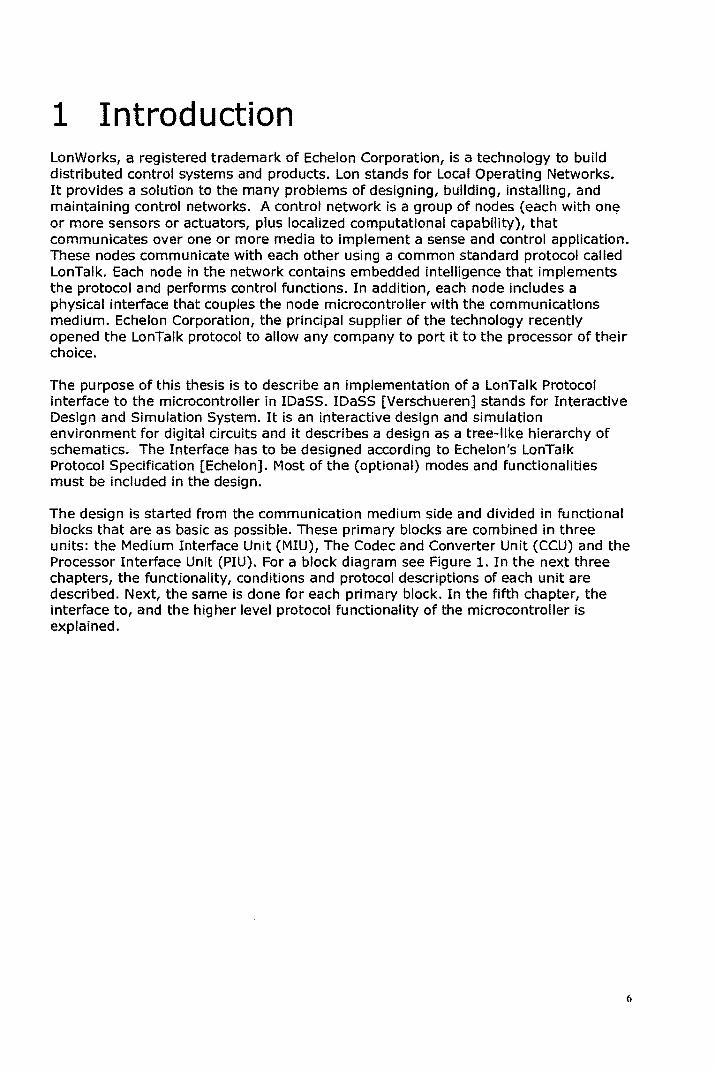
1 Introduction LonWorks, a registered trademark of Echelon Corporation, is a technology to build distributed control systems and products. Lon stands for Local Operating Networks. It provides a solution to the many problems of designing, building, installing, and maintaining control networks. A control network is a group of nodes (each with one or more sensors or actuators, plus localized computational capability), that communicates over one or more media to implement a sense and control application. These nodes communicate with each other using a common standard protocol called LonTalk. Each node in the network contains embedded intelligence that implements the protocol and performs control functions. In addition, each node includes a physical interface that couples the node microcontroller with the communications medium. Echelon Corporation, the principal supplier of the technology recently opened the LonTalk protocol to allow any company to port it to the processor of their choice.
The purpose of this thesis is to describe an implementation of a LonTalk Protocol interface to the microcontroller in IDaSS. IDaSS [Verschueren] stands for Interactive Design and Simulation System. It is an interactive design and simulation environment for digital circuits and it describes a design as a tree-like hierarchy of schematics. The Interface has to be designed according to Echelon's LonTalk Protocol Specification [Echelon]. Most of the (optional) modes and functionalities must be included in the design.
The design is started from the communication medium side and divided in functional blocks that are as basic as possible. These primary blocks are combined in three units: the Medium Interface Unit (MIU), The Codec and Converter Unit (CCU) and the Processor Interface Unit (PIU). For a block diagram see Figure 1. In the next three chapters, the functionality, conditions and protocol descriptions of each unit are described. Next, the same is done for each primary block. In the fifth chapter, the interface to, and the higher level protocol functionality of the microcontroller is explained.
6

rO"'r:':" ~:::::::,:::,:o:-::':::·::::~'::::B·:::::'::'::·::'::::·:::=-::·::·:: ~:-:':~i-::: ,::-::':-::'=-:':="l-', ! : INT Dout Din SEL Rd Wr Ai j l i : '114 i I A I! } ! : Register Selector \r!-hJ !: Rate Setting Data DT A CMD Error Statu DRA Data IN 1! I r
">- ~ ">-
~/" ~7 ", I
/ Data DT A CMD Error Statu DRA Data IN: ....... Echo :. ,.. Port Controller
I : Pl bcesso / r-I" M~~;a TBC ServReq EOP Abort Coli Val Coli RBC DataR Idle! ! ~ : It erface • ~ i I U it A II- ~ I. ~~ < ~ ~!l>: i i L_ ---- --- - _ ---- ---- _ _ ______ -- ----____ _J j
I !-~~ u------~, --~;--- -------- -1 i I 1 DataT TBC ServR EOF Abofl RBC DataR : !
;,' i.I ____ ~_~!;~t:~:d. Um! D-:~ and ~~Ck ~~ _ .. I :l! .... _____ ~qg.!l~!!r..!tc.Q.l\Y!<I!i.!.lg!.! i!: ______________________ _
I c--- --- --- -- -------- --- -- ---------------- -------- ---- -------- -, I
II ~? ~N':::ruk D~~::;~ _rl.ce :::&0011 V::R:: ::: II i : Medium Interface Unit ,~ A II- A II- II- A!L : i L,::.::,:.~.~ .. :.::.:.::__::.~_:.:~ .. :.::.::.:.:.:.::: .................... ,. .. ~ .. :.:.~.=.~.:.:.::.:::.:::.:: ... :.: .. :.:.:.::.:.:,::: .. :.:.:.: ... -------: .... :-.:.: . .J
" Figure 1,:LonTalk Interface
7
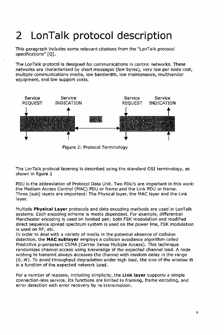
2 LonTalk protocol description This paragraph includes some relevant citations from the "LonTalk protocol specifications" [Q].
The LonTalk protocol is designed for communications in control networks. These networks are characterized by short messages (few bytes), very low per node cost, multiple communications media, low bandwidth, low maintenance, multivendor equipment, and low support costs.
Service REQUEST
Service INDICATION
Service Service REQUEST INDICATION
Figure 2: Protocol Terminology
The LonTalk protocol layering is described using the standard OSI terminology, as shown in figure 2
PDU is the abbreviation of Protocol Data Unit. Two PDU's are important in this work: the Medium Access Control (MAC) PDU or frame and the Link PDU or frame. Three (sub) layers are important: The Physical layer, the MAC layer and the Link layer.
Multiple Physical Layer protocols and data encoding methods are used in LonTalk systems. Each encoding scheme is media dependent. For example, differential Manchester encoding is used on twisted pair, both FSK modulation and modified direct sequence spread spectrum system is used on the power line, FSK modulation is used on RF, etc. In order to deal with a variety of media in the potential absence of collision detection, the MAC sublayer employs a collision avoidance algorithm called Predictive p-persistent CSMA (Carrier Sense Multiple Access). This technique randomizes channel access using knowledge of the expected channel load. A node wishing to transmit always accesses the channel with random delay in the range (O .. W). To avoid throughput degradation under high load, the size of the window W is a function of the expected network load.
For a number of reasons, including simplicity, the Link layer supports a simple connection-less service. Its functions are limited to framing, frame encoding, and error detection with error recovery by re-transmission.
8
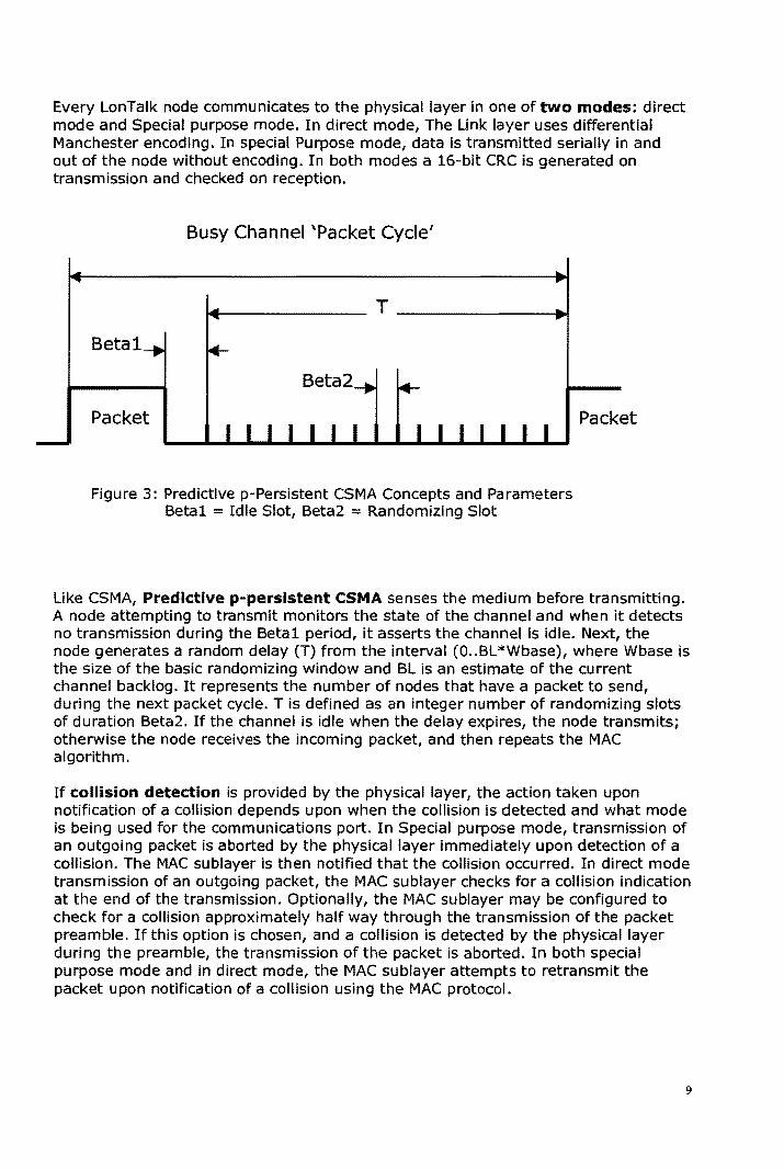
Every LonTalk node communicates to the physical layer in one of two modes: direct mode and Special purpose mode. In direct mode, The Link layer uses differential Manchester encoding. In special Purpose mode, data is transmitted serially in and out of the node without encoding. In both modes a 16-bit CRC is generated on transmission and checked on reception.
Busy Channel 'Packet Cycle'
~_____________ T ______________ ~
Beta 1
Beta2
Packet
Figure 3: Predictive p-Persistent CSMA Concepts and Parameters Betal = Idle Slot, Beta2 = Randomizing Slot
Packet
Like CSMA, Predictive p-persistent CSMA senses the medium before transmitting. A node attempting to transmit monitors the state of the channel and when it detects no transmission during the Betal period, it asserts the channel is idle. Next, the node generates a random delay (T) from the interval (O .. BL*Wbase), where Wbase is the size of the basic randomizing window and BL is an estimate of the current channel backlog. It represents the number of nodes that have a packet to send, during the next packet cycle. T is defined as an integer number of randomizing slots of duration Beta2. If the channel is idle when the delay expires, the node transmits; otherwise the node receives the incoming packet, and then repeats the MAC algorithm.
If collision detection is provided by the physical layer, the action taken upon notification of a collision depends upon when the collision is detected and what mode is being used for the communications port. In Special purpose mode, transmission of an outgoing packet is aborted by the physical layer immediately upon detection of a collision. The MAC sublayer is then notified that the collision occurred. In direct mode transmission of an outgoing packet, the MAC sublayer checks for a colliSion indication at the end of the transmission. Optionally, the MAC sublayer may be configured to check for a collision approximately half way through the transmission of the packet preamble. If this option is chosen, and a collision is detected by the physical layer during the preamble, the transmission of the packet is aborted. In both special purpose mode and in direct mode, the MAC sublayer attempts to retransmit the packet upon notification of a collision using the MAC protocol.
9
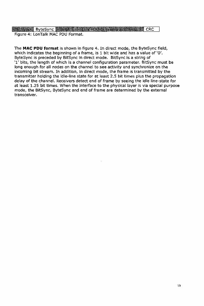
Figure 4: LonTalk MAC PDU Format.
The MAC PDU format is shown in figure 4. In direct mode, the ByteSync field, which indicates the beginning of a frame, is 1 bit wide and has a value of '0'. ByteSync is preceded by BitSync in direct mode. BitSync is a string of '1' bits, the length of which is a channel configuration parameter. BitSync must be long enough for all nodes on the channel to see activity and synchronize on the incoming bit stream. In addition, in direct mode, the frame is transmitted by the transmitter holding the idle-line state for at least 2.5 bit times plus the propagation delay of the channel. Receivers detect end of frame by seeing the idle line-state for at least 1.25 bit times. When the interface to the physical layer is via special purpose mode, the BitSync, ByteSync and end of frame are determined by the external transceiver.
10
3 The Medium Interface Unit
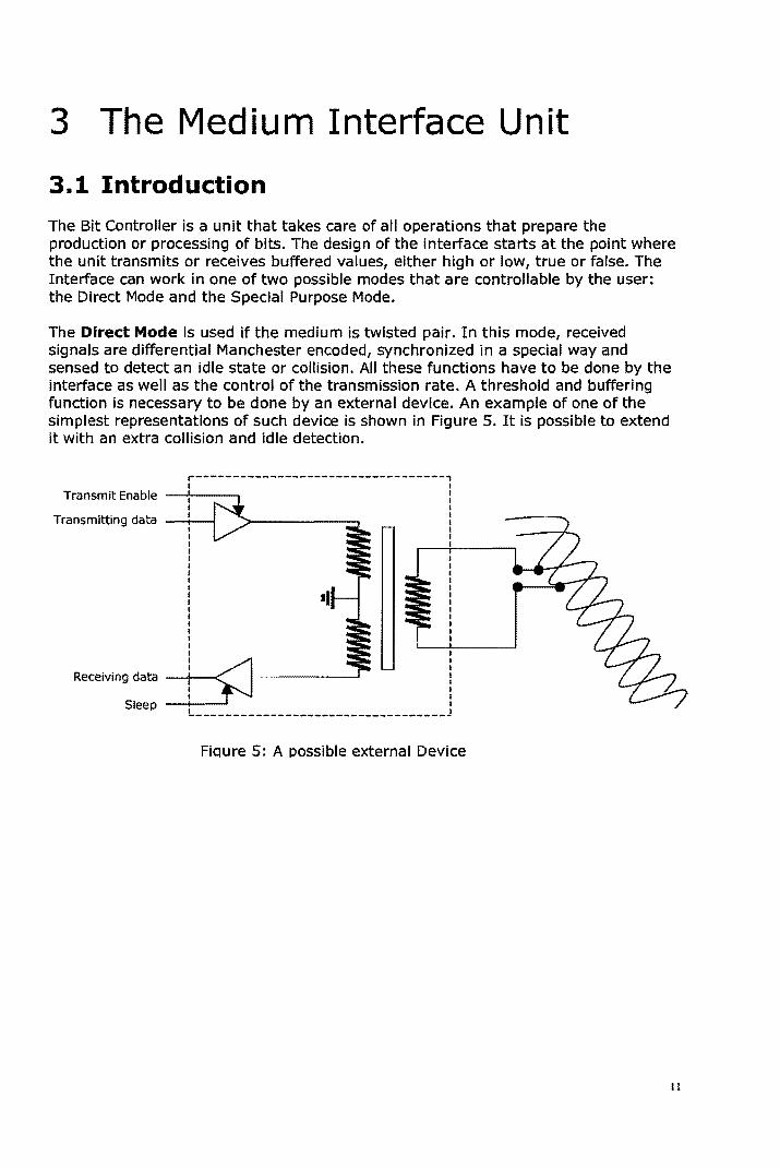
3.1 Introduction The Bit Controller is a unit that takes care of all operations that prepare the production or processing of bits. The design of the interface starts at the point where the unit transmits or receives buffered values, either high or low, true or false. The Interface can work in one of two possible modes that are controllable by the user: the Direct Mode and the Special Purpose Mode.
The Direct Mode is used if the medium is twisted pair. In this mode, received signals are differential Manchester encoded, synchronized in a special way and sensed to detect an idle state or collision. All these functions have to be done by the interface as well as the control of the transmission rate. A threshold and buffering function is necessary to be done by an external device. An example of one of the simplest representations of such device is shown in Figure S. It is possible to extend it with an extra collision and idle detection.
r----------------------------------, I I Transmit Enable -+----, :
I
Transmitting data : I I I
Receiving data -+--< I I I I
Sleep -----' I L __________________________________ l
Fiqure 5: A possible external Device
It
For this mode, the functional blocks of the Bit Controller are presented in Figure 6. At the transmitting side, we find a Manchester encoder, preceded by a unit that adds a synchronization stream to the front of the frame to transmit. At the receiving side we find a transition detector, a phase locked loop (PLL) and a unit that handles the Idle detection, the Manchester decoding and a Bit synchronization mechanism. The Collision detector compares the data leaving at the transmitting side and the delayed data coming from the receiving side. In the next paragraphs, these basic blocks will be described.
r- - -- - -----I I I I I I I I I I I I I I I
Rate
-6mi- Serr-- Da~--- -----Req Req
Add Mode Synchro bits
Manch.Enc CLK
<::(;11------------- --- --Valid
Collision
Detector
Input Buffers
------ -, Sleep I
I , I I I I
, I I I I I I I I I I I I I I I I I I I I
I TE DTX ColI.Det DRX Sleep: L _________________ _ ______________________ ________________________ __________ _J
Figure 6: The Medium Interface Unit in Direct Mode.
The Special Purpose Mode is used for all other kinds of medium. In this mode, encoding, synchronization and monitoring the medium for a collision or an idle state must be done by an external device. The transmission rate is controlled by the external device as well. For this mode, the functional blocks of the Bit Controller are presented in Figure 7. Both at the transmitting side and at the receiving side we find a transition detector on the receiving clock signals. The collision detector compares the data leaving at the transmitting side and the delayed data coming from the receiving side. In the next paragraphs, these basic blocks will be described.
12
.h ~ ~ .. Ail- J~ ~ .. r--------------I
----- se;v-- oiiia--- ----- fo'iC ----- (:011------------- --- --Data Req Req Valid
.. TAl"
MO~ ... ~ Vain .. ... .. "6' ...
Data ... ~ Collision
Valid .. ~
CLK .. Detector ~
Trans. Trans. Detect Detect
J~ A~ A
Col1.Det. Input Buffers
I I I I I I I I I I I I I I I I I I I I I I I I I I I I I I I I I I I I I I I I I I I I I I DTX
TR Req CLKT CLKR DR~ ~ Idl L _____________ _
----- ----- ------------------ -------------------- --- -- -U U
Figure 7: The Medium Interface Unit in Special Purpos Mode.
--S~p -1 I I t I I I I I I I I I I I I I I I I I I I I I I I I I I I I I I I I I I I I I I I I I
Sleep : _J
The actual implementation is a multiplexed version of both schematics. In this way, it is possible to provide two modes and only a few pins at the medium side. The next table shows the way the signals are multiplexed. The column indicating 'Pin' represents the pin number on the Echelon Neuron Chip.
Pin Direct Mode Special Purpose Mode 1 Data Transmit (DTX) Data Transmit (DTX) 2 Data Receive (DRX) Data Receive (DRX) 3 Sleep Sleep 4 Collision Detect Collision Detect 5 Transmit Enable (TE) Transmission Request 6 Not Connected Idle External 7 Not Connected Tra nsmit Clock (TCLK) 8 Not Connected Receive Clock (RCLK)
13
3.2 The receiving part of the Medium Interface Unit
The design is started with the receiving part of the Medium Interface Unit. In Direct Mode, one input signal 'Data Receive eXternal' (DRX) is received. This input signal is unsynchronized with the system clock and therefore, the input signal is lead through an input buffer first. Next, the transitions in the input signal are detected in the Transition detector and fed to a unit called the Phase Lock Loop. Here a receive clock signal is generated. Finally follows the Idle and Bit detector It determines the synchronization bits end bytes at the beginning of a packet, the bit values and the idle condition of the line.
3.2.1 The Input Buffers
The Input from the line is unstable and unsynchronized with the clock signal. By leading it through two buffers, these problems can be solved. The implementation of his unit is formed by two registers that load by default. Each system clock, the actual value of the line is loaded in the first register. The next System clock this value is passed to the next register and the first register loads the value that is on the line now. Figure 8 shows the schematic.
~ [!J DRX III [!J III AI 10 bits II }tJ
Line_In FiI:stBuf LastBuf
Buff_Out
m !REG
Figure 8: The Input Buffers
14
3.2.2 The Transition Detect units
The Transition Detect unit is a unit that detects the transitions of successive bit values. It gives a '1' at each transition and a '0' if there is no transition.
Bit Trans
Figure 9: The flow diagram of the Transition Detect Unit.
The Transition Detect unit consists of a register 'prevValue', an operator 'TransNot' and two off-schematic connectors. The register contains the value of the previous bit. The operator copies the input bit value from the input connector 'Bits' to the register input and it compares the bit value of the input connector with the value of the previous bit which is stored in the register. If they are different, the module returns a '1' at the output connector 'Trans', else it returns a '0'.
The schematic of the transition Detect unit is given in figure 10.
bits I bits t:t:ans
T:t:ansnot ac1::; p:t:ev
I OP
act p:t:ev p:t:evValue
FE
t:t:ans
Figure 10: The schematic of the Transition Detect unit.
15
3.2.3 The Phase Lock Loop
A Phase Lock Loop (PLL) is a unit that extracts a clock signal from its input signal and passes it to the transmitter. The Phase Lock Loop we need is one that can extract a clock signal out of a Manchester coded input signal. The receiving clock signal gives a pulse at each beginning and middle of a bit time. Further more the PLL has to give a signal that contains a value telling whether there was a transition that beginning or middle of a bit time.
The Manchester code that is used in the LonTalk protocol is a differential code. This encoding method has the benefits of zero DC offset, polarity insensitivity, and simple bit synchronization between the transmitter and the receiver(s):
In the Differential Manchester encoding method, there is a minimum of one transition per bit time at the beginning of the bit time. If there is a second transition within the bit time, it occurs in the middle of the bit. By convention, a single transition per bit time is a '1' and two evenly spaced transitions per bit time is a '0'.
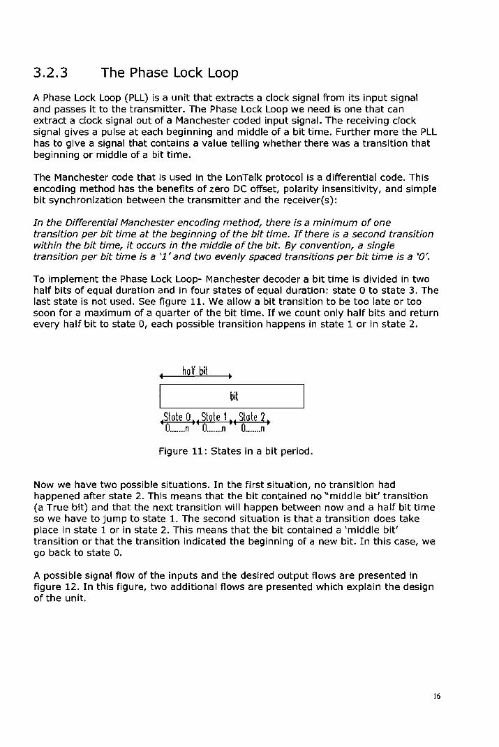
To implement the Phase Lock Loop- Manchester decoder a bit time is divided in two half bits of equal duration and in four states of equal duration: state 0 to state 3. The last state is not used. See figure 11. We allow a bit transition to be too late or too soon for a maximum of a quarter of the bit time. If we count only half bits and return every half bit to state 0, each possible transition happens in state 1 or in state 2.
half bil
bit
4Slole 0 ~ 4 Slole 1 ~ 4 Slole 2 ~ O ••••••• n O ••••••• n O ••••••• n
Figure 11: States in a bit period.
Now we have two possible situations. In the first situation, no transition had happened after state 2. This means that the bit contained no "middle bit' transition (a True bit) and that the next transition will happen between now and a half bit time so we have to jump to state 1. The second situation is that a transition does take place in state 1 or in state 2. This means that the bit contained a 'middle bit' transition or that the transition indicated the beginning of a new bit. In this case, we go back to state o.
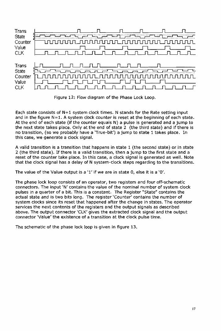
A possible signal flow of the inputs and the desired output flows are presented in figure 12. In this figure, two additional flows are presented which explain the design of the unit.
16
Trans State Counter Value ClK
Trans State Counter Value ClK
Figure 12: Flow diagram of the Phase lock loop.
Each state consists of N+1 system clock times. N stands for the Rate setting input and in the figure N=1. A system clock counter is reset at the beginning of each state. At the end of each state (if the counter equals N) a pulse is generated and a jump to the next state takes place. Only at the end of state 2 (the third state) and if there is no transition, (so we probably have a 'True-bit') a jump to state 1 takes place. In this case, we generate a clock signal.
A valid transition is a transition that happens in state 1 (the second state) or in state 2 (the third state). If there is a valid transition, then a jump to the first state and a reset of the counter take place. In this case, a clock signal is generated as well. Note that the clock signal has a delay of N system-clock steps regarding to the transitions.
The value of the Value output is a '1' if we are in state 0, else it is a '0'.
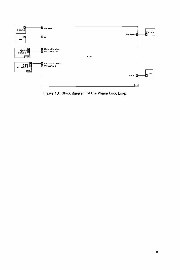
The phase lock loop consists of an operator, two registers and four off-schematic connectors. The input 'N' contains the value of the nominal number of system clock pulses in a quarter of a bit. This is a constant. The Register "State" contains the actual state and is two bits long. The register 'Counter' contains the number of system clocks since its reset that happened after the change in states. The operator services the next contents of the registers and the output signals as described above. The output connector 'ClK' gives the extracted clock signal and the output connector 'Value' the existence of a transition at the clock pulse time.
The schematic of the phase lock loop is given in figure 13.
17
Val.ue ~----llL_-1
i-=-:-:-:-:=-r.iI-----tIa Nex eState
PLL
i--:::-:~liIl_---tIa CouneeJ:New
CLK CLK IIIJ----KJ
OP
Figure 13: Block diagram of the Phase Lock Loop.
18
3.2.4 The Idle and Bit detector
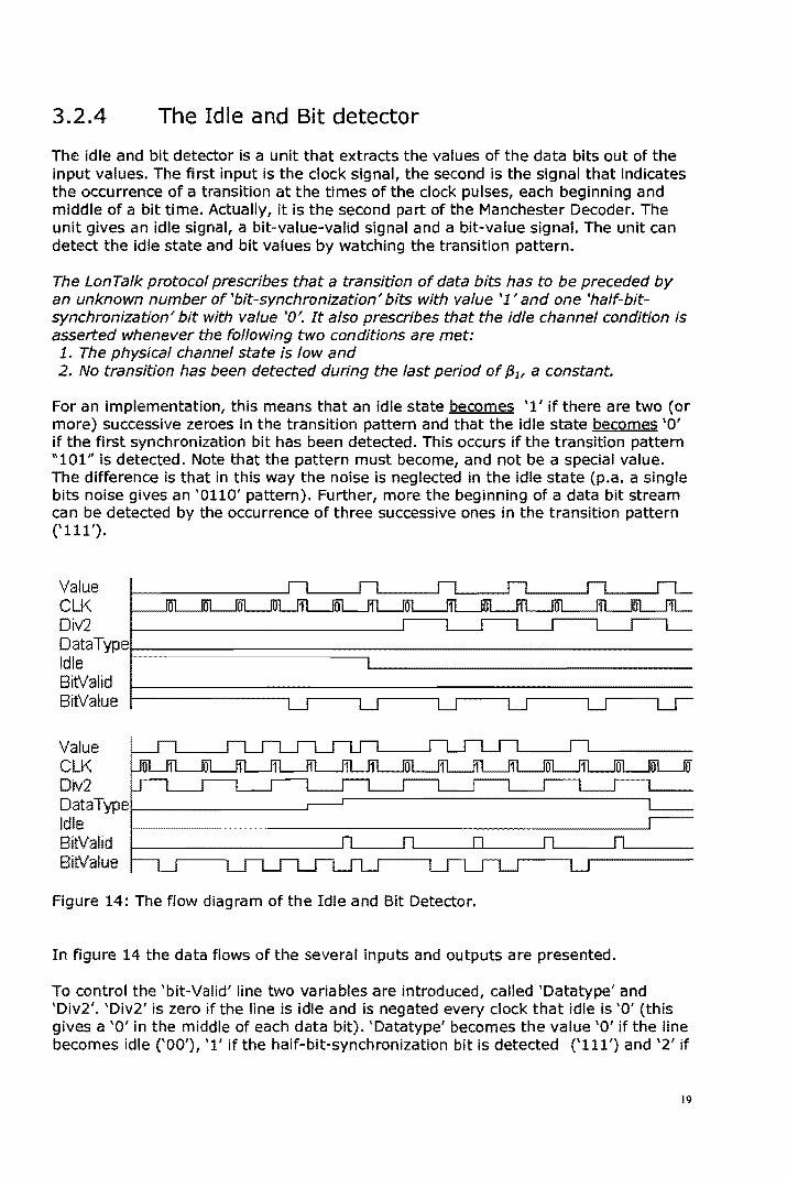
The idle and bit detector is a unit that extracts the values of the data bits out of the input values. The first input is the clock signal, the second is the signal that indicates the occurrence of a transition at the times of the clock pulses, each beginning and middle of a bit time. Actually, it is the second part of the Manchester Decoder. The unit gives an idle signal, a bit-value-valid signal and a bit-value signal. The unit can detect the idle state and bit values by watching the transition pattern.
The LonTalk protocol prescribes that a transition of data bits has to be preceded by an unknown number of 'bit-synchronization' bits with value '1' and one 'half-bitsynchronization' bit with value '0'. It a/so prescribes that the idle channel condition is asserted whenever the following two conditions are met: 1. The physical channel state is low and 2. No transition has been detected during the last period of 131, a constant.
For an implementation, this means that an idle state becomes '1' if there are two (or more) successive zeroes in the transition pattern and that the idle state becomes '0' if the first synchronization bit has been detected. This occurs if the transition pattern "101" is detected. Note that the pattern must become, and not be a special value. The difference is that in this way the noise is neglected in the idle state (p.a. a single bits noise gives an '0110' pattern). Further, more the beginning of a data bit stream can be detected by the occurrence of three successive ones in the transition pattern ('111').
Value ClK Div2 DataTypet==================::::::;:-------------Idle BitValid BitValue
Value ClK Div2 o ataTyp e 1--______ ----'
Idle BitValid BitValue
Figure 14: The flow diagram of the Idle and Bit Detector.
In figure 14 the data flows of the several inputs and outputs are presented.
To control the 'bit-Valid' line two variables are introduced, called 'Datatype' and 'Div2'. 'Div2' is zero if the line is idle and is negated every clock that idle is '0' (this gives a '0' in the middle of each data bit). 'Datatype' becomes the value '0' if the line becomes idle COO'), '1' if the half-bit-synchronization bit is detected ('111') and '2' if
19
the next transition takes place (then there is a real data bit), Only in this last case and if the 'Div2' variable is '0', the 'BitValid' clock can be '1', else'O',
The 'Bitvalue' line gives the negated value of the previous transition and is correct if 'BitValid' is '1',
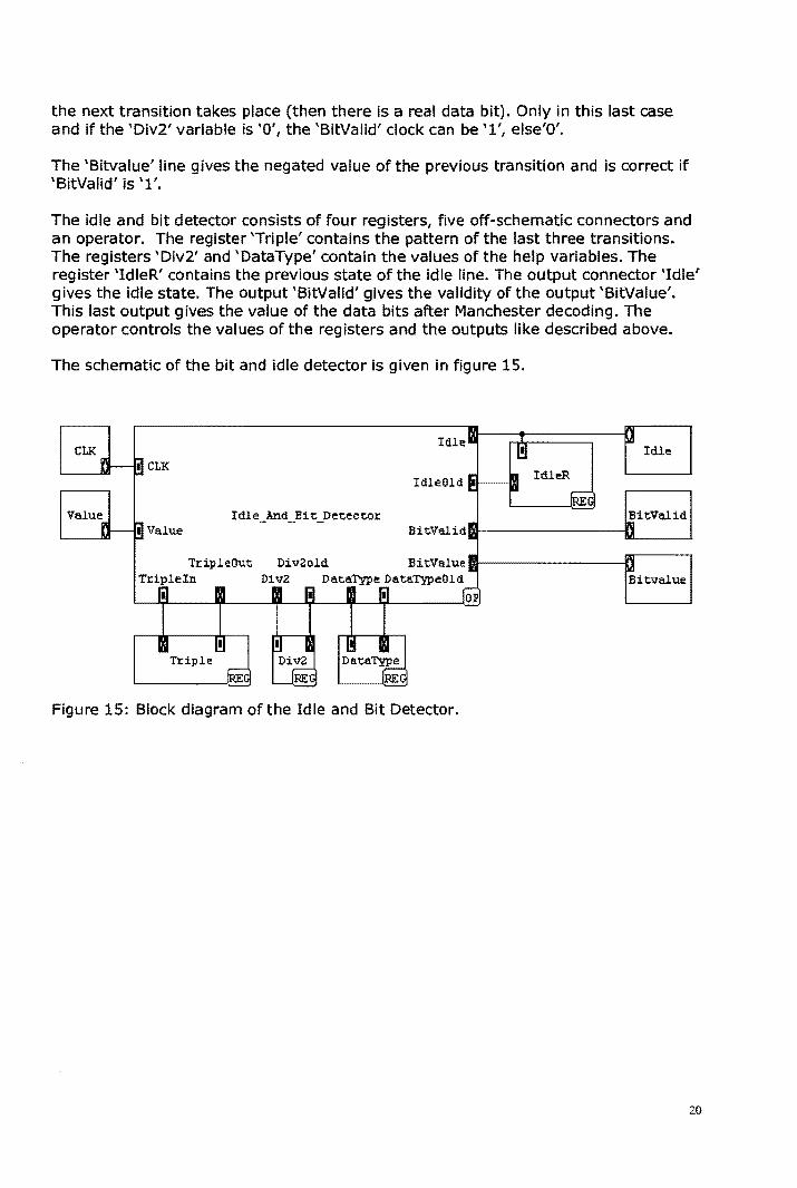
The idle and bit detector consists of four registers, five off-schematic connectors and an operator, The register 'Triple' contains the pattern of the last three tranSitions. The registers 'Div2' and 'DataType' contain the values of the help variables. The register 'IdleR' contains the previous state of the idle line. The output connector 'Idle' gives the idle state. The output 'BitValid' gives the validity of the output 'BitValue'. This last output gives the value of the data bits after Manchester decoding. The operator controls the values of the registers and the outputs like described above.
The schematic of the bit and idle detector is given in figure 15.
eLK Idle
IdleR
BitValid
Div20ld BitValue Ii--------K--"l DataType DataTypeOld Bitvalue
OP
RE
Figure 15: Block diagram of the Id Ie and Bit Detector.
20
3.3 The transmitting part of the Medium Interface Unit
3.3.1 The Manchester Encoder
The Manchester encoder is a unit that converts data bits into a transmittable! Manchester encoded data stream! according to the lonTalk Protocol:
Before beginning to transmit the packet, the output data pin (DTX) has to be initialized to start low. Then the Transmit Enable (TE) pin has to be asserted, which ensures that the first transition in the packet is from low to high. This first transition occurs within 1 bit time of asserting Transmit Enable and marks the beginning of a packet.
The packet has to be terminated by forcing a Differential Manchester Line-code violation; i.e., it holds the data output transitionless long enough for the receiver to recognize an invalid code that signals the end of transmission. The output can be either high or low for the duration of the line-code violation, depending on the state of the data output after transmitting the last bit. The line-code violation lasts for at least 2 bit times. Note that the last bit does not have a trailing clock edge, so the data output actually remains transitionless for at least 2.5 bit times. The Transmit Enable pin is held active until the end of the line-code violation, and is then released.
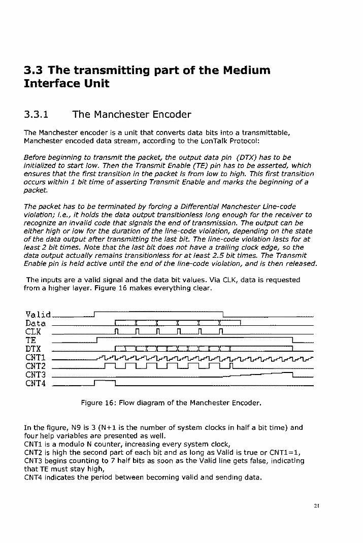
The inputs are a valid signal and the data bit values. Via ClK! data is requested from a higher layer. Figure 16 makes everything clear.
Valid ___ ---I Data ClK TE DTX CNTl CNT2 CNT3 CNT4
Figure 16: Flow diagram of the Manchester Encoder.
In the figure! N9 is 3 (N+1 is the number of system clocks in half a bit time) and four help variables are presented as well. CNT1 is a modulo N counter! increasing every system clock! CNT2 is high the second part of each bit and as long as Valid is true or CNT1=1! CNT3 begins counting to 7 half bits as soon as the Valid line gets false! indicating that TE must stay high! CNT4 indicates the period between becoming valid and sending data.
21
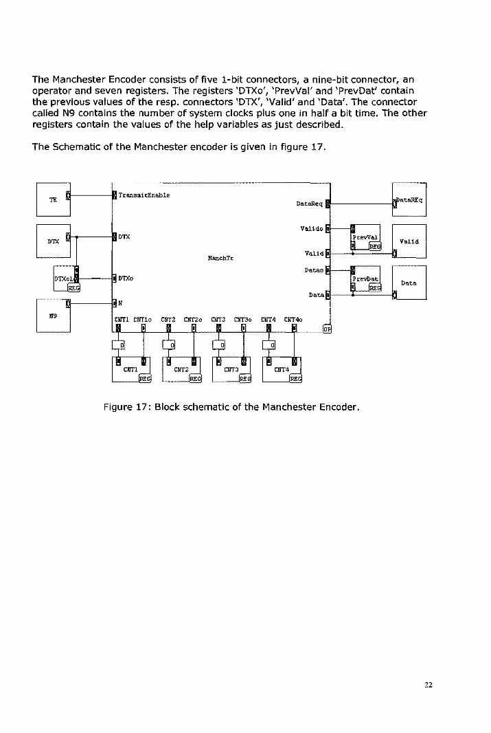
The Manchester Encoder consists of five i-bit connectorsl a nine-bit connector, an operator and seven registers. The registers 'DTXo'/ 'PrevVal' and 'PrevDatl contain the previous values of the resp. connectors 'DTX', 'Valid' and 'Datal. The connector called N9 contains the number of system clocks plus one in half a bit time. The other registers contain the values of the help variables as just described.
The Schematic of the Manchester encoder is given in figure 17.
n-----m TranslIli tEnable M-_____ Irat~q
Valid
Data
Figure 17: Block schematic of the Manchester Encoder.
22
3.3.2 The AddSync module
The AddSync module is a unit that adds a synchronization preamble at the beginning of a packet according to the LonTalk protocol.
The preamble consists of a bit-sync field and a byte-sync field. The bit-sync field is a series of 1 's; its duration is a user selectable and is at least six bits long. The Bytesync field is a single bit 0 that marks the end of the preamble, and the beginning of the first byte of the packet.
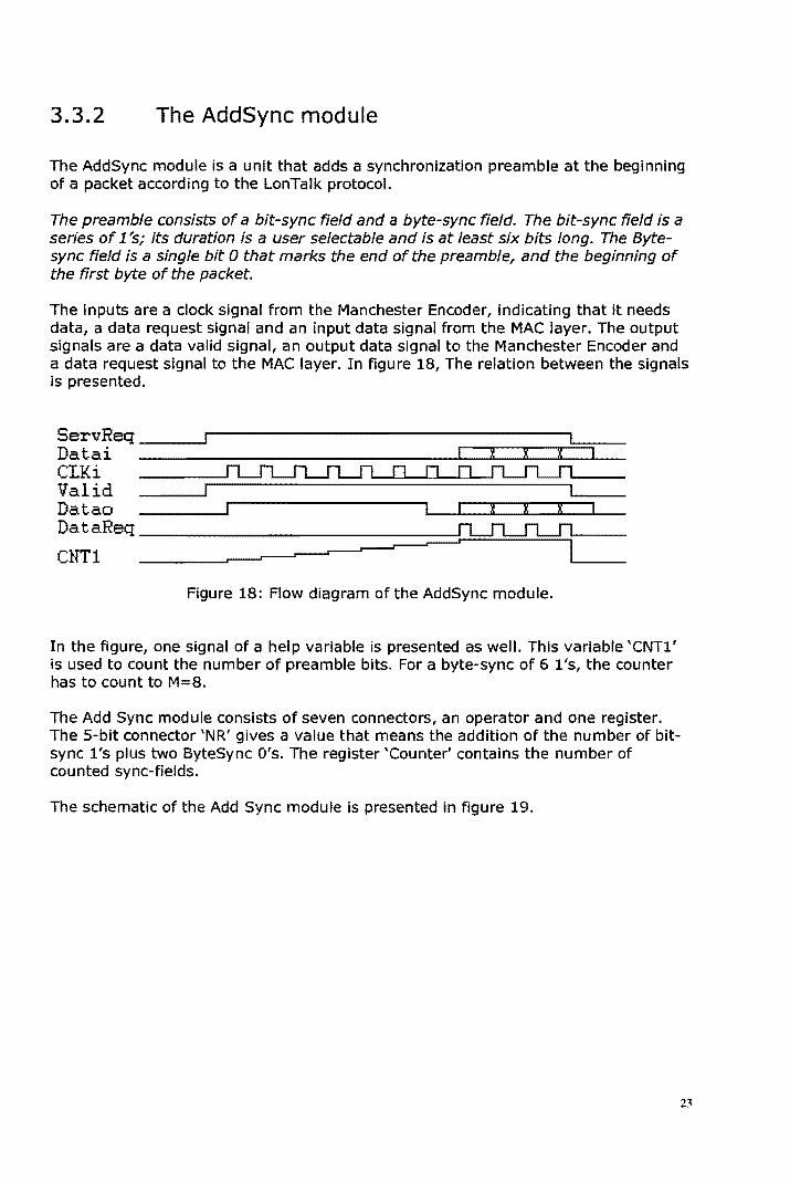
The inputs are a clock signal from the Manchester Encoder, indicating that it needs data, a data request signal and an input data signal from the MAC layer. The output signals are a data valid signal, an output data signal to the Manchester Encoder and a data request signal to the MAC layer. In figure 18, The relation between the signals is presented.
ServReq __ ----' Datai CIKi Valid Datao g g x
DataReq ______ ~==========:=~==~~~~~~~---CNT! __ ----'r--J I
Figure 18: Flow diagram of the AddSync module.
In the figure, one signal of a help variable is presented as well. This variable 'CNT1' is used to count the number of preamble bits. For a byte-sync of 61's, the counter has to count to M=8.
The Add Sync module consists of seven connectors, an operator and one register. The 5-bit connector 'NR' gives a value that means the addition of the number of bitsync l's plus two ByteSync Q's. The register 'Counter' contains the number of counted sync-fields.
The schematic of the Add Sync module is presented in figure 19.
23
Se~vReq .t------------;QL------~
I-----vll---~!II Va~:l d
D a.taRe q 1ISt------------"'1lL ____ ---1
I-----vll---~!II 1)a.t-ao AddS".nc
ClIiIT CN'To M
OF
Figure 19: The block schematic of the AddSync module.
24
3.4 The Collision Detector
As presented in figure 21, a transmitted bit stream is received with an unknown delay because of the magnetic coupling to the medium. The Collision detector is a unit that compares the outgoing data with the delayed incoming data. In case there is a difference between the data, it is assumable that a collision has taken place. For these errors and errors that are detected by an external unit, the unit chooses an appropriate error message. Dependent on the mode of operation, and the moment of detection, it sends an attention to the Port Controller.
There are three possible error indications; each assigned to another data bit of the error indication. If no error bit is true, it means that no error has occurred yet since the beginning of the transmission of the frame, or the last frame has been transmitted successfully.
I Request Denied I Collision Detected I Detection Error I
Request Denied is the error indication that happens if a collision has been detected (by this unit or an external device) before the transmission of the actual data started. More specific, before or during the synchronization period in Direct mode or before the first data bit in Special Purpose Mode. Collision Detected is set if this unit or the external device detects collision. More specific, if the incoming data stream does not equal the outgoing data stream. Detection Error is set in all cases an error occurs.
Possible cases that such error occurs are: • The collision detector is in the Sync_State or Wait_R_State, but the transmitting
unit is not sending (Valid line is false). • The receive FIFO is full due to a receiving higher layer that is too slow. • There is no activity on the line during the transmission. • More data is received than Transmitted. • Not all transmitted data is received.
In special Purpose Mode, transmission of an outgoing packet is aborted immediately upon detection of a collision or error. Then the MAC layer has to be notified that the collision occurred. The Collision Valid Register, which is reset by default, is used for this attention. In addition, the Collision Valid Register is activated at the end of the transmission of each frame to report the success of the transmission. In Direct Mode the MAC layer is attended only before (Collision Denied) and at the end of the transmission by the Collision Valid signal. The error bits indicate the success or errors of the transmission.
In Figure 20, the implementation of the Collision Detector is presented. The unit consists of the three transmission input connectors Valid, CLKi and Datao and three reception input Connectors: Idle, BitValid and Bitvalue. It also contains a setting input connector Mode, an external collision report input connector ColiDet and the two Output connectors Status and StatusValid which are connected to the registers Status and StatusValid. These registers and a FIFO are controlled by a state controller CNTRL.
25
The collision Detection unit contains a FIFO called OldData. The FIFO is filled with the incoming data bit at each ClKi signal pulse. At each BitValid pulse the first data bit is removed from the FIFO and compared with the BitValue at the input. If they differ, the collision Is detected.
Valid ~
OldData
Datao in ~OllDetl
CNTRL
Idle ~
III AI
III ItI S tatusVali em StatusValid
~
Figure20: Block diagram of the Collision Detector.
Because there are several kinds of operations and detections that have to be done sequentially, the unit is realized as a state machine. In figure 21, the flow of the incoming and outgoing data is shown, when a possible input signal is fed in Direct mode. It is possible to recognize six different states.
The upper arrows indicate the normal state transitions. The lower arrows indicate the escape transitions to the Output State in cases of an error. In these cases or if the external device detects a collision, the Status Register is actualized and the Status Valid Register is set.
26
The state controller is in the Idle_State after a system reset. In this state, the FIFO is emptied and the status register is set to 'success' (000) and the Status Valid Register is reset. The controller returns to this state every system clock cycle as long as the Valid input signal stays low. If this signal rises, the controller jumps to the next state. For the Direct mode, this is the Sync_State, for the Special Purpose Mode this is the Wait_R_State.
Valid ClKi Oatao
Idle
~ '7" '70 0.1 Idle_ ~ Sync_ ~ Wait_R_ 1" Compare_l_ :Comp_2_putput_:Idle_ State 1 State 1 State : State :State ~State :State __ ---!tr-~ _______ 1 ___ -;-_____ --i~ ~ ,.. .......... :
BitValid -----'>-----...:.------:f
Figure 21: Flow diagram of the Collision Detector.
In the Sync_State, the state controller waits for the 'ByteSync' bit and then jumps to the Wait Receive Data State. This happens when the 'OataO' line and the 'ClKi' pulse are low again. In this state, the error indication in the Status Register and the ColliSion Valid indication in the Status Valid Register can be activated if necessary.
In the Wait_R_State, each 'ClKi' pulse activates the FIFO to load the incoming data bits. If a 'BitValid' pulse is received, a jump to the Compare_i_State takes place after comparison of the received bit with the first bit in the FIFO, which is removed as well. Writing in a full FIFO means that the delay is too long and the error bit in the Status Register will be set.
In the Compare_l_State, each 'elKil pulse activates the FIFO to load the incoming data bits and each BitValid pulse removes the first bit out of the FIFO after comparison with the received data bit. If the frame is transmitted completely and therefore the Valid line falls, the state controller jumps to the Compare_2_State.
In the Compare_2_State, each BitValid pulse removes the first bit out of the FIFO after comparison with the received data bit. If the frame is received completely and therefore the Idle line rises, the state controller jumps to the Output_State.
In the Output_State, which is repeated every system clock cycle that the transmission or reception goes on (i.e. if valid or not idle), the Status Valid Register is set. If there is no activity anymore, the State controller jumps back to the Idle_State.
27
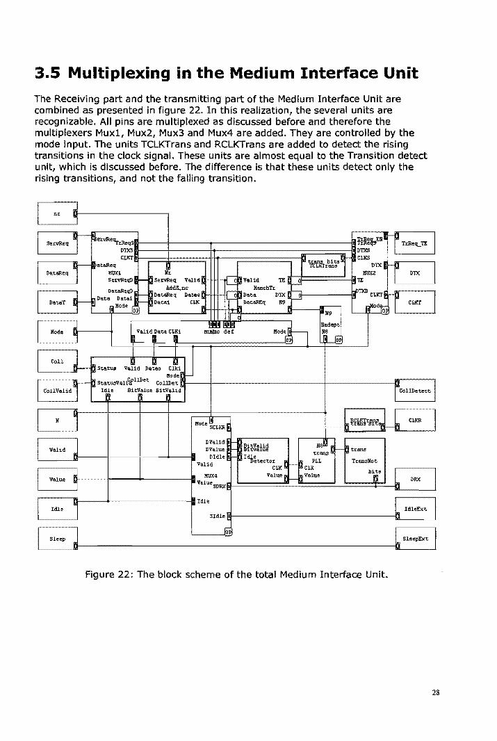
3.5 Multiplexing in the Medium Interface Unit
The Receiving part and the transmitting part of the Medium Interface Unit are combined as presented in figure 22. In this realization, the several units are recognizable. All pins are multiplexed as discussed before and therefore the multiplexers Muxl, Mux2, Mux3 and Mux4 are added. They are controlled by the mode input. The units TCLKTrans and RCLKTrans are added to detect the rising transitions in the clock signal. These units are almost equal to the Transition detect unit, which is discussed before. The difference is that these units detect only the rising transitions, and not the falling transition.
I n~ ~D----------'
I setvReq ,- ~ervRe~~~~II---__ -I ____ "'-____________ -I1Ir.J !~~ENa I TrRe~~ I I i -ataRe'! WIT I'" '¥i!firr~i' q-~ CL:~TX Ii DTX I
DataReq lI1lXl Nr I au .....
ServReql) 1-~ ServReq Valid C ro a Valid ~ ~ ,......-' ~ ~
I ~ Dat:a~:I~DJ 1_~D"t.:~s.,n;at"o~ UroI'":J~Dat:anChTrDTX K~ bPTXD CLXT~~ I D"taT ~ Hode -~ Datai eLK,. '" DataREq N9 ..-- ",ode- CLXT
I OP Ii - T ..... [J N9 101
I lIode J,n---__ .... Valid Data eLKi m:.J ~:~ /lode L ~~daPt ~~~==~==~=;==~============~~=p~JL l~~'~~o~_~
I eoll L a Status Valid Datao Clki lIode~ r-
I I ~ a Statu~Val11fllDet ColiDet n---I-----------f-.------.----l
CollValid I Id~e BitValue BitValid rCOllDetect
I ---M~HIL eLK!< I r- u- ... u __ ----' I N 1 /lode SCLKR~
I J DVal1~ ~ DValue Dldle
Valid
I Value J JruX4 , valueSDRXc
~ Bi tValid }IS ~, ~ ~ B1 tvalue f-- traru3 Idle trans
Detector P r- iN PLL TrensNot eLK ~ ~ CLK bits
Value E f-n Value n
I II Idle
Idle 1 SIdle t L IdleExt I
J I IOi
Sleep b SJ.eepExt
Figure 22: The block scheme of the total Medium Interface Unit.
28
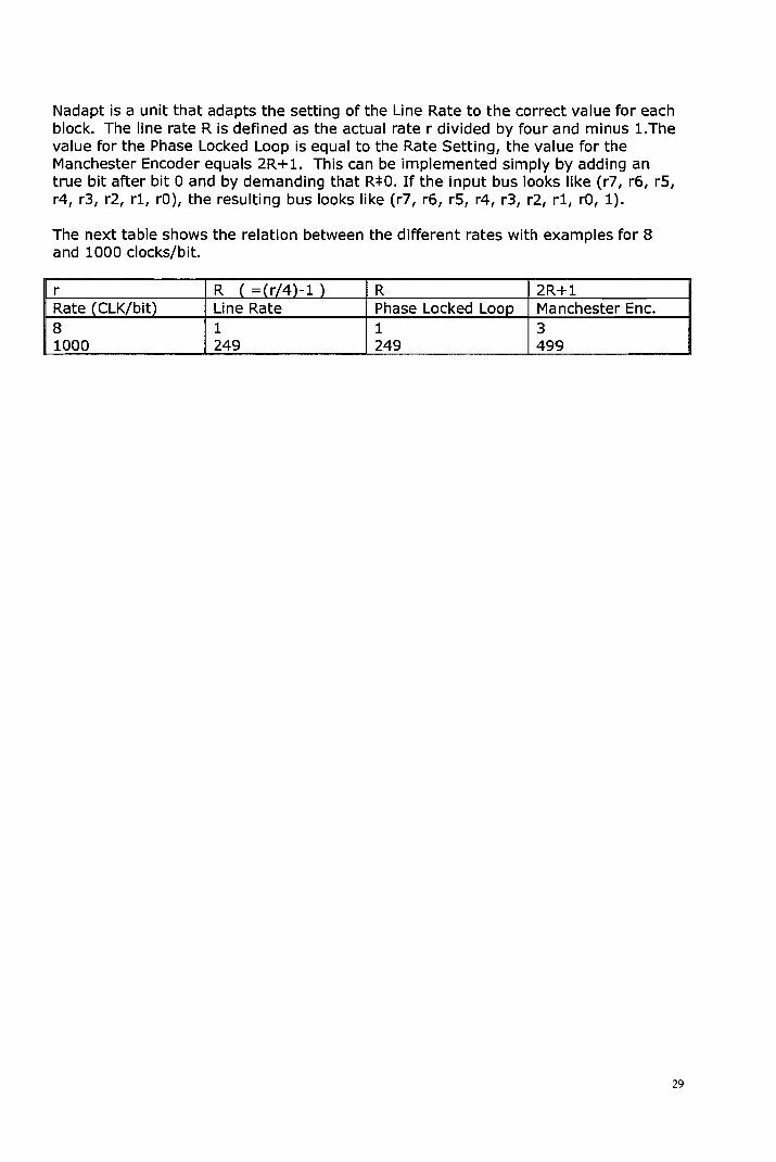
Nadapt is a unit that adapts the setting of the Line Rate to the correct value for each block. The line rate R is defined as the actual rate r divided by four and minus l.The value for the Phase locked loop is equal to the Rate Setting, the value for the Manchester Encoder equals 2R+1. This can be implemented simply by adding an true bit after bit 0 and by demanding that R*O. If the input bus looks like (r7, r6, rS, r4, r3, r2, rl, rO), the resulting bus looks like (r7, r6, rS, r4, r3, r2, rl, rO, 1).
The next table shows the relation between the different rates with examples for 8 and 1000 clocks/bit.
r R (=(r/4)-1) R 2R+l Rate (elK/bit) Line Rate Phase Locked Loop Manchester Enc. 8 1 1 3 1000 249 249 499
29
4 The Codec and Convert unit 4.1 Introduction The Codec and Convert unit handles all operations at Byte level, including the transformation from bytes to bits and visa versa. In the LonTalk Protocol, the only function of the byte controller is a fault detection codec.
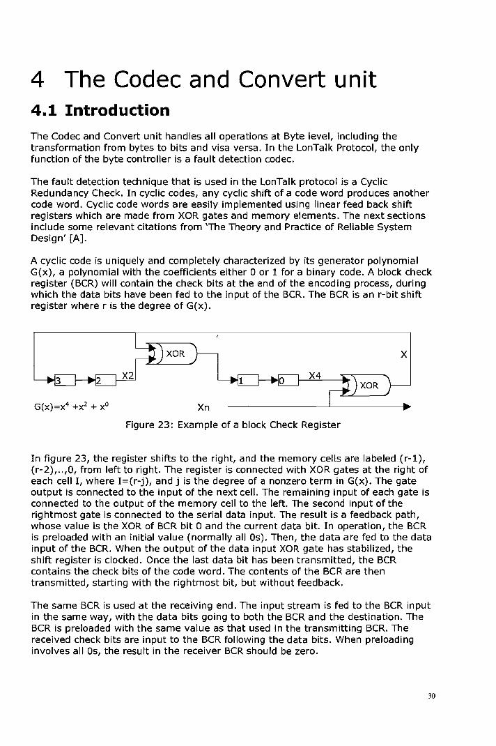
The fault detection technique that is used in the LonTalk protocol is a Cyclic Redundancy Check. In cyclic codes, any cyclic shift of a code word produces another code word. Cyclic code words are easily implemented using linear feed back shift registers which are made from XOR gates and memory elements. The next sections include some relevant citations from 'The Theory and Practice of Reliable System Design' [AJ.
A cyclic code is uniquely and completely characterized by its generator polynomial G(x), a polynomial with the coefficients either ° or 1 for a binary code. A block check register (BCR) will contain the check bits at the end of the encoding process, during which the data bits have been fed to the input of the BCR. The BCR is an r-bit shift register where r is the degree of G(x).
x
Xn
Figure 23: Example of a block Check Register
In figure 23, the register shifts to the right, and the memory cells are labeled (r-l), (r-2), .. ,0, from left to right. The register is connected with XOR gates at the right of each cell I, where I=(r-j), and j is the degree of a nonzero term in G(x). The gate output is connected to the input of the next cell. The remaining input of each gate is connected to the output of the memory cell to the left. The second input of the rightmost gate is connected to the serial data input. The result is a feedback path, whose value is the XOR of BCR bit 0 and the current data bit. In operation, the BCR is preloaded with an initial value (normally all Os). Then, the data are fed to the data input of the BCR. When the output of the data input XOR gate has stabilized, the shift register is clocked. Once the last data bit has been transmitted, the BCR contains the check bits of the code word. The contents of the BCR are then transmitted, starting with the rightmost bit, but without feedback.
The same BCR is used at the receiving end. The input stream is fed to the BCR input in the same way, with the data bits going to both the BCR and the destination. The BCR is preloaded with the same value as that used in the transmitting BCR. The received check bits are input to the BCR following the data bits. When preloading involves aliOs, the result in the receiver BCR should be zero.
30
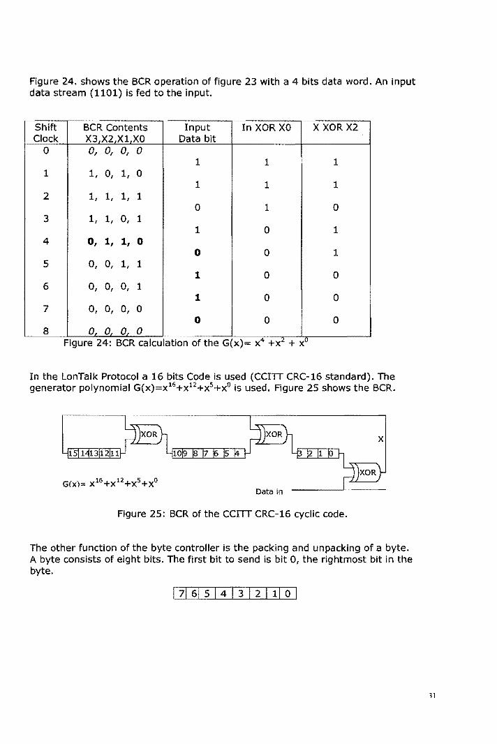
Figure 24. shows the BCR operation of figure 23 with a 4 bits data word. An input data stream (1101) is fed to the input.
Shift BCR Contents Input In XOR XO X XOR X2 Clock X3 /X2 /Xl XO Data bit
0 0, 0, 0, 0 1 1 1
1 11 0, 11 0 1 1 1
2 11 11 11 1 0 1 0
3 11 11 0, 1 1 0 1
4 0, 1, 1, 0 0 0 1
5 01 01 11 1 1 0 0
6 01 01 01 1 1 0 0
7 01 0, 01 0 0 0 0
8 0, 0, 0, 0 Figure 24: BCR calculation of the G(x)= X4 +X2 + XO
In the LonTalk Protocol a 16 bits Code is used (CCITT CRC-16 standard). The generator polynomial G(X)=X16+X12+XS+XO is used. Figure 25 shows the BCR.
Figure 25: BCR of the CCITT CRC-16 cyclic code.
The other function of the byte controller is the packing and unpacking of a byte. A byte consists of eight bits. The first bit to send is bit 0, the rightmost bit in the byte.
LZL§I 5 I 4 I 3 I 2 111 0 I
31
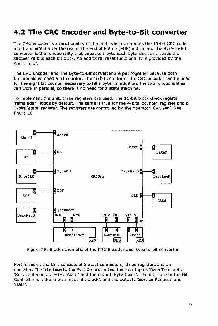
4.2 The CRe Encoder and Byte-to-Bit converter
The CRC encoder is a functionality of the unit, which computes the 16-bit CRC code and transmits it after the rise of the End of Frame (EOF) indication. The Byte-to-Bit converter is the functionality that unpacks a byte each byte clock and sends the successive bits each bit clock. An additional reset functionality is provided by the Abort input.
The CRC Encoder and The Byte-to-Bit converter are put together because both functionalities need a bit counter. The 16 bit counter of the CRC encoder can be used for the eight bit counter necessary to fill a byte. In addition, the two functionalities can work in parallel, so there is no need for a state machine.
To implement the unit, three registers are used. The 16-bit block check register 'remainder' loads by default. The same is true for the 4-bits 'counter' register and a 3-bits 'state' register. The registers are controlled by the operator 'CRCGen'. See figure 26.
111
j!I Al:l o:t:t Ilj
A.bor::d
DateD :
~Dt ~
~ DateD Dt
I!J =a. teCLK Ser::vReqD: ~
a. teCLK CRCGen 5ervReqD
i!J EOF aI eLK ~ ~ EOF
CLKd
ij ServRequ Kl ClITo ClIT STo ST 5ervReqU Re:m.O Rem
II] n 111 II [11 lilop
n IIJ II IJ I [II Remainder Counter:: State
rm ffiE'G jM
Figure 26: Block schematic of the CRC Encoder and Byte-to-bit converter
Furthermore, the Unit consists of 8 input connectors, three registers and an operator. The interface to the Port Controller has the four inputs 'Data Transmit', 'Service Request', 'EOF', 'Abort' and the output 'Byte Clock'. The interface to the Bit Controller has the known input 'Bit Clock', and the outputs 'Service Request' and 'Data'.
32
There are 4 states: • state 0 is the begin state 'Ready to transmit', • state 1 is the state after the 'Request to transmit', • state 2 is the 'Data transmit' state, • state 3 is the 'CRC transmit' state, • state 4 is the state during the 'Last CRC bit'.
In state 2, the bits are fed to the BCR. In state 3, the bits of the resulting CRC code are output sequentially. The BCR is initially loaded with zero. Then the input bits are XOR-ed with the 'remainder' as explained, and stored again.
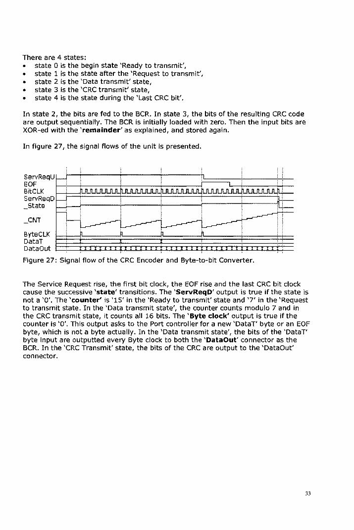
In figure 27, the signal flows of the unit is presented.
SerVReqUt=t __ l-______ -1 ________ 1-______ ~~====~Jt======j·J·t== EOF BitCLK ServReqD _State LJ--f-----+----~----r----;---1
_CNT
ByteCLK DataT DataOut
Figure 27: Signal flow of the CRC Encoder and Byte-to-bit Converter.
The Service Request rise, the first bit clock, the EOF rise and the last CRC bit clock cause the successive 'state' transitions. The 'ServReqD' output is true if the state is not a '0'. The 'counter' is '15' in the 'Ready to transmit' state and '7' in the 'Request to transmit state. In the 'Data transmit state', the counter counts modulo 7 and in the CRC transmit state, it counts all 16 bits. The 'Byte clock' output is true if the counter is '0'. This output asks to the Port controller for a new 'DataT' byte or an EOF byte, which is not a byte actually. In the 'Data transmit state', the bits of the 'DataT' byte input are outputted every Byte clock to both the 'DataOut' connector as the BCR. In the 'CRC Transmit' state, the bits of the CRC are output to the 'DataOut' connector.
33
4.3 The CRC Decoder and the Bit-to-Byte converter
The CRC Decoder of the unit computes the i6-bit CRC code over the received bits, and indicates every time a byte is received, whether the BCR equals zero or not. If the frame and the added CRC code are transmitted correct, the unit will indicate a zero. Furthermore, it is possible that a zero is indicated in the middle of the frame. It's the job for the upper layer to reason that the frame length is not reached yet and so the indication is not correct.
The Bit-to-Byte converter has the functionality to pack 8 received bits in a byte, and to give it through to the port controller. This gives an 8-bit time delay. In addition, each bit has to be accompanied by the CRC indication bit, which takes a 16 bits time delay. Therefore, the first byte will be transmitted 24 bit clocks later than the reception of the first bit.
The CRC indication bit and the Bit-to-Byte result byte are grouped in the following way.
I Bit 7 I Bit 6 I Bit 5 I. Bit 4. I Bit 3 I Bit 2 1m Bit 1 I Bit 0 I CRC
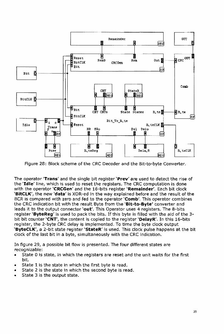
To implement the unit, four operators, 6 registers and 5 connectors are used as presented in figure 28.
34
Remainder: OUT II m I
,-I Reset I]
1:1 CRC OUT I - RemO Rem Oue II BieCLK CRCGen III !::I
I Bie
Bit U\ ~
Comb cn [Stjt~
BitCLK: 11 JIJw
~Bit cUr c~o II !I State Stateo a. ee II l!Ia. te
- BBitCLK 'II
lOP Klr--i!li 0 Ii-'"
~Reset Bi t_To_a. te
a. teCLK: Idle '----ll:8IlS BR BRo Del Delo ~I1t1fQp n ~ m II fii'F
g t It I i I Pt:ev a. teReg Dela,.R a. teCLK
!REG ~ !REG
Figure 28: Block scheme of the CRC Decoder and the Bit-to-byte Converter.
The operator 'Trans' and the single bit register 'Prey' are used to detect the rise of the 'Idle' line, which is used to reset the registers. The CRC computation is done with the operator 'CRCGen' and the 16-bits register 'Remainder'. Each bit clock 'BitCLK', the new 'data' is XOR-ed in the way explained before and the result of the BCR is compared with zero and fed to the operator 'Comb'. This operator combines the CRe indication bit with the result Byte from the 'Bit-to-Byte' converter and leads it to the output connector 'out'. This Operator uses 4 registers. The 8-bits register 'ByteReg' is used to pack the bits. If this byte is filled with the aid of the 3-bit bit counter 'CNT', the content is copied to the register 'OelayR'. In this 16-bits register, the 2-byte CRC delay is implemented. To time the byte clock output 'ByteCLK', a 2-bit state register 'StateR' is used. This clock pulse happens at the bit clock of the last bit in a byte, simultaneously with the CRC indication.
In figure 29, a possible bit flow is presented. The four different states are recognizable: • State 0 is state, in which the registers are reset and the unit waits for the first
bit. • State 1 is the state in which the first byte is read. • State 2 is the state in which the second byte is read. • State 3 is the output state.
35
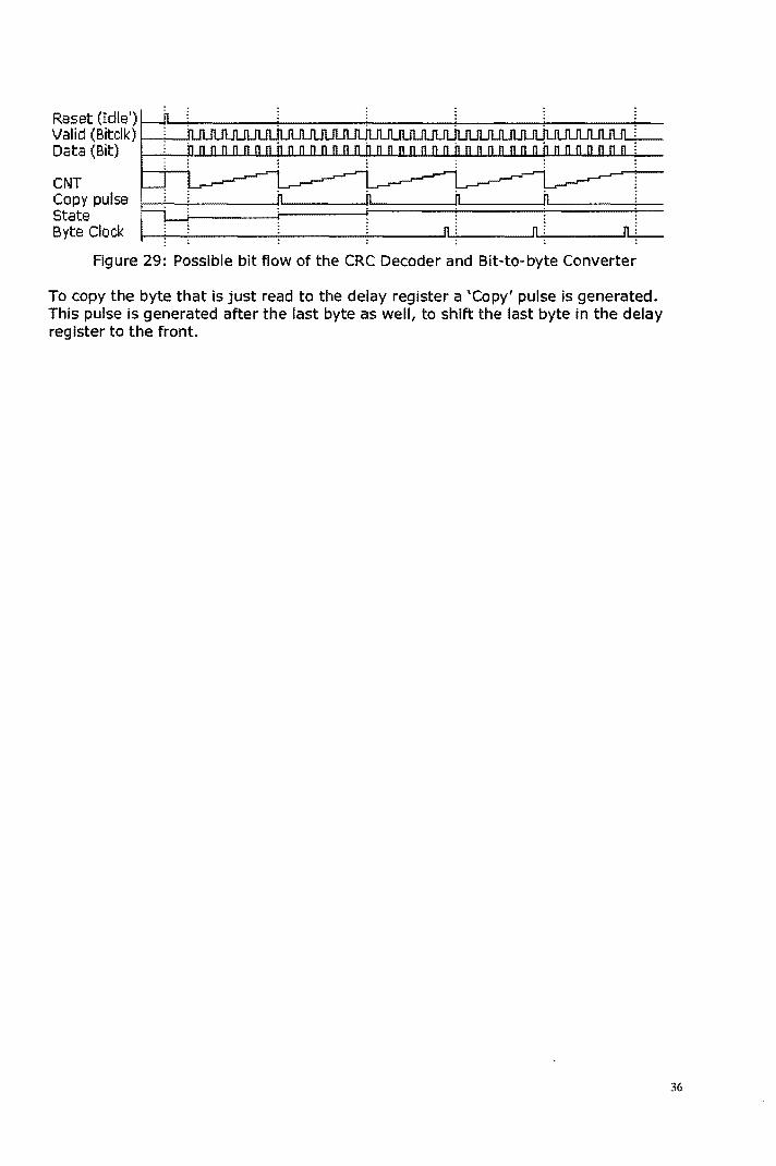
Reset (Idle') f--~L..-+----~----+-----i-----i--------fValid (Bitclk) I----;,.-...-.J
Data (Bit)
CNT Copy pulse State Byte Clock
Figure 29: Possible bit flow of the CRC Decoder and Bit-to-byte Converter
To copy the byte that is just read to the delay register a 'Copy' pulse is generated. This pulse is generated after the last byte as well, to shift the last byte in the delay register to the front.
36
5 The Processor Interface Unit
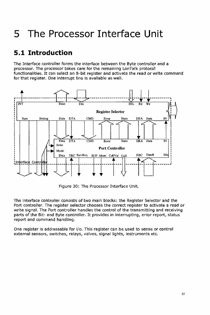
5.1 Introduction The Interface controller forms the interface between the Byte controller and a processor. The processor takes care for the remaining LonTalk protocol functionalities. It can select an a-bit register and activate the read or write command for that register. One interrupt line is available as well.
r-- ----------------- -------------------- --- --- ----------, ! ~m~T------------~~--L---~~------------------~~~~~-------, ! I I I I I I
Register Selector
I Rate Setting Data DT A CMD I I I I I I I I I I I I
I I I I I I I I I I I I I I I I I I I I
LI!! ~'!~S _£~ g- 1
r-~~~~----~=---~E~IT-orL-~~S~ta-tu~--~~~-L--~m~ :
Port Controller I I I I I I
Lr~~~~,---~=EOrF~Arbo=rt~C=o7I1V~a~I~CTo~J1~--~--~~----~ :
Figure 30: The Processor Interface Unit.
I I ___________ .J
The interface controller consists of two main blocks: the Register Selector and the Port controller. The register selector chooses the correct register to activate a read or write signal. The Port controller handles the control of the transmitting and receiving parts of the Bit- and Byte controller. It provides in interrupting, error report, status report and command handling.
One register is addressable for i/o. This register can be used to sense or control external sensors, switches, relays, valves, signal lights, instruments etc.
37
5.2 The Register Selector
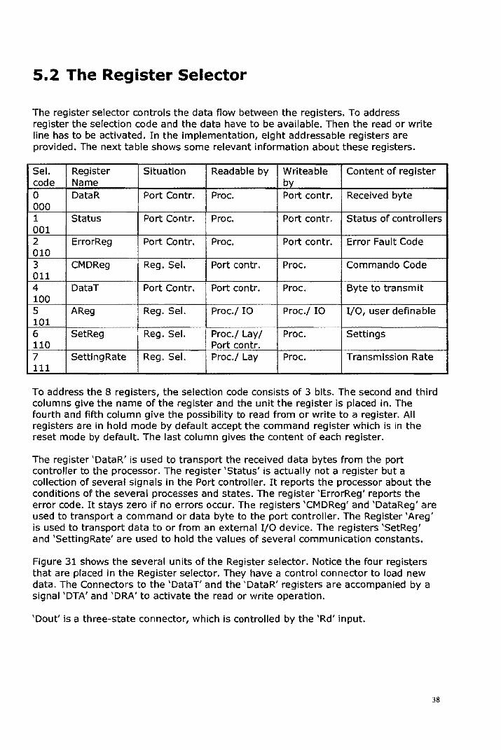
The register selector controls the data flow between the registers. To address register the selection code and the data have to be available. Then the read or write line has to be activated. In the implementation, eight addressable registers are provided. The next table shows some relevant information about these registers.
Sel. Register Situation Readable by Writeable Content of register code Name by 0 DataR Port Contr. Proc. Port contr. Received byte 000 1 Status Port Contr. Proc. Port contr. Status of controllers 001 2 ErrorReg Port Contr. Proc. Port contr. Error Fault Code 010 3 CMDReg Reg. Sel. Port contr. Proc. Commando Code 011 4 DataT Port Contr. Port contr. Proc. Byte to transm it 100 5 AReg Reg. Sel. Proc./ 10 Proc.j 10 I/O, user definable 101 6 SetReg Reg. Sel. Proc./ Lay/ Proc. Settings 110 Port contr. 7 Setting Rate Reg. Sel. Proc./ Lay Proc. Transmission Rate 111
To address the 8 registers, the selection code consists of 3 bits. The second and third columns give the name of the register and the unit the register is placed in. The fourth and fifth column give the possibility to read from or write to a register. All registers are in hold mode by default accept the command register which is in the reset mode by default. The last column gives the content of each register.
The register 'DataR' is used to transport the received data bytes from the port controller to the processor. The register 'Status' is actually not a register but a collection of several signals in the Port controller. It reports the processor about the conditions of the several processes and states. The register 'ErrorReg' reports the error code. It stays zero if no errors occur. The registers 'CMDReg' and 'DataReg' are used to transport a command or data byte to the port controller. The Register 'Areg' is used to transport data to or from an external I/O device. The registers 'SetReg' and 'SettingRate' are used to hold the values of several communication constants.
Figure 31 shows the several units of the Register selector. Notice the four registers that are placed in the Register selector. They have a control connector to load new data. The Connectors to the 'DataT' and the 'DataR' registers are accompanied by a signal 'DTA' and 'DRA' to activate the read or write operation.
'Dout' is a three-state connector, which is controlled by the 'Rd' input.
38
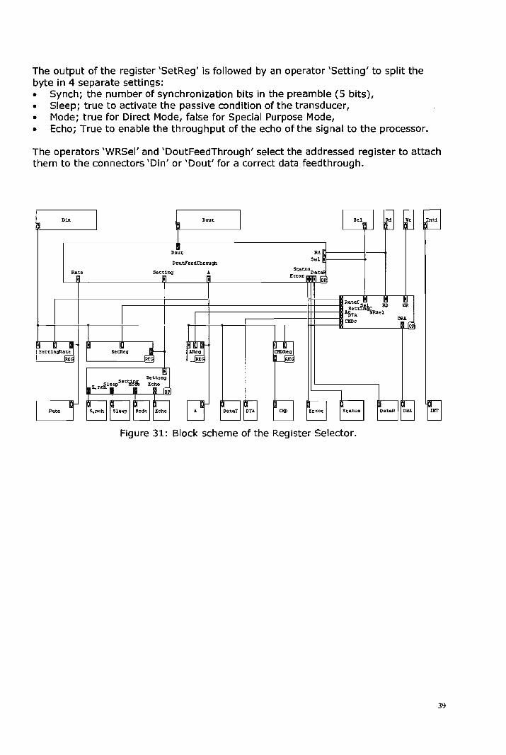
The output of the register 'SetReg' is followed by an operator 'Setting' to split the byte in 4 separate settings: • Synch~ the number of synchronization bits in the preamble (5 bits), • Sleep~ true to activate the passive condition of the transducer, • Mode~ true for Direct Mode, false for Special Purpose Mode, • Echo; True to enable the throughput of the echo of the signal to the processor.
The operators 'WRSel' and 'DoutFeedThrough' select the addressed register to attach them to the connectors 'Din' or 'Dout' for a correct data feedthrough.
Eu:ot Itrr
Figure 31: Block scheme of the Register Selector.
39
5.3 The Port Controller
The Port controller is the unit that handles the control of the transmitting and receiving parts of the Bit- and Byte controller. It provides timing, interrupting, error reporting, status reporting and command handling. It forms the interface between the sequential and parallel parts of the system. The processor can handle only one byte at a time. The transmitting and the receiving parts operate in parallel. To let the se three units operate at the same time, two FIFO memories are used: One for the bytes to transmit and one for the received bytes. A block scheme is presented in figure 32.
5.3.1 The transmit side
The transmit side consists of an operator, two FIFO registers and an output register. These three 10-bit registers contain the data Byte at bit places 2 to 9. Data to transmit is shifted in the last free register via the 'Dt' input by activating the 'DTA' line. Each time the transmit byte clock is high, all data shifts to the next register. The data in the first register is shifted to the output register. At bit place 1, the bit indicates the availability of the data. The data bit in the register is set to 'available' if the register is written with new data; i.e. new data is shifted in the register. The bit is reset if the data is shifted out of the register and no new data is shifted in the register. At bit place 0, the bit indicates that the register does not contain data but that it indicates the end of the Frame (EOF). An EOF byte is inserted by a command from the command operator, in stead of the 'DTA' signal. When shifting the EOF byte in the output register, by the rise of the transmit byte clock, the 'EOFOut' line rises and the eRe encoder will start sending the BeR. An abort command from the command operator is sent to the eRe-encoder directly. In addition, it resets all the registers.
To control the ServReq line an additional single bit register is used. This register called 'sending' is set if the available bit in the output register is set. The 'Sending' register is reset if the EOF byte is shifted in the output register. The ServReq indication gives the value of the Sending register. Note that the ServReq line indicates the request to transmit the data bytes. During the transmission of the eRe code, the line will not be high.
Furthermore, the transmitting side reports its condition via an interrupt line, an error line and two lines indicating the availability of data in the first and in the last register of the FIFO.
Notice that the 'DataT' register, mentioned in paragraph 5.2, is not a specific register, but the last data place in the 'Tfifo'.
40
5.3.2 The receive side
The receive side consists of an operator, two FIFO registers and an output register as we". These three lO-bit registers contain the data Byte at bit places 2 to 9. Received data is shifted in the last free register via the 'ORin' input by activating the 'ReceiveByte clock'. Each time the 'ORA' line is high, all data shifts to the next register. The data in the first register is shifted to the output register. At bit place 1, the bit indicates the availability of the data. The data bit in the register is set to 'available' if the register is written with new data; i.e. new data is shifted in the register. The bit is reset if the data is shifted out of the register and no new data is shifted in the register. At bit place 0, the CRC bit is placed. A false value indicates that the frame was transmitted correct if the byte was the last one of the frame. An abort command from the command operator resets a" the registers. A special service is the ability to choose whether the received data, which is an echo of the transmitted ones, will be or will not be sent back to the processor for a possible special processing. In normal cases, this option will not be chosen. This means that an activation of the receive byte clock must not result in filling the FIFO. A single bit register 'EchoLock' is set if a transmission starts and reset when the channel is idle. By using this register, the operator can decide on reception whether it is an echo or not and whether the data has to be passed or not.
Furthermore, the receiving side reports its condition via an interrupt line, an error line and two lines indicating the availability of data in the first and in the last register of the FIFO.
41
5.3.3 Error handling and control
For the error handling and control of the LonTalk protocol interface, a command unit, an error register, a status register and an interrupt unit are provided. These units take care for a kind of handshake with the processor. The common idea is that all actions on special events, like an error, idle state of channel or the reception of a new data byte, are taken by the processor.
An interrupt is given to alert the processor that a special event has occurred. It is the processor's job to find out what event caused the interrupt and to act on it. This will be done by reading the status register first. In the status register, each bit represents a special condition, which is useful to control the interface. This can be the state of the channel, but also the cause of an interrupt. With this information, the processor knows what to do. The interrupt line will stay high until the problem is solved. In some cases, like the reception of a byte, the interrupt line falls immediately on reading the output register. In other cases, as if the end of a frame or an error, the processor has to reset a bit in a register (Error register or Frame Result register) This shows that the event is attended. Resetting a bit in the Error register or Frame Result register can only be done by giving a command to the Command unit, which will then reset the bit.
In this LonTalk port controller, four special events can cause an interrupt:
• The first one is the Transmit Interrupt. This interrupt is given when the unit is sending and its FIFO is not completely filled, provided that the EOF byte is not present in the Transmit FIFO. In this way, the FIFO will mostly be filled and so the byte controller will never have a lack of data during the transmission of a frame. The related status bit resets immediately on a filled FIFO.
• The second one is the Receive Interrupt. This interrupt is given if received data is available in the output register. If the processor is quick enough, the FIFO will not overflow in this way. The related status bit resets immediately on an empty FIFO.
• The third one is the Frame Result interrupt. This interrupt is given when a frame is received completely or if a collision or collision error happened (i.e. if the collision valid line rose). On this interrupt, the processor has to give a reset command for the related bit in the status register.
• The last one is the Error interrupt. This interrupt is given if an error takes place. An exception forms the case when the unit is sending in Special Purpose Mode and a collision or a collision error happens. Interrupting in this case has no sense, because the reception has to be competed according to the protocol specifications. However, the related Error register and the Status register (i.e. the Frame register in this case) will be set. On this interrupt, the processor has to give a reset command for the related bit in the status register.
42
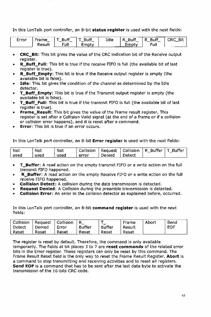
In this LonTalk port controller, an a-bit status register is used with the next fields:
Idle R_BufC CRC_Bit Full
• CRC_Bit: This bit gives the value of the CRC indication bit of the Receive output register.
• R_Buff_Full: This bit is true if the receive FIFO is full (the available bit of last register is true).
• R_Buff_Empty: This bit is true if the Receive output register is empty (the available bit is false).
• Idle: This bit gives the condition of the channel as determined by the Idle detector.
• T_Buff_Empty: This bit is true if the Transmit output register is empty (the available bit is false).
• T_Buff_Full: This bit is true if the transmit FIFO is full (the available bit of last register is true).
• Frame_Result: This bit gives the value of the Frame result register. This register is set after a Collision Valid signal (at the end of a frame or if a collision or collision error happens), and it is reset after a command.
• Error: This bit is true if an error occurs.
In this LonTalk port controller, an a-bit Error register is used with the next fields:
Not used
Not used
Not used
Collision Request Collision R_Buffer T _Buffer error Denied Detect
• T_Buffer: A read action on the empty transmit FIFO or a write action on the full transmit FIFO happened.
• R_Buffer: A read action on the empty Receive FIFO or a write action on the full receive FIFO happened.
• Collision Detect: A collision during the data transmission is detected. • Request Denied: A Collision during the preamble transmission is detected. • Collision Error: An error in the collision detector as explained before, occurred.
In this LonTalk port controller, an a-bit command register is used with the next fields:
Collision Request Collision R_ T_ Frame Abort Send Detect Denied Error Buffer Buffer Result EOF Reset Reset Reset Reset Reset Reset
The register is reset by default. Therefore, the command is only available temporarily. The fields at bit places 3 to 7 are reset commands of the related error bits in the Error register. These registers can only be reset by this command. The Frame Result Reset field is the only way to reset the Frame Result Register. Abort is a command to stop transmitting and receiving activities and to reset all registers. Send EOF is a command that has to be sent after the last data byte to activate the transmission of the 16-bits CRC code.
43
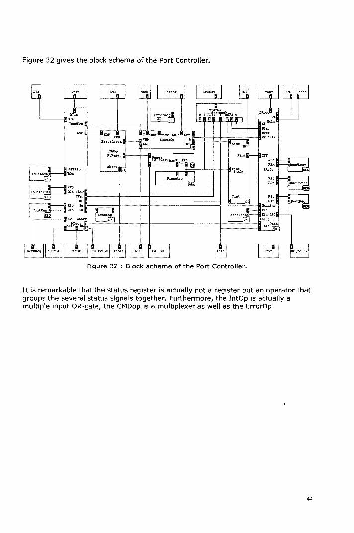
Figure 32 gives the block schema of the Port Controller.
Figure 32 : Block schema of the Port Controller.
It is remarkable that the status register is actually not a register but an operator that groups the several status signals together. Furthermore, the IntOp is actually a multiple input OR-gate, the CMDop is a multiplexer as well as the ErrorOp.
44
6 Testing 6.1 Introduction
This chapter describes the way the units and combination of units are tested. Testing is done by feeding the units a data flow and checking the outputs. If the outputs had a correct response to the input, the same was done with combination of units until the total design responded in the correct way.
In the beginning, when data flows had to be fed a unit is made in which the wished data flow can be stored and that produces a bit every system clock. Later, when total bytes had to be tested, an eight bits temporarily register could do the job. The response can be checked by connecting an IDaSS Viewer on the outputs or registers.
In the previous chapters the data flows of the inputs and outputs and important registers were presented of the separated units. The units responded in the desired way as described before. In this chapter, the combinations of the several units are described.
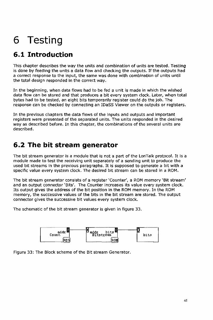
6.2 The bit stream generator
The bit stream generator is a module that is not a part of the LonTalk protocol. It is a module made to test the receiving unit separately of a sending unit to produce the used bit streams in the previous paragraphs. It is supposed to generate a bit with a specific value every system clock. The desired bit stream can be stored in a ROM.
The bit stream generator consists of a register 'Counter', a ROM memory 'Bit stream' and an output connector 'Bits'. The Counter increases its value every system clock. Its output gives the address of the bit position in the ROM memory. In the ROM memory, the successive values of the bits in the bit stream are stored. The output connector gives the successive bit values every system clock.
The schematic of the bit stream generator is given in figure 33.
bits
Figure 33: The Block scheme of the Bit stream Generator.
45
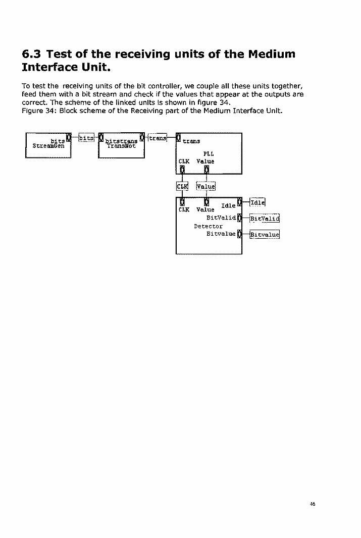
6.3 Test of the receiving units of the Medium Interface Unit.
To test the receiving units of the bit controller, we couple all these units together, feed them with a bit stream and check if the values that appear at the outputs are correct. The scheme of the linked units is shown in figure 34. Figure 34: Block scheme of the Receiving part of the Medium Interface Unit.
bits Stream.Gen
PLL
Detector
46
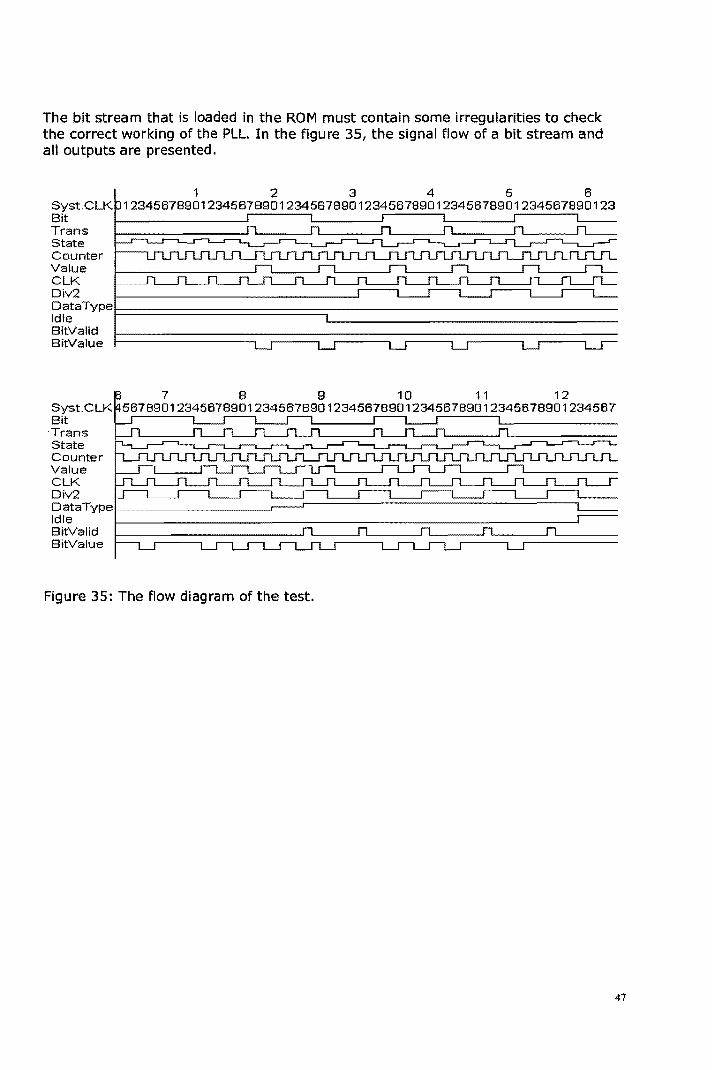
The bit stream that is loaded in the ROM must contain some irregularities to check the correct working of the PLL. In the figure 35, the signal flow of a bit stream and all outputs are presented.
1 2 3 4 5 6 Syst.CLK 123458789012345678901234567890123456789012345878901234567890123 Bit Trans State Counter Value CLK Div2
DataTypec=======================~=================================== Idle I BitValid BitValue
7 8 9 10 11 12 Syst.CLK 587890123456789012345678901234567890 1234567890 12345678901234567 Bit
'Trans State Counter Value CLK
Div2 ~ ___ ~~ __ ~==~ __ ~==~~==~ __ -===~ __ ~==~ __ ~==~~~~ DataType, Idle BitValid BitValue
Figure 35: The flow diagram of the test.
47
6.4 Test of the sending part and the receiving part of Medium Interface Unit
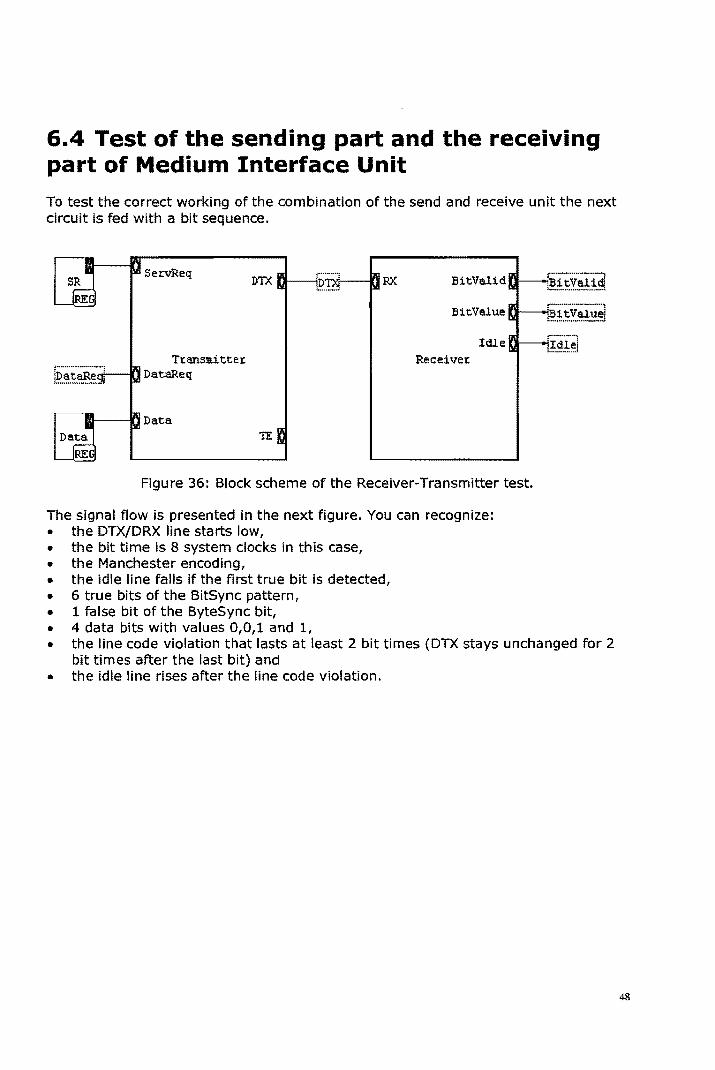
To test the correct working of the combination of the send and receive unit the next circuit is fed with a bit sequence.
SeI:vReq
Tt:ansm.ittet: -'----"I DataReq
GJ---nData
, DTX [I-----i~.~ JU RX ~ BitValid:
BitValue~
Idle~ Receivet:
Figure 36: Block scheme of the Receiver-Transmitter test.
The signal flow is presented in the next figure. You can recognize: • the DTX/DRX line starts low, • the bit time is 8 system clocks in this case, • the Manchester encoding, • the idle line falls if the first true bit is detected, • 6 true bits of the BitSync pattern, • 1 false bit of the ByteSync bit, • 4 data bits with values 0,0,1 and 1,
i ~:~!i.y..~!I~
Bi·tv~i";;~ : ..... _ ............ _.:
idi;l --j ................ !
• the line code violation that lasts at least 2 bit times (DTX stays unchanged for 2 bit times after the last bit) and
• the idle line rises after the line code violation.
48
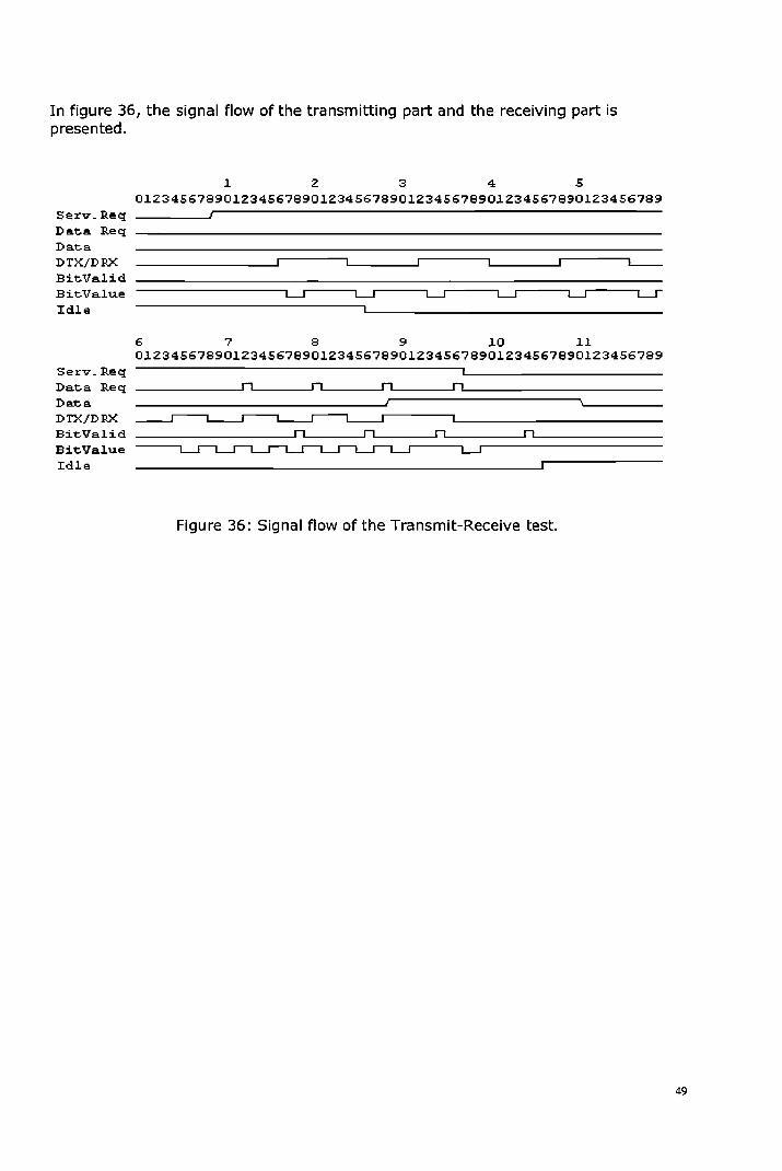
In figure 36, the signal flow of the transmitting part and the receiving part is presented.
Serv.Req Data Req Data DTX/DPX BitValid BitValue Idle
Servo Req Data Req Data DTX/DPX BieValid BitValue Idle
1 2 3 4 5 012345678901234567890123456789012345678901234567890123456789 ,
-----------------,~r----,~r----'~r----'~.----.~r----,L-r
6 7 8 9 10 11 012345678901234567890123456789012345678901234567890123456789
____________ ~nL ____ ~nL ____ ~nL ____ ~nL ______________________ _ I
n
Figure 36: Signal flow of the Transmit-Receive test.
49
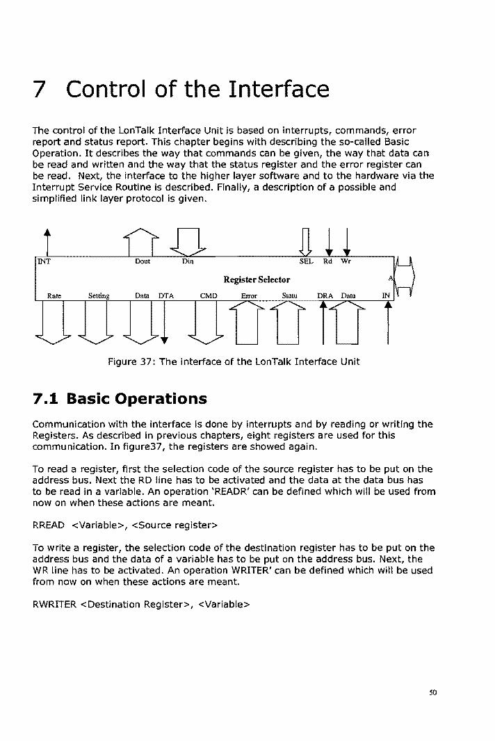
7 Control of the Interface
The control of the LonTalk Interface Unit is based on interrupts, commands, error report and status report. This chapter begins with describing the so-called Basic Operation. It describes the way that commands can be given, the way that data can be read and written and the way that the status register and the error register can be read. Next, the interface to the higher layer software and to the hardware via the Interrupt Service Routine is described. Finally, a description of a possible and simplified link layer protocol is given.
INT
Register Selector
Data DTA CMD
Figure 37: The interface of the LonTalk Interface Unit
7.1 Basic Operations
Communication with the interface is done by interrupts and by reading or writing the Registers. As described in previous chapters, eight registers are used for this communication. In figure37, the registers are showed again.
To read a register, first the selection code of the source register has to be put on the address bus. Next the RD line has to be activated and the data at the data bus has to be read in a variable. An operation 'READR' can be defined which will be used from now on when these actions are meant.
RREAD <Variable>, <Source register>
To write a register, the selection code of the destination register has to be put on the address bus and the data of a variable has to be put on the address bus. Next, the WR line has to be activated. An operation WRITER' can be defined which will be used from now on when these actions are meant.
RWRITER < Destination Register>, <Variable>
50
7.2 A Link layer Protocol interface
The software that runs the sending and receiving of packets is described in the link Protocol. This software forms the link between the higher layer software and the implemented LonTalk Interface hardware. This section and the next sections are meant to describe the usage of the hardware and do not contain the complete description of the LonTalk Protocol: The CSMA description and some facilities for it are left out.
Interrupt Service Routine Hardware events that are important for the program flow of the link protocol are reported to this software with interrupts. These interrupts cause the processor to jump to an Interrupt Service Routine (ISR) after storing the relevant actual data. After completing the ISR, the processor continues its previous activities with the stored data. In the ISR, variables can be changed to influence the link protocol program flow.
On a Hardware interrupt, the status register is read first. With this byte, it is possible to detect which kind of interrupt is meant. There are four possibilities: • Receive Interrupt. The R_BufCEmpty bit in the status register is False. This
interrupt results in setting the Rec_Data_Av flag during the ISR. In addition, the Data register is read and the byte is stored in the temporary variable ActuaLR_Data.
• Frame Result interrupt. The FR_Result bit in the status register is True. This interrupt results in setting the FR_Res_Av flag during the ISR. In addition, the Error register is read to determine the frame status. This status is stored in the variable ActuaLFR
• Error interrupt. The error bit in the status register is True. This interrupt results in setting the Error_Av flag during the ISR. In addition, the Error register is read to determine the kind of error. This error is stored in the variable ActuaLError
• Transmit Interrupt. The T_BufCFull bit in the status register is False. This interrupt results only in setting the Waiting_for_Transmission flag during the ISR.
After the treatment of the cause of the interrupt, the concerning flag is reset.
Communication with the higher layer software. Higher layer software that produces events that are important for the program flow of the link protocol reports these events by setting a flag, i.e. a shared variable. In the other way, if the Link Protocol software produces an event that is important for the higher layer software, the Link protocol software sets a flag. In both cases, the flag is reset after the treatment of the cause of this software interrupt. Besides interrupts, a transmit buffer and a receive buffer are used for the communication.
There are six software interrupts: • Transmit_Packet_Av. This flag is set by the link protocol software after
copying a packet from the memory to the transmit buffer. The flag is reset by
51
the link protocol software if the packet is transmitted correct .. Only then, the higher layer software can request for sending a new packet.
• Transmit_Packet_Req. This flag is set by the higher layer software if it wants to transmit a packet and there is no packet in the transmit buffer already. After copying the packet from memory to the transmit buffer, the flag is reset by the link protocol software.
• Receive_Packet_Av. This flag is set by the link protocol software after receiving a complete and correct packet, i.e. the crc is correct. The flag is reset after copying the packet from the receive buffer to the memory.
• Receive_Packet_Req. This flag is set by the higher layer software if the Receive_packet_Av flag is set and it is ready to receive a new packet. The flag is reset by the link protocol software, immediately after writing the packet to memory.
• Settin9_Req. This flag is set if the higher layer software wants to change one of the settings. A procedure is started to load the Setting Register or Rate Register with a desired value. For this service, two additional variables, called Setting_Kind and Setting_Value are used. Setting_Kind can contain the values Rate, NR, Sleep, Mode and Echo. Setting_Value contains the corresponding values. The Flag is reset by the link layer software after the procedure is completed.
• Abort_Req. This flag is set by the higher layer software to abort the transmission. A (link layer) procedure is started that loads the command register with the appropriate value. The flag is rested by the link protocol software if the line is idle.
Some more variables are used as well. The variables Transmit_Packet_Length and Receive_Packet_Length are used to transfer the packet lengths between the Link protocol software and the higher layer software. The variables Source_Pointer and Destination_Pointer are used to refer to memory locations to write to or to read from.
For receiving a packet, the buffer and flags are used in the following way. Each time the Receive_Data_Av flag is set (on a hardware interrupt), the received byte is written in the receive buffer, a byte counter RCNT is increased and the flag is reset. If the idle bit in the status register becomes true, and the crc correct, the Receive_Packet_Av flag is set, the Receive_Packet_Length variable is loaded with the value of the byte counter ReNT, and the counter RCNT is reset to zero. If the idle bit in the status register became true, but the crc was not correct, only the counter is reset. Now if the higher layer software notes that the Receive_Packet_Av flag is set, it sets the Receive_Packet_Req flag and loads the variables Destination_Pointer with the memory location to write to. If the link protocol software notes on her turn, that the Receive_PackeCReq flag is set, it copies the packet to the memory a nd resets the Receive_PackeCAv flag and the Receive_Packet_Req flag.
For Transmitting a packet, the buffer and flags are used in the following way. Each time the higher layer software wants to transmit a packet, it checks if the Transmit_Packet_Av flag is reset. Then it sets the Transmit_Packet_Req flag and loads the variables Source_Pointer and the Transmit_Packet_Length with the memory location and the packet length. If the link layer protocol software notes that the TransmiCPacket_Req flag is set, it writes the input of the buffer to the indicated memory locations. In addition, it sets the TransmiCPacket_Av flag and it resets the Transmit_PackeCReq flag. Each time the Waiting_For_ Tansmission flag is set (on a hardware interrupt), a byte is transmitted and a byte Counter TCNT is increased.
52
Then the Waiting_for _Transmission flag is reset again. At the moment, the counter reaches the value of the Transmit_Packet_Length variable, an EOF byte is send by writing the command register, the counter TCNT is reset to zero and the Transmit_Packet_Av flag is reset. In case a collision is detected, the counter is reset and the transmission of the packet restarts at byte number zero.
7.3 A Link Layer Protocol
The Link protocol that is presented now makes use of different states. In each state transition is initialized by a change of concerning flags or the completion of a routine. There are nine states:
• Idle: This is the return state of most of the states. The protocol is in this state if no activity is on the line, there is no packet to send, and no commands are given to the interface Unit.
• Setting: A Setting_Req flag causes the program to jump to this routine. The settings of the hardware are changed now. Then the Setting_Req flag is reset and the program jumps back to the Idle State. This state can not be interrupted. This is possible because only few operations have to be done.
• Packet_Read: A Transmit_Packet_Req flag causes the program to jump to this routine. The packet in the memory is copied to the transmit buffer. Then the Transmit_Packet_Req flag is reset and the program jumps back to the Idle State. This state can not be interrupted
• Packet_Write: A Receive_Packet_Req flag causes the program to jump to this routine. The packet in the Receive buffer is copied to the memory. Then the Transmit_PackeLReq flag is reset and the program jumps back to the Idle State. This state can not be interrupted.
• Abort. The Abort_Req flag causes the program to jump to this routine. The abort command is given to the hardware now. Then the Abort_Req flag is reset and the program jumps back to the Idle State. This state can not be interrupted. This is possible because only few operations have to be done.
• Receive: A Receive_Data_Av flag causes the program to jump to this routine. Here, the data bytes are read one by one. If all bytes are read l the line gets idle, the idle bit in the status word becomes true and the program jumps back to the idle state. This routine can be interrupted by an error (the Error_Av flag is set)1 a collision that is detected by the external device (the FR_Res_Av flag is set) or by an abort command (the Abort_Req flag is set).
• CSMA: A TransmiLData_Av flag causes the program to jump to this routine. Here, the CSMA algorithm is applied and the program will not jump to the Send State until the computed access time is expired. The algorithm can be interrupted by a Fr_Res_Av flag (on a Request denied result), an Error_Av flag (on another error) or an Abort_Req flag (by higher layer software). This is the only state that can not jump to the idle state.
• Send: The expiration of the computed CSMA timer causes the program to jump to this routine. Here, the Packet is sent byte by byte. If the total packet is sent, i.e. the byte counter SCNT equals the value in the variable Transmit_PackeLLength, the EOF byte is sent and the program returns to the idle state. The routine can be interrupted by the Abort_Req flag or the ErrocAv flag (Collision or error).
53
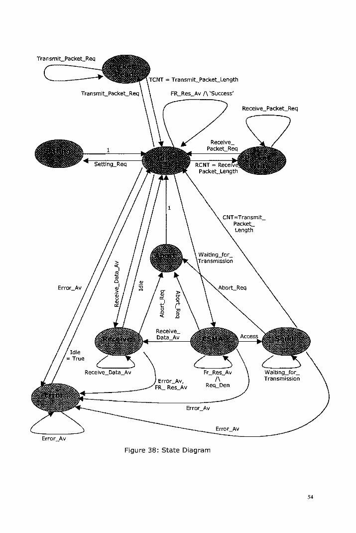
Tran smlCPackeCReq
Receive_ Data_Av
Figure 38: State Diagram
54
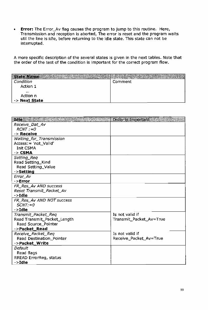
• Error: The Error_Av flag causes the program to jump to this routine. Here, Transmission and reception is aborted, The error is reset and the program waits util the line is idle, before returning to the idle state. This state can not be i nterru pted .
A more specific description of the several states is given in the next tables. Note that the order of the test of the condition is important for the correct program flow.
Condition Action 1
Action n -> Next State
Receive_DaCAv RCNT:=O
-> Receive Waitin9_for_ Transmission Access:= 'not_Valid'
Init CSMA -> CSM Settin9_Req Read Setting_Kind
Read Setting_Value -> Error_Av ->Error FR_Res_Av AND success Reset TransmiCPackeCAv ->Idle FR_Res_Av AND NOT success
SCNT:=O ->Idle TransmiCPackeCReq Read Transmit_Packet_Length
Read Sou rce_Poi nter ->Pac ad Receive_PackeCReq
Read Destination_Pointer -> Write Default
Read flags RREAD ErrorReg, status ->Idle
Comment
Is not valid if Transmit_Packet_Av=True
Is not valid if Receive_Packet_Av= True
55
Setting_Kind = 'Rate' RWRITE RateR, Setting_Value Set Setting_Req
->Idle Setting_Kind = 'NR'
RWRITE SettingR, Setting_Value Set Setting_Req
->Idle Setting_Kind = 'Mode'
RWRITE SettingR, Setting_Value Set Setti ng_Req
->Idle
CNT = TransmiLPackeLLength XCNT:=O
Set Transmit_Packet_Av Reset TransmiCPacket_Req
Set Waiting_for _Transmission ->Idle TransmiLPackeLReq
copy Mem (Source_Pointer+XCNT) > Transmit buffer(XCNT)
Inc XCNT ->P d
:1:iWI.'QtT~I :'~:\t!i:::!:\:!;::i:;£' ,1'.;,'
CNT =Receive_PackeLLength XCNT:=O
Reset Receive_Packet_Av Reset Receive_Packet_Req ->Idle Receive_PackeLReq
copy Receive buffer(XCNT)
':',':,,',.:;:::,
>Mem (Destination_Pointer+XCNT) Inc CNT
->Packet Write
Default RWRITE CMDReg, 'abort' Reset Abort_Req
->Idle
First time by SW, then by HW INT
,:W~ l:;;i;,:'{:Ji1!{ri',;L E::'::;:""";;':::;' ,.:,:::;:, , ,i,':,:''':
Line becomes Idle b its own
56
ErrocAv ->Error AborCReq ->Abort FR_Res_Av ->Error Receive_DaCAv
Copy Act_Data> Receive buffer(RCNT), Inc RCNT Reset Receive_Dat_Av RREAD StatusR, 'CRC'
->Receive CRC= 'OK' AND Idle
Set Receive_Packet_Av Receive_Packet_Length : = RCNT RCNT:=O
->Idle CRC<>'OK' AND Idle
RCNT:=O ->Idle Default ->Rece
ErrocAv ->Error AborCReq ->Abort Receive_DaCAv ->Receive FR_Res_Av AND 'Req_Denied'
RWRITE CMDReg, 'Reset_Req_Denied' Init CSMA
->CSMA Access = 'Valid'
SCNT:=O -> Default
« CSMA-Compute(Access) » ->CSMA
External collision detection
Retry CSMA
57
Error_Av V (FR_Res_Av /\ 'Collision,) Reset Access SCNT:=O
->Error AborCReq
Reset Access ->Abort SCNT = TransmiCPackeCLength
Reset Access SCNT:=O Reset Transmit_Packet_Av RWRITE CMDReg, 'EOF'
->Idle Waiting_for_ Transmission RWRITE DaraR, Transmit_Buffer (CNT)
INC CNT Reset Waiting_for_ Transmission
Default ->Send
;!i .... ,.~ Idle = TRUE ->Idle Error_A v
~
RWRITE CMDReg, Abort and reset errors Reset Error_Av
Reset FR_Res_Av ->Error Default RREAD StatusR, 'Idle' ->Error
Now wait for 'success' in
11l}"'""O,"'O",;;o,;,, ,,,qr ',,('\'(
58
8 Conclusions and recommendations
The project is started with collecting information about the LonTalk protocol. The most important conclusion that follows from the literature survey is that there is much literature about applications of the Lon protocol, but not much literature about the exact working or an implementation. Mostly, the protocol is not described in much detail. Therefore, to learn about a standard in detail, access to the standard document itself is necessary. As the Lon protocol is an open protocol since 1995 and the Echelon Company kept all information for itself (they sell the Neuron Chip), only few information is available before that period in the way of gUides, internal reports and data books. In the beginning, a possible implementation and good documentation about the protocol was available On Internet: 'LonTalk Protocol specification'. In 1998, a reference implementation is published by an independent company. When, in mid November 1999, the Protocol became an ANSI standard, it was not possible to download the article anymore as by paying for it (258 dollar!!!). Instead, article [R] was referred to, which was free to download.
Next, the design is started and implemented according to all information that was available. At the end some improvements can be done:
In the allocation of the Selection Code to the registers, the data in and data out register have a different selection code. It is possible to give these registers the same selection code, as this code has to be stored in the registers of the processor.
It is also possible to give the Command Register and the Status register the same Selection code. These registers will never be used at the same time and have an opposite information direction as well.
Finally, an example of the use of the designed LonTalk Interface Unit is written. In this example, many things are presented in a general way, leaving the exact implementation open.
Although chapter 7 is meant as an example implementation of the link layer protocol, in practice the transfer of a packet to the higher layer software would be done different. It is a better solution to use a FIFO and pointers to it, than copying the total packet to local buffers. This saves memory, as the packets are transferred directly and not via the buffers. In addition, copying the packet needs much time.
The shortest IDaSS simulation time for the designed unit is 158 11 seconds. So a frequency of 6 MHz achievable. If the unit is made with the 11J technology, it results in a factor 5 of improvement, as a rule of thumb. This means for the designed unit, that 60 MHz is achieved. This is within the protocol specifications. In practice, a higher frequency will be achieved, when the used expressions are optimized. This is not done for reasons of clarity.
59
Bibliography
[A] Siewiorekl D.P. and Swarz i R.S. THE THEORY AND PRACTICE OF RELIABLE SYSTEM DESIGN. Bedford: Digital Pressl 1982
[B] Berkvensl W.A.H. IMPLEMENTATION OF A BIT PROCESSOR AS PART OF A CONTROLLER AREA NETWORK PROTOCOL PROCESSOR. Eindhoven University of TechnologYI 1996 EB 625
[C] Gerritsenl B.H.H. DESIGN OF A TOKEN RING CONTROLLER IN IDASS. Eindhoven University of Technology EB 482
[lJ NEURON C PROGRAMMERS GUIDE. Palo Altol CA 943041 USAI Echelon Corporation, 1992. Ver.21 Part NR. 078-0002-011 doc. NR. 29300.
[2] LONMARK STANDARD Systemel Zeitschrift fur elektronikentwickler und systemintegratoren, Vol.121 19981 Iss. 41 p. 63-661 plaats ...
[3] Xie, C. et al A CASE STUDY ON THE DEVELOPMENT OF INTELLEGENT ACTUATOR COMPONENTS FOR DISTRIBUTED CONTROL SYSTEMS USING LONWORKS NEURON CHIPS. Mechatronicsi Vol. 8, 19981 No. 21 p. 103-1211 plaats .......
[4] Heusingerl P. et al OFFEN FUR JEDERMANN? DAS LONWORKS-PROTOKOLL UND EINE MOGLICHE IMPLEMENTIERUNG. Elektronikl Vol. 461 19971 Iss. 41 p. 56-64, Munchen.
[5] Stockl G. LON-TOOLS I SUPPORT FOR COMMISSIONING TOOLS FOR LONTALK COMMUNICATIONS PROTOCOL. Elektronikl Vol. 481 1999, Iss. 2, p. 66-69, Munchen.
[6] .t::i.ruml H. and Stockl G. REAL-TIME ENVIRONMENTI THE LONTALKS TECHNOLOGY Elektronik, Vol. 451 1996, Iss. 7, p. 62-68, Munchen.
[7J Thaller, K. et al INTEROPERABILITY OF ELECTRONIC INSTRUMENTS ON BUS SYSSTEMS - THE 'LONWORKS' STANDARD.
60
Elektronik, Vol. 44, 1995, Iss. 25, p. 66, 79-85, Munchen.
[8] Hollingum, J. LONWORKS, SOLUTIONS IN SIUCON. Assembly Automation, Vol. 14, 1994, 155.1, p.25-27, London.
[9] Nevill, B.M. et al LOCAL OPERATING NETWORKS - AN EMERGING TECHNOLOGY. Intellegent Instruments and Computers, Vol. 9, 1991,155.6, p. 203-211. Easthill, S.P
[K] LONTALK PROTOCOL. LonWorks engineering bulletin. Palo Alto, CA 94304, USA, Echelon Corporation, 1991. Part NR. 005-0017-01. www.echelon.com.
[Ll LONWORKS PROTOCOL LAYER 1 TIMING. Preliminary. Palo Alto, CA 94304, USA, Echelon Corporation, 1996. www.echelon.com.
[M] NODE BUILDER USER'S GUIDE. Palo Alto, CA 94304, USA, Echelon Corporation, 1995. Ver.3, Part NR. 078-0001-01, doc. NR. 1920. www.echelon.com.
[N] NEURON CHIP SPECIAL-PURPOSE MODE TRANSCEIVER INTERFACE SPECIFICATION. LonWorks engineering bulletin. Palo Alto, CA 94304, USA, Echelon Corporation, 1991. Part NR.? www.echelon.com.
[0] NEURON CHIP DATA BOOK. Motorola and Toshiba. No more specifications.
[P] LONWORKS TECHNOLOGY DEVICE DATA, DL 159/D. USA, Motorola, 1997. Rev.4, lATX31891-0
[Q] LONTALK PROTOCOL SPECIFICATIONS. Palo Alto, CA 94304, USA, Echelon Corporation, 1995. Ver.3, Part NR. 078-0125-01A (or ANSI/EIA 709.1-A-1999 now), www.global.his.com
[R] A C REFERENCE IMPLEMENTATION OF THE LONTALK PROTOCOL ON THE MC68360. Boca Raton, Florida, Adept Systems Incorporated, 1998. REV 1.7, www.adaptsystemsinc.com
61
[S] LON MARK 1-6 INTEROPERABILITY GUIDELINES. Palo Alto, CA 94304, USA, Echelon Corporation, 1995. Ver.3.0, Part NR. 078-0014-01. www.echelon.com.
[T] LONMARK APPLICATION LAYER INTEROPERABILITY GUIDELINES. Palo Alto, CA 94304, USA, Echelon Corporation, 1995. Ver.3, Part NR. 078-0120-01. www.echelon.com .
62