Embed Size (px)
Citation preview
Eindhoven University of Technology
BACHELOR
Characterization of self-assembled monolayers with FTIR and SE
Riberi, F.
Award date:2013
Link to publication
DisclaimerThis document contains a student thesis (bachelor's or master's), as authored by a student at Eindhoven University of Technology. Studenttheses are made available in the TU/e repository upon obtaining the required degree. The grade received is not published on the documentas presented in the repository. The required complexity or quality of research of student theses may vary by program, and the requiredminimum study period may vary in duration.
General rightsCopyright and moral rights for the publications made accessible in the public portal are retained by the authors and/or other copyright ownersand it is a condition of accessing publications that users recognise and abide by the legal requirements associated with these rights.
• Users may download and print one copy of any publication from the public portal for the purpose of private study or research. • You may not further distribute the material or use it for any profit-making activity or commercial gain

RIBERI François 2012/201
Technische Universiteit Eindhoven 1 ‘Applied Physics’ Department
Characterization of Self-assembled
Monolayers with FTIR and SE
Department of Applied Physics
Group Plasma and Materials Processing
Author :
François Riberi
Corrector :
Vincent Vandalon
Supervisors :
Vincent Vandalon
Erwin Kessels
Date :
February - June 2013
RIBERI François 2012/201
Technische Universiteit Eindhoven 2 ‘Applied Physics’ Department
Contents
I.Introduction .......................................................................................................................................... 4
Self-Assembled Monolayers ................................................................................................................ 8
Atomic Layer Deposition ..................................................................................................................... 9
II.Theoretical Background .................................................................................................................... 11
Nonlinear Optics ......................................................................................................................... 11
The Second Harmonic Generation (SHG) .................................................................................. 13
Spectroscopic Ellipsometry (SE) ................................................................................................ 14
Raman Spectroscopy ................................................................................................................. 17
III.Experimental Setup .......................................................................................................................... 19
Procedure synthesis of SAMs on Silicium .......................................................................................... 19
Samples description .......................................................................................................................... 22
ODTS and APTMS ............................................................................................................................... 22
IV.Experimental Results........................................................................................................................ 24
Octadecyltrichlorosilane (ODTS) ....................................................................................................... 24
FTIR absorption spectroscopy fingerprint ............................................................................. 24
Raman spectroscopy fingerprint ........................................................................................... 26
Spectroscopic Ellipsometry measurement and fitting procedure......................................... 27
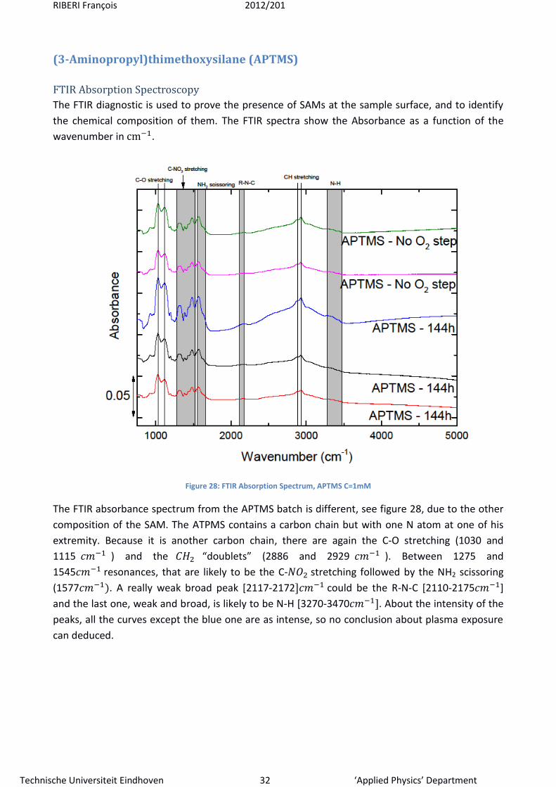
(3-Aminopropyl)thimethoxysilane (APTMS) ..................................................................................... 32
FTIR Absorption Spectroscopy............................................................................................... 32
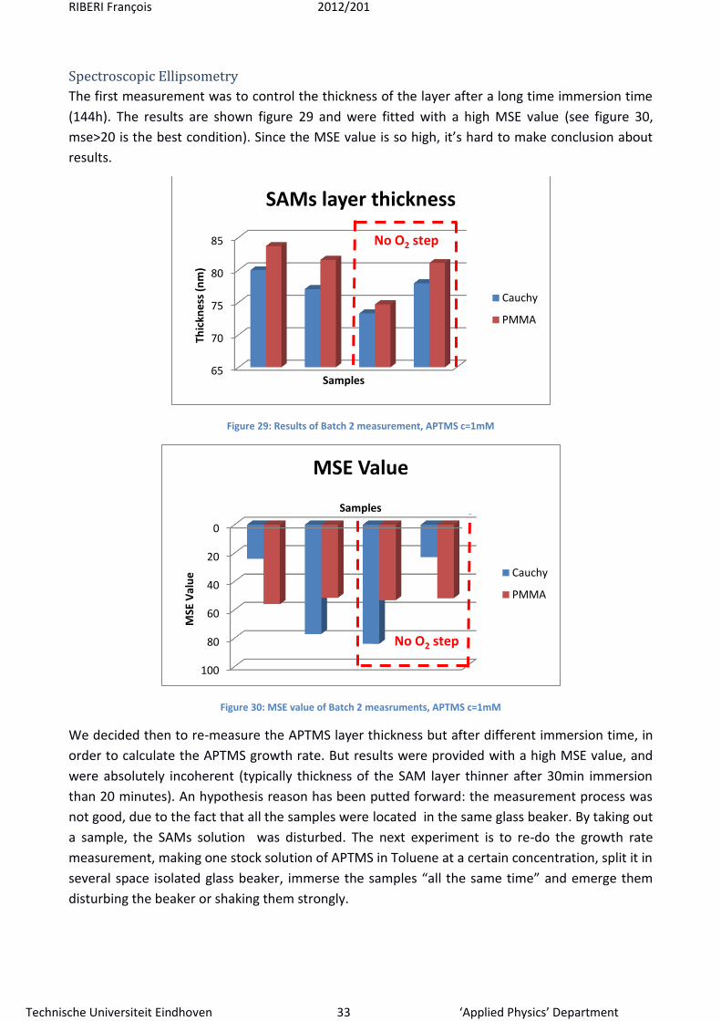
Spectroscopic Ellipsometry ................................................................................................... 33
Comparison ....................................................................................................................................... 34
V.Conclusion and discussion ................................................................................................................ 35
VI.Bibliography ..................................................................................................................................... 36
VII.Acknowledgements ......................................................................................................................... 37
RIBERI François 2012/201
Technische Universiteit Eindhoven 3 ‘Applied Physics’ Department
Abstract
Self-assembled monolayers (SAMs) offer a well defined, tailor made, surface with a range of
functional groups. These properties make the SAMs a nearly ideal surface as a test case for
the interface selective nonlinear optical technique of broadband sum-frequency generation.
Before the SAMs can be used as a test case, the films have to be characterized. The growth,
as well as the film properties of SAMs grown with Octadecyltrichlorosilane (ODTS) and (3-
Aminopropyl)thymetoxysilane (APTMS) precursors were investigated with spectroscopic
ellipsometry (SE) and infrared absorption spectroscopy(FTIR).
SAMs were grown on silicon Si(100) wafer containing a native oxide layer (SiO2), by wet
chemistry at atmospheric pressure (1,013 x 105 Pa) and ambient temperature (20°C). It is
well established in the literature that SAMs form in two steps: (1) the head clamping of the
active surface group of the SAM molecule, and (2) the self-assembling of the entire layer. To
functionalize the surface (remove Carbon contamination and leave OH group instead), an O2
plasma exposure has been performed at 80mTorr and 200°C. With FTIR the chemical
composition of the ODTS and APTMS films were determined. The thickness of the films was
characterized with SE. For the SE modelling, two different optical models were used and
compared. It was found that for the ODTS a single layer SAM is formed, whereas, for the
APTMS a multi-layer SAM can be grown. As a conclusion, FTIR and SE diagnostics are
relevant methods to characterize the SAMs studied here.
RIBERI François 2012/201
Technische Universiteit Eindhoven 4 ‘Applied Physics’ Department
I. Introduction
Nowadays, sustainable development has the wind in its sails. The driving forces behind the
development of sustainable technology is (1) an economic factor, due to the constant
increase of the oil price (2) An environmental factor, due to the increasing of the greenhouse
gases emissions. Numerous efforts are being made to find a solution to the energy issue.
Photovoltaic solar energy is seriously investigated as a solution from the last decades
through many research programs aiming for the improvement of the solar cells efficiency.
Energy Technology Perspectives (ETP) is the International Energy Agency’s most ambitious
publication on new developments in energy technology. It demonstrates how technologies –
from electric vehicles to smart grids – can make a decisive difference in achieving the
objective of limiting the global temperature rise to 2°C and enhancing energy security. The
need for sustainable energy sources is illustrated by the following quote from “Energy
Technology Perspectives 2012” [1]:
We must seize the opportunity for a clean energy future.
“Let me be straight: our ongoing failure to realise the full potential of clean
energy technology is alarming. Midway through 2012, energy demand and
prices are rising steadily, energy security concerns are at the forefront of
the political agenda, and energy-related carbon dioxide (CO2) emissions
have reached historic highs. Under current policies, both energy demand
and emissions are likely to double by 2050. [...] Policies can drive
technological innovation by stimulating investment in research,
development, demonstration and deployment. Policies can create market
frameworks that give these new technologies a fair chance to compete
against mature options. In short, policy can unleash the potential of
technology to ensure a sustainable energy future for our planet.”
Maria van der Hoeven, Executive Director
The executive director of the ETP 2012 writes, “Under current policies, both energy demand
and emissions are likely to double by 2050”. To combat the energy issue, several
technologies have emerged such as wind power, hydropower, solar energy (thermal and
photovoltaic) and biomass. Electricity as a power source offers a key advantage: it can be
precisely targeted to provide the right amount of energy at the right time to any end use. One inherent drawback of this technology is that its source (solar radiation) is intermittent
(alternating day / night). To make this viable, it is necessary to store the electricity. One
seriously studied solution is based on the use of hydrogen as a carrier and storage medium,
but its development will requires a significant amount of time. Because electricity is used
extensively in all sectors, the characteristics of electricity generation have important
implications for the entire economy. Tremendous potential exists to increase the use of
electricity for heat generation for industrial processes, for more efficient regulation of
RIBERI François 2012/201
Technische Universiteit Eindhoven 5 ‘Applied Physics’ Department
electric motors in industry, to power heat pumps for heating and cooling in buildings and
industry, and to support deployment of electric vehicles in transport. Clearly, promoting
greater use of electricity in such applications will increase demand for electricity. Whether
this increased demand of electricity leads to an increase in CO2 production, it greatly
depends on the energy-source mix that is used to generate electricity. It is, therefore,
important that sustainable methods for generating electricity are developed.
Photovoltaic, using solar energy as a sustainable solution.
Motivated by the interest for climate change and in view of the limited resources for energy,
electricity generation by photovoltaics (PV) is increasing in capacity worldwide [2]. The
merits of PV are obvious; it is silent, renewable and solar energy is the most abundant
source of energy on earth. Over the past decade, onshore wind has seen 27% average
annual growth, and solar photovoltaic (PV) has grown at 42%. Costs have fallen dramatically,
with a 75% reduction in solar PV system costs in as little as three years in some countries [3].
This augurs well for a promising and high developing future for PV. Historically, crystalline
silicon (c-Si) has been used as the light-absorbing semiconductor in most solar cells because
it yields stable solar cells with good efficiencies (15-17%) and uses process technology
developed from the huge knowledge base of the microelectronics industry. Two types of
crystalline silicon are used in the PV industry. The first is monocrystalline silicone, produced
by slicing wafers from a high-purity single crystal boule. The second is multicrystalline silicon,
made by sawing a cast block of silicon first into bars and then into wafers. But the high cost
of crystalline silicon wafers has led the industry to look at less expensive material to make
solar cells. The selected materials have all been strong light absorbers, and they only need to
be about 1 micron thick, so materials costs can be significantly reduced. The thin film solar
cell technology is increasing in capacity and market share and is now accounting for about
20% of the PV market. CdTe (Cadmium and Tellurium) solar cells represent about half and
the rest is divided between thin film silicon and (CGS) where the latter is
increasing rapidly.
Next step of solar photovoltaic cells: thin film solar cells?
Thin film solar cell industry is taking a larger share of the total photovoltaic market. The
reasons can be found in reduced production costs and increased efficiency. Currently, the
best thin film solar cells have above 19% efficiency and are based on the semiconductor alloy
material [4]. A new material, which earns an increasing interest, due to the
fact that it is made by abundant elements, is . This material is believed to
have many similarities to established (CIGS) cell design, but is still in an early
research phase.
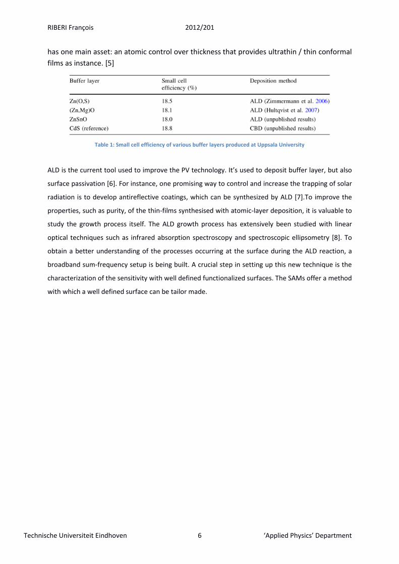
As can be seen on the table below, the deposition method used for the buffer layer of the
cells is Atomic Layer Deposition. This layer is sandwiched between two single-crystal
materials to accommodate difference in their crystallographic structures. The ALD technique
RIBERI François 2012/201
Technische Universiteit Eindhoven 6 ‘Applied Physics’ Department
has one main asset: an atomic control over thickness that provides ultrathin / thin conformal
films as instance. [5]
Table 1: Small cell efficiency of various buffer layers produced at Uppsala University
ALD is the current tool used to improve the PV technology. It’s used to deposit buffer layer, but also
surface passivation [6]. For instance, one promising way to control and increase the trapping of solar
radiation is to develop antireflective coatings, which can be synthesized by ALD [7].To improve the
properties, such as purity, of the thin-films synthesised with atomic-layer deposition, it is valuable to
study the growth process itself. The ALD growth process has extensively been studied with linear
optical techniques such as infrared absorption spectroscopy and spectroscopic ellipsometry [8]. To
obtain a better understanding of the processes occurring at the surface during the ALD reaction, a
broadband sum-frequency setup is being built. A crucial step in setting up this new technique is the
characterization of the sensitivity with well defined functionalized surfaces. The SAMs offer a method
with which a well defined surface can be tailor made.
RIBERI François 2012/201
Technische Universiteit Eindhoven 7 ‘Applied Physics’ Department
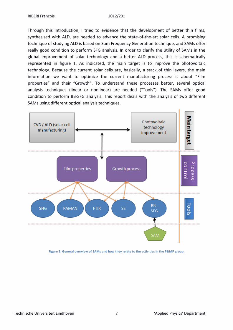
Through this introduction, I tried to evidence that the development of better thin films,
synthesised with ALD, are needed to advance the state-of-the-art solar cells. A promising
technique of studying ALD is based on Sum Frequency Generation technique, and SAMs offer
really good condition to perform SFG analysis. In order to clarify the utility of SAMs in the
global improvement of solar technology and a better ALD process, this is schematically
represented in figure 1. As indicated, the main target is to improve the photovoltaic
technology. Because the current solar cells are, basically, a stack of thin layers, the main
information we want to optimize the current manufacturing process is about “Film
properties” and their “Growth”. To understand these processes better, several optical
analysis techniques (linear or nonlinear) are needed (“Tools”). The SAMs offer good
condition to perform BB-SFG analysis. This report deals with the analysis of two different
SAMs using different optical analysis techniques.
Figure 1: General overview of SAMs and how they relate to the activities in the P&MP group.
RIBERI François 2012/201
Technische Universiteit Eindhoven 8 ‘Applied Physics’ Department
Self-Assembled Monolayers
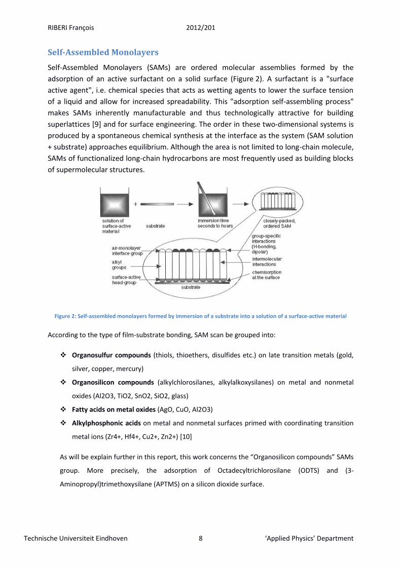
Self-Assembled Monolayers (SAMs) are ordered molecular assemblies formed by the
adsorption of an active surfactant on a solid surface (Figure 2). A surfactant is a "surface
active agent", i.e. chemical species that acts as wetting agents to lower the surface tension
of a liquid and allow for increased spreadability. This "adsorption self-assembling process"
makes SAMs inherently manufacturable and thus technologically attractive for building
superlattices [9] and for surface engineering. The order in these two-dimensional systems is
produced by a spontaneous chemical synthesis at the interface as the system (SAM solution
+ substrate) approaches equilibrium. Although the area is not limited to long-chain molecule,
SAMs of functionalized long-chain hydrocarbons are most frequently used as building blocks
of supermolecular structures.
Figure 2: Self-assembled monolayers formed by immersion of a substrate into a solution of a surface-active material
According to the type of film-substrate bonding, SAM scan be grouped into:
Organosulfur compounds (thiols, thioethers, disulfides etc.) on late transition metals (gold,
silver, copper, mercury)
Organosilicon compounds (alkylchlorosilanes, alkylalkoxysilanes) on metal and nonmetal
oxides (Al2O3, TiO2, SnO2, SiO2, glass)
Fatty acids on metal oxides (AgO, CuO, Al2O3)
Alkylphosphonic acids on metal and nonmetal surfaces primed with coordinating transition
metal ions (Zr4+, Hf4+, Cu2+, Zn2+) [10]
As will be explain further in this report, this work concerns the “Organosilicon compounds” SAMs
group. More precisely, the adsorption of Octadecyltrichlorosilane (ODTS) and (3-
Aminopropyl)trimethoxysilane (APTMS) on a silicon dioxide surface.
RIBERI François 2012/201
Technische Universiteit Eindhoven 9 ‘Applied Physics’ Department
Atomic Layer Deposition
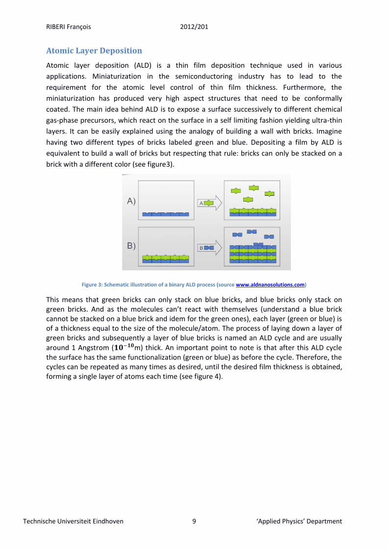
Atomic layer deposition (ALD) is a thin film deposition technique used in various
applications. Miniaturization in the semiconductoring industry has to lead to the
requirement for the atomic level control of thin film thickness. Furthermore, the
miniaturization has produced very high aspect structures that need to be conformally
coated. The main idea behind ALD is to expose a surface successively to different chemical
gas-phase precursors, which react on the surface in a self limiting fashion yielding ultra-thin
layers. It can be easily explained using the analogy of building a wall with bricks. Imagine
having two different types of bricks labeled green and blue. Depositing a film by ALD is
equivalent to build a wall of bricks but respecting that rule: bricks can only be stacked on a
brick with a different color (see figure3).
Figure 3: Schematic illustration of a binary ALD process (source www.aldnanosolutions.com)
This means that green bricks can only stack on blue bricks, and blue bricks only stack on green bricks. And as the molecules can’t react with themselves (understand a blue brick cannot be stacked on a blue brick and idem for the green ones), each layer (green or blue) is of a thickness equal to the size of the molecule/atom. The process of laying down a layer of green bricks and subsequently a layer of blue bricks is named an ALD cycle and are usually around 1 Angstrom ( m) thick. An important point to note is that after this ALD cycle the surface has the same functionalization (green or blue) as before the cycle. Therefore, the cycles can be repeated as many times as desired, until the desired film thickness is obtained, forming a single layer of atoms each time (see figure 4).
RIBERI François 2012/201
Technische Universiteit Eindhoven 10 ‘Applied Physics’ Department
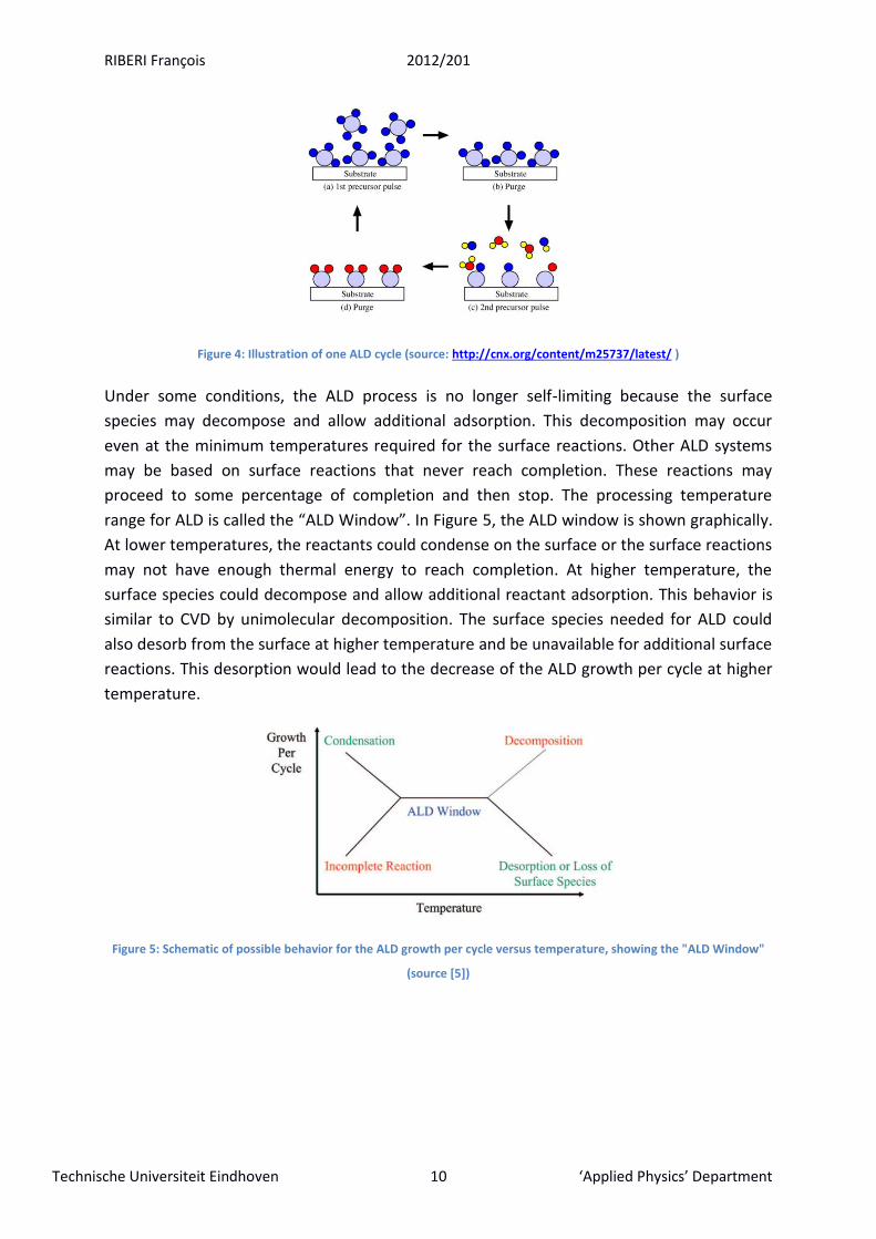
Figure 4: Illustration of one ALD cycle (source: http://cnx.org/content/m25737/latest/ )
Under some conditions, the ALD process is no longer self-limiting because the surface
species may decompose and allow additional adsorption. This decomposition may occur
even at the minimum temperatures required for the surface reactions. Other ALD systems
may be based on surface reactions that never reach completion. These reactions may
proceed to some percentage of completion and then stop. The processing temperature
range for ALD is called the “ALD Window”. In Figure 5, the ALD window is shown graphically.
At lower temperatures, the reactants could condense on the surface or the surface reactions
may not have enough thermal energy to reach completion. At higher temperature, the
surface species could decompose and allow additional reactant adsorption. This behavior is
similar to CVD by unimolecular decomposition. The surface species needed for ALD could
also desorb from the surface at higher temperature and be unavailable for additional surface
reactions. This desorption would lead to the decrease of the ALD growth per cycle at higher
temperature.
Figure 5: Schematic of possible behavior for the ALD growth per cycle versus temperature, showing the "ALD Window"
(source [5])
RIBERI François 2012/201
Technische Universiteit Eindhoven 11 ‘Applied Physics’ Department
II. Theoretical Background
In this part, the theoretical explanation is given, needed to understand what are the different
technology used and how do they work. First, the nonlinear optics, necessary to understand
BroadBand Sum Frequency Generation (BBSFG) and Second Harmonic Generation (SHG)
mechanisms will be discussed. Then, the three optical diagnostic techniques used through this
project will be explained, namely FTIR absorption spectroscopy, Raman spectroscopy and
Ellipsometry spectroscopy (SE).
Nonlinear Optics
Basically, two major theoretical approaches can be employed in nonlinear optics: the “semi-
classical” theory (SMT) and the “quantum electrodynamical” (QET) theory. The main feature of the
SMT theory is that the media composed of atoms or molecules are described by a theory of
quantum mechanics, while the light radiation is described by the classical Maxwell’s theory. The
main issue of this method is to give the expressions of macroscopic nonlinear electric polarization
for optical media. On the other hand, the QET theory treats the medium and optical field as
combined and quantized system, both the medium and optical field should be described in the
way of quantum mechanics. As a result, the wave function of the combined system is expressed as
the product of two specific functions: {molecular system} *{quantized photon field}. It should be
pointed that there is no major contradiction between the results and conclusions given by these
two methods, and they can give the same quantitative results in many case (cross section of
Raman scattering or cross section of two-photon absorption). Nevertheless, there are many well
known examples that have shown the advantage of the QET over the SMT [11]. The most
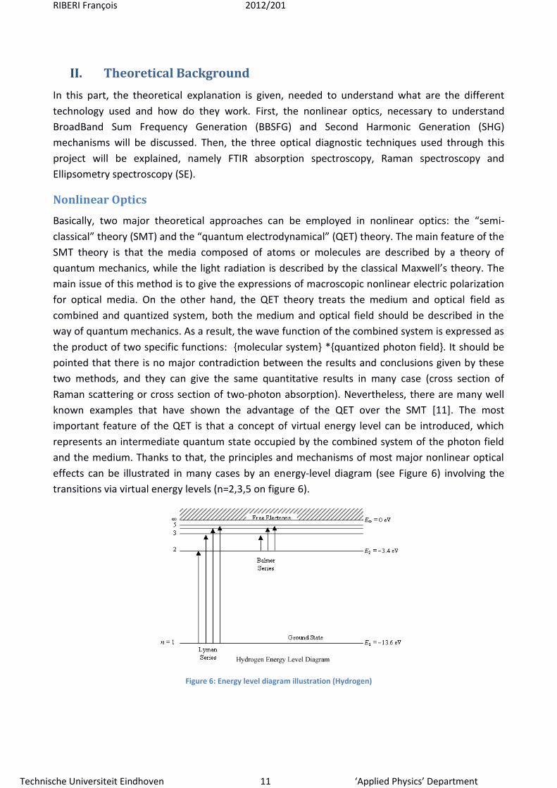
important feature of the QET is that a concept of virtual energy level can be introduced, which
represents an intermediate quantum state occupied by the combined system of the photon field
and the medium. Thanks to that, the principles and mechanisms of most major nonlinear optical
effects can be illustrated in many cases by an energy-level diagram (see Figure 6) involving the
transitions via virtual energy levels (n=2,3,5 on figure 6).
Figure 6: Energy level diagram illustration (Hydrogen)
RIBERI François 2012/201
Technische Universiteit Eindhoven 12 ‘Applied Physics’ Department
A lot of different effects are used in nonlinear optics, and two of them are detailed in that report:
Broad-Bandwidth Sum-Frequency Generation (BBSFG), and Second Harmonic Generation (SHG
also called frequency doubling).
Before going more into details, I think useful to clarify why do we talk about linear and nonlinear
optic. Light is an electromagnetic wave, when it crosses a material, the light is going to modify the
state of the material, i.e the polarization of the material. As long as the wave is not very intense,
this polarization can be considered as proportional to the incidental wave power: i.e linear
behavior.
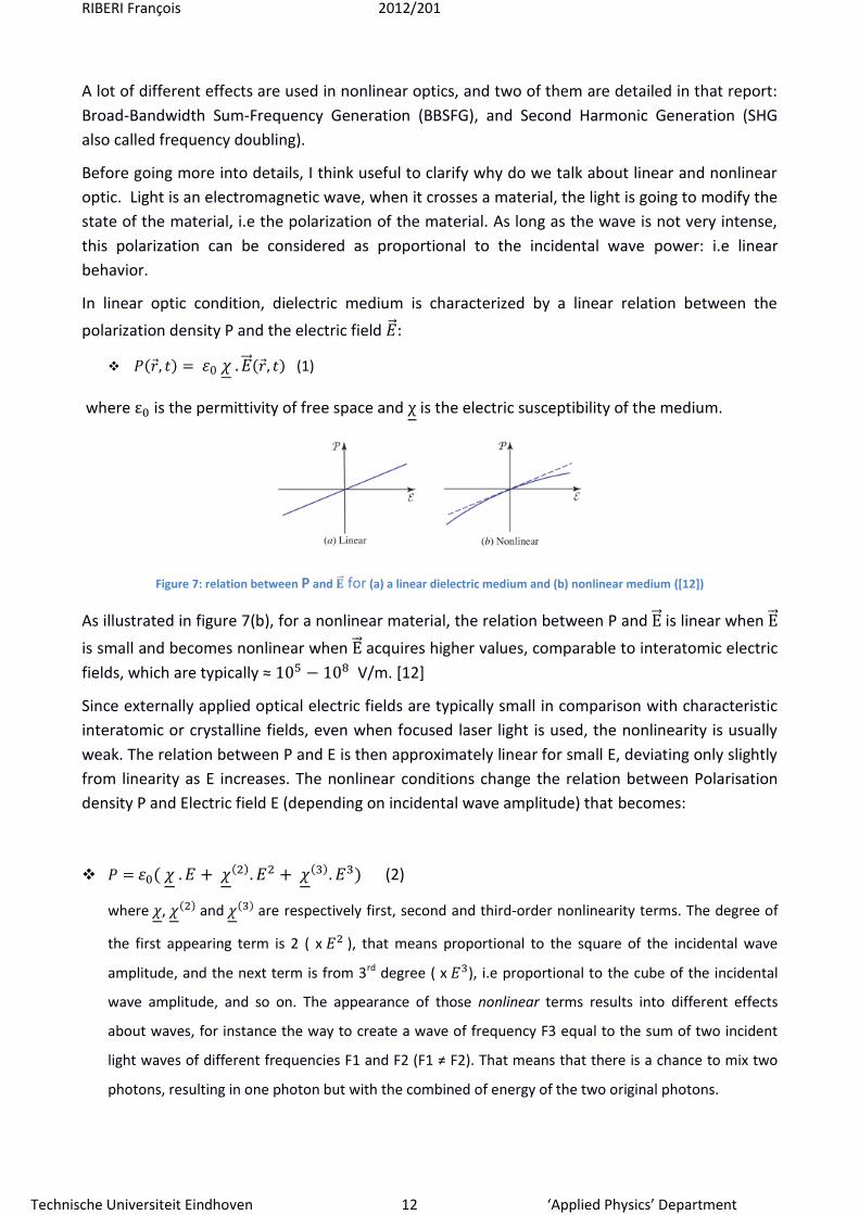
In linear optic condition, dielectric medium is characterized by a linear relation between the
polarization density P and the electric field
(1)
where is the permittivity of free space and is the electric susceptibility of the medium.
Figure 7: relation between P and for (a) a linear dielectric medium and (b) nonlinear medium ([12])
As illustrated in figure 7(b), for a nonlinear material, the relation between P and is linear when
is small and becomes nonlinear when acquires higher values, comparable to interatomic electric
fields, which are typically ≈ V/m. [12]
Since externally applied optical electric fields are typically small in comparison with characteristic
interatomic or crystalline fields, even when focused laser light is used, the nonlinearity is usually
weak. The relation between P and E is then approximately linear for small E, deviating only slightly
from linearity as E increases. The nonlinear conditions change the relation between Polarisation
density P and Electric field E (depending on incidental wave amplitude) that becomes:
(2)
where , and are respectively first, second and third-order nonlinearity terms. The degree of
the first appearing term is 2 ( x ), that means proportional to the square of the incidental wave
amplitude, and the next term is from 3rd degree ( x ), i.e proportional to the cube of the incidental
wave amplitude, and so on. The appearance of those nonlinear terms results into different effects
about waves, for instance the way to create a wave of frequency F3 equal to the sum of two incident
light waves of different frequencies F1 and F2 (F1 ≠ F2). That means that there is a chance to mix two
photons, resulting in one photon but with the combined of energy of the two original photons.
RIBERI François 2012/201
Technische Universiteit Eindhoven 13 ‘Applied Physics’ Department
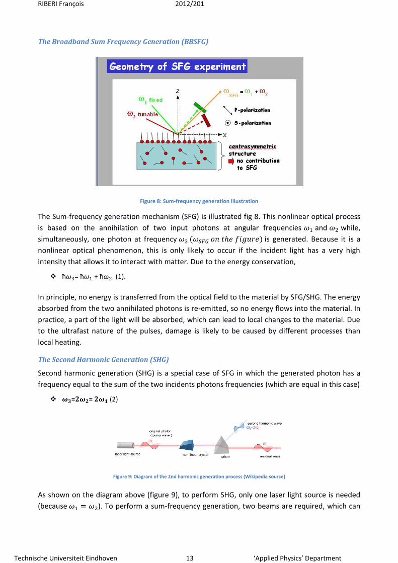
The Broadband Sum Frequency Generation (BBSFG)
Figure 8: Sum-frequency generation illustration
The Sum-frequency generation mechanism (SFG) is illustrated fig 8. This nonlinear optical process
is based on the annihilation of two input photons at angular frequencies and while,
simultaneously, one photon at frequency is generated. Because it is a
nonlinear optical phenomenon, this is only likely to occur if the incident light has a very high
intensity that allows it to interact with matter. Due to the energy conservation,
ħ = ħ + ħ (1).
In principle, no energy is transferred from the optical field to the material by SFG/SHG. The energy
absorbed from the two annihilated photons is re-emitted, so no energy flows into the material. In
practice, a part of the light will be absorbed, which can lead to local changes to the material. Due
to the ultrafast nature of the pulses, damage is likely to be caused by different processes than
local heating.
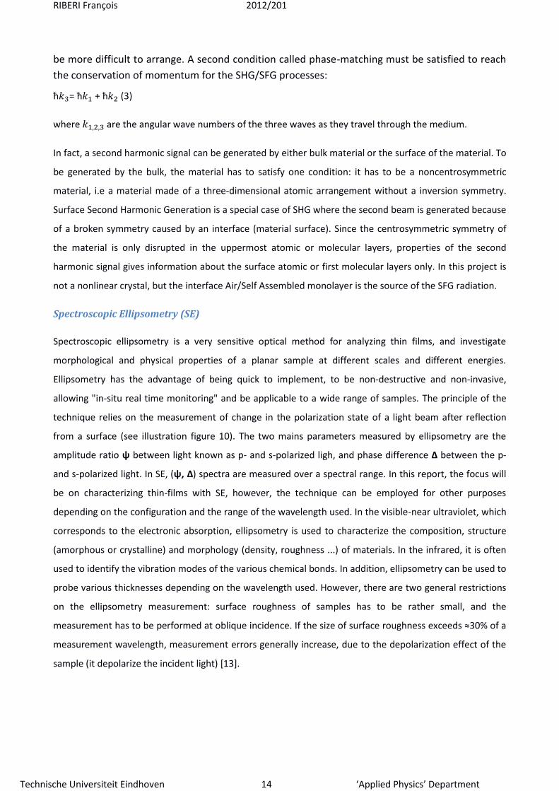
The Second Harmonic Generation (SHG)
Second harmonic generation (SHG) is a special case of SFG in which the generated photon has a
frequency equal to the sum of the two incidents photons frequencies (which are equal in this case)
= = (2)
Figure 9: Diagram of the 2nd harmonic generation process (Wikipedia source)
As shown on the diagram above (figure 9), to perform SHG, only one laser light source is needed
(because ). To perform a sum-frequency generation, two beams are required, which can
RIBERI François 2012/201
Technische Universiteit Eindhoven 14 ‘Applied Physics’ Department
be more difficult to arrange. A second condition called phase-matching must be satisfied to reach
the conservation of momentum for the SHG/SFG processes:
ħ = ħ + ħ (3)
where are the angular wave numbers of the three waves as they travel through the medium.
In fact, a second harmonic signal can be generated by either bulk material or the surface of the material. To
be generated by the bulk, the material has to satisfy one condition: it has to be a noncentrosymmetric
material, i.e a material made of a three-dimensional atomic arrangement without a inversion symmetry.
Surface Second Harmonic Generation is a special case of SHG where the second beam is generated because
of a broken symmetry caused by an interface (material surface). Since the centrosymmetric symmetry of
the material is only disrupted in the uppermost atomic or molecular layers, properties of the second
harmonic signal gives information about the surface atomic or first molecular layers only. In this project is
not a nonlinear crystal, but the interface Air/Self Assembled monolayer is the source of the SFG radiation.
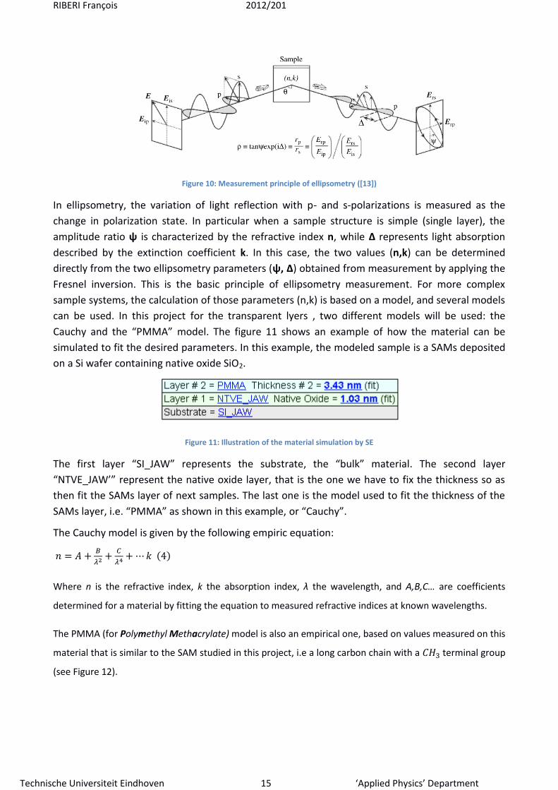
Spectroscopic Ellipsometry (SE)
Spectroscopic ellipsometry is a very sensitive optical method for analyzing thin films, and investigate
morphological and physical properties of a planar sample at different scales and different energies.
Ellipsometry has the advantage of being quick to implement, to be non-destructive and non-invasive,
allowing "in-situ real time monitoring" and be applicable to a wide range of samples. The principle of the
technique relies on the measurement of change in the polarization state of a light beam after reflection
from a surface (see illustration figure 10). The two mains parameters measured by ellipsometry are the
amplitude ratio ψ between light known as p- and s-polarized ligh, and phase difference Δ between the p-
and s-polarized light. In SE, (ψ, Δ) spectra are measured over a spectral range. In this report, the focus will
be on characterizing thin-films with SE, however, the technique can be employed for other purposes
depending on the configuration and the range of the wavelength used. In the visible-near ultraviolet, which
corresponds to the electronic absorption, ellipsometry is used to characterize the composition, structure
(amorphous or crystalline) and morphology (density, roughness ...) of materials. In the infrared, it is often
used to identify the vibration modes of the various chemical bonds. In addition, ellipsometry can be used to
probe various thicknesses depending on the wavelength used. However, there are two general restrictions
on the ellipsometry measurement: surface roughness of samples has to be rather small, and the
measurement has to be performed at oblique incidence. If the size of surface roughness exceeds ≈30% of a
measurement wavelength, measurement errors generally increase, due to the depolarization effect of the
sample (it depolarize the incident light) [13].
RIBERI François 2012/201
Technische Universiteit Eindhoven 15 ‘Applied Physics’ Department
Figure 10: Measurement principle of ellipsometry ([13])
In ellipsometry, the variation of light reflection with p- and s-polarizations is measured as the
change in polarization state. In particular when a sample structure is simple (single layer), the
amplitude ratio ψ is characterized by the refractive index n, while Δ represents light absorption
described by the extinction coefficient k. In this case, the two values (n,k) can be determined
directly from the two ellipsometry parameters (ψ, Δ) obtained from measurement by applying the
Fresnel inversion. This is the basic principle of ellipsometry measurement. For more complex
sample systems, the calculation of those parameters (n,k) is based on a model, and several models
can be used. In this project for the transparent lyers , two different models will be used: the
Cauchy and the “PMMA” model. The figure 11 shows an example of how the material can be
simulated to fit the desired parameters. In this example, the modeled sample is a SAMs deposited
on a Si wafer containing native oxide SiO2.
Figure 11: Illustration of the material simulation by SE
The first layer “SI_JAW” represents the substrate, the “bulk” material. The second layer
“NTVE_JAW’” represent the native oxide layer, that is the one we have to fix the thickness so as
then fit the SAMs layer of next samples. The last one is the model used to fit the thickness of the
SAMs layer, i.e. “PMMA” as shown in this example, or “Cauchy”.
The Cauchy model is given by the following empiric equation:
Where n is the refractive index, k the absorption index, λ the wavelength, and A,B,C… are coefficients
determined for a material by fitting the equation to measured refractive indices at known wavelengths.
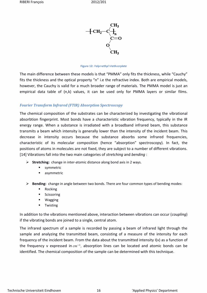
The PMMA (for Polymethyl Methacrylate) model is also an empirical one, based on values measured on this
material that is similar to the SAM studied in this project, i.e a long carbon chain with a terminal group
(see Figure 12).
RIBERI François 2012/201
Technische Universiteit Eindhoven 16 ‘Applied Physics’ Department
Figure 12: Polymethyl Methacrylate
The main difference between these models is that “PMMA” only fits the thickness, while “Cauchy”
fits the thickness and the optical property “n” i.e the refractive index. Both are empirical models,
however, the Cauchy is valid for a much broader range of materials. The PMMA model is just an
empirical data table of (n,k) values, it can be used only for PMMA layers or similar films.
Fourier Transform Infrared (FTIR) Absorption Spectroscopy
The chemical composition of the substrates can be characterized by investigating the vibrational
absorbtion fingerprint. Most bonds have a characteristic vibration frequency, typically in the IR
energy range. When a substance is irradiated with a broadband infrared beam, this substance
transmits a beam which intensity is generally lower than the intensity of the incident beam. This
decrease in intensity occurs because the substance absorbs some infrared frequencies,
characteristic of its molecular composition (hence “absorption” spectroscopy). In fact, the
positions of atoms in molecules are not fixed, they are subject to a number of different vibrations.
[14] Vibrations fall into the two main categories of stretching and bending :
Stretching: change in inter-atomic distance along bond axis in 2 ways.
symmetric
asymmetric
Bending: change in angle between two bonds. There are four common types of bending modes:
Rocking
Scissoring
Wagging
Twisting
In addition to the vibrations mentioned above, interaction between vibrations can occur (coupling)
if the vibrating bonds are joined to a single, central atom.
The infrared spectrum of a sample is recorded by passing a beam of infrared light through the
sample and analyzing the transmitted beam, consisting of a measure of the intensity for each
frequency of the incident beam. From the data about the transmitted intensity I(ν) as a function of
the frequency ν expressed in , absorption lines can be located and atomic bonds can be
identified. The chemical composition of the sample can be determined with this technique.
RIBERI François 2012/201
Technische Universiteit Eindhoven 17 ‘Applied Physics’ Department
Raman Spectroscopy
Raman spectroscopy is a non-destructive spectroscopy used to characterize molecular
composition and external structure of a material[15]. In practice, monochromatic light is focussed
on the sample and the scattered light is first being collected by a lens, then sent through a
monochromator to measure its intensity by a detector (CCD type). Raman is the inelastic
scattering of monochromatic light that means frequency of photons in monochromatic light
changes upon interaction with a sample. Photons from a laser light are absorbed by the sample
and then reemitted, and the frequency of the reemitted photons is shifted up or down in
comparison with original monochromatic frequency. This is called the Raman effect and provides
information about vibrational, rotational and other low frequency transitions in molecules. A
molecule with no Raman-active modes absorbs a photon with the frequency , it passes in an
« excited mode», and re-emit exactly the same photon moving at the same frequency during its
desexcitation to basic vibrational state. This type of interaction is called an elastic Rayleigh
scattering. About 99.999% of all incident photons in spontaneous Raman undergo elastic Rayleigh
scattering. This type of signal is useless for practical purposes of molecular characterization. Only
about 0.001% of the incident light produces inelastic Raman signal, therefore special measures are
required to distinguish it from the predominant Rayleigh scattering. Instruments such as notch
filters, tuneable filters, laser stop apertures, double and triple spectrometric systems are used to
reduce Rayleigh scattering and obtain high-quality Raman spectra. One simple way to improve
Raman signal Intensity is scaling (up) the laser power, because the intensity of the signal analyzed
is proportional to the square of the electric field (relative to the incident wave intensity). But by
scaling up too much the incident intensity, a condition can be reached where the incident beam
will locally change the material analyzed (for instance with amorphous silicon, it locally melts and
crystallizes the silicon). So the best conditions are a compromise between the Signal-to-Noise ratio
and incident light altering the material. Raman spectroscopy can be used to study solid, liquid and
gaseous samples.

RIBERI François 2012/201
Technische Universiteit Eindhoven 19 ‘Applied Physics’ Department
III. Experimental Setup
In this part is given details about the experimental conditions. First about the manufacturing
process of the SAMs is discussed. Then a detailed description is shown of each SAMs, i.e ODTS and
APTMS, and each conditions respected during their manufacturing..
Procedure synthesis of SAMs on Silicium
The aim is to grow Self Assembled Monolayers (SAMs) on a silicon (100) wafer with native oxide.
Our SAMs are typically made of a chain of C atoms side-terminated with H atoms, the head of the
SAM contains Silane. The silane head is the attachment point of the molecule on the substrate
surface. To allow the attachment of the molecule, to start the growth and the self organization of
the SAMS, the substrate has to have a hydroxyl (OH group) termination. The OH functionalization
is achieved by a O2 plasma exposure to the untreated Si(100) wafers with native-oxide. The aim of
the plasma is to use the energy of the excited atoms to remove carbon like surface contamination
and to form the OH groups from ambient water. The typical parameters of the O2 plasma step are
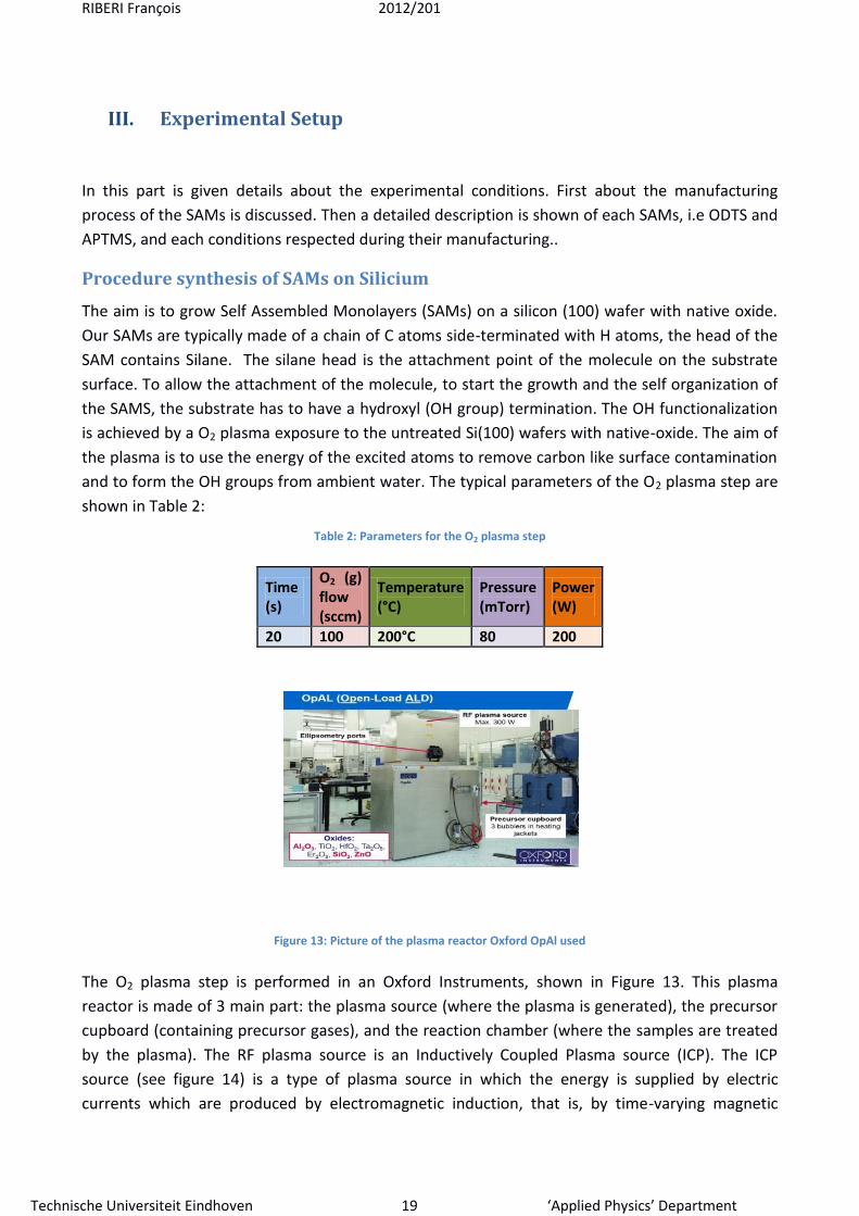
shown in Table 2:
Table 2: Parameters for the O2 plasma step
Time (s)
O2 (g) flow (sccm)
Temperature (°C)
Pressure (mTorr)
Power (W)
20 100 200°C 80 200
Figure 13: Picture of the plasma reactor Oxford OpAl used
The O2 plasma step is performed in an Oxford Instruments, shown in Figure 13. This plasma
reactor is made of 3 main part: the plasma source (where the plasma is generated), the precursor
cupboard (containing precursor gases), and the reaction chamber (where the samples are treated
by the plasma). The RF plasma source is an Inductively Coupled Plasma source (ICP). The ICP
source (see figure 14) is a type of plasma source in which the energy is supplied by electric
currents which are produced by electromagnetic induction, that is, by time-varying magnetic

RIBERI François 2012/201
Technische Universiteit Eindhoven 20 ‘Applied Physics’ Department
fields. By going along the coil, the current induces a time-varying magnetic field that is applied to
the gas molecule present in the volume inside the coil. The molecule moves and collapse between
them that result in an ionization process. The plasma is generated and maintained due to that
mechanism, i.e. inelastic collision between molecules/atoms of a gas.
Figure 14: Illustration of an ICP source
ICP discharges are of relatively high electron density, on the order of 1015 cm−3 and have wide
applications where high-density plasma is needed. One advantage of this plasma processing mode
is the wafer location’s, away from plasma, and hence avoid direct plasma exposure. Desired
reactions (e.g. etching) are implemented by extracting ionized species from the plasma generation
region and directing them toward to the wafer. The advantage of remote plasma process results in
less surface damage than standard process, since plasma generated ions are energetically relaxed
arriving at the surface of the wafer.

RIBERI François 2012/201
Technische Universiteit Eindhoven 22 ‘Applied Physics’ Department
Sample description
ODTS and APTMS
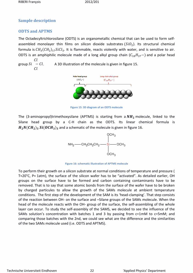
The Octadecyltrichlorosilane (ODTS) is an organometallic chemical that can be used to form self-
assembled monolayer thin films on silicon dioxide substrates ). Its structural chemical
formula is . It is flammable, reacts violently with water, and is sensitive to air.
ODTS is an amphiphilic molecule made of a long alkyl group chain ( and a polar head
group
. A 3D illustration of the molecule is given in figure 15.
Figure 15: 3D diagram of an ODTS molecule
The (3-aminopropyl)trimethoxysilane (APTMS) is starting from a molecule, linked to the
Silane head group by a C-H chain as the ODTS. Its linear chemical formula is
and a schematic of the molecule is given in figure 16.
Figure 16: schematic illustration of APTMS molecule
To perform their growth on a silicon substrate at normal conditions of temperature and pressure ( T≈20°C, P≈ 1atm), the surface of the silicon wafer has to be “activated”. As detailed earlier, OH groups on the surface have to be formed and carbon containing contaminants have to be removed. That is to say that some atomic bonds from the surface of the wafer have to be broken by charged particules to allow the growth of the SAMs molecule at ambient temperature conditions. The first step of the development of the SAM is its ‘head-clamping’. That step consists of the reaction between OH- on the surface and –Silane groups of the SAMs molecule. When the head of the molecule reacts with the OH- group of the surface, the self-assembling of the whole layer can occur. To study the self-assembly of the SAMS, we decided to see the influence of the SAMs solution’s concentration with batches 1 and 3 by passing from c=1mM to c=5mM; and comparing those batches with the 2nd, we could see what are the difference and the similarities of the two SAMs molecule used (i.e. ODTS and APTMS).
RIBERI François 2012/201
Technische Universiteit Eindhoven 23 ‘Applied Physics’ Department
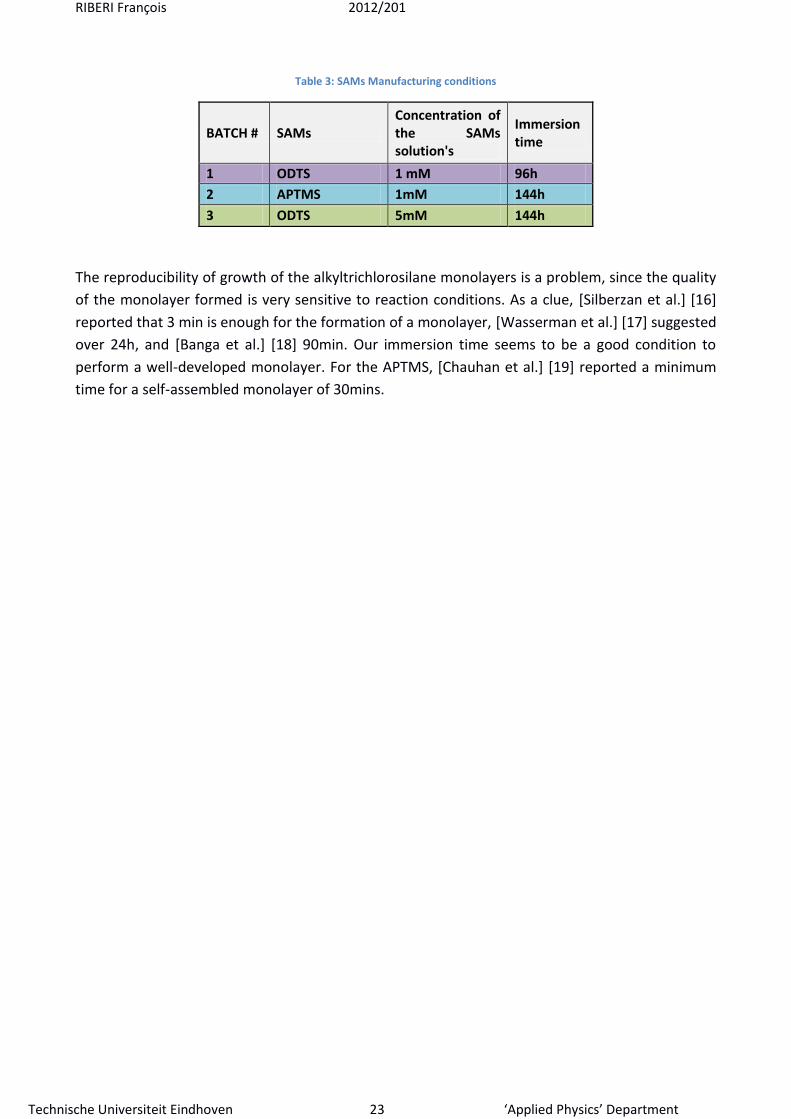
Table 3: SAMs Manufacturing conditions
BATCH # SAMs Concentration of the SAMs solution's
Immersion time
1 ODTS 1 mM 96h
2 APTMS 1mM 144h
3 ODTS 5mM 144h
The reproducibility of growth of the alkyltrichlorosilane monolayers is a problem, since the quality
of the monolayer formed is very sensitive to reaction conditions. As a clue, [Silberzan et al.] [16]
reported that 3 min is enough for the formation of a monolayer, [Wasserman et al.] [17] suggested
over 24h, and [Banga et al.] [18] 90min. Our immersion time seems to be a good condition to
perform a well-developed monolayer. For the APTMS, [Chauhan et al.] [19] reported a minimum
time for a self-assembled monolayer of 30mins.
RIBERI François 2012/201
Technische Universiteit Eindhoven 24 ‘Applied Physics’ Department
IV. Experimental Results
Here are presented the different results and graphs about each SAM molecule. The first
part shows the results relative to ODTS, the second part about APTMS, and the last one shows a
comparison between them.
Octadecyltrichlorosilane (ODTS)
FTIR absorption spectroscopy fingerprint
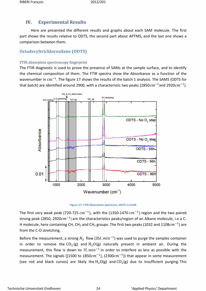
The FTIR diagnostic is used to prove the presence of SAMs at the sample surface, and to identify
the chemical composition of them. The FTIR spectra show the Absorbance as a function of the
wavenumber in . The figure 17 shows the results of the batch 1 analysis. The SAMS (ODTS for
that batch) are identified around 2900, with a characteristic two peaks (2850 and 2920 ).
Figure 17: FTIR Absorption Spectrum, ODTS C=1mM
The first very weak peak (720-725 , with the (1350-1470 region and the two paired
strong peak (2850, 2920 ) are the characteristics peaks/region of an Alkane molecule, i.e a C-
H molecule, here containing CH, CH2 and CH3 groups. The first two peaks (1032 and 1108 ) are
from the C-O stretching.
Before the measurement, a strong flow (35 ) was used to purge the samples container
in order to remove the (g) and (g) naturally present in ambient air. During the
measurement, this flow is down to 7 in order to interfere as less as possible with the
measurement. The signals ([1500 to 1850 ], (2300 )) that appear in some measurement
(see red and black curves) are likely the (g) and (g) due to insufficient purging This
RIBERI François 2012/201
Technische Universiteit Eindhoven 25 ‘Applied Physics’ Department
hypothesis is strengthened by the fact that both the CO2(g) and the (g) are present at the
same time to the same degree.
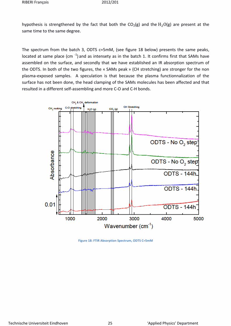
The spectrum from the batch 3, ODTS c=5mM, (see figure 18 below) presents the same peaks,
located at same place (cm -1) and as intensety as in the batch 1. It confirms first that SAMs have
assembled on the surface, and secondly that we have established an IR absorption spectrum of
the ODTS. In both of the two figures, the « SAMs peak » (CH stretching) are stronger for the non
plasma-exposed samples. A speculation is that because the plasma functionnalization of the
surface has not been done, the head clamping of the SAMs molecules has been affected and that
resulted in a different self-assembling and more C-O and C-H bonds.
Figure 18: FTIR Absorption Spectrum, ODTS C=5mM
RIBERI François 2012/201
Technische Universiteit Eindhoven 26 ‘Applied Physics’ Department
Raman spectroscopy fingerprint
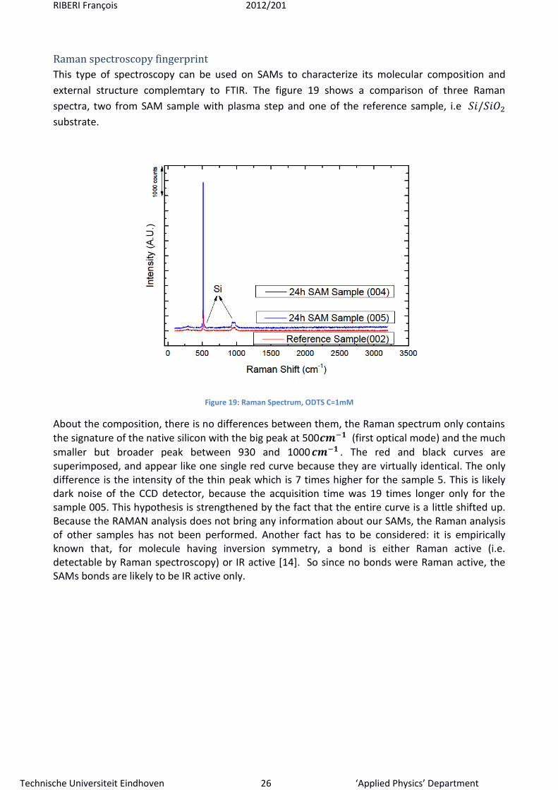
This type of spectroscopy can be used on SAMs to characterize its molecular composition and
external structure complemtary to FTIR. The figure 19 shows a comparison of three Raman
spectra, two from SAM sample with plasma step and one of the reference sample, i.e
substrate.
Figure 19: Raman Spectrum, ODTS C=1mM
About the composition, there is no differences between them, the Raman spectrum only contains the signature of the native silicon with the big peak at 500 (first optical mode) and the much
smaller but broader peak between 930 and 1000 . The red and black curves are superimposed, and appear like one single red curve because they are virtually identical. The only difference is the intensity of the thin peak which is 7 times higher for the sample 5. This is likely dark noise of the CCD detector, because the acquisition time was 19 times longer only for the sample 005. This hypothesis is strengthened by the fact that the entire curve is a little shifted up. Because the RAMAN analysis does not bring any information about our SAMs, the Raman analysis of other samples has not been performed. Another fact has to be considered: it is empirically known that, for molecule having inversion symmetry, a bond is either Raman active (i.e. detectable by Raman spectroscopy) or IR active [14]. So since no bonds were Raman active, the SAMs bonds are likely to be IR active only.
RIBERI François 2012/201
Technische Universiteit Eindhoven 27 ‘Applied Physics’ Department
Spectroscopic Ellipsometry measurement and fitting procedure
This type of spectroscopy is used to determine the thickness of the layer deposited, with a
nanometer scale precision, as well as optical properties (n,k) depending on the fitting model used.
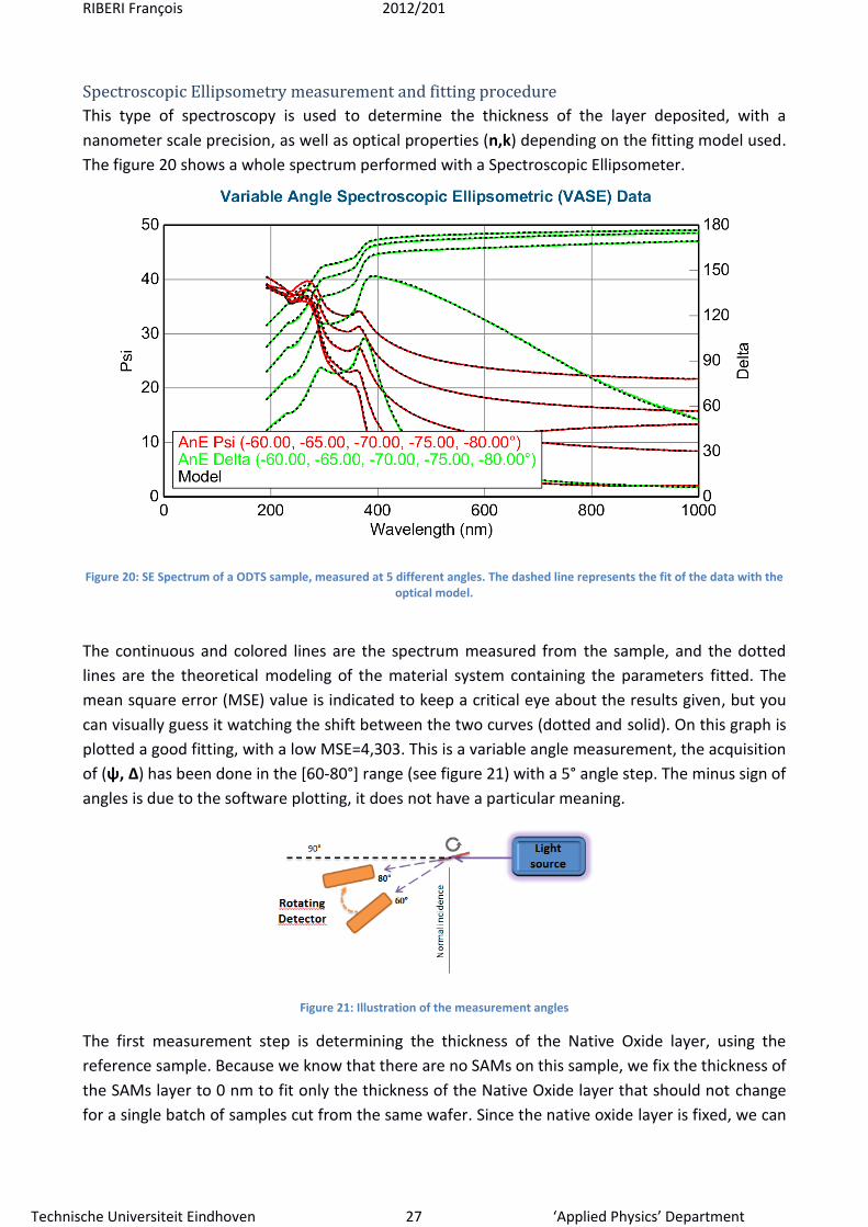
The figure 20 shows a whole spectrum performed with a Spectroscopic Ellipsometer.
Figure 20: SE Spectrum of a ODTS sample, measured at 5 different angles. The dashed line represents the fit of the data with the optical model.
The continuous and colored lines are the spectrum measured from the sample, and the dotted
lines are the theoretical modeling of the material system containing the parameters fitted. The
mean square error (MSE) value is indicated to keep a critical eye about the results given, but you
can visually guess it watching the shift between the two curves (dotted and solid). On this graph is
plotted a good fitting, with a low MSE=4,303. This is a variable angle measurement, the acquisition
of (ψ, Δ) has been done in the [60-80°] range (see figure 21) with a 5° angle step. The minus sign of
angles is due to the software plotting, it does not have a particular meaning.
Figure 21: Illustration of the measurement angles
The first measurement step is determining the thickness of the Native Oxide layer, using the
reference sample. Because we know that there are no SAMs on this sample, we fix the thickness of
the SAMs layer to 0 nm to fit only the thickness of the Native Oxide layer that should not change
for a single batch of samples cut from the same wafer. Since the native oxide layer is fixed, we can
RIBERI François 2012/201
Technische Universiteit Eindhoven 28 ‘Applied Physics’ Department
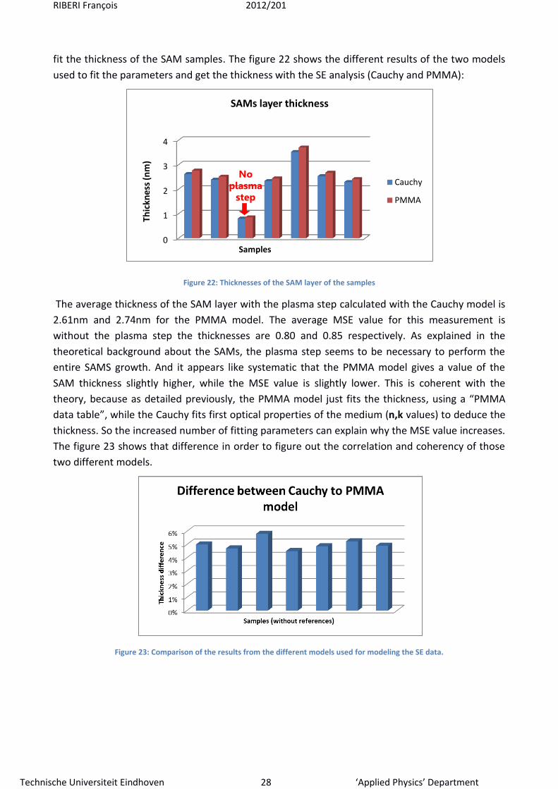
fit the thickness of the SAM samples. The figure 22 shows the different results of the two models
used to fit the parameters and get the thickness with the SE analysis (Cauchy and PMMA):
Figure 22: Thicknesses of the SAM layer of the samples
The average thickness of the SAM layer with the plasma step calculated with the Cauchy model is
2.61nm and 2.74nm for the PMMA model. The average MSE value for this measurement is
without the plasma step the thicknesses are 0.80 and 0.85 respectively. As explained in the
theoretical background about the SAMs, the plasma step seems to be necessary to perform the
entire SAMS growth. And it appears like systematic that the PMMA model gives a value of the
SAM thickness slightly higher, while the MSE value is slightly lower. This is coherent with the
theory, because as detailed previously, the PMMA model just fits the thickness, using a “PMMA
data table”, while the Cauchy fits first optical properties of the medium (n,k values) to deduce the
thickness. So the increased number of fitting parameters can explain why the MSE value increases.
The figure 23 shows that difference in order to figure out the correlation and coherency of those
two different models.
Figure 23: Comparison of the results from the different models used for modeling the SE data.
0
1
2
3
4 Th
ickn
ess
(nm
)
SAMs layer thickness
Cauchy
PMMA
Samples
No plasma
step
RIBERI François 2012/201
Technische Universiteit Eindhoven 29 ‘Applied Physics’ Department
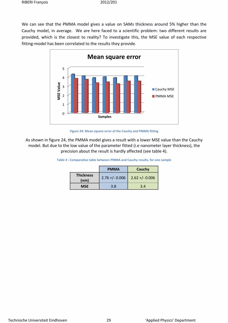
We can see that the PMMA model gives a value on SAMs thickness around 5% higher than the
Cauchy model, in average. We are here faced to a scientific problem: two different results are
provided, which is the closest to reality? To investigate this, the MSE value of each respective
fitting-model has been correlated to the results they provide.
Figure 24: Mean square error of the Cauchy and PMMA fitting
As shown in figure 24, the PMMA model gives a result with a lower MSE value than the Cauchy model. But due to the low value of the parameter fitted (i.e nanometer layer thickness), the
precision about the result is hardly affected (see table 4).
Table 4 : Comparative table between PMMA and Cauchy results, for one sample
PMMA Cauchy
Thickness (nm)
2.76 +/- 0.006 2.62 +/- 0.006
MSE 3.8 3.4
0
1
2
3
4
5
MSE
Val
ue
Samples
Mean square error
Cauchy MSE
PMMA MSE
RIBERI François 2012/201
Technische Universiteit Eindhoven 30 ‘Applied Physics’ Department
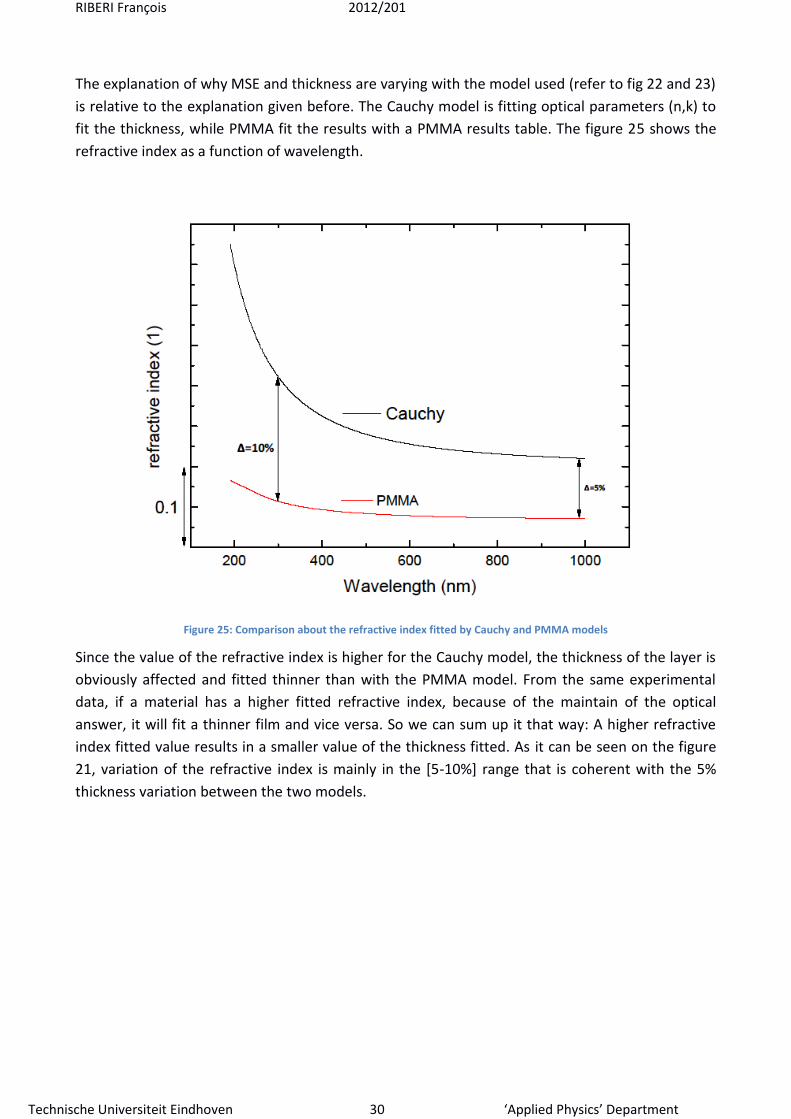
The explanation of why MSE and thickness are varying with the model used (refer to fig 22 and 23)
is relative to the explanation given before. The Cauchy model is fitting optical parameters (n,k) to
fit the thickness, while PMMA fit the results with a PMMA results table. The figure 25 shows the
refractive index as a function of wavelength.
Figure 25: Comparison about the refractive index fitted by Cauchy and PMMA models
Since the value of the refractive index is higher for the Cauchy model, the thickness of the layer is
obviously affected and fitted thinner than with the PMMA model. From the same experimental
data, if a material has a higher fitted refractive index, because of the maintain of the optical
answer, it will fit a thinner film and vice versa. So we can sum up it that way: A higher refractive
index fitted value results in a smaller value of the thickness fitted. As it can be seen on the figure
21, variation of the refractive index is mainly in the [5-10%] range that is coherent with the 5%
thickness variation between the two models.
RIBERI François 2012/201
Technische Universiteit Eindhoven 31 ‘Applied Physics’ Department
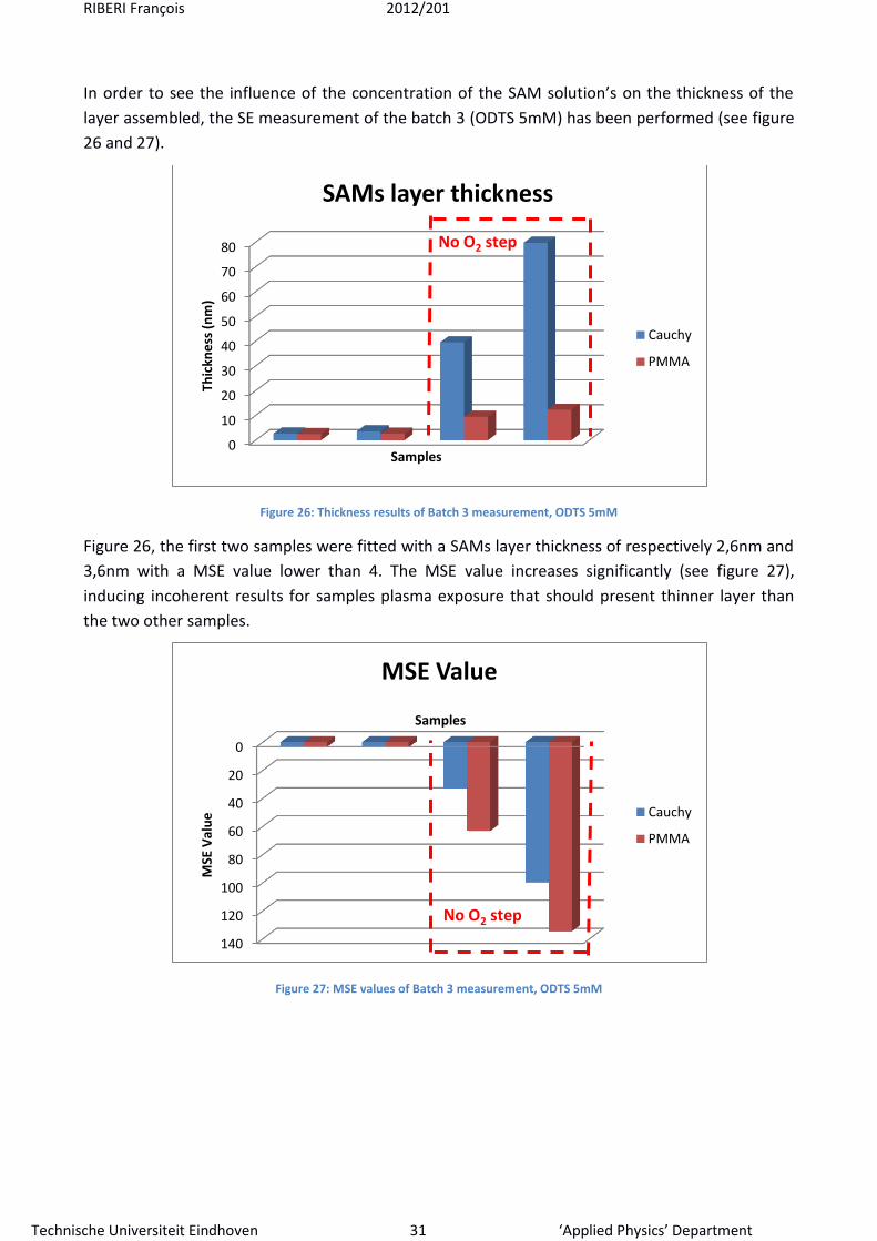
In order to see the influence of the concentration of the SAM solution’s on the thickness of the
layer assembled, the SE measurement of the batch 3 (ODTS 5mM) has been performed (see figure
26 and 27).
Figure 26: Thickness results of Batch 3 measurement, ODTS 5mM
Figure 26, the first two samples were fitted with a SAMs layer thickness of respectively 2,6nm and
3,6nm with a MSE value lower than 4. The MSE value increases significantly (see figure 27),
inducing incoherent results for samples plasma exposure that should present thinner layer than
the two other samples.
Figure 27: MSE values of Batch 3 measurement, ODTS 5mM
0
10
20
30
40
50
60
70
80
Thic
kne
ss (
nm
)
Samples
SAMs layer thickness
Cauchy
PMMA
No O2 step
0
20
40
60
80
100
120
140
MSE
Val
ue
Samples
MSE Value
Cauchy
PMMA
No O2 step
RIBERI François 2012/201
Technische Universiteit Eindhoven 32 ‘Applied Physics’ Department
(3-Aminopropyl)thimethoxysilane (APTMS)
FTIR Absorption Spectroscopy
The FTIR diagnostic is used to prove the presence of SAMs at the sample surface, and to identify
the chemical composition of them. The FTIR spectra show the Absorbance as a function of the
wavenumber in .
Figure 28: FTIR Absorption Spectrum, APTMS C=1mM
The FTIR absorbance spectrum from the APTMS batch is different, see figure 28, due to the other
composition of the SAM. The ATPMS contains a carbon chain but with one N atom at one of his
extremity. Because it is another carbon chain, there are again the C-O stretching (1030 and
1115 ) and the “doublets” (2886 and 2929 ). Between 1275 and
1545 resonances, that are likely to be the C- stretching followed by the NH2 scissoring
(1577 . A really weak broad peak [2117-2172 could be the R-N-C [2110-2175 ]
and the last one, weak and broad, is likely to be N-H [3270-3470 . About the intensity of the
peaks, all the curves except the blue one are as intense, so no conclusion about plasma exposure
can deduced.
RIBERI François 2012/201
Technische Universiteit Eindhoven 33 ‘Applied Physics’ Department
Spectroscopic Ellipsometry
The first measurement was to control the thickness of the layer after a long time immersion time
(144h). The results are shown figure 29 and were fitted with a high MSE value (see figure 30,
mse>20 is the best condition). Since the MSE value is so high, it’s hard to make conclusion about
results.
Figure 29: Results of Batch 2 measurement, APTMS c=1mM
Figure 30: MSE value of Batch 2 measruments, APTMS c=1mM
We decided then to re-measure the APTMS layer thickness but after different immersion time, in
order to calculate the APTMS growth rate. But results were provided with a high MSE value, and
were absolutely incoherent (typically thickness of the SAM layer thinner after 30min immersion
than 20 minutes). An hypothesis reason has been putted forward: the measurement process was
not good, due to the fact that all the samples were located in the same glass beaker. By taking out
a sample, the SAMs solution was disturbed. The next experiment is to re-do the growth rate
measurement, making one stock solution of APTMS in Toluene at a certain concentration, split it in
several space isolated glass beaker, immerse the samples “all the same time” and emerge them
disturbing the beaker or shaking them strongly.
65
70
75
80
85
Thic
kne
ss (
nm
)
Samples
SAMs layer thickness
Cauchy
PMMA
No O2 step
0
20
40
60
80
100
MSE
Val
ue
Samples
MSE Value
Cauchy
PMMA
No O2 step
RIBERI François 2012/201
Technische Universiteit Eindhoven 34 ‘Applied Physics’ Department
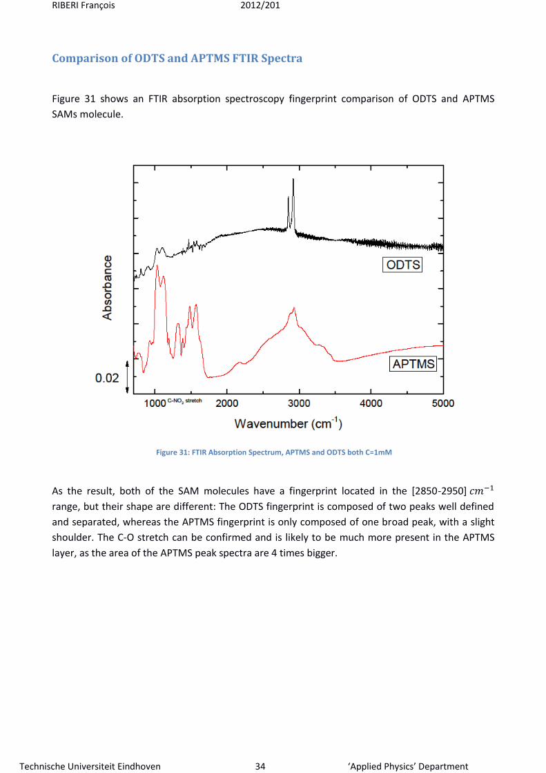
Comparison of ODTS and APTMS FTIR Spectra
Figure 31 shows an FTIR absorption spectroscopy fingerprint comparison of ODTS and APTMS
SAMs molecule.
Figure 31: FTIR Absorption Spectrum, APTMS and ODTS both C=1mM
As the result, both of the SAM molecules have a fingerprint located in the [2850-2950]
range, but their shape are different: The ODTS fingerprint is composed of two peaks well defined
and separated, whereas the APTMS fingerprint is only composed of one broad peak, with a slight
shoulder. The C-O stretch can be confirmed and is likely to be much more present in the APTMS
layer, as the area of the APTMS peak spectra are 4 times bigger.
RIBERI François 2012/201
Technische Universiteit Eindhoven 35 ‘Applied Physics’ Department
V. Conclusion and discussion
Silane-terminated self-assembled monolyer (SAM) film was successfully prepared on
substrate by means of wet chemistry. With FTIR absorption spectroscopy, a fingerprint of (3-
Aminopropyl)thimethoxysilane (APTMS) and Octadecyltrichlorosilane (ODTS) SAM has been
established. The thickness of both APTMS and ODTS films has been investigated with
spectroscopic ellipsometry (SE). For the APTMS it was found that ultra-thin films with variable
thickness (0-100 nm) can be grown. However, the reproducibility of this process is not yet reliable.
The results for the ODTS are indicating that a single layer of SAM is formed and that it is not
possible to growth films of variable thickness. The influence of both the concentration of the SAM
solution and the immersion time on structure and thickness of the SAM was studied. Within the
examined concentration range (1-5 mM), no ??differences?? were found for both ODTS and
APTMS. With respect to immersion time, once ODTS layers were completely developed, exposure
time had no impact on the thickness nor on the structure. On the other hand, for APTMS the
thickness and structure do depend on immersion time. Also, the influence of surface
functionalization with a O2 plasma was investigated. For ODTS, it is found that a higher surface
coverage is achieved with plasma pre-treatment. Due to a lack of trend, no conclusion can be
drawn about plasma pre-treatment influence on the APTMS self-assembling. This absence of a
trend is likely to be caused by a disturbance introduced by sample handling.
Because the thinnest SAMs have a thickness of approximately 2 nm, the sensitivity of the SE
measurement has to be good enough to resolve sub nanometer differences. Therefore, the
characterization of the substrate, i.e. the Si(100) wafer and the native oxide, has to be performed.
In contrast to conventional SE measurements, a reference measurement characterizing the native
oxide layer is crucial in the determination of the SAM thickness. In the modeling of SE data
obtained from the SAM on the Si(100) wafer, both the Cauchy and the PMMA models are valid
and yield a comparable thickness. The Cauchy model always results in a 5% thinner layer, which
can be explained by the fixed, underestimated, refractive index of the PMMA model.
As a continuation of this work, two main topics should be investigated.
Perform growth rate APTMS experiment, taking care that the SAM growth is not disturbed. This can be done by, for example, placing each sample in a single container. Thereby, the sample extraction and handling will not induce any changes during the self-assembly of other samples. This would be an approach to confirm the growth rate established in literature.
Regarding the results with APTMS precursor, a linear time dependence of the thickness was expected from literature. A cause for this absence of this result could be the influence of the depletion of SAM precursor during the growth and self-assembly. To clarify the impact of depletion, an experiment setup could be to grow SAMs using a broad range (e.g. 1-50 mM) of concentrations.
With the SAMs a valuable asset is available for characterizing surface sensitive diagnostic
techniques, such as broadband sum-frequency generation and IR spectroscopic ellipsometry. With
this work it will be possible to reliably grow the samples needed for the BB-SFG of the SAMs.
Furthermore, the interpretation of the linear spectrum will aid the interpretation of the nonlinear
SFG response of the SAMs.
RIBERI François 2012/201
Technische Universiteit Eindhoven 36 ‘Applied Physics’ Department
VI. Bibliography
[1] International Energy Agency. "Energy Technology Perspectives 2012".
[2] European Photovoltaic Industry Association. "Global Market Outlook for Photovoltaics 2013-
2017".
[3] B. Morgan, O. Ijeoma, L. Michael, M. Ian, C. Jennifer, S. Jigar, G. Dolf et al., "Re-considering
the Economics of Photovoltaic Power." 1–19.
[4] K. Ramanathan, M.A. Contreras, C.L. Perkins, S. Asher, F.S. Hasoon, J. Keane, D. Young et
al. (2003). "Properties of 19.2% efficiency ZnO/CdS/CuInGaSe2 thin-film solar cells. Progress in
Photovoltaics: Research and Applications." 11(4), 225–230.
[5] i J. Sterner (2004). "ALD Buffer Layer Growth and Interface Formation on Cu(In ,Ga)Se2
Solar Cell Absorbers."
ii S. M. George (2010). "Atomic layer deposition: an overview." Chemical reviews, 111–31.
[6] G. Dingemans, R. Seguin, P. Engelhart, M. C. M. Van De Sanden, W. M. M. Kessels, (2010).
"Silicon surface passivation by ultrathin Al2O3 films synthesized by thermal and plasma atomic
layer deposition." - Rapid Research Letters, 4(1-2), 10–12.
[7] D. R. G. Mitchell, G. Triani, D. J Attard, K. S. Finnie, P. J. Evans, C. J. Barbé, & J. R. Bartlett,
(2006). "Atomic layer deposition of TiO2 and Al2O3 thin films and nanolaminates." Smart
Materials and Structures. S57–S64.
[8] G. Dingemans, C. A. A.Van Helvoirt, M. C. M. Van De Sanden, W. M. M. Kessels, (2011).
"Plasma-Assisted Atomic Layer Deposition of Low Temperature SiO2." 191–204.
[9] Z. L. Wang, (1998). "Structural Analysis of Self-Assembling Nanocrystal Superlattices."
Advanced Materials.
[10] A. Ulman, (1996). "Formation and Structure of Self-Assembled Monolayers." Chemical
reviews. 1533–1554.
[11] L. He, S. Guang, H. Song, (1999). "Physics of NonLinear Optics."
[12] Robert W. Boyd, (2008). "Nonlinear Optics" (third edition)
[13] H. Fujiwara, (2007). "Spectrosopic Ellipsometry Principles and Applications."
[14] http://teaching.shu.ac.uk/hwb/chemistry/tutorials/molspec/irspec1.htm
C. Berthomieu, & R. Hienerwadel, (2009). "Fourier transform infrared (FTIR) spectroscopy."
Photosynthesis research, 157–70.
[15] Princeton Instrument, "Raman Spectroscopy Basics",1–5.
[16] P. Silberzan, L. Legér, D. Ausserré, J.J. Benattar, (1991), Langmuir, 7, 1647
[17] S.R. Wasserman, Y. –T. Tao, J.M. Whitesides (1989), Langmuir, 5, 1074
[18] R. Banga, J. Yarwood, A.M. Morgan, B. Evans, J. Kells, (1995), Langmuir, 11, 4393
[19] A. K. Chauhan, D.K. Aswal,., S.P. Koiry, S.K. Gupta, J.V.Yakhmi, C. Sürger, D. Guerin
et.al.(2007). "Self-assembly of the 3-aminopropyltrimethoxysilane multilayers on Si and hysteretic
current–voltage characteristics." Applied Physics, 581–589.

RIBERI François 2012/201
Technische Universiteit Eindhoven 37 ‘Applied Physics’ Department
VII. Acknowledgements
First of all I would like to thank the teacher thanks to I could have come here, in Eindhoven, to
perform this project, M. Boufendi Laifa. I want to thank obviously the PMP group from the TU/e
leaded by Prof.dr.ir. Erwin Kessels, and composed of attentive and helpful people. The students took time to
explain me things about university and physics, which was very thoughtful of them. I would like to thank
particularly my supervisor, Mr. Vandalon Vincent (corrector of this report), for having been attentive patient
and generous throughout the entire project. It was a real pleasure to discuss about optic and
physic with a passionate PhD student as him. This passage in the PMP group has been extremely
exciting and formative for me, Thank you to all having been contributing near and far. Thank you
also to Bart Macco for taking the time to share his work to me and his knowledge about in –situ
ellipsometry, and thank you to Cristian van Helvoirt and Bas van de Loo to be made available each
time I needed to perform the plasma process.