Embed Size (px)
Citation preview
Efficiency Enhancement Techniques in Integrated Tri-mode DC-DC Converters
by
Ge Jin
A thesis submitted in conformity with the requirements for the degree of Master of Applied Science
Department of Electrical and Computer Engineering University of Toronto
© Copyright by Ge Jin 2015

ii
Efficiency Enhancement Techniques in Integrated Tri-mode DC-
DC Converters
Ge Jin
Master of Applied Science
Department of Electrical and Computer Engineering
University of Toronto
2015
Abstract
This thesis presents a tri-mode dc-dc converter that can operate in buck, boost and buck-boost
configuration. A power transmission gate is implemented in the converter as the high side driver
of the H-bridge output stage. A one-step dead-time correction technique is also implemented
based on a previous work of buck converter topology. This tri-mode converter is designed to use
the lithium-ion battery as input voltage source (2.7 to 4.2V) and provide an output voltage from 1
to 5V with an output current of up to 0.5A. The switching frequency is fixed at 1.5MHz.
This converter combines different efficiency enhancement techniques such as power
transmission gate, one-step dead-time correction and segmented power devices on one chip
which increases the complexity of integrated circuit implementation. A peak efficiency of 93% is
observed in the boost mode. A further improvement of 3.3% in the peak efficiency is achieved
with dead-time correction.

iii
Acknowledgments
In my way of seeking truth and wisdom, my supervisor, Wai Tung Ng, continually and
convincingly conveyed the spirit of professionalism and perfectionism in both work and life. I
would like to express my sincere gratitude to him for revising my papers in the late nights, for his
profound comments and critiques on my works, for giving me opportunities attending
conferences, for encouraging me to try my ideas and tolerating failures. Without his guidance
and persistent help, this research would not have been possible.
I would like to thank everybody in the group: Jingshu Yu, Andrew Shorten, Jingxuan Chen,
Sherrie Xie, Weijia Zhang, Robert McKenzie, Rophina Li and Mengqi Wang. Without you guys,
work at school would be insipid and unproductive.
Special thanks to Zhihua Ning, from Zhejiang University, China. I really appreciate Zhihua’s
help in academia field. I was therefore encouraged by him to overcome many obstacles in my
studies. I’m also very grateful to Silu Cheng, from Tianjin University, China. Without her
exhaustively help on my project, it would be much harder to finish this thesis.
I would like to extend my deepest gratitude to my fiancée, Qingyi Guan. Without her
encouragement and taking care of me, I wouldn’t push myself to study hard and work her to give
her a promising future.
Last but not least, the many years of support from my parents, Xiaochun Jin and Shujie Song,
was exceptionally appreciated. Their endless love and encouragement facilitated me to finish my
undergraduate and master degrees and set me free to chase my dreams without any worry. Their
dedication gave the foundation of this work.

iv
Table of Contents
Table of Contents ........................................................................................................................... iv
List of Publications ....................................................................................................................... vii
List of Glossary ............................................................................................................................ viii
List of Tables .................................................................................................................................. x
List of Figures ................................................................................................................................ xi
Chapter 1 Introduction ............................................................................................................. 1
1.1 Background of Portable Devices Power Management ....................................................... 1
1.1.1 State-of-the-Art and Comparison of Power Management Circuits ......................... 2
1.1.2 Advantages in Tri-mode dc-dc Converter ............................................................... 4
1.2 Research Objectives ............................................................................................................ 5
1.3 Thesis Organization ............................................................................................................ 5
Chapter 2 Fundamentals of Tri-mode dc-dc Converters ......................................................... 7
2.1 Buck-boost Converters ........................................................................................................ 7
2.2 Basics of Non-inverting Buck-boost Converters ................................................................ 9
2.3 Tri-mode dc-dc Converters ............................................................................................... 10
2.3.1 Operation Mode Selection of the Tri-mode Converter ......................................... 12
2.4 Sources of Power Losses in Tri-mode Converters ............................................................ 13
2.4.1 Conduction Loss ................................................................................................... 13
2.4.2 Body-diode Loss ................................................................................................... 14
2.4.3 Switching Loss ...................................................................................................... 15
2.4.4 Gate-Drive Loss .................................................................................................... 16
2.4.5 Passive Component Losses ................................................................................... 16
2.5 Summary ........................................................................................................................... 17
Chapter 3 Efficiency Enhancement Techniques .................................................................... 18

v
3.1 Design Overview of an Integrated Tri-mode Converter ................................................... 18
3.2 Power Transmission Gate ................................................................................................. 20
3.2.1 Background and Introduction of Power Transmission Gate ................................. 20
3.2.2 Working Principle of Power Transmission the Gate ............................................ 23
3.2.3 Simulation Result and Discussion ........................................................................ 24
3.3 One-step Dead-time correction ......................................................................................... 26
3.3.1 Background and Introduction of Dead-time Correction ....................................... 27
3.3.2 Working Principle of Dead-time Correction ......................................................... 28
3.4 Segmented Power Device Structure .................................................................................. 31
3.5 Summary ........................................................................................................................... 34
Chapter 4 IC Implementation and Experimental Results ...................................................... 35
4.1 IC Implementation ............................................................................................................ 35
4.1.1 Metallization Optimization of the Power Devices ................................................ 37
4.1.2 R3D Simulation for the Top Metal Layer of the Power Devices ......................... 40
4.2 Printed Circuit Board (PCB) Implementation ................................................................... 43
4.2.1 Circuit Board for Power Conversion Efficiency Test ........................................... 43
4.2.2 Test Board with One-Step Dead-time correction Circuit ..................................... 44
4.3 Tri-mode Operation .......................................................................................................... 45
4.4 Efficiency Measurements .................................................................................................. 47
4.4.1 Efficiency Improvement with Power Transmission Gate ..................................... 47
4.4.2 Efficiency Improvement with One-Step Dead-time correction ............................ 50
4.4.3 Efficiency Improvement with Segmented Power Devices ................................... 54
4.5 Summary ........................................................................................................................... 57
Chapter 5 Conclusion and Future Tasks ................................................................................ 58
5.1 Thesis Summary and Contributions .................................................................................. 58
5.2 Future Work ...................................................................................................................... 60

vi
References ..................................................................................................................................... 61
Copyright Acknowledgements ...................................................................................................... 65

vii
List of Publications
1) G. Jin, W.T. Ng, “An Integrated Tri-mode Non-inverting Buck-Boost dc-dc Converter with
Segmented Power Devices and Power Transmission Gate Structure,” in International
Symposium on Power Semiconductor Devices and IC's (ISPSD 2014), Waikoloa, Hi, Jun. 15-
19, pp. 201-204, 2014.
2) Z. Ning, L. He, Z. Hu, G. Jin, W.T. Ng, “A feedback-voltage-sensing translator for floating
buck dc-dc converters”, 2013 IEEE International Conference of Electron Devices and Solid-
State Circuits (EDSSC 2013), Jun. 3-5, 2013.
3) S. Cheng, S. Yao, G. Jin, W.T. Ng, “Digital Controlled Dead-time for Tri-mode Buck-boost
dc-dc Converters”, 2014 IEEE 12th
International Conference on Solid-State and Integrated
Circuit Technology (ICSICT 2014), Guilin, China, pp. 1580-1582, Oct. 28-31, 2014.

viii
List of Glossary
Vin Input Voltage
Vout Output Voltage
Iout Output Current
Vth Threshold Voltage
Vdd Supply Voltage
CGD Gate to Drain Capacitance
CGS Gate to Source Capacitance
CDS Drain to Source Capacitance
Ciss Input Capacitance
Coss Output Capacitance
Crss Reverse Transfer Capacitance
D Duty Ratio
fsw Switching Frequency
IDS Drain to Source Current
IG Gate Current
M Conversion Ratio
η Efficiency
Ploss Total Power Loss
Pcond Conduction Power Loss

ix
Pgate Gate Drive Power Loss
Psw Switching Power Loss
Pbd Body-diode Power Loss
Prr Reverse Recovery Loss
Pco Output Capacitor Loss
Pind Inductor Loss
QG Gate Charge
Qrr Reverse Recovery Charge
Ron On-resistance (of Power MOSFETs)
Ron,sp Specific On-resistance
τoff Turn-off Time
τon Turn-on Time
Ts Switching Period
VDS Drain to Source Voltage
VGS Gate to Source Voltage
Vgate Gate Voltage
W Gate Width

x
List of Tables
Table 1-1 COMPARISON of THREE TYPES OF VOLTAGE REGULATORS ......................... 3
Table 2-1 POWER DEVICES STATUS OF TRI-MODE dc-dc CONVERTERS ...................... 11
Table 3-1 OPERATION CONDITION OF HS2_P AND HS2_N IN THE POWER
TRANSMISSION GATE ............................................................................................................. 24
Table 4-1 ON-STATE RESISTANCE OF EACH SEGMENT FOR THE POWER DEVICES . 42
Table 4-2 SUMMARY OF CONVERTER IC AND EXPERIMENTAL RESULTS .................. 57
Table 5-1 COMPARISON TABLE WITH OTHER WORKS ..................................................... 59

xi
List of Figures
Figure 1-1 General power management solution in portable applications. .................................... 1
Figure 2-1 Buck-boost converter topology. .................................................................................... 7
Figure 2-2 Synchronous inverting buck-boost converter topology. ............................................... 8
Figure 2-3 Non-inverting buck-boost dc-dc converter topology. ................................................... 9
Figure 2-4 Switching signals for the four switches in a non-inverting buck-boost dc-dc converters.
....................................................................................................................................................... 10
Figure 2-5 Operating status of the MOSFETs in buck mode, buck-boost mode and boost mode
and their gate control signals. ....................................................................................................... 11
Figure 2-6 Four-switch tri-mode converter topology with sources of power lesses labelled. ...... 13
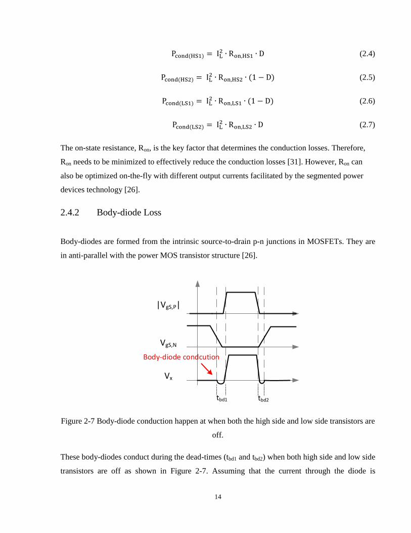
Figure 2-7 Body-diode conduction happen at when both the high side and low side transistors are
off. ................................................................................................................................................. 14
Figure 2-8 Hard switching waveform with switching losses and conduction loss labelled. ........ 15
Figure 3-1 Circuit topology of a traditional non-inverting buck-boost dc-dc converter. ............. 18
Figure 3-2 The proposed tri-mode dc-dc converter with a power transmission gate as the HS2
driver. ............................................................................................................................................ 19
Figure 3-3 Power transmission gate used as the high side driver, HS2. ....................................... 20
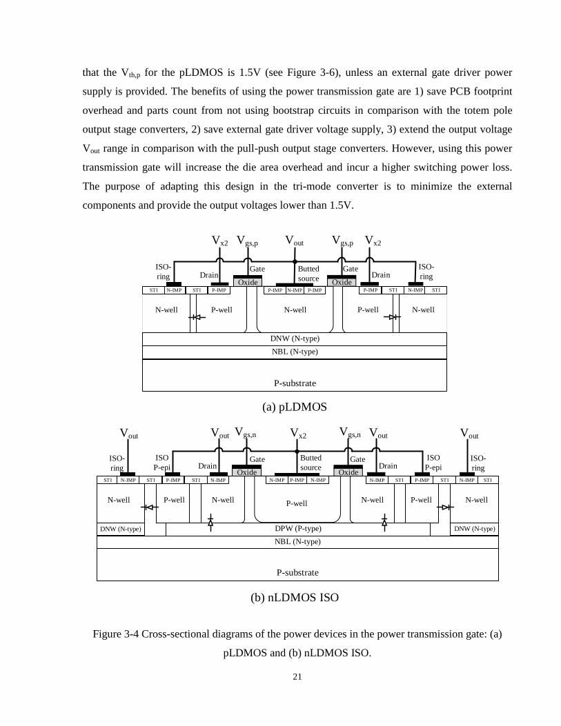
Figure 3-4 Cross-sectional diagrams of the power devices in the power transmission gate: (a)
pLDMOS and (b) nLDMOS ISO. ................................................................................................. 21
Figure 3-5 Cross-sectional diagram of the guard ring for the power devices. .............................. 22
Figure 3-6 On-state resistance diagram and the operation ranges of the transistors in the power
transmission gate. .......................................................................................................................... 23

xii
Figure 3-7 On-state operation areas of power transmission gate. ................................................. 25
Figure 3-8 Efficiency versus Vout/Vin in three modes with and without power transmission gate
enabled. ......................................................................................................................................... 25
Figure 3-9 Switching diagrams for NOR gate body-diode conduction detection circuit: (a) dead-
time too short (b) proper dead-time (c) dead-time too long. ......................................................... 26
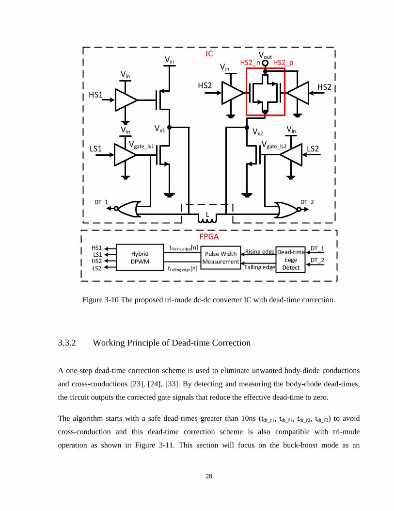
Figure 3-10 The proposed tri-mode dc-dc converter IC with dead-time correction. .................... 28
Figure 3-11 DPWM outputs for the tri-mode converter in buck mode, buck-boost mode and
boost mode. ................................................................................................................................... 29
Figure 3-12 Timing diagram of the edge detection, (a) rising edge and falling edge both need
correction, (b) rising edge needs correction, (c) falling edge needs correction. ........................... 30
Figure 3-13 efficiency vs output currentcurves for increasing power-stage transistor segments. 31
Figure 3-14 The efficiency 3D plot with repect to output current and the size of power transistors.
....................................................................................................................................................... 32
Figure 3-15 The power conversion efficiency versus Iout for different number of power device
segments. ....................................................................................................................................... 33
Figure 4-1 Layout of the tri-mode dc-dc converter with the power transmission gate highlighted.
....................................................................................................................................................... 35
Figure 4-2 The tri-mode converter IC packaged in a 36-pin QFN package. ................................ 36
Figure 4-3 Wire bonding diagram of the tri-mode converter IC. ................................................. 36
Figure 4-4 Top metal layer layout with the power devices labelled in white boxes. ................... 37
Figure 4-5 The power devices used in the tri-mode converter are partitioned into 8 identical
segments. ....................................................................................................................................... 38
Figure 4-6 Two types of current flow happening on the power devices metal layers. ................. 38

xiii
Figure 4-7 Metallization layout styles of the top metal layer. ...................................................... 39
Figure 4-8 On-state resistance of three layout styles with horizontal current flows..................... 40
Figure 4-9 On-state resistance of three layout styles with vertical current flows. ........................ 41
Figure 4-10 Metallization layout for the proposed design. ........................................................... 42
Figure 4-11 PCB for power conversion efficiency test. ............................................................... 43
Figure 4-12 PCB for power conversion efficiency test with one-step dead-time correction circuit.
....................................................................................................................................................... 44
Figure 4-13 Power conversion efficiency of the tri-mode converter operating in three modes with
various input voltages. .................................................................................................................. 45
Figure 4-14 Transitioning from buck mode to buck-boost mode. ................................................ 46
Figure 4-15 Transitioning from buck-boost mode to boost mode. ............................................... 46
Figure 4-16 Power conversion efficiency measured with and without PTG in buck mode. ........ 47
Figure 4-17 Power conversion efficiency measured in buck-boost mode with and without PTG
enabled. ......................................................................................................................................... 48
Figure 4-18 Power conversion efficiency measured in boost mode with and without PTG enabled.
....................................................................................................................................................... 49
Figure 4-19 Timing diagram of the PWM signals and the NOR gate outputs (DT_1 and DT_2) in
different modes. ............................................................................................................................ 50
Figure 4-20 The NOR gate conduction waveforms show that body-diode conductions are
detected. ........................................................................................................................................ 51
Figure 4-21 Power conversion efficiency comparison with and without dead-time correction in
buck-boost mode. .......................................................................................................................... 52

xiv
Figure 4-22 Power conversion efficiency comparison with and without dead-time correction in
boost mode. ................................................................................................................................... 52
Figure 4-23 Power conversion efficiency comparison with and without dead-time correction in
buck mode. .................................................................................................................................... 53
Figure 4-24 Measured power efficiency using segmented output in buck mode. ........................ 54
Figure 4-25 Power conversion efficiency with segmented output stage in buck-boost mode. ..... 55
Figure 4-26 Power conversion efficiency with segmented output stage in boost mode. .............. 55

1
Chapter 1 Introduction
This chapter introduces the basic ideas and motivation of this thesis. The current solutions for
power management in modern portable devices are discussed. With an in-depth comparison of
these solutions, the reason for selecting the tri-mode dc-dc converter is explained. Finally, the
thesis organization is provided.
1.1 Background of Portable Devices Power Management
With the dramatically increasing demand of power drawn from the batteries with limited size and
weight, the portable electronics industry is confronting the trade-off between functionality,
performance and battery life. In order to extend the battery life of portable devices and adapting
large LCD screens and powerful CPUs, etc., designers could make their products greater in size
or could use a more efficient power management solution in their products [1]. However, making
things bigger is not an option as it goes against the trend of modern portable devices designs
especially in wearable applications. The motivation of the thesis is to find a better solution to
enhance the power conversion efficiency in portable devices.
Lithium-ion battery
Charger System Control and monitoring
LDO
Front-end dc-dc converter
Battery Management Multiple Output Voltages
Lithium-ion Battery
Intermediate bus
DC Inputs
SMPS
LDO
SMPS
Loads
.
.
.
.
.
.
Figure 1-1 General power management solution in portable applications.

2
Portable handheld computing devices are typically wireless, light-weight and commonly with a
touch sensitive LCD display. Smartphones, wearable devices, PDAs, music players, etc. are the
most common portable devices. Figure 1-1 shows a general power management solution for
portable applications [2]. Basically, there are two major parts in a portable devices power
management system: battery management and multiple output voltage regulators (LDO, SMPS,
etc.). The battery management includes the battery charging control, battery monitoring and
front-end dc-dc converter. It also provides information on the charging status, battery
authenticity and battery life remaining to the operating system. This allows the operating system
to activate battery saving mode in certain situations to extend the battery life. Actually, for
certain power consumption, the battery life is determined by the battery capacity and power
conversion efficiency of the voltage regulators. This thesis focuses on the power conversion
efficiency enhancement for the front-end dc-dc converter only. The comparison between
different converter circuits and the motivation of choosing the tri-mode dc-dc converter
(highlighted in red in Figure 1-1) for implementation is also provided in later sections.
1.1.1 State-of-the-Art and Comparison of Power Management Circuits
There are three major types of voltage regulators: low drop-out voltage regulator (LDO),
switched capacitor dc-dc (SC converter) converter and switched-mode power supply (SMPS).
Table 1-1 compares the most important properties of these converters (next page).
According to Table 1-1, SMPS stands out as an ideal choice for high power conversion
efficiency despite its size and cost disadvantages. If PCB space, small size and low cost are the
limitations, SMPS would not be a good choice [3]. Since an inductor has to be used as a critical
component in SMPS, miniaturizing the SMPS converter is quite challenging. However,
engineers keep pushing the switching frequency to 100’s MHz range to reduce the inductive
component’s size in modern applications.

3
Table 1-1 COMPARISON of THREE TYPES OF VOLTAGE REGULATORS
Property LDO SC converter SMPS
Efficiency [4], [5] Low Medium High
Size (mm3/
W) [5] Low Medium High
Cost ($/W) [5] Low Medium High
Noise [4], [6] Low Medium High
Step-up Voltage No Yes Yes
Output current [4], [7] Medium Low High
Magnetic component No need No need Needed
Footprint [4], [5], [8], [9] Small Medium Medium
The LDO is often used for low power consuming devices. For example, Nike+ FuelBand [10]
and Motorola Moto 360 [11] use LDO ICs from Texas Instruments, TPS78218 and TPS659120,
respectively as their power management solutions. LDOs have many advantages over the SMPS
[4]. They are more suitable for the following applications: 1) simple/low cost solutions, 2) low
noise/low ripple applications, 3) fast transient applications, and 4) low drop applications (where
output voltage is close to the input voltage). However, the major limitations of the LDOs are the
followings: 1) no step-up conversion ability, and 2) conversion efficiency is quite low in high
power high current situation. Therefore, if the trend of the future wearable device is going to
have a larger LCD screen, better graphical processor and CPU, LDO won’t be a good choice.
The main reasons for designers to use SMPSs instead of linear regulators or LDOs are higher
efficiency and higher power density (small size) in high current applications. Examples such as
the Oculus Rift Development Kit 2 [12], Samsung Gear Live [13], LG G Watch [14], Samsung
Gear Fit [15] and Samsung Gear 2 [16] are using SMPS as their power management solutions.
The SC converter or charge pump is somewhere in between. The SC converter has traditionally
been used in low power (<10mW) and low conversion ratio (<4:1) applications where neither
regulation nor efficiency is critical [6]. This type of dc-dc converter is considered as an
alternative to the LDO. However, it has an inherent power loss deficiency when the SC converter
operates between or outside its output target voltages [7]. Moreover, the SC converter exhibits

4
significant efficiency degradation with the varying input voltage [17]. This converter is not a
good alternative to the SMPS especially when the high output current is required.
Since the conversion efficiency is a priority in portable devices, SMPSs are the most commonly
used power converter modules in these devices.
1.1.2 Advantages in Tri-mode dc-dc Converter
The thesis proposes a tri-mode dc-dc converter IC as the solution to overcome the challenges of
portable devices. After comparing the SMPS over other solutions, this section discusses why the
tri-mode converter topology stands out of the buck and boost topologies.
Loads in portable devices such as logic processors, LCD displays, LED lights, mic/speakers,
flash memories, power amplifiers of RF transmitters, require different supply voltages [18], [19].
In general, loads need supply voltages from 1V (logic core), 3.3V (LVTTL) to 5V (TTL) [20],
[21] while the converters take the battery input from 2.7V to 4.2V (nominal voltage is 3.7V) [22].
To meet these requirements, the tri-mode dc-dc converter is an ideal candidate to supply the
voltages beyond and below the input voltage.
Additionally, as a matter of fact that a lithium-ion battery’s supply voltage is gradually dropping
from 3.7V to 2.7V in most cases while discharging, the proposed tri-mode converter is able to
keep extracting the battery power until it’s depleted. For example, during the extracting process,
assuming the target Vout = 3.3V, the converter operates at buck mode while the battery is fully
charged (Vbatt = 4.2V). As the discharging proceeds, the converter switches to buck-boost mode
as the Vbatt comes closer to Vout. Eventually, the converter switches to boost mode as the Vbatt
approaches to its minimum (Vbatt =2.7V). With the fact that the buck mode and boost mode
conversion efficiencies are higher than ones in the buck-boost mode except only if Vout is in the
vicinity of Vbatt. This tri-mode design guarantees that the converter is operating in its most
efficiency favorable modes. On the other hand, the buck or boost converters are not able to do
this: buck converters would stop working when Vbatt drops below the designated voltage and
boost converters couldn’t provide the outputs below the Vbatt.
5
1.2 Research Objectives
The objective of this research is to design a tri-mode dc-dc converter IC implemented with three
efficiency enhancement techniques. The key research contributions which address these goals are
highlighted below:
Development of a power transmission gate on power devices. Adapting this structure
eliminates the necessities of peripheral circuits such as boot-strap circuits or external
gate driver supplies.
An improved one-step dead-time correction [23] is demonstrated. This dead-time
correction method is implemented in an integrated H-bridge output stage for the first
time. This dead-time correction is able to eliminate the body-diode conductions on
the fly while preventing the cross-conductions. The control algorithm is implemented
in an Altera Cyclone IV FPGA by a visiting scholar, Silu Cheng [24].
The converter IC combines different existing efficiency enhancement techniques
including tri-mode operation [25] and segmented power devices [26] in one chip.
The converter is able to running in tri-mode: buck, boost and buck-boost mode. By
switching between these modes, the converter is able to extract the battery from its
fully charged condition (Vbatt = 4.2V) to nearly depleted condition (Vbatt = 2.7V).
Segmented power devices are implemented in the converter IC in order to optimize
the power efficiency over various output currents. In addition, a top metal layer
optimization method is also demonstrated.
1.3 Thesis Organization
This thesis consists of five chapters. Chapter 1 general provides the background information of
the modern power management solutions in portable electronics and points out the motivation
and objectives of this thesis. After reasoning why the tri-mode dc-dc converter is selected to be
implemented in Chapter 1, the fundamentals of this power converter is discussed in Chapter 2. In
Chapter 3, efficiency enhancement techniques including power transmission gate, one-step dead-
time correction and segmented power device structure are explained and discussed. Chapter 4

6
talks about the implementation of the silicon in detail with experimental results provided. Finally,
conclusions and future tasks are provided in Chapter 5.
7
Chapter 2 Fundamentals of Tri-mode dc-dc
Converters
This chapter discusses the basics of buck-boost dc-dc converter and its variants, the non-
inverting buck-boost converter and the tri-mode converter. The tri-mode operation based on the
non-inverting buck-boost converter topology is introduced and explained in Section 2.4. A
detailed analysis of sources of power losses in this converter is also provided.
2.1 Buck-boost Converters
The buck-boost is a popular non-isolated, inverting power stage topology (See Figure 2-1),
sometimes called a step-down/up power stage. Power supply designers choose the buck-boost
converters because the output voltage is inverted from the input voltage, and the output voltage
can be either lower or higher than the input voltage [9], [27].
L C Rload
M
Vin IL
-
+
Diode
Figure 2-1 Buck-boost converter topology.
This topology gets its name from producing an output voltage that can be lower (like a buck
power stage) or higher (like a boost power stage) in magnitude than the input voltage. Also, this
topology is actually derived from combining the buck converter and the boost converter [9].
However, the output voltage is in opposite polarity from the input voltage. The input current for
8
a buck-boost converter is discontinuous or pulsating due to the power switch (M in Figure 2-1)
current that pulses from zero to IL during every switching cycle.
Equation (2.1) provides the conversion ratio relates to the duty ratio (D) in ideal case. The duty
ratio is the percentage of the on-time of the transistor (M) ranging from 0 to 1. The conversion
ratio can range from 0 to in this case.
M(D)
(2.1)
The output current for a buck-boost converter is also discontinuous or pulsating. This is because
the output diode only conducts during a portion of the switching cycle. The output capacitor
supplies the entire load current for the rest of the switching cycle.
Figure 2-2 shows the synchronous version of the converter topology where the power rectifier is
replaced by a power MOSFET (M2).
L C Rload
M1Vin IL
-
+
M2
Figure 2-2 Synchronous inverting buck-boost converter topology.
This synchronous topology increases the power conversion efficiency since the forward voltage
drop of the power MOSFET (M2) is smaller than that of the diode [9], [28]. However, cross
conductions may happen when using the synchronous topology. The high side transistor, M1 and
low side transistor M2 may be turned-on simultaneously, causing a momentary short between the
power supply and ground. This leads to extra switching power loss. Therefore, dead-time
correction technology must be employed to prevent the cross conductions [27]. In this thesis, a
one-step dead-time correction technique will be explained in Section 3.3.
9
This type of converter is also known as inverting buck-boost dc-dc converter because it not only
converts the input voltage level but also inverts it. Due to its inverting property, these circuitries
are not popular for VLSI implementation. In fact, most of the buck-boost power ICs use a non-
inverting configuration as shown in Figure 2-3. A full discussion of this converter topology is
provided in the next section.
2.2 Basics of Non-inverting Buck-boost Converters
Vin
M1
M2
LM3
M4
C Rload
+
Vout
−
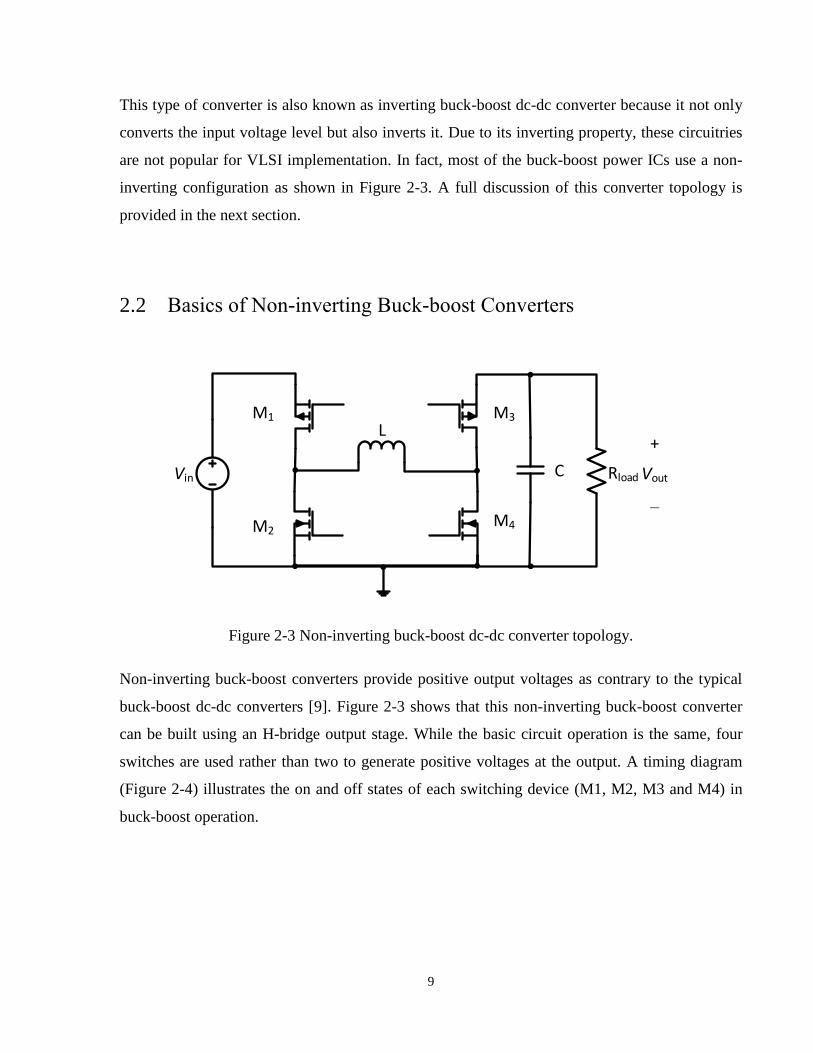
Figure 2-3 Non-inverting buck-boost dc-dc converter topology.
Non-inverting buck-boost converters provide positive output voltages as contrary to the typical
buck-boost dc-dc converters [9]. Figure 2-3 shows that this non-inverting buck-boost converter
can be built using an H-bridge output stage. While the basic circuit operation is the same, four
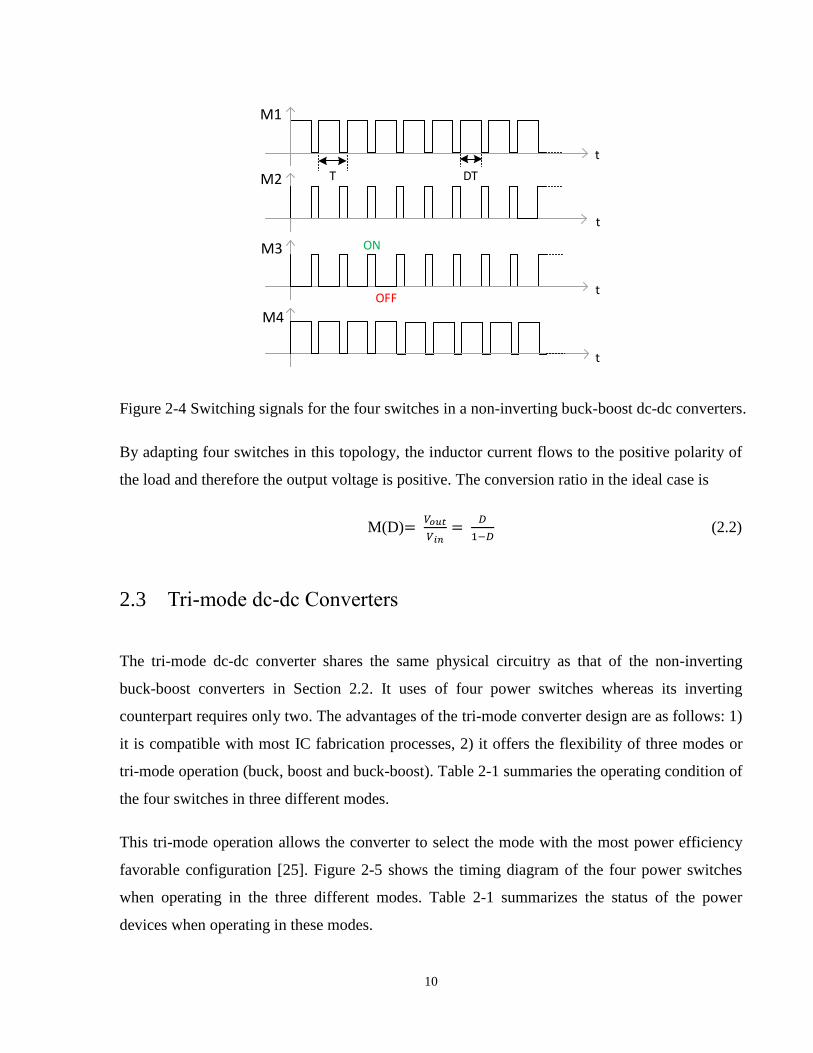
switches are used rather than two to generate positive voltages at the output. A timing diagram
(Figure 2-4) illustrates the on and off states of each switching device (M1, M2, M3 and M4) in
buck-boost operation.
10
M4
M3
M2
M1
DT
t
t
t
t
T
ON
OFF
Figure 2-4 Switching signals for the four switches in a non-inverting buck-boost dc-dc converters.
By adapting four switches in this topology, the inductor current flows to the positive polarity of
the load and therefore the output voltage is positive. The conversion ratio in the ideal case is
M(D)
(2.2)
2.3 Tri-mode dc-dc Converters
The tri-mode dc-dc converter shares the same physical circuitry as that of the non-inverting
buck-boost converters in Section 2.2. It uses of four power switches whereas its inverting
counterpart requires only two. The advantages of the tri-mode converter design are as follows: 1)
it is compatible with most IC fabrication processes, 2) it offers the flexibility of three modes or
tri-mode operation (buck, boost and buck-boost). Table 2-1 summaries the operating condition of
the four switches in three different modes.
This tri-mode operation allows the converter to select the mode with the most power efficiency
favorable configuration [25]. Figure 2-5 shows the timing diagram of the four power switches
when operating in the three different modes. Table 2-1 summarizes the status of the power
devices when operating in these modes.
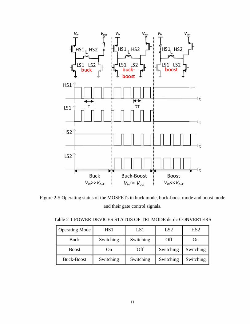
11
LHS1
buck-boost
L HS2
LS1 LS2buck-boost
BuckVin>>Vout
Buck-Boost
Vin Vout
BoostVin<<Vout
LS2
HS2
LS1
HS1
DT
t
t
t
t
T
LHS1 L HS2
LS1 LS2buck
LHS1
boost
L HS2
LS1 LS2
Vin Vout Vin Vout Vin Vout
Figure 2-5 Operating status of the MOSFETs in buck mode, buck-boost mode and boost mode
and their gate control signals.
Table 2-1 POWER DEVICES STATUS OF TRI-MODE dc-dc CONVERTERS
Operating Mode HS1 LS1 LS2 HS2
Buck Switching Switching Off On
Boost On Off Switching Switching
Buck-Boost Switching Switching Switching Switching

12
2.3.1 Operation Mode Selection of the Tri-mode Converter
This section discusses the determining factors of the operation mode selection [25], [29], [30].
The power losses equations can be found in the Section 2.4.
Notice that when operating in buck-boost mode, four power devices are switching continuously
such that the switching loss (Psw) could be twice of that in buck and boost modes. However, in
buck and boost modes, only two devices are switching while the other two are in conduction
mode (turn-on) and turn-off mode. According to (2.3) thru (2.6), conduction loss (Pcond(HS1) in
boost mode or Pcond(HS2) in buck mode) for the inactive transistors would dominate a relatively
large portion of the total power loss. Therefore, the boundaries between buck and buck-boost
modes as well as between the buck-boost and boost modes are located at the balance points
between conduction loss and switching loss [30].
In both buck and boost modes, when Vin = Vout, power transistors HS1 and HS2 are conducting
all the time. Due to the fact that the conduction loss is proportional to the square of IL as
indicated by equation (2.3) and (2.4), the conduction losses from these devices become
significant. Therefore, the converter should operate in buck-boost mode wherever Vout is in the
vicinity of Vin.
On the other hand, according to (2.9), Psw is independent to the duty cycle, D. As Vout deviates
from Vin, the switching loss starts to dominate the total power loss and the converter would
eventually exit from the buck-boost mode where the total Pcond is smaller than or equal to the
total Psw. In conclusion, when Vin >> Vout or Vin << Vout, buck mode and boost mode are more
favorable since they exhibit lower switching and conduction losses [30].
13
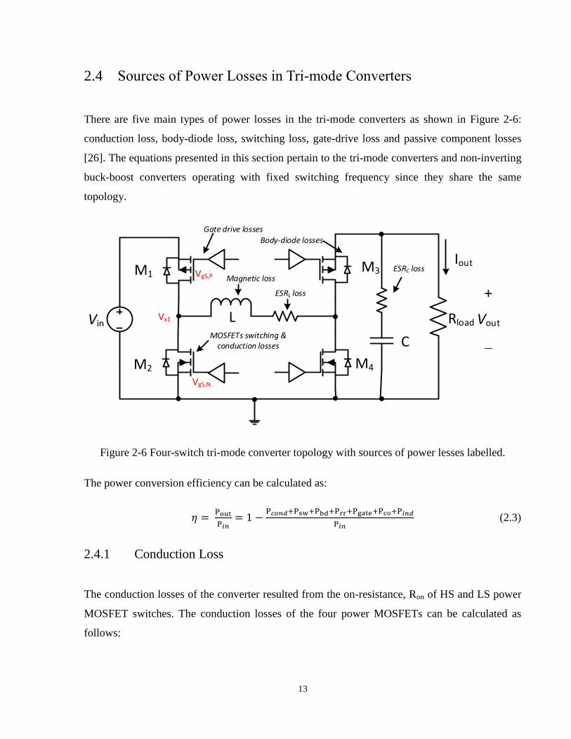
2.4 Sources of Power Losses in Tri-mode Converters
There are five main types of power losses in the tri-mode converters as shown in Figure 2-6:
conduction loss, body-diode loss, switching loss, gate-drive loss and passive component losses
[26]. The equations presented in this section pertain to the tri-mode converters and non-inverting
buck-boost converters operating with fixed switching frequency since they share the same
topology.
Vin
M1
M2
L
M3
M4
C
Rload
+
Vout
Iout
Gate drive losses
MOSFETs switching & conduction losses
Magnetic loss
ESRL loss
ESRC loss
Body-diode losses
VgS,N
VgS,P
Vx1
Figure 2-6 Four-switch tri-mode converter topology with sources of power lesses labelled.
The power conversion efficiency can be calculated as:
(2.3)
2.4.1 Conduction Loss
The conduction losses of the converter resulted from the on-resistance, Ron of HS and LS power
MOSFET switches. The conduction losses of the four power MOSFETs can be calculated as
follows:
14
(2.4)
(2.5)
(2.6)
(2.7)
The on-state resistance, Ron, is the key factor that determines the conduction losses. Therefore,
Ron needs to be minimized to effectively reduce the conduction losses [31]. However, Ron can
also be optimized on-the-fly with different output currents facilitated by the segmented power
devices technology [26].
2.4.2 Body-diode Loss
Body-diodes are formed from the intrinsic source-to-drain p-n junctions in MOSFETs. They are
in anti-parallel with the power MOS transistor structure [26].
Body-diode condcution
Vx
VgS,N
|VgS,P|
tbd1 tbd2
Figure 2-7 Body-diode conduction happen at when both the high side and low side transistors are
off.
These body-diodes conduct during the dead-times (tbd1 and tbd2) when both high side and low side
transistors are off as shown in Figure 2-7. Assuming that the current through the diode is

15
approximately constant when conducting, the body-diode conduction losses Pbd can be
approximated by:
(2.8)
where Vbd is the on-state voltage of the body-diodes. In addition to Pbd, the reverse recoveries
during turn-off also contribute to the total body-diode losses:
(2.9)
where Qrr,N and Qrr,P are the reverse recovery charges for n-channel (LS) body-diode and p-
channel (HS) body-diode, respectively.
2.4.3 Switching Loss
Since size is a big factor in portable devices, reducing the package size or increasing the power
density of dc-dc converter package usually require higher switching frequency [26]. Inevitably,
this leads to higher switching losses.
Switching Losses
IDS
Psw
VDS
τON τOFF
Conduction Loss
Figure 2-8 Hard switching waveform with switching losses and conduction loss labelled.
During the turning on or off of the transistors, none of the voltage across drain and source (VDS)
or the current passing through the transistors (IDS) is equal to zero, this results in power losses
16
(see Figure 2-8) which are directly proportional to the switching frequency, fsw. This type of
power loss is known as switching loss.
The switching loss is proportional to the VDS, IDS, τON and τOFF. The equation is given by:
(2.10)
2.4.4 Gate-Drive Loss
The gate-drive loss is generated from the charging and discharging of input capacitance (Ciss)
when the MOSFET switches at every switching cycle. The gate-drive loss (Pgate) is modeled as:
(2.11)
where QG,HS and QG,LS are the transistor gate charges.
2.4.5 Passive Component Losses
The main motivation for increasing the switching frequency is to reduce the physical size of the
inductor and the output capacitor. For a fixed capacitance, reducing the physical size usually
results in a deterioration of the capacitor equivalent series resistance (ESRc). ESR is derived
from the real component of the capacitor’s impedance at a given frequency. The losses in the
output capacitor and inductor are given by (2.12) and (2.13), respectively.
(2.12)
(2.13)
where RL,dc and RL,ac are the DC and AC equivalent series resistance of the inductor. Actually,
the ESR of the inductor is the major factor that deteriorates the power efficiency and the ESR of
the output capacitor is the major cause of the output voltage ripples.

17
2.5 Summary
This chapter briefly discusses the operating mechanisms of the buck-boost dc-dc converter and
its variants, non-inverting buck-boost dc-dc converter and tri-mode dc-dc converter. A tri-mode
topology with a four-switch H-Bridge output stage is introduced and explained. The significance
of the tri-mode converter is the ability to operate in the most power efficient mode. Moreover,
this chapter provides a comprehensive understanding on the sources of power losses in the tri-
mode dc-dc converters.
18
Chapter 3 Efficiency Enhancement Techniques
Power conversion efficiency is the key parameter that values power converters. Engineers have
been investigating techniques in all aspects to improve the efficiency. This chapter describes the
efficiency improving techniques such as one-step dead-time correction (Section 3.3) and
segmented devices (Section 3.4). A power transmission gate design for the output power stage
(Section 3.2) is also discussed.
3.1 Design Overview of an Integrated Tri-mode Converter
Battery life in portable devices is one of the most critical specifications especially in portable
electronic. This chapter presents efficiency improvement techniques implemented in a 1.5 MHz
tri-mode dc-dc converter using Dongbu HiTek’s 0.18µm HVCMOS technology.
The switching frequency, inductance and capacitance of the passive components are specified by
the IC fabrication sponsorship company, Silicon Mitus Inc. Therefore, the specifications of fixed
switching frequency of 1.5 MHz, inductance of 4.7 µH and output capacitance of 10 µF are used
throughout both the simulations and experiments.
Vin
VG
VG VG
LCboot
Vout
Cboot
IC
HS1 HS2
LS1 LS2
Dboot
VG
Dboot
Figure 3-1 Circuit topology of a traditional non-inverting buck-boost dc-dc converter.
19
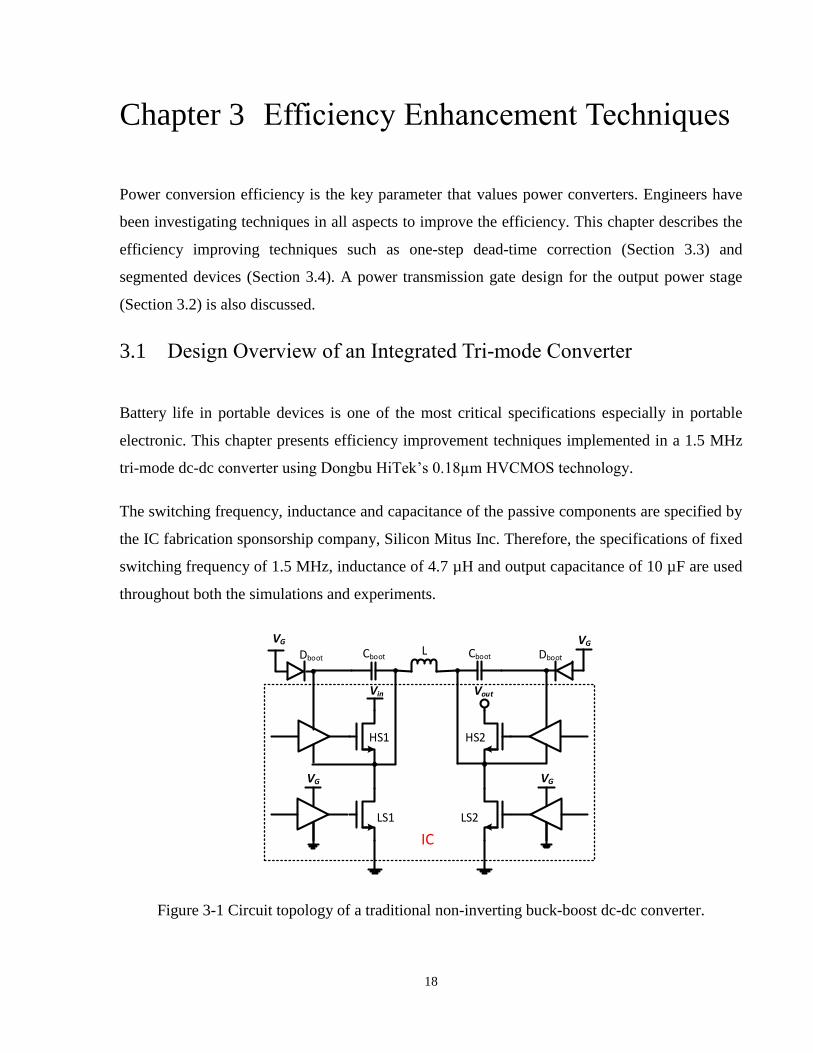
Figure 3-1 shows the circuit of a conventional non-inverting buck-boost dc-dc converter. The
output stage is a totem-pole design with the high side and low side devices implemented with a
pair of nMOS/nMOS devices [32]. All the components outside the dotted line are implemented
using discrete components on a printed circuit board (PCB). This topology is commonly used in
high voltage high current applications. Figure 2-3 shows a conventional non-inverting buck-
boost converter based on a pair of push-pull pMOS/nMOS structures. This configuration doesn’t
require the bootstrap circuits however it does has a larger die area overhead to accommodate
bigger pMOS transistors since their low hole surface mobility [32]. The proposed design is a
variant based on this topology as shown in Figure 3-2.
Vin
Vin
Vout
HS1
LS1 LS2
Vin
Vin
VinHS2_n HS2_p
Vx2Vx1
DT_1 DT_2
L
HS2
IC
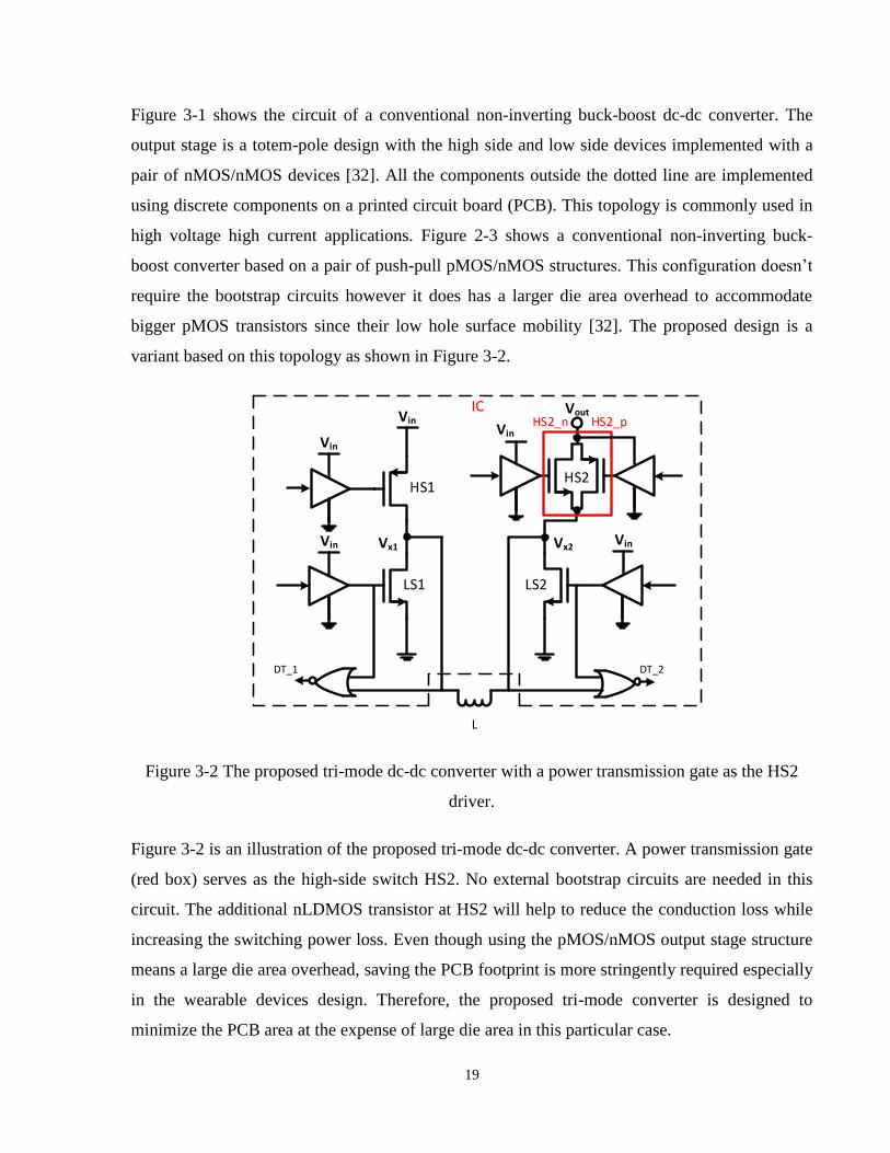
Figure 3-2 The proposed tri-mode dc-dc converter with a power transmission gate as the HS2
driver.
Figure 3-2 is an illustration of the proposed tri-mode dc-dc converter. A power transmission gate
(red box) serves as the high-side switch HS2. No external bootstrap circuits are needed in this
circuit. The additional nLDMOS transistor at HS2 will help to reduce the conduction loss while
increasing the switching power loss. Even though using the pMOS/nMOS output stage structure
means a large die area overhead, saving the PCB footprint is more stringently required especially
in the wearable devices design. Therefore, the proposed tri-mode converter is designed to
minimize the PCB area at the expense of large die area in this particular case.

20
In addition, two NOR gates are added to monitor the gate signals of the nLDMOS low side
devices and the switching nodes, Vx1 and Vx2, to facilitate the one-step dead-time correction
technique [24]. Finally, all the power devices are implemented in eight equally sized segments
that can be digitally activated on the fly. The benefits of these features will be illustrated in the
Section 3.4.
3.2 Power Transmission Gate
This section discusses the working principle of the power transmission gate (PTG) structure and
how the tri-mode converters can benefit from this technology. Simulation results are provided to
demonstrate its effectiveness.
3.2.1 Background and Introduction of Power Transmission Gate
A CMOS Transmission gate is comprised of two transistors, an n-channel MOSFET and a p-
channel MOSFET, connected in parallel. This structure is commonly used in digital circuits that
pass a logic signal with no voltage drop. The power transmission gate, likewise, adapts the same
idea to provide a current path with no significant power losses.
Vin en
HS2 inputpLDMOS
Vout
HS2
nLDMOS
Vout=1~5V
Vin=2.7~4.2V
Vout
Vx2
Vgs,n Vgs,p
Figure 3-3 Power transmission gate used as the high side driver, HS2.
Figure 3-3 shows the proposed power transmission gate and the operational ranges of the input
voltage and output voltage. The totem-pole design in Figure 3-1 needs two bootstrap circuits for
proper operation. A push-pull design (Figure 2-3) cannot work with Vout lower than 1.5V, given
21
that the Vth,p for the pLDMOS is 1.5V (see Figure 3-6), unless an external gate driver power
supply is provided. The benefits of using the power transmission gate are 1) save PCB footprint
overhead and parts count from not using bootstrap circuits in comparison with the totem pole
output stage converters, 2) save external gate driver voltage supply, 3) extend the output voltage
Vout range in comparison with the pull-push output stage converters. However, using this power
transmission gate will increase the die area overhead and incur a higher switching power loss.
The purpose of adapting this design in the tri-mode converter is to minimize the external
components and provide the output voltages lower than 1.5V.
P-well
OxideN-IMP
NBL (N-type)
N-well
P-IMPP-IMPSTIN-IMP
N-well
N-well
OxideP-IMP
NBL (N-type)
N-IMPN-IMPSTIP-IMP
P-well
Drain
STI
STI
DNW (N-type)
STI N-IMP
N-well
GateISO-
ring
ISO-
ring
Vout
ISO
P-epi
Butted
source
Butted
source
GateDrain
Vout Vx2
Vx2 VoutVgs,p
Vgs,n
P-well
OxideP-IMP STI N-IMP
N-well
STI
ISO-
ringGate
Drain
Vx2Vgs,p
P-IMP
DNW (N-type)
N-well
OxideN-IMP N-IMP STI P-IMP
P-well
Drain
STI STIN-IMP
N-well
Gate ISO-
ring
Vout
ISO
P-epi
VoutVgs,n
DPW (P-type) DNW (N-type)
(a) pLDMOS
(b) nLDMOS ISO
P-substrate
P-substrate
P-well
Figure 3-4 Cross-sectional diagrams of the power devices in the power transmission gate: (a)
pLDMOS and (b) nLDMOS ISO.
22
The cross-sectional diagrams for the pLDMOS and nLDMOS are shown in Figure 3-4. The 12V
pLDMOS cell (pch_ldm_12V) and the 12V nLDMOS ISO cell (nch_ldm_iso_12V) are selected
from Dongbu HiTek’s 0.18µm HVCMOS PDK to be implemented in the power transmission
gate. The diagram shows the intrinsic body-diodes formed in the p-n junctions. Both the
pLDMOS and nLDMOS are isolated by the isolation rings and the nLDMOS contains an
additional P-epi layer isolation ring. As a result, the P-wells containing the drain to source
channels are isolated from the P-substrate. Moreover, these power devices are also surrounded by
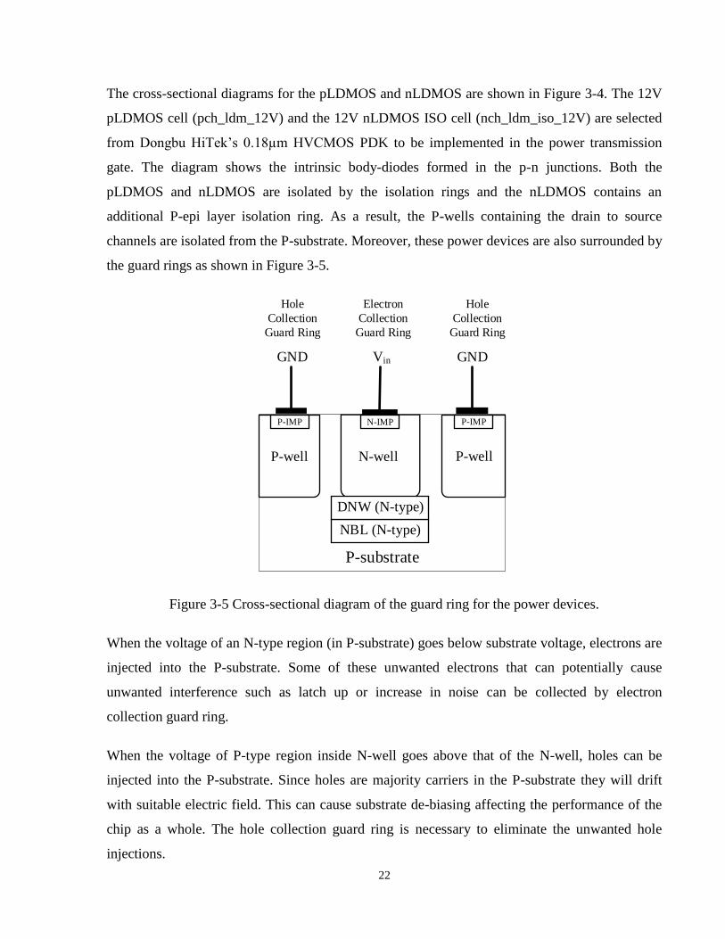
the guard rings as shown in Figure 3-5.
P-substrate
P-well
N-IMP
NBL (N-type)
N-well
P-IMP
GND
Hole
Collection
Guard Ring
P-well
P-IMP
Vin
DNW (N-type)
GND
Hole
Collection
Guard Ring
Electron
Collection
Guard Ring
Figure 3-5 Cross-sectional diagram of the guard ring for the power devices.
When the voltage of an N-type region (in P-substrate) goes below substrate voltage, electrons are
injected into the P-substrate. Some of these unwanted electrons that can potentially cause
unwanted interference such as latch up or increase in noise can be collected by electron
collection guard ring.
When the voltage of P-type region inside N-well goes above that of the N-well, holes can be
injected into the P-substrate. Since holes are majority carriers in the P-substrate they will drift
with suitable electric field. This can cause substrate de-biasing affecting the performance of the
chip as a whole. The hole collection guard ring is necessary to eliminate the unwanted hole
injections.
23
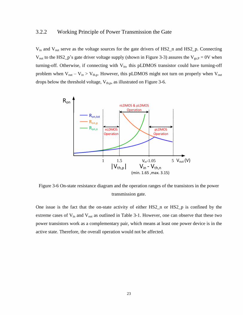
3.2.2 Working Principle of Power Transmission the Gate
Vin and Vout serve as the voltage sources for the gate drivers of HS2_n and HS2_p. Connecting
Vout to the HS2_p’s gate driver voltage supply (shown in Figure 3-3) assures the Vgs,P = 0V when
turning-off. Otherwise, if connecting with Vin, this pLDMOS transistor could have turning-off
problem when Vout – Vin > Vth,p. However, this pLDMOS might not turn on properly when Vout
drops below the threshold voltage, Vth,p, as illustrated on Figure 3-6.
Ron
Vout (V)
Ron,tot
Ron,p
Ron,n
|Vth,p| Vin - Vth,n(min. 1.65 ,max. 3.15)
1.5 Vin-1.051
nLDMOSOperation
pLDMOSOperation
5
nLDMOS & pLDMOSOperation
Figure 3-6 On-state resistance diagram and the operation ranges of the transistors in the power
transmission gate.
One issue is the fact that the on-state activity of either HS2_n or HS2_p is confined by the
extreme cases of Vin and Vout as outlined in Table 3-1. However, one can observe that these two
power transistors work as a complementary pair, which means at least one power device is in the
active state. Therefore, the overall operation would not be affected.
24
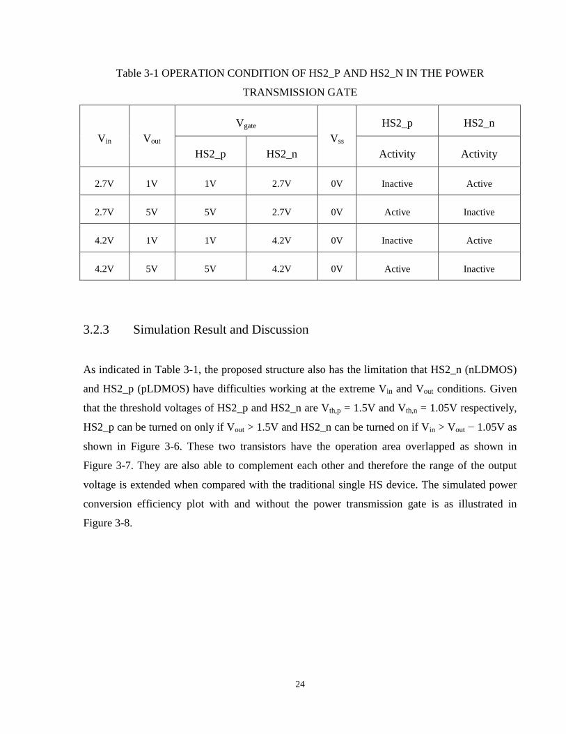
Table 3-1 OPERATION CONDITION OF HS2_P AND HS2_N IN THE POWER
TRANSMISSION GATE
Vin Vout
Vgate
Vss
HS2_p HS2_n
HS2_p HS2_n Activity Activity
2.7V 1V 1V 2.7V 0V Inactive Active
2.7V 5V 5V 2.7V 0V Active Inactive
4.2V 1V 1V 4.2V 0V Inactive Active
4.2V 5V 5V 4.2V 0V Active Inactive
3.2.3 Simulation Result and Discussion
As indicated in Table 3-1, the proposed structure also has the limitation that HS2_n (nLDMOS)
and HS2_p (pLDMOS) have difficulties working at the extreme Vin and Vout conditions. Given
that the threshold voltages of HS2_p and HS2_n are Vth,p = 1.5V and Vth,n = 1.05V respectively,
HS2_p can be turned on only if Vout > 1.5V and HS2_n can be turned on if Vin > Vout − 1.05V as
shown in Figure 3-6. These two transistors have the operation area overlapped as shown in
Figure 3-7. They are also able to complement each other and therefore the range of the output
voltage is extended when compared with the traditional single HS device. The simulated power
conversion efficiency plot with and without the power transmission gate is as illustrated in
Figure 3-8.

25
1
2
3
4
5
6
1 2 3 4 5 6 Vout
Vin
nLDMOS:Vin>Vout+1.05V
pLDMOS:
Vout>1.5V
nLDMOS ON
pLDMOS ON
Figure 3-7 On-state operation areas of power transmission gate.
An improvement of up to 8% can be observed. In addition, due to the fact that Vin and Vout are
serving as the supply voltage for the gate drivers, the range of input voltage would be constrained
severely without the use of the power transmission gate (PTG). Note that Figure 3-8 also shows
the power conversion efficiency as a function of Vin/Vout for all three modes of operation. A peak
efficiency of 94% is observed in boost mode.
Figure 3-8 Efficiency versus Vout/Vin in three modes with and without power transmission gate
enabled.
fsw=1.5MHz

26
3.3 One-step Dead-time correction
This section provides an introduction of the dead-time correction technique. The goal of this one-
step dead-time correction is to find the optimum dead-times where there is no cross conduction
or body-diode conduction. The algorithm of the one-step dead-time correction is implemented in
the FPGA by a visiting student, Silu Cheng.
NOR gate signal
(b)
Vin
VgS,p
VgS,n
Vx
(c)
NOR gate signal
(a)
NOR gate signal
Vx
Vgs,n
|Vgs,p|
NOR gate signal
tdt_r tdt_f tdt_r tdt_f
tdt_r tdt_f
Cross-condcution
Body-diode condcution
Zero effective dead-time
Vx
Vgs,n
|Vgs,p|
Vx
Vgs,n
|Vgs,p|Vth,p
Vth,n
Vth,p
Vth,n
Vth,p
Vth,n
L
IL
Body-diode condcution current
Figure 3-9 Switching diagrams for NOR gate body-diode conduction detection circuit: (a) dead-
time too short (b) proper dead-time (c) dead-time too long.

27
3.3.1 Background and Introduction of Dead-time Correction
Dead-time is the duration during which both the gate signals for the HS and LS devices are off.
This duration is normally user specified. Actually, the purpose of dead-time correction is to
eliminate the effective dead-time by adjusting the low side devices PWM generator, LS1 an LS2
in this case. Effective dead-time is defined as the duration when the turning-off device reaches its
gate threshold voltage (Vth,p) to when the turning-on device reaches its gate threshold voltage
(Vth,n) as shown in Figure 3-9. The effective dead-time is dependent on variations in threshold
voltage, gate resistance, gate capacitance, device operating voltage and current [34].
Cross-conductions happen when the high side and low side devices are both turned-on for a short
time (see Figure 3-9 (a)). At this time, Vin is short to the ground. A significant amount of current
goes through the devices resulting not only power losses but also a shoot-through current which
impacts the power efficiency and damage the devices. Body-diode conduction happens when an
excessively long dead-time is used such that the high side and low side devices are turned-off
simultaneously (see Figure 3-9 (c)). This unwanted scenario will result body-diode conduction
losses and reverse recovery losses as discussed in Section 2.4.2. The challenge in the proposed
dead-time correction circuit is to continuously update the dead-time such that the cross
conductions and body-diode conductions are always minimized as shown in Figure 3-9 (b).
In order to avoid the cross-conduction, a fixed dead-time is introduced to ensure that one device
is completely off before the other one is turned on [22]. However, if this dead-time is too long,
the body-diode may be forced to turn on to carry the output currents. This section introduces a
solution for the four-switch non-inverting dc-dc converters that predicts the optimized switching
dead-times and eliminates the cross-conductions and body-diode conductions on the fly. This
technique is originally proposed in a previous work which is based on a buck converter topology
[23]. This work extends the control algorithm to operate with the four-switch H-bridge output
stage (see Figure 3-10).
28
Vin
Vin
Vout
HS1HS2
LS1 LS2
Vin
Vin
VinHS2_n HS2_p
Vx2Vx1
HybridDPWM
Dead-time Eege
Detect
Pulse Width Measurement
HS1LS1
LS2HS2
DT_1 DT_2
DT_1
DT_2
Rising edge
Falling edge
tRising edge[n]
tFalling edge[n]
L
HS2
FPGA
Vgate_ls1 Vgate_ls2
IC
Figure 3-10 The proposed tri-mode dc-dc converter IC with dead-time correction.
3.3.2 Working Principle of Dead-time Correction
A one-step dead-time correction scheme is used to eliminate unwanted body-diode conductions
and cross-conductions [23], [24], [33]. By detecting and measuring the body-diode dead-times,
the circuit outputs the corrected gate signals that reduce the effective dead-time to zero.
The algorithm starts with a safe dead-times greater than 10ns (tdt_r1, tdt_f1, tdt_r2, tdt_f2) to avoid
cross-conduction and this dead-time correction scheme is also compatible with tri-mode
operation as shown in Figure 3-11. This section will focus on the buck-boost mode as an

29
extension to previous work [23]. In addition, the dead-time correction in buck-boost mode
includes the algorithm used in other modes.
HS2
tdt_r1 tdt_f1
tdt_r2 tdt_f2
Buck Mode Buck-boost Mode Boost Mode
LS2
HS1
LS1
Figure 3-11 DPWM outputs for the tri-mode converter in buck mode, buck-boost mode and
boost mode.
Two NOR gates are used to compare the low side gate-source voltages Vgs,ls1, Vgs,ls2 and the
drain-source voltages Vx1, Vx2, respectively, see Figure 3-10. In digital circuits, the NOR gate
outputs logic high signals where both input signals are equal to 0. Actually, body-diode
conductions can be considered as where Vgs,ls and Vx are equal to 0 in this setup as shown in
Figure 3-9 (c). Therefore, body-diode conduction can be identified and its duration measured
[35].
In order to measure the time length of the body-diode conduction, there are three cases that need
to be treated differently. Figure 3-12 shows the three cases that may occur in this dead-time
correction method:
a) Two pulses are generated which means that the body-diode conductions are at both
the rising edge and falling edge.
b) Only one pulse is found and it needs to be identified at which edge it is triggered
(rising edge is this case).
c) Only one pulse is found and it needs to be identified at which edge it is triggered
(falling edge in this case).
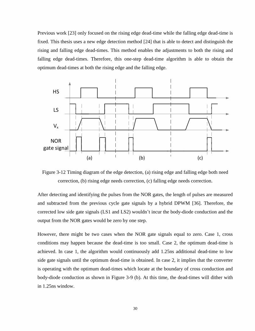
30
Previous work [23] only focused on the rising edge dead-time while the falling edge dead-time is
fixed. This thesis uses a new edge detection method [24] that is able to detect and distinguish the
rising and falling edge dead-times. This method enables the adjustments to both the rising and
falling edge dead-times. Therefore, this one-step dead-time algorithm is able to obtain the
optimum dead-times at both the rising edge and the falling edge.
NOR gate signal
Vx
LS
HS
(a) (b) (c)
Figure 3-12 Timing diagram of the edge detection, (a) rising edge and falling edge both need
correction, (b) rising edge needs correction, (c) falling edge needs correction.
After detecting and identifying the pulses from the NOR gates, the length of pulses are measured
and subtracted from the previous cycle gate signals by a hybrid DPWM [36]. Therefore, the
corrected low side gate signals (LS1 and LS2) wouldn’t incur the body-diode conduction and the
output from the NOR gates would be zero by one step.
However, there might be two cases when the NOR gate signals equal to zero. Case 1, cross
conditions may happen because the dead-time is too small. Case 2, the optimum dead-time is
achieved. In case 1, the algorithm would continuously add 1.25ns additional dead-time to low
side gate signals until the optimum dead-time is obtained. In case 2, it implies that the converter
is operating with the optimum dead-times which locate at the boundary of cross conduction and
body-diode conduction as shown in Figure 3-9 (b). At this time, the dead-times will dither with
in 1.25ns window.
31
3.4 Segmented Power Device Structure
Segmented power device structure is currently used in many SMPS converters [37], [38], [39],
[40], [41], [42], [43]. Segmented power device structure is a technology that divides the power
switching devices into several pieces/segments connected in parallel. Every segment is
comprised of identical MOSFET cells with different sizes. This technology allows the trade-off
between gate-drive loss and conduction loss in the power switching devices. The loss is
represented as:
(3.1)
The goal is to minimize this Ploss which is the sum of gate-drive loss and conduction loss in terms
of different output currents. Conduction loss and gate-drive loss are equally important in
determining the overall power conversion efficiency as shown in (2.3). On-resistance (Ron) and
gate capacitance (Cgs) determine the conduction loss and gate driving loss respectively. By
activating different number of segments of the power switches, Ron and Cgs can be adjusted to
achieve the lowest total power loss, Ploss. This would allow the converter to operate at the peak
efficiency for a wide range of loading conditions.
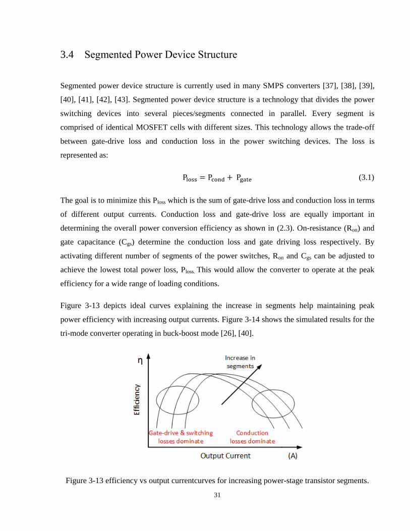
Figure 3-13 depicts ideal curves explaining the increase in segments help maintaining peak
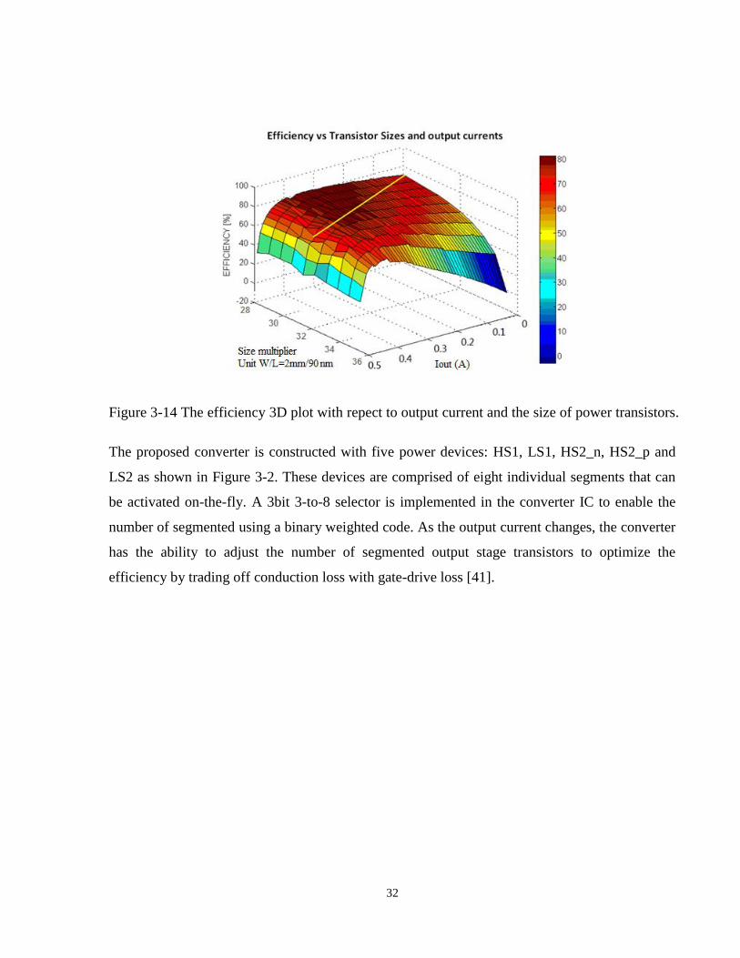
power efficiency with increasing output currents. Figure 3-14 shows the simulated results for the
tri-mode converter operating in buck-boost mode [26], [40].
Figure 3-13 efficiency vs output currentcurves for increasing power-stage transistor segments.
32
Figure 3-14 The efficiency 3D plot with repect to output current and the size of power transistors.
The proposed converter is constructed with five power devices: HS1, LS1, HS2_n, HS2_p and
LS2 as shown in Figure 3-2. These devices are comprised of eight individual segments that can
be activated on-the-fly. A 3bit 3-to-8 selector is implemented in the converter IC to enable the
number of segmented using a binary weighted code. As the output current changes, the converter
has the ability to adjust the number of segmented output stage transistors to optimize the
efficiency by trading off conduction loss with gate-drive loss [41].
33
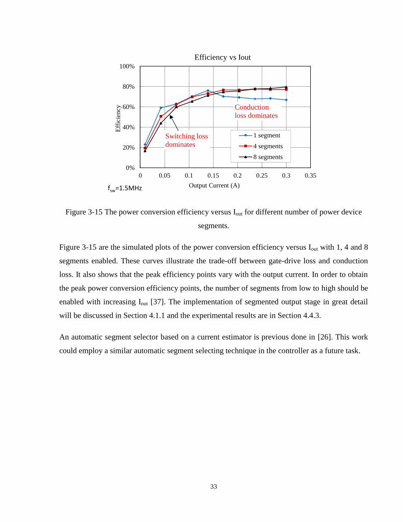
Figure 3-15 The power conversion efficiency versus Iout for different number of power device
segments.
Figure 3-15 are the simulated plots of the power conversion efficiency versus Iout with 1, 4 and 8
segments enabled. These curves illustrate the trade-off between gate-drive loss and conduction
loss. It also shows that the peak efficiency points vary with the output current. In order to obtain
the peak power conversion efficiency points, the number of segments from low to high should be
enabled with increasing Iout [37]. The implementation of segmented output stage in great detail
will be discussed in Section 4.1.1 and the experimental results are in Section 4.4.3.
An automatic segment selector based on a current estimator is previous done in [26]. This work
could employ a similar automatic segment selecting technique in the controller as a future task.
0%
20%
40%
60%
80%
100%
0 0.05 0.1 0.15 0.2 0.25 0.3 0.35
Eff
icie
ncy
Output Current (A)
Efficiency vs Iout
1 segment
4 segments
8 segments
Switching loss
dominates
Conduction
loss dominates
fsw=1.5MHz

34
3.5 Summary
Three power conversion efficiency improvement techniques is present in this chapter. The power
transmission gate in the output stage enables the dc-dc converter to eliminate bootstrap circuits
or external power supply. This design extends the output voltage range to Vout < 1.5V.
The one-step dead-time correction technique is used to eliminate the unwanted cross-conductions
and body-diode conductions. Therefore, the power efficiency is improved. This one-step dead-
time correction technique is implemented on a four-switch H-bridge output stage to differ from
previous work [23]. The segmented power devices technique is explained as it enables the circuit
to keep operating at the peak power efficiencies with different output currents. The experimental
results will be present in Chapter 4.
35
Chapter 4 IC Implementation and Experimental
Results
Section 4.1 describes the implementation of the tri-mode converter integrated circuit. The layout
optimization of the top layer metallization is explained in detail. The PCB implementation is
discussed in Section 4.2. The experimental results of the tri-mode operation, power transmission
gate, one-step dead-time correction and segmented power devices are provided in Sections 4.3
and 4.4.
4.1 IC Implementation
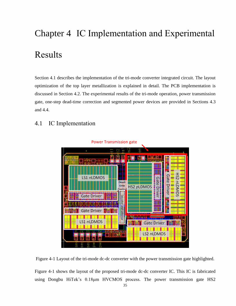
Power Transmission gate
Figure 4-1 Layout of the tri-mode dc-dc converter with the power transmission gate highlighted.
Figure 4-1 shows the layout of the proposed tri-mode dc-dc converter IC. This IC is fabricated
using Dongbu HiTek’s 0.18μm HVCMOS process. The power transmission gate HS2
36
(highlighted) combines with an nLDMOS and a pLDMOS power transistor that occupies 18% of
the total die area (1650 μm ×2300 μm). All other components are as labelled.
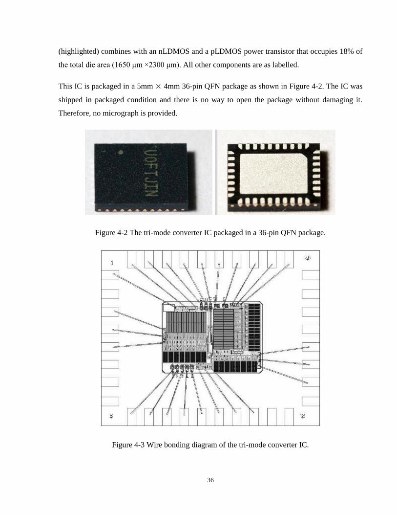
This IC is packaged in a 5mm × 4mm 36-pin QFN package as shown in Figure 4-2. The IC was
shipped in packaged condition and there is no way to open the package without damaging it.
Therefore, no micrograph is provided.
Figure 4-2 The tri-mode converter IC packaged in a 36-pin QFN package.
Figure 4-3 Wire bonding diagram of the tri-mode converter IC.

37
Figure 4-3 shows the wire-bonding diagram. This package is the smallest available QFN package
to fit the silicon die. The diameter of the copper bond-wire is 0.7μm. Gold bond-wire is not
available as an option.
4.1.1 Metallization Optimization of the Power Devices
At high output current, conduction losses dominate the total power loss in the power devices as
discussed in Section 2.4.1. Therefore, reducing the conduction loss is an important task in power
IC layout.
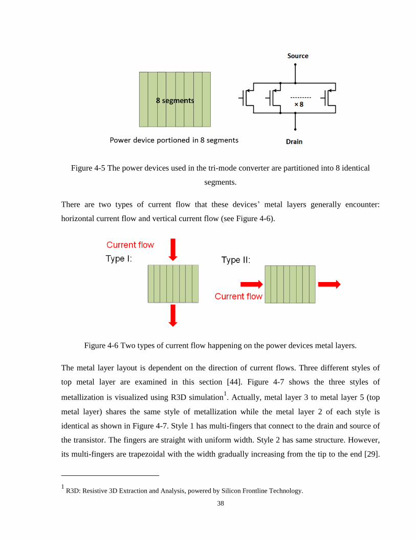
Figure 4-4 illustrates the placement of the power devices in the white boxes. All of the power
devices are partitioned into eight identical segments as shown in Figure 4-5. The following
simulations use the pLDMOS to demonstrate the metallization optimization results.
Figure 4-4 Top metal layer layout with the power devices labelled in white boxes.
38
Figure 4-5 The power devices used in the tri-mode converter are partitioned into 8 identical
segments.
There are two types of current flow that these devices’ metal layers generally encounter:
horizontal current flow and vertical current flow (see Figure 4-6).
Figure 4-6 Two types of current flow happening on the power devices metal layers.
The metal layer layout is dependent on the direction of current flows. Three different styles of
top metal layer are examined in this section [44]. Figure 4-7 shows the three styles of
metallization is visualized using R3D simulation1. Actually, metal layer 3 to metal layer 5 (top
metal layer) shares the same style of metallization while the metal layer 2 of each style is
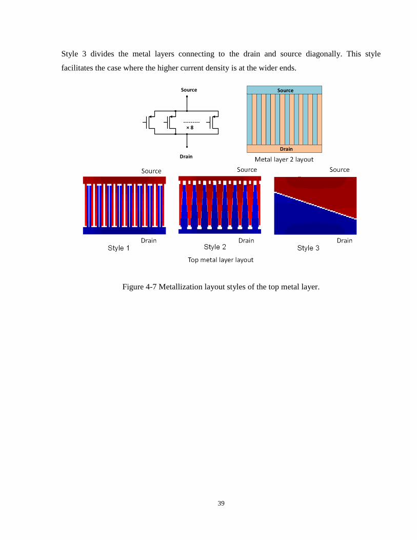
identical as shown in Figure 4-7. Style 1 has multi-fingers that connect to the drain and source of
the transistor. The fingers are straight with uniform width. Style 2 has same structure. However,
its multi-fingers are trapezoidal with the width gradually increasing from the tip to the end [29].
1 R3D: Resistive 3D Extraction and Analysis, powered by Silicon Frontline Technology.
39
Style 3 divides the metal layers connecting to the drain and source diagonally. This style
facilitates the case where the higher current density is at the wider ends.
Source
Drain
× 8
Source
Drain
Figure 4-7 Metallization layout styles of the top metal layer.
40
4.1.2 R3D Simulation for the Top Metal Layer of the Power Devices
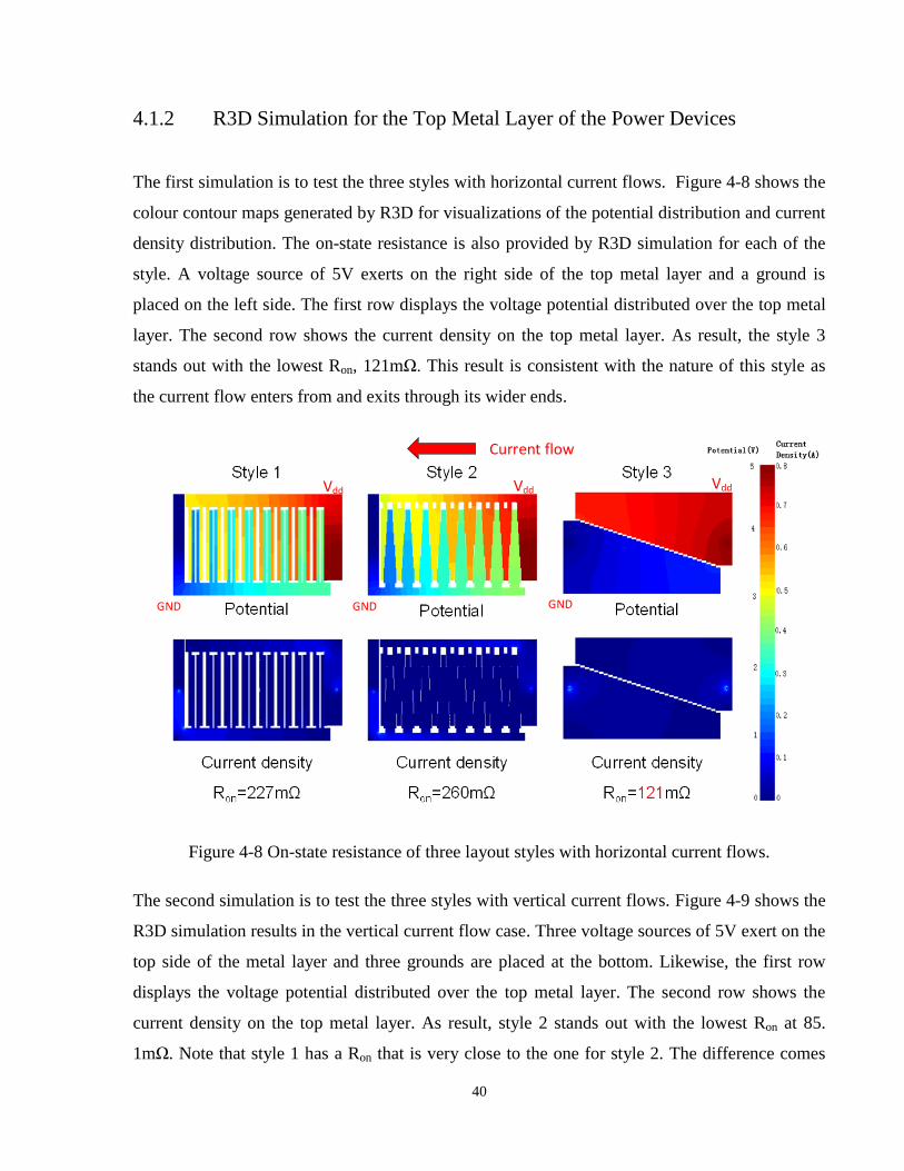
The first simulation is to test the three styles with horizontal current flows. Figure 4-8 shows the
colour contour maps generated by R3D for visualizations of the potential distribution and current
density distribution. The on-state resistance is also provided by R3D simulation for each of the
style. A voltage source of 5V exerts on the right side of the top metal layer and a ground is
placed on the left side. The first row displays the voltage potential distributed over the top metal
layer. The second row shows the current density on the top metal layer. As result, the style 3
stands out with the lowest Ron, 121mΩ. This result is consistent with the nature of this style as
the current flow enters from and exits through its wider ends.
Vdd
GND
Vdd
GND
Vdd
GND
Current flow
Figure 4-8 On-state resistance of three layout styles with horizontal current flows.
The second simulation is to test the three styles with vertical current flows. Figure 4-9 shows the
R3D simulation results in the vertical current flow case. Three voltage sources of 5V exert on the
top side of the metal layer and three grounds are placed at the bottom. Likewise, the first row
displays the voltage potential distributed over the top metal layer. The second row shows the
current density on the top metal layer. As result, style 2 stands out with the lowest Ron at 85.
1mΩ. Note that style 1 has a Ron that is very close to the one for style 2. The difference comes

41
from the fact that the current is not uniformly distributed over the multi-fingers. Actually the
current density decreases along with the fingers as it approaches to the tip.
Vdd
GND
Vdd
GND
Vdd
GND
Currentflow
Figure 4-9 On-state resistance of three layout styles with vertical current flows.
According to the current flow condition of each power device, the final metallization is
determined as shown in Figure 4-10. The HS1 is implemented with style 2 and other power
devices are implemented with style 3. Finally, the on-state resistances are measured as packaged
along with the bond-wires. They are summarized in Table 4-1.

42
Figure 4-10 Metallization layout for the proposed design.
Table 4-1 ON-STATE RESISTANCE OF EACH SEGMENT FOR THE POWER DEVICES
HS1 LS1 HS2
(PTG disabled)
HS2
(PTG enabled)
LS2
Segment(s)
enabled Ron (Ω)
1 0.599 0.536 0.616 0.366 0.614
2 0.354 0.331 0.359 0.229 0.393
3 0.284 0.256 0.291 0.194 0.322
4 0.245 0.223 0.255 0.179 0.281
5 0.224 0.198 0.233 0.159 0.259
6 0.212 0.187 0.215 0.145 0.242
7 0.204 0.174 0.208 0.137 0.230
8 0.201 0.170 0.203 0.133 0.222
43
4.2 Printed Circuit Board (PCB) Implementation
There are two versions of test PCBs designed to measure the power conversion efficiency with
and without one-step dead-time correction circuit. Commercial SMPS mainly operates with a
closed-loop (PID compensation) control to keep the output voltage constant and stable at a target
level. This closed-loop control is not required in this test. Therefore, the control loop is left out in
order to simplify the work. The inductor is placed on the bottom layer (not visible in the
diagrams) for both versions.
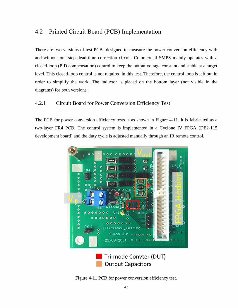
4.2.1 Circuit Board for Power Conversion Efficiency Test
The PCB for power conversion efficiency tests is as shown in Figure 4-11. It is fabricated as a
two-layer FR4 PCB. The control system is implemented in a Cyclone IV FPGA (DE2-115
development board) and the duty cycle is adjusted manually through an IR remote control.
Tri-mode Convter (DUT)
Vin
FPG
A H
edae
r
Vout
Output Capacitors
Figure 4-11 PCB for power conversion efficiency test.
44
The FPGA can manually control the duty cycle, the dead-times of the two sides of the H-bridge
output stage, the number of segments and enable the power transmission gate through a 2-row
40-pin header.
4.2.2 Test Board with One-Step Dead-time correction Circuit
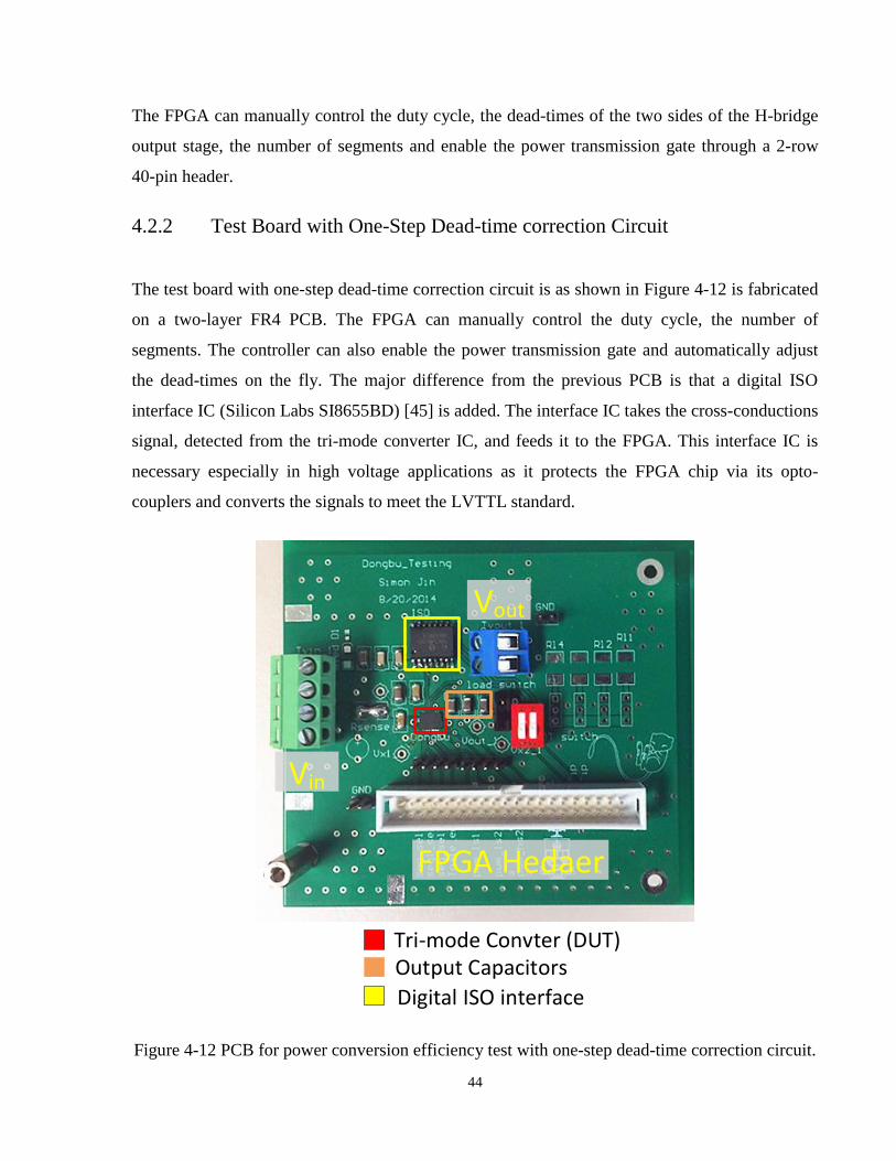
The test board with one-step dead-time correction circuit is as shown in Figure 4-12 is fabricated
on a two-layer FR4 PCB. The FPGA can manually control the duty cycle, the number of
segments. The controller can also enable the power transmission gate and automatically adjust
the dead-times on the fly. The major difference from the previous PCB is that a digital ISO
interface IC (Silicon Labs SI8655BD) [45] is added. The interface IC takes the cross-conductions
signal, detected from the tri-mode converter IC, and feeds it to the FPGA. This interface IC is
necessary especially in high voltage applications as it protects the FPGA chip via its opto-
couplers and converts the signals to meet the LVTTL standard.
Digital ISO interface
Tri-mode Convter (DUT)Output Capacitors
Vin
Vout
FPGA Hedaer
Figure 4-12 PCB for power conversion efficiency test with one-step dead-time correction circuit.

45
4.3 Tri-mode Operation
As explained in Chapter 2.4, the tri-mode converter will operate in the most power efficient
mode, depending on the input and output voltage [29], [30]. Due to the fact that lithium-ion
batteries drop their supply voltage while discharging, this experiment verifies that the tri-mode
converter can provide a 3.3V output voltage with the input Vin varying from 2.7V to 4.2V and a
constant output current of 0.2A. For this test, the power transmission gate is enabled and 6 out of
8 segments of the power devices in the output stage are enabled. This combination of parameters
is selected according to the results in Section 4.4.3 where the peak efficiency are mostly found
around Iout = 0.2A with 6 segments enabled.
The power conversion efficiency measured with Vin from 2.7V to 4.2V is as shown in Figure
4-13. This test imitates the scenario of a discharging battery: the converter switches from buck
mode to buck-boost mode (Figure 4-14) as the battery drops from 4.2V to 3.4V and subsequently
switches to boost mode (Figure 4-15) when Vin or Vbatt falls under 3.2V. The diagram clearly
labels the boundary of the modes to indicate at where the mode should be transitioned.
Figure 4-13 Power conversion efficiency of the tri-mode converter operating in three modes with
various input voltages.
60%
65%
70%
75%
80%
85%
90%
95%
100%
2.7 3.2 3.7 4.2
Eff
icie
ncy
Vin
Efficiency vs Vin
Buck Mode
Buck-Boost Mode
Boost Mode
Buck mode favorable
Buck-boost mode favorable
Boost mode favorable
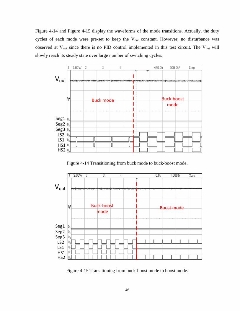
46
Figure 4-14 and Figure 4-15 display the waveforms of the mode transitions. Actually, the duty
cycles of each mode were pre-set to keep the Vout constant. However, no disturbance was
observed at Vout since there is no PID control implemented in this test circuit. The Vout will
slowly reach its steady state over large number of switching cycles.
Vout
Seg1Seg2Seg3LS2LS1HS1HS2
Buck mode Buck-boost mode
Figure 4-14 Transitioning from buck mode to buck-boost mode.
Vout
Seg1Seg2Seg3LS2LS1HS1HS2
Buck-boost mode
Boost mode
Figure 4-15 Transitioning from buck-boost mode to boost mode.
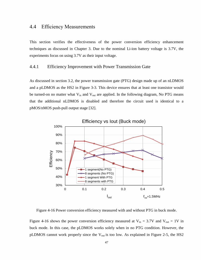
47
4.4 Efficiency Measurements
This section verifies the effectiveness of the power conversion efficiency enhancement
techniques as discussed in Chapter 3. Due to the nominal Li-ion battery voltage is 3.7V, the
experiments focus on using 3.7V as their input voltage.
4.4.1 Efficiency Improvement with Power Transmission Gate
As discussed in section 3.2, the power transmission gate (PTG) design made up of an nLDMOS
and a pLDMOS as the HS2 in Figure 3-3. This device ensures that at least one transistor would
be turned-on no matter what Vin and Vout are applied. In the following diagram, No PTG means
that the additional nLDMOS is disabled and therefore the circuit used is identical to a
pMOS/nMOS push-pull output stage [32].
Figure 4-16 Power conversion efficiency measured with and without PTG in buck mode.
Figure 4-16 shows the power conversion efficiency measured at Vin = 3.7V and Vout = 1V in
buck mode. In this case, the pLDMOS works solely when in no PTG condition. However, the
pLDMOS cannot work properly since the Vout is too low. As explained in Figure 2-5, the HS2
30%
40%
50%
60%
70%
80%
90%
100%
0 0.1 0.2 0.3 0.4 0.5
Eff
icie
ncy
Iout
Efficiency vs Iout (Buck mode)
1 segment(No PTG)
8 segments (No PTG)
1 segment With PTG
8 segments with PTG
fsw=1.5MHz

48
should be turned on all the time and therefore the power transmission gate can be enabled with
no additional switching power loss or gate-drive loss. Actually, the difference in efficiency is
quite obvious in the cases where Vout < 1.5V. As a result, the PTG is necessary in this tri-mode
converter if low output voltage is required.
Figure 4-17 shows the power conversion efficiency measured at Vin = 3.7V and Vout = 1.8V in
buck-boost mode. This particular output voltage is commonly used as the LVCMOS logic
interface level. Both the nLDMOS and pLDMOS are switching on and off properly. Enabling the
power transmission means adding an addition power transistor (nLDMOS). The switching power
loss and gate-drive losses would increase while the conduction power would decrease since the
total Ron is lower. As shown in Figure 4-17, the efficiency improved by power transmission gate
is more effective at heavy load region.
Figure 4-17 Power conversion efficiency measured in buck-boost mode with and without PTG
enabled.
As Vout approaches 5V, the converter will switch to boost mode. In this case, the circuit without
transmission gate would work fine. Figure 4-18 shows a relatively small improvement in the
power conversion efficiency. In this case, the nLDMOS still participates the current conduction
when the nLDMOS source voltage or Vx2 is on rising edge. In the light load condition (red
20%
30%
40%
50%
60%
70%
80%
90%
0 0.1 0.2 0.3 0.4
Eff
icie
ncy
Iout
Efficiency vs Iout (Buck-boost mode)
Without PTG 1 segment
Without PTG 8 segments
With PTG 1 segment
With PTG 8 segments
Switching losses and gate -drive losses dominate
Conduction losses dominate
fsw=1.5MHz
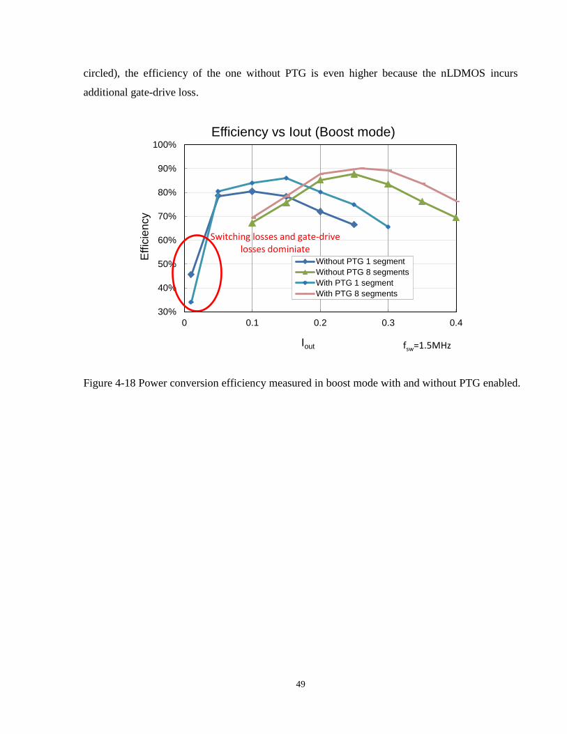
49
circled), the efficiency of the one without PTG is even higher because the nLDMOS incurs
additional gate-drive loss.
Figure 4-18 Power conversion efficiency measured in boost mode with and without PTG enabled.
30%
40%
50%
60%
70%
80%
90%
100%
0 0.1 0.2 0.3 0.4
Eff
icie
ncy
Iout
Efficiency vs Iout (Boost mode)
Without PTG 1 segment
Without PTG 8 segments
With PTG 1 segment
With PTG 8 segments
Switching losses and gate-drive losses dominiate
fsw=1.5MHz
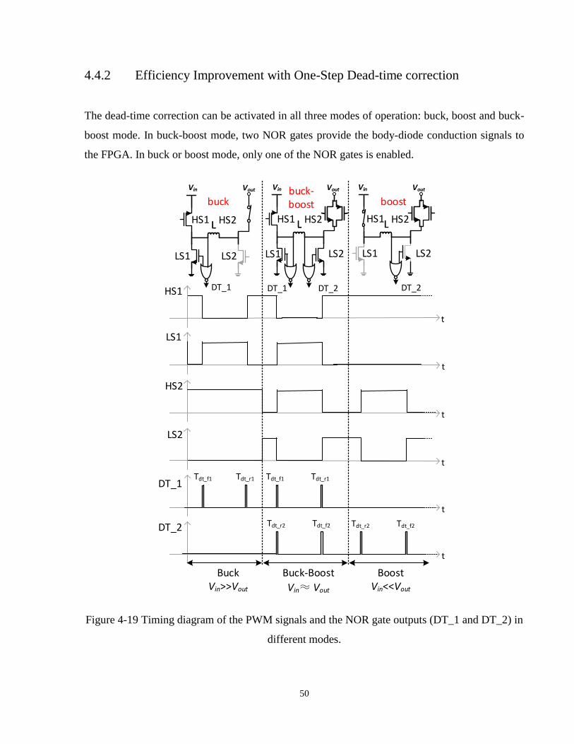
50
4.4.2 Efficiency Improvement with One-Step Dead-time correction
The dead-time correction can be activated in all three modes of operation: buck, boost and buck-
boost mode. In buck-boost mode, two NOR gates provide the body-diode conduction signals to
the FPGA. In buck or boost mode, only one of the NOR gates is enabled.
LHS1 L HS2
LS1 LS2
buck-boost
LS2
HS2
LS1
HS1
t
t
t
t
LHS1 L HS2
LS1 LS2
buck
LHS1
boost
L HS2
LS1 LS2
Vin Vout Vin Vout Vin Vout
DT_1 DT_1 DT_2 DT_2
DT_2
t
t
DT_1
BuckVin>>Vout
Buck-Boost
Vin Vout
BoostVin<<Vout
Tdt_f1 Tdt_r1 Tdt_f1 Tdt_r1
Tdt_r2 Tdt_f2 Tdt_r2 Tdt_f2
Figure 4-19 Timing diagram of the PWM signals and the NOR gate outputs (DT_1 and DT_2) in
different modes.
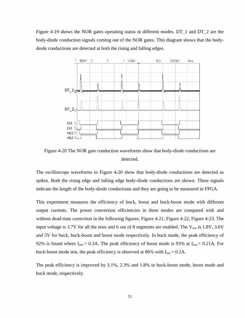
51
Figure 4-19 shows the NOR gates operating status in different modes. DT_1 and DT_2 are the
body-diode conduction signals coming out of the NOR gates. This diagram shows that the body-
diode conductions are detected at both the rising and falling edges.
DT_1
LS2
LS1
HS1HS2
DT_2
Figure 4-20 The NOR gate conduction waveforms show that body-diode conductions are
detected.
The oscilloscope waveforms in Figure 4-20 show that body-diode conductions are detected as
spikes. Both the rising edge and falling edge body-diode conductions are shown. These signals
indicate the length of the body-diode conductions and they are going to be measured in FPGA.
This experiment measures the efficiency of buck, boost and buck-boost mode with different
output currents. The power conversion efficiencies in three modes are compared with and
without dead-time correction in the following figures: Figure 4-21, Figure 4-22, Figure 4-23. The
input voltage is 3.7V for all the tests and 6 out of 8 segments are enabled. The Vout is 1.8V, 3.6V
and 5V for buck, buck-boost and boost mode respectively. In buck mode, the peak efficiency of
92% is found where Iout = 0.3A. The peak efficiency of boost mode is 93% at Iout = 0.21A. For
buck-boost mode test, the peak efficiency is observed at 86% with Iout = 0.2A.
The peak efficiency is improved by 3.1%, 2.3% and 1.8% in buck-boost mode, boost mode and
buck mode, respectively.
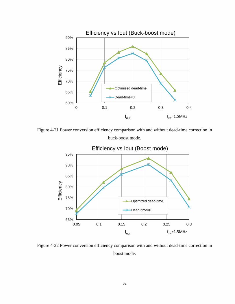
52
Figure 4-21 Power conversion efficiency comparison with and without dead-time correction in
buck-boost mode.
Figure 4-22 Power conversion efficiency comparison with and without dead-time correction in
boost mode.
60%
65%
70%
75%
80%
85%
90%
0 0.1 0.2 0.3 0.4
Eff
icie
ncy
Iout
Efficiency vs Iout (Buck-boost mode)
Optimized dead-time
Dead-time=0
fsw=1.5MHz
65%
70%
75%
80%
85%
90%
95%
0.05 0.1 0.15 0.2 0.25 0.3
Eff
icie
ncy
Iout
Efficiency vs Iout (Boost mode)
Optimized dead-time
Dead-time=0
fsw=1.5MHz
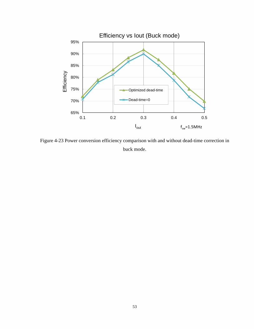
53
Figure 4-23 Power conversion efficiency comparison with and without dead-time correction in
buck mode.
65%
70%
75%
80%
85%
90%
95%
0.1 0.2 0.3 0.4 0.5
Eff
icie
ncy
Iout
Efficiency vs Iout (Buck mode)
Optimized dead-time
Dead-time=0
fsw=1.5MHz
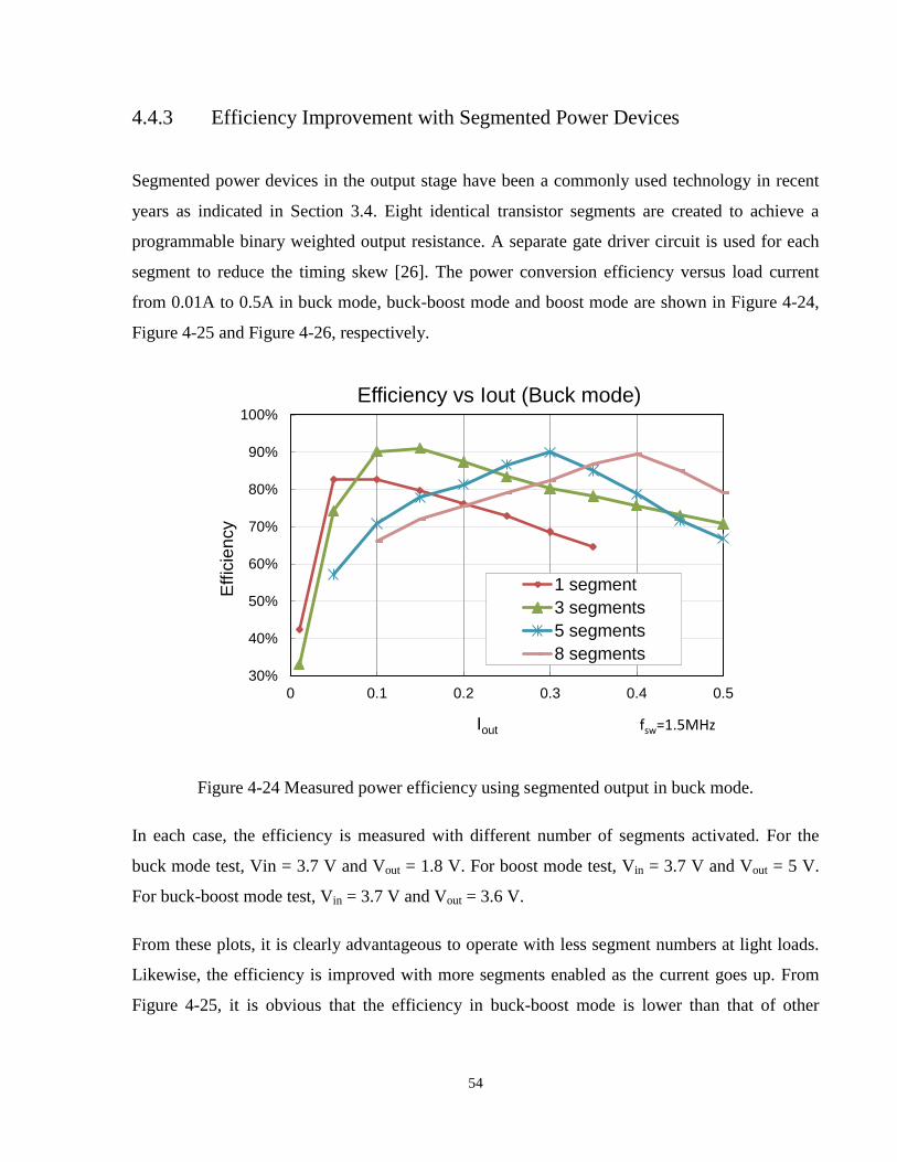
54
4.4.3 Efficiency Improvement with Segmented Power Devices
Segmented power devices in the output stage have been a commonly used technology in recent
years as indicated in Section 3.4. Eight identical transistor segments are created to achieve a
programmable binary weighted output resistance. A separate gate driver circuit is used for each
segment to reduce the timing skew [26]. The power conversion efficiency versus load current
from 0.01A to 0.5A in buck mode, buck-boost mode and boost mode are shown in Figure 4-24,
Figure 4-25 and Figure 4-26, respectively.
Figure 4-24 Measured power efficiency using segmented output in buck mode.
In each case, the efficiency is measured with different number of segments activated. For the
buck mode test, Vin = 3.7 V and Vout = 1.8 V. For boost mode test, Vin = 3.7 V and Vout = 5 V.
For buck-boost mode test, Vin = 3.7 V and Vout = 3.6 V.
From these plots, it is clearly advantageous to operate with less segment numbers at light loads.
Likewise, the efficiency is improved with more segments enabled as the current goes up. From
Figure 4-25, it is obvious that the efficiency in buck-boost mode is lower than that of other
30%
40%
50%
60%
70%
80%
90%
100%
0 0.1 0.2 0.3 0.4 0.5
Eff
icie
ncy
Iout
Efficiency vs Iout (Buck mode)
1 segment
3 segments
5 segments
8 segments
fsw=1.5MHz

55
modes. This is due to the fact that four power devices are switching simultaneously in this mode
which causes significant amount of switching power losses.
Figure 4-25 Power conversion efficiency with segmented output stage in buck-boost mode.
Figure 4-26 Power conversion efficiency with segmented output stage in boost mode.
20%
30%
40%
50%
60%
70%
80%
90%
0 0.1 0.2 0.3 0.4
Eff
icie
ncy
Iout
Efficiency vs Iout (Buck-boost mode)
1 segment
3 segments
6 segments
8 segments
fsw=1.5MHz
20%
30%
40%
50%
60%
70%
80%
90%
100%
0 0.1 0.2 0.3 0.4
Eff
icie
ncy
Iout
Efficiency vs Iout (Boost mode)
1 segment
3 segments
6 segments
8 segments
fsw=1.5MHz

56
In conclusion, the segmented power devices implemented in this tri-mode converter effectively
improve the power conversion efficiency with various output currents. To better serve this
segmented power device feature, an automatic segment selector and an integrated PDI control
system [26] should be considered in future designs.
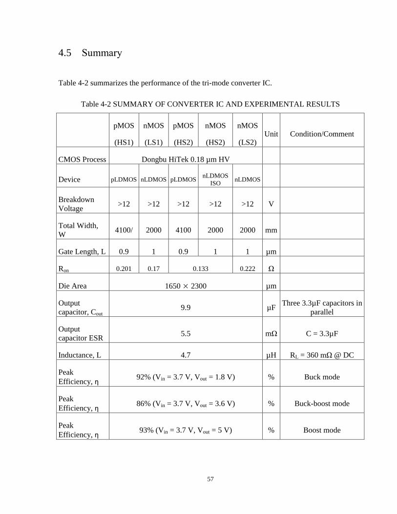
57
4.5 Summary
Table 4-2 summarizes the performance of the tri-mode converter IC.
Table 4-2 SUMMARY OF CONVERTER IC AND EXPERIMENTAL RESULTS
pMOS
(HS1)
nMOS
(LS1)
pMOS
(HS2)
nMOS
(HS2)
nMOS
(LS2) Unit Condition/Comment
CMOS Process Dongbu HiTek 0.18 µm HV
Device pLDMOS nLDMOS pLDMOS nLDMOS
ISO nLDMOS
Breakdown
Voltage >12 >12 >12 >12 >12 V
Total Width,
W 4100/ 2000 4100 2000 2000 mm
Gate Length, L 0.9 1 0.9 1 1 µm
Ron 0.201 0.17 0.133 0.222 Ω
Die Area 1650 × 2300 µm
Output
capacitor, Cout 9.9 µF
Three 3.3µF capacitors in
parallel
Output
capacitor ESR 5.5 mΩ C = 3.3µF
Inductance, L 4.7 µH RL = 360 mΩ @ DC
Peak
Efficiency, η 92% (Vin = 3.7 V, Vout = 1.8 V) % Buck mode
Peak
Efficiency, η 86% (Vin = 3.7 V, Vout = 3.6 V) % Buck-boost mode
Peak
Efficiency, η 93% (Vin = 3.7 V, Vout = 5 V) % Boost mode
58
Chapter 5 Conclusion and Future Tasks
A tri-mode dc-dc converter design is presented in this work with a unique power transmission
gate design on power devices and two efficiency enhancement techniques. This chapter
summarizes the contribution of the thesis and talks about the work needs to be done in the future.
5.1 Thesis Summary and Contributions
With the development of portable electronic devices, high power components such as LCD
screens, microprocessors, WIFI modules, etc. with different supply voltages are needed. The
stringent demands of portable devices power management solution required high efficiency,
battery powered, small, step-up and down dc-dc converters.
This thesis proposes a power transmission gate implemented in a tri-mode dc-dc converter. The
advantages of using a power transmission gate as the high side driver are also demonstrated. A
dead-time correction technique is implemented in the proposed tri-mode converter IC based on a
previous work [23]. With the help of another visiting student, Silu Cheng, who implemented the
one-step dead-time correction algorithm in FPGA, improvements are made including double
edge dead-time detection and H-bridge output stage implementation.
The tri-mode dc-dc converter is able to accept lithium-ion battery input voltage, Vin from 2.7V to
4.2V and produces an output, Vout ranging from 1V to 5V with a fixed switching frequency of
1.5MHz. Facilitated by segmented power device technique and tri-mode circuit design, the
proposed dc-dc converter can operate in buck, boost or buck-boost mode while maintaining peak
efficiency over different output currents, up to 0.5A. In conclusion, by incorporating the tri-mode
operation and segmented power device technique, the converter is able to achieve a peak
efficiency of 93% in boost mode. And the peak efficiencies of buck and buck-boost mode are
found at 92% and 86% respectively. A comparison table (Table 5-1) is provided to show the
performance of this work.

59
Table 5-1 COMPARISON TABLE WITH OTHER WORKS
This Work [25] [29] [30]
Topology Non-inverting
Buck-boost
Non-inverting
Buck-boost
Non-inverting
Buck-boost
Non-inverting
Buck-boost
Process Dongbu HiTek
0.18 µm HV
0.5μm CMOS
process
0.18μm CMOS
process N/A
Peak
Efficiency 93% 87% 91% 95%
Die area 1650µm ×
2300µm N/A
1650µm ×
2500µm N/A
Input voltage 2.7V-4.2V 3V-5.2V 2.7V-5.5V 2.5V-5V
Output voltage 1V-5V N/A 0V-5V 2.5V-5V
Inductance 4.7μH 1μH 1μH 10μH
Switching
frequency 1.5MHz 2MHz 2.5MHz 1MHz
Max output
current 0.5A 1.2A 2A 2A
Integrated PID
controller No Yes Yes Yes

60
5.2 Future Work
In this thesis, only the power output stage of the proposed tri-mode dc-dc converter is
implemented on a monolithic IC. However, all the control processes were implemented in FPGA.
Also, the current design only involved the open loop control with no PID compensation
implemented. The following topics may be further studied in the future:
1. A closed-loop circuit could be implemented in the next tape-out. The efficiency test
including the control circuits would reflect the power conversion efficiency of the power
management IC. The most challenging part is to incorporate the PID control, dead-time
correction and automatic segment control working simultaneously.
2. A current estimator [26] could be further investigated and implemented. A low power
dissipation current estimator is to evaluate the current through the inductor to determine how
many segments should be enabled as part of the power device segment control circuit.
3. Pulse frequency modulation (PFM) should be also implemented if the converter needs to
operate in light load situation. As extending the battery life in portable device is critically
important. PFM as the power saving in stand-by mode is a necessity.
4. Hybrid inductor package design [38] could be considered. The hybrid inductor package is to
pack a miniature inductor with a ferrite substrate. The trend in the portable applications
especially in wearable devices is to miniaturize the size and reduce the weight. If the size of
the inductive component could be further reduced, more space would be reserved for the
battery and thus extending the battery life.
61
References
[1] A. Stratakos, S. Sanders, and R. Brodersen, “A low-voltage CMOS dc-dc converter for a
portable battery-operated system,” in IEEE Power Electronics Specialists Conference,
1993 Rec., vol. 1, pp. 619-626, Jun. 1994.
[2] T. DeLurio, G.e Hall, J. Jones, “Manage the slippery slope of the portable equipment
power chain,” Summit Microelectronics, Internet:
http://www.eetimes.com/document.asp?doc_id=1273057 [2005].
[3] Y. Katayama, M. Edo, T. Denta, T. Kawashima, T. Ninomiya, “Optimum design method
of CMOS IC for dc-dc converter that integrates power stage MOSFETs,” 2004 IEEE
Power Electronics Specialists Conference (PESC 2004), Aachen, Vol.6, pp. 4486-4491,
Jun. 20-25, 2004.
[4] H. J. Zhang, “Basic Concepts of Linear Regulator and Switching,” Linear Technology
Application Note 140 (AN140), Oct. 2013.
[5] T. Piessens, A. Bakker, “Charge Pump and Capacitive DCDC Converter Design”, ISSCC
2014 Tutorial, San Franscisco, CA, Feb. 9th
, 2014.
[6] V. W.S. Ng, “Switched Capacitor dc-dc Converter: Superior where the Buck Converter
has Dominated”, University of California at Berkeley, Ph.D thesis, Aug. 17, 2011.
[7] A. Kushnerov, “High-Efficiency Self-Adjusting Switched Capacitor dc-dc Converter
with Binary Resolution. Electronics”, Ben-Gurion University of the Negev, 2010.
[8] Y. Kaiwei, “High-frequency and high-performance VRM design forthe next generations
of processors,” Ph.D. thesis, VirginiaPolytechnic Institute and State University, 2004.
[9] R. Erickson, D. Maksimovic, “Fundamentals of power electronics,” Kluwer Academic,
2001.
[10] Chipworks, “ Inside the Nike+ FuelBand…Nike chip inside!,” Internet:
http://www.chipworks.com/en/technical-competitive-analysis/resources/blog/inside-the-
nike-fuelband-nike-chip-inside/ [Feb. 21st, 2013].
[11] iFIXIT, “Motorola Moto 360 Teardown,” Internet:
https://www.ifixit.com/Teardown/Motorola+Moto+360+Teardown/2889, [Sep.9th, 2014].
[12] iFIXIT, “ Oculus Rift Development Kit 2 Teardown,” Internet:
https://www.ifixit.com/Teardown/Oculus+Rift+Development+Kit+2+Teardown/27613,
[Aug. 1st, 2014].
[13] iFIXIT, “ Samsung Gear Live Teardown,” Internet:
https://www.ifixit.com/Teardown/Samsung+Gear+Live+Teardown/27038, [Jul. 8th,
2014].
[14] iFIXIT, “ LG G Watch Teardown,” Internet:
https://www.ifixit.com/Teardown/LG+G+Watch+Teardown/27037, [Jul. 15th, 2014].
[15] iFIXIT, “ Samsung Gear Fit Teardown,” Internet:
https://www.ifixit.com/Teardown/Samsung+Gear+Fit+Teardown/24029, [Apr. 13th,
2014].

62
[16] iFIXIT, “Samsung Gear 2 Teardown,” Internet:
https://www.ifixit.com/Teardown/Samsung+Gear+2+Teardown/23990, [Apr. 9th, 2014].
[17] S. M. Ahsanuzzaman, J. Blackman, T. McRae, A. Prodic, “A low-volume power
management module for portable applications based on a multi-output switched-capacitor
circuit,” Applied Power Electronics Conference and Exposition (APEC 2013), Long
Beach, CA, pp. 1473-1479, Mar. 17-21, 2013.
[18] P. Henry, “New Advances in Portable Electronics,” in APEC Plenary Session, March
2009.
[19] MT-098, “Low Voltage Logic Interfacing”, Analog Devices.
[20] WP-01071-1.0, “Voltage Regulator Selection for FPGAs”, Altera Corporation.
[21] J. F. Wakerly, “Digital Design: Principles and Practices”, Sec 3.13, pp. 168.
[22] B. Sahu, G. Rincon-Mora, “A low voltage, dynamic, noninverting, synchronous buck-
boost converter for portable applications,” IEEE Transactions on Power Electronics, Vol.
19, No. 2, Mar. 2004.
[23] A. Zhao, A.A. Fomani, W.T. Ng, "One-step digital dead-time correction for dc-dc
converters," Applied Power Electronics Conference and Exposition (APEC 2010), Palm
Spring, CA, pp.132-137, Feb. 21-25, 2010.
[24] S. Cheng, S. Yao, G. Jin, W.T. Ng, “Digital Controlled Dead-time for Tri-mode Buck-
boost dc-dc Converters”, 2014 IEEE 12th International Conference on Solid-State and
Integrated Circuit Techonolgy (ICSICT 2014), pp. 1580-1582, Guilin, China, 2014.
[25] S. Bang, D. Swank, A. Rao, W. McIntyre, Q. Khan, P.K. Hanumolu, "A 1.2A 2MHz tri-
mode Buck-Boost LED driver with feed-forward duty cycle correction," Custom
Integrated Circuits Conference (CICC 2010), pp.19-22, Sep. 225-228, 2010.
[26] O. Trescases, "Integrated Power-Supplies for Portable Applications," University of
Toronto, PhD Thesis 2007.
[27] E Rogers, “Understanding buck-boost power stages in switch mode power supplies,”
Texas Instrument literature number SLVA059A.
[28] M. Wens, M. Steyaert, “Design and Implementation of Fully-Integrated Inductive dc-dc
Converters in Standard CMOS,” Springer Science & Business Media, pp. 41, May 10,
2011.
[29] P. Malcovati, M. Belloni, F. Gozzini, C. Bazzani, A. Baschirotto, “A 0.18μm CMOS
91%-efficiency 0.1-to-2A scalable buck-boost dc-dc converter for LED drivers,” IEEE
Int. Solid-State Circuits Conference Digest of Technical Papers (ISSCC 2012), San
Francisco, CA, pp.280-282, Feb. 19-23, 2012.
[30] M. Gaboriault, A. Notman, "A high efficiency, Non-inverting, buck-boost dc-dc
converter," Applied Power Electronics Conference and Exposition (APEC 2004), vol.3,
pp.1411-1415, 2004.
[31] C. S. Mitter, "Device Consideration for High Current, Low Voltage Synchronous Buck
Regulators," in WESCON, pp. 281-288, 1997.

63
[32] W. T. Ng, O. Trescases, G. Wei, "Output Stages for Integrated dc-dc Converters and
Power ICs," Electron Devices and Solid-State Circuits (EDSSC 2007), pp.91-94, Dec. 20-
22 2007.
[33] A. Zhao, A. Shorten, H. Nishio, W.T. Ng, “An Integrated dc-dc Converter with Digital
One-step Dead-time Correction”, 22nd
Internation Symposium on Power Semiconductor
Devices & ICs (ISPSD 2010), pp. 57-60, Jun. 6-10, 2010.
[34] J. Strydom, D. Reusch, “Dead-Time Optimization for Maximum Efficiency”, EPC Corp.,
pp.1-2. Internet: http://epc-co.com/epc/documents/papers/Dead-
Time%20Optimization%20for%20Maximum%20Efficiency.pdf [2013].
[35] A. Zhao, “Efficiency Enhancement Techniques for Switched Mode Power Electronics,”
University of Toronto, MASc Thesis 2011.
[36] V. Yousefzadeh, T. Takayama, D. Maksimovic, “Hybrid DPWM with Digital Delay-
Locked Loop,” '06. IEEE Workshops on Computers in Power Electronics (COMPEL
2006), Troy, NY, pp. 142-148, Jul. 16-19, 2006.
[37] W.T. Ng, M. Chang, A. Yoo, J. Langer, T. Hedquist, H. Schweiss, “High Speed CMOS
Output Stage for Integrated dc-dc Converters”, 9th International Conference on Solid-
State and Integrated-Circuit Technology (ICSICT 2008), pp. 1909-1912, Oct. 20-23,
2008.
[38] O. Trescases, W. T. Ng, H. Nishio, M. Edo, T. Kawashima, "A Digitally Controlled dc-
dc Converter Module with a Segmented Output Stage for Optimized Efficiency," 2006
Power Semiconductor Devices and IC's (ISPSD 2006), pp.373-376, June 4-8, 2006.
[39] A. A. Fomani, A. Shorten, W. T. Ng, “An integrated segmented gate driver with
adjustable driving capability,” 2010 IEEE Energy Conversion Congress and Exposition
(ECCE 2010), Atlanta, GA, pp. 2430-2433, Sept. 12-16, 2010.
[40] A. Parayandeh, A. Prodic, “Digitally controlled low-power dc-dc converter with
segmented output stage and gate charge based instantaneous efficiency optimization,” '09.
IEEE Energy Conversion Congress and Exposition (ECCE 2009), San Jose, CA,
pp.3870-3875, Sept. 20-24, 2009.
[41] A. Parayandeh, A. Prodic, "Digitally Controlled Low-Power dc-dc Converter with
Instantaneous On-Line Efficiency Optimization," 2009 Applied Power Electronics
Conference and Exposition (APEC 2009), pp.159-163, Feb 15-19, 2009.
[42] W. T. Ng, O. Trescases, G. Wei, "Output Stages for Integrated dc-dc Converters and
Power ICs," Electron Devices and Solid-State Circuits (EDSSC 2007), pp.91-94, 20-22
Dec. 2007.
[43] O. Trescases, N. Rahman, A. Prodi W. T. Ng, “A 1V buck converter IC with hybrid
current-mode control and a charge-pump DAC,” 2008 IEEE Power Electronics
Specialists Conference (PESC 2008), Rhodes, pp.1122-1128, Jun. 15-19, 2008.
[44] A. Hastings, “The Art of Analog Layout”, Prentice Hall; 2 edition (July 4, 2005), Pp.
410-416.

64
[45] Silicon Labs, “LOW POWER FIVE-CHANNEL DIGITAL ISOLATOR”, Internet:
https://www.silabs.com/Support%20Documents%2fTechnicalDocs%2fSi865x.pdf [Sep.
2013].

65
Copyright Acknowledgements
Part of Chapter 3 is a reprint from the following publication:
G. Jin, W.T. Ng, “An Integrated Tri-mode Non-inverting Buck-Boost dc-dc Converter with
Segmented Power Devices and Power Transmission Gate Structure,” in International
Symposium on Power Semiconductor Devices and IC's (ISPSD 2014), Waikoloa, Hi, Jun. 15-
19, pp. 201-204, 2014.z