Embed Size (px)
Citation preview
University of Nebraska - LincolnDigitalCommons@University of Nebraska - Lincoln
Faculty Publications -- Chemistry Department Published Research - Department of Chemistry
2016
Effect of Synthesis on Quality, Electronic Propertiesand Environmental Stability of IndividualMonolayer Ti3C2 MXene FlakesAlexey LipatovUniversity of Nebraska-Lincoln, [email protected]
Mohamed H. AlhabebDrexel University, [email protected]
Maria R. LukatskayaDrexel University, [email protected]
Alex J. BosonUniversity of Nebraska-Lincoln, [email protected]
Yury GogotsiDrexel University, [email protected]
See next page for additional authors
Follow this and additional works at: http://digitalcommons.unl.edu/chemfacpub
Part of the Materials Chemistry Commons
This Article is brought to you for free and open access by the Published Research - Department of Chemistry at DigitalCommons@University ofNebraska - Lincoln. It has been accepted for inclusion in Faculty Publications -- Chemistry Department by an authorized administrator ofDigitalCommons@University of Nebraska - Lincoln.
Lipatov, Alexey; Alhabeb, Mohamed H.; Lukatskaya, Maria R.; Boson, Alex J.; Gogotsi, Yury; and Sinitskii, Alexander, "Effect ofSynthesis on Quality, Electronic Properties and Environmental Stability of Individual Monolayer Ti3C2 MXene Flakes" (2016).Faculty Publications -- Chemistry Department. 131.http://digitalcommons.unl.edu/chemfacpub/131

AuthorsAlexey Lipatov, Mohamed H. Alhabeb, Maria R. Lukatskaya, Alex J. Boson, Yury Gogotsi, and AlexanderSinitskii
This article is available at DigitalCommons@University of Nebraska - Lincoln: http://digitalcommons.unl.edu/chemfacpub/131
L ipatov & Alhabeb , e t a l . in Advanced Electronic Mater ials 2 (2016 ) 1
Published in Advanced Electronic Materials 2 (2016), 1600255. doi 10.1002/aelm.201600255 Copyright © 2016 WILEY-VCH Verlag GmbH & Co. Used by permission. Submitted July 2, 2016; revised July 26, 2016; published November 2, 2016
Effect of Synthesis on Quality, Electronic Properties and Environmental Stability of Individual Monolayer Ti3C2 MXene Flakes
Alexey Lipatov,1 Mohamed Alhabeb,2,3 Maria R. Lukatskaya,2,3 Alex Boson,1
Yury Gogotsi,2,3 and Alexander Sinitskii 1,4
1 Department of Chemistry, University of Nebraska–Lincoln, Lincoln, NE 68588, USA 2 Department of Materials Science and Engineering, Drexel University, Philadelphia, PA
19104, USA3 A. J. Drexel Nanomaterials Institute, Drexel University, Philadelphia, PA 19104, USA 4 Nebraska Center for Materials and Nanoscience, University of Nebraska–Lincoln, Lincoln,
NE 68588, USA Corresponding authors — A. Sinitskii, email [email protected] ; Y. Gogotsi, email [email protected]
Abstract 2D transition metal carbide Ti3C2Tx (T stands for surface termination), the most widely studied MXene, has shown outstanding electrochemical properties and promise for a number of bulk applications. However, electronic properties of individual MXene flakes, which are important for understanding the potential of these materials, re-main largely unexplored. Herein, a modified synthetic method is reported for pro-ducing high-quality monolayer Ti3C2Tx flakes. Field-effect transistors (FETs) based on monolayer Ti3C2Tx flakes are fabricated and their electronic properties are measured. Individual Ti3C2Tx flakes exhibit a high conductivity of 4600 ± 1100 S cm−1 and field-effect electron mobility of 2.6 ± 0.7 cm2 V−1 s−1. The resistivity of multilayer Ti3C2Tx films is only one order of magnitude higher than the resistivity of individual flakes, which indicates a surprisingly good electron transport through the surface termi-nations of different flakes, unlike in many other 2D materials. Finally, the fabricated FETs are used to investigate the environmental stability and kinetics of oxidation of Ti3C2Tx flakes in humid air. The high-quality Ti3C2Tx flakes are reasonably stable and remain highly conductive even after their exposure to air for more than 24 h. It is demonstrated that after the initial exponential decay the conductivity of Ti3C2Tx flakes linearly decreases with time, which is consistent with their edge oxidation.
digitalcommons.unl.edu
L ipatov & Alhabeb , e t a l . in Advanced Electronic Mater ials 2 (2016 ) 2
www.advelectronicmat.de
Vol. 2 • No. 12 • December • 2016
AELM_2_12_cover.indd 4 08/12/16 4:35 PM
L ipatov & Alhabeb , e t a l . in Advanced Electronic Mater ials 2 (2016 ) 3
1. Introduction
MXenes are a large family of 2D carbides and nitrides with a general for-mula Mn+1XnTx, where M stands for a transition metal, X is carbon and/or ni-trogen, and T is a surface termination.[1] MXenes are produced from layered ternary metal carbides/ nitrides, called MAX phases, by chemical extraction of interleaving layers of an “A” element (group IIIA and IVA elements, e.g., Al). Fluoride-containing acidic solutions, such as HF,[1,2] NH4HF2,[3] or LiF-HCl,[4] are used for the A-element (typically, Al) extraction, which results in mixed oxygen- and fluorine-containing surface terminations. It was found that MXenes’ surface chemistry,[5] conductivity,[3] capacitance,[4,6,7] and other properties are significantly affected by the synthesis method. For example, HF etching results in predominantly fluoride-containing functional groups, whereas LiF−HCl treatment yields a material with mostly oxygen-contain-ing surface groups.[8,9]
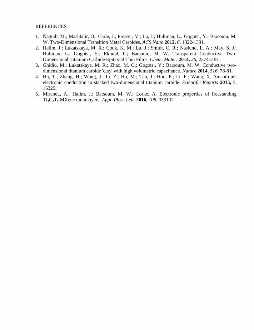
MXenes have demonstrated promise for a variety of applications and in particular for the energy storage in Li-ion,[1] Li-S,[10] Na-ion batteries,[11] and supercapacitors.[4,6] Yet, the applications of this new family of the 2D mate-rials in electronic devices, such as transistors and sensors, remain underde-veloped.[1,12–14] One of the reasons for this is the lack of experimental data on electronic properties of single- and multi-layer MXenes. Electronic proper-ties of the most widely studied MXene, Ti3C2Tx, were measured for bulk,[4,15] thin film,[3] and individual multilayer particles,[16] and—only recently—indi-vidual flakes[17] (see Table S1 in the Supporting Information for a compar-ison). However, studies of other 2D materials, such as graphene,[18] phos-phorene,[19] transition metal chalcogenides,[20] etc., have demonstrated the importance of characterizing electronic transport properties of individual monolayers and few-layer flakes. Furthermore, electronic properties of the 2D flakes strongly depend on the materials fabrication approaches and syn-thesis conditions. With little information that is currently available on the electrical properties of individual flakes of Ti3C2Tx, there is a limited under-standing of how these properties depend on the approaches used for MX-enes’ synthesis. Further electrical characterization of individual Ti3C2Tx flakes should establish the importance of the optimization of synthetic conditions for Ti3C2Tx, provide insights into its intrinsic properties, and reveal its poten-tial for relevant applications.
For electronic property studies, controlled synthesis and delamination of MXenes into large monolayer flakes of high quality is required. High-yield delamination strategies depend on the synthesis method. MXenes produced by HF etching require an additional step of intercalation with or-ganic molecules, such as DMSO[21] or amines,[22,23] whereas LiF−HCl etched MXene (also known as a “MXene clay”) can be delaminated right away by
L ipatov & Alhabeb , e t a l . in Advanced Electronic Mater ials 2 (2016 ) 4
sonication in water.[4] The purpose of this study is manifold. First, we report on the transport property measurements of monolayer Ti3C2Tx flakes. Sec-ond, we show that electronic properties and environmental stability of Ti3C2Tx flakes strongly depend on their synthesis conditions. Particular attention has been paid to the optimization of LiF−HCl etching of Ti3AlC2 to produce large high-quality MXene flakes with low concentration of defects. Finally, we demonstrate that electrical measurements can be used to study the ki-netics of environmental degradation of Ti3C2Tx flakes, which is an important issue for some of MXenes’ potential applications.
2. Results and Discussion
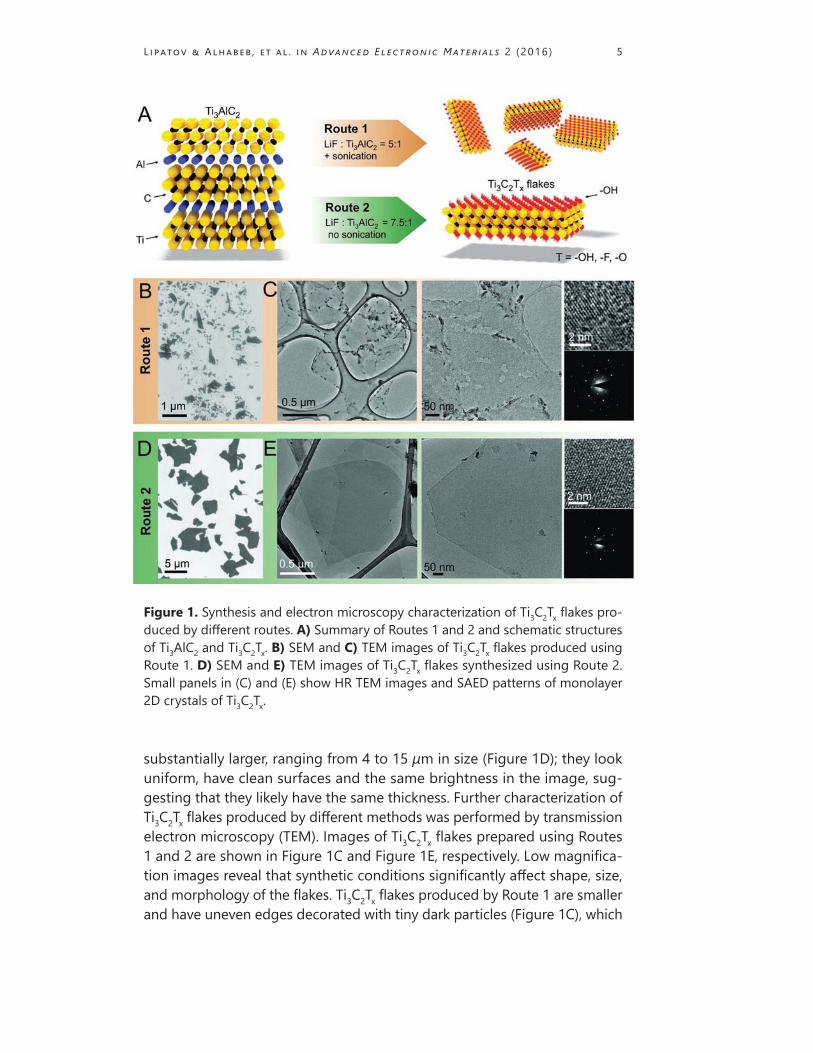
Two types of Ti3C2Tx flakes were produced for this study. Following the orig-inal procedure (Route 1) reported by Ghidiu et al.,[4] Ti3C2Tx was synthesized by immersing Ti3AlC2 powder into a LiF–HCl solution maintaining the molar ratio of LiF to MAX equal to 5:1 (see Experimental Section for details). Previ-ous studies have shown that this method yields primarily monolayer flakes.[4] In the modified procedure (Route 2), the molar ratio of LiF to MAX was in-creased to 7.5:1 to provide excess of Li+ ions for intercalation and the HCl to LiF ratio was doubled to facilitate etching of aluminum. Other aspects of the procedure remained identical, except no sonication was needed to delam-inate Ti3C2Tx particles that were produced using Route 2 (see Table 1). Key differences between Routes 1 and 2 are summarized in Figure 1A.
First, we evaluated the quality of Ti3C2Tx flakes produced by different methods by electron microscopy techniques (Figure 1B–E). Both solutions were drop-casted on silicon substrates and characterized by scanning elec-tron microscopy (SEM). The majority of the flakes produced by Route 1 are 200–500 nm in diameter (Figure 1B), and despite their small size some of the flakes are not completely exfoliated. In contrast, Route 2 MXene flakes are
Table 1. Summary of the experimental parameters for the original and modified etching/de-lamination procedures.
Original procedure, Modified procedure, Route 1 Route 2
Mass (Ti3AlC2) [g] 1 1 Mass (LiF) [g] 0.67 1Volume (6 m HCl) [mL] 10 20 Molar ratio Ti3AlC2:LiF:HCl 1.0:5.0:11.7 1.0:7.5:23.4Etching time [h] 24 24Centrifugation speed/time 3500 rpm/1 h 3500 rpm/1 hSonication Yes, 1 h No
L ipatov & Alhabeb , e t a l . in Advanced Electronic Mater ials 2 (2016 ) 5
substantially larger, ranging from 4 to 15 μm in size (Figure 1D); they look uniform, have clean surfaces and the same brightness in the image, sug-gesting that they likely have the same thickness. Further characterization of Ti3C2Tx flakes produced by different methods was performed by transmission electron microscopy (TEM). Images of Ti3C2Tx flakes prepared using Routes 1 and 2 are shown in Figure 1C and Figure 1E, respectively. Low magnifica-tion images reveal that synthetic conditions significantly affect shape, size, and morphology of the flakes. Ti3C2Tx flakes produced by Route 1 are smaller and have uneven edges decorated with tiny dark particles (Figure 1C), which
Figure 1. Synthesis and electron microscopy characterization of Ti3C2Tx flakes pro-duced by different routes. A) Summary of Routes 1 and 2 and schematic structures of Ti3AlC2 and Ti3C2Tx. B) SEM and C) TEM images of Ti3C2Tx flakes produced using Route 1. D) SEM and E) TEM images of Ti3C2Tx flakes synthesized using Route 2. Small panels in (C) and (E) show HR TEM images and SAED patterns of monolayer 2D crystals of Ti3C2Tx.
L ipatov & Alhabeb , e t a l . in Advanced Electronic Mater ials 2 (2016 ) 6
we attribute to titanium dioxide, based on the results of prior studies.[24] In high resolution TEM images, Ti3C2Tx flakes produced by Route 1 reveal nu-merous pin holes (Figure 1C). On the other hand, flakes produced using Route 2 are larger, have well-defined and clean edges and are visually hole-free (Figure 1E). Crystallographic shape of the Route 2 MXene flakes in TEM images shows that MAX phase crystals can be delaminated without break-ing the sheets. High-resolution (HR) TEM images that are presented in Fig-ure 1C,E demonstrate hexagonal arrangement of atoms, showing that the crystal structures of both flakes are identical, which was further confirmed by selected area electron diffraction (SAED) patterns. From this side-by-side comparison, it is clear that the modified synthesis procedure (Route 2) yields Ti3C2Tx flakes of visibly higher quality and larger size compared to the flakes produced using Route 1. We attribute this improvement to the change in the composition of the etching solution, which facilitated both etching of aluminum and intercalation of lithium. As a result, multilayer Ti3C2Tx flakes can be delaminated to monolayer flakes by a manual shake, with no need for sonication that shreds flakes into smaller pieces.
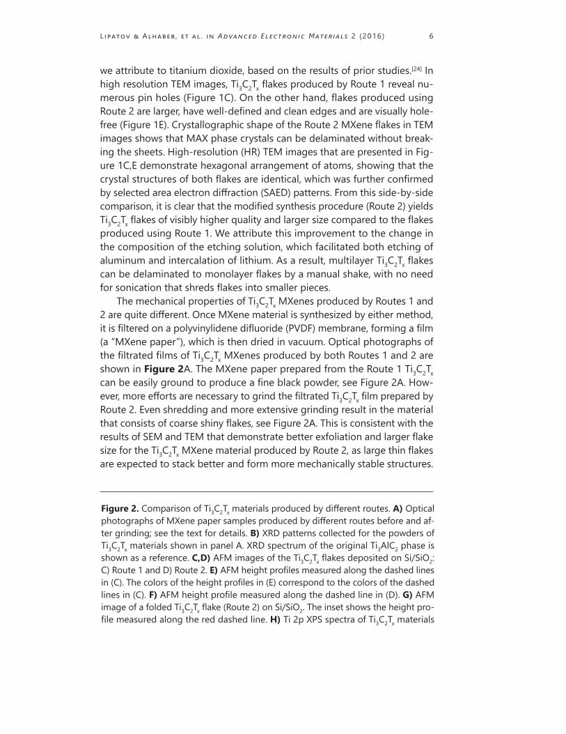
The mechanical properties of Ti3C2Tx MXenes produced by Routes 1 and 2 are quite different. Once MXene material is synthesized by either method, it is filtered on a polyvinylidene difluoride (PVDF) membrane, forming a film (a “MXene paper”), which is then dried in vacuum. Optical photographs of the filtrated films of Ti3C2Tx MXenes produced by both Routes 1 and 2 are shown in Figure 2A. The MXene paper prepared from the Route 1 Ti3C2Tx can be easily ground to produce a fine black powder, see Figure 2A. How-ever, more efforts are necessary to grind the filtrated Ti3C2Tx film prepared by Route 2. Even shredding and more extensive grinding result in the material that consists of coarse shiny flakes, see Figure 2A. This is consistent with the results of SEM and TEM that demonstrate better exfoliation and larger flake size for the Ti3C2Tx MXene material produced by Route 2, as large thin flakes are expected to stack better and form more mechanically stable structures.
Figure 2. Comparison of Ti3C2Tx materials produced by different routes. A) Optical photographs of MXene paper samples produced by different routes before and af-ter grinding; see the text for details. B) XRD patterns collected for the powders of Ti3C2Tx materials shown in panel A. XRD spectrum of the original Ti3AlC2 phase is shown as a reference. C,D) AFM images of the Ti3C2Tx flakes deposited on Si/SiO2: C) Route 1 and D) Route 2. E) AFM height profiles measured along the dashed lines in (C). The colors of the height profiles in (E) correspond to the colors of the dashed lines in (C). F) AFM height profile measured along the dashed line in (D). G) AFM image of a folded Ti3C2Tx flake (Route 2) on Si/SiO2. The inset shows the height pro-file measured along the red dashed line. H) Ti 2p XPS spectra of Ti3C2Tx materials
L ipatov & Alhabeb , e t a l . in Advanced Electronic Mater ials 2 (2016 ) 7
produced by Routes 1 and 2. Interactions of Ti with carbon and terminal atoms pro-duce three signals (blue, red, and cyan fitting curves) that are collectively marked as C-Ti-Tx 2p3/2 and C-Ti-Tx 2p1/2. These signals correspond to different oxidation states of Ti. Titanium in TiO2 produces distinctive signals at ≈459 and ≈465 eV (marked as TiO2 2p3/2 and TiO2 2p1/2).
L ipatov & Alhabeb , e t a l . in Advanced Electronic Mater ials 2 (2016 ) 8
Different stacking scenarios for the MXene flakes produced by two meth-ods are manifested in the results of powder X-ray diffraction (XRD) mea-surements. Figure 2B shows that the XRD spectrum of the Route 2 Ti3C2Tx flakes exhibits only a series of 00l reflections, indicating a layered structure of stacked flakes with an interplanar distance of 1.242 nm. In contrast, only 001 reflection is seen in the XRD pattern of the Route 1 Ti3C2Tx flakes (Fig-ure 2B), indicating that they form less ordered stacks compared to the flakes produced by Route 2. Also, this XRD pattern shows some peaks of the origi-nal MAX phase, which means that the transformation of MAX phase to MX-ene by Route 1 was not complete and some remaining incompletely exfo-liated MAX particles are still present in the sample.
The thickness and shapes of the flakes produced by both methods were investigated by atomic force microscopy (AFM), see Figure 2C–G. The com-parison of AFM images in Figure 2C and D presented at the same magnifica-tion shows that Ti3C2Tx flakes synthesized by Route 2 are significantly larger compared to the material produced by Route 1. The AFM height profile mea-sured along the blue dashed line in Figure 2D shows that all Ti3C2Tx flakes have the same height of ≈ 2.7 nm (Figure 2F) and are identified as mono-layers, as can be seen from Figure 2G that shows a folded Ti3C2Tx flake pro-duced by Route 2. The AFM height profile in the inset shows that the height of the folded region relative to the rest of the flake is ≈ 1.5 nm, which cor-responds to a single layer of Ti3C2Tx (according to DFT calculations and TEM studies, the thickness of an individual MXene flake is 0.98 nm[4,25]). However, the AFM height of the flake relative to the Si/SiO2 substrate is 2.7 nm, as in case of Figure 2D,F. The increased height is likely due to the presence of sur-face adsorbates, such as water molecules, that are trapped under the Ti3C2Tx flake; similar observations have been previously reported for other 2D ma-terials as well.[26–29] In contrast, the AFM height profiles measured along the dashed lines in Figure 2C show that the flakes produced by Route 1 have different thicknesses (Figure 2E). This observation further supports incom-plete exfoliation of MAX phase via Route 1, which is consistent with the re-sults obtained by other materials characterization methods.
The comparison of XPS spectra in the Ti 2p region for MXenes produced by Routes 1 and 2 is presented in Figure 2H. The fitting and analysis of the spectra were performed as described in previous works.[5,30,31] While the sig-nals that are marked as C-Ti-Tx 2p3/2 and C-Ti-Tx 2p1/2 [30] and correspond to Ti interactions with carbons and terminal atoms in Ti3C2Tx look similar in both spectra, there is a visible increase in the signal intensities at ≈459 and ≈465 eV (these peaks are marked as TiO2 2p3/2 and TiO2 2p1/2, respectively),[31] which is another indication of oxidation of MXenes produced via Route 1.
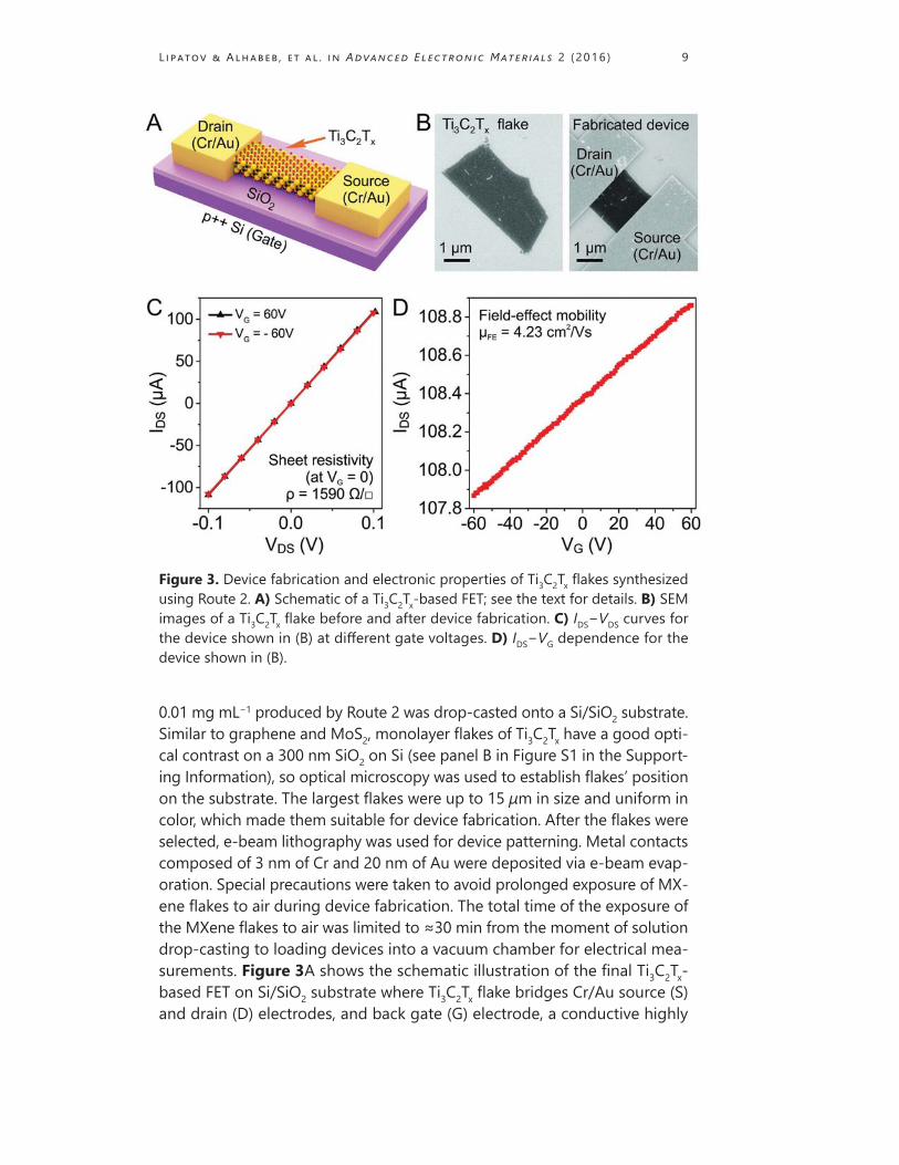
To study electronic properties of Ti3C2Tx flakes, we fabricated field-effect transistors (FETs) with individual MXene flakes as conductive channels. First, the diluted colloidal solution of Ti3C2Tx flakes with concentration of about
L ipatov & Alhabeb , e t a l . in Advanced Electronic Mater ials 2 (2016 ) 9
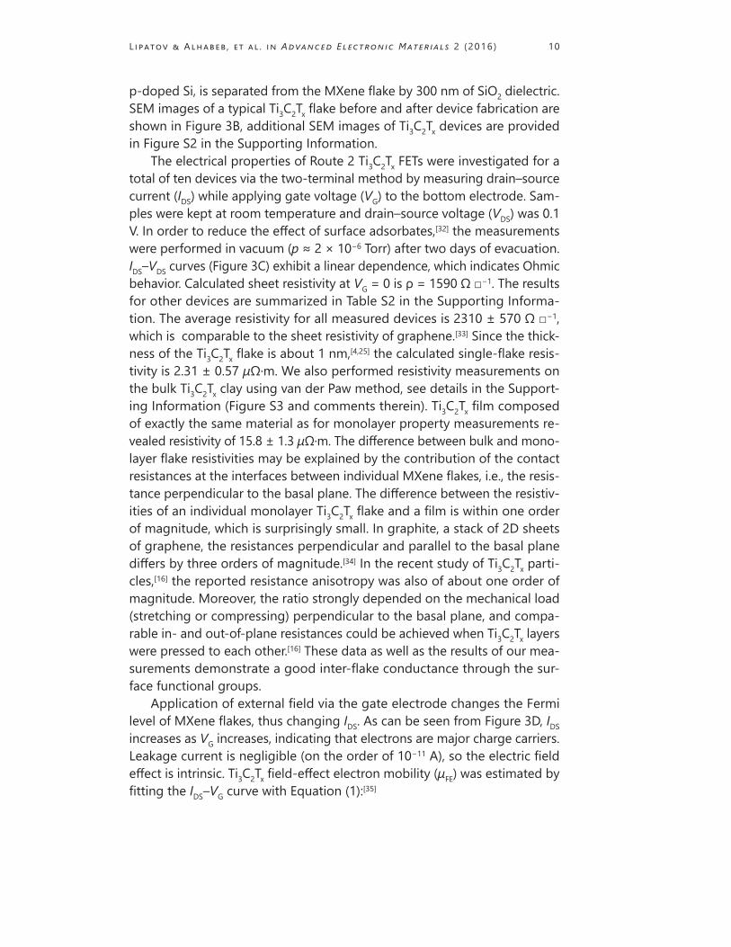
0.01 mg mL−1 produced by Route 2 was drop-casted onto a Si/SiO2 substrate. Similar to graphene and MoS2, monolayer flakes of Ti3C2Tx have a good opti-cal contrast on a 300 nm SiO2 on Si (see panel B in Figure S1 in the Support-ing Information), so optical microscopy was used to establish flakes’ position on the substrate. The largest flakes were up to 15 μm in size and uniform in color, which made them suitable for device fabrication. After the flakes were selected, e-beam lithography was used for device patterning. Metal contacts composed of 3 nm of Cr and 20 nm of Au were deposited via e-beam evap-oration. Special precautions were taken to avoid prolonged exposure of MX-ene flakes to air during device fabrication. The total time of the exposure of the MXene flakes to air was limited to ≈30 min from the moment of solution drop-casting to loading devices into a vacuum chamber for electrical mea-surements. Figure 3A shows the schematic illustration of the final Ti3C2Tx-based FET on Si/SiO2 substrate where Ti3C2Tx flake bridges Cr/Au source (S) and drain (D) electrodes, and back gate (G) electrode, a conductive highly
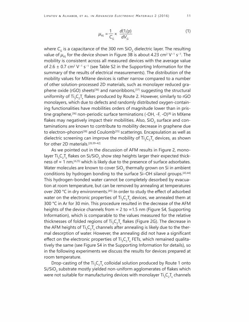
Figure 3. Device fabrication and electronic properties of Ti3C2Tx flakes synthesized using Route 2. A) Schematic of a Ti3C2Tx-based FET; see the text for details. B) SEM images of a Ti3C2Tx flake before and after device fabrication. C) IDS−VDS curves for the device shown in (B) at different gate voltages. D) IDS−VG dependence for the device shown in (B).
L ipatov & Alhabeb , e t a l . in Advanced Electronic Mater ials 2 (2016 ) 10
p-doped Si, is separated from the MXene flake by 300 nm of SiO2 dielectric. SEM images of a typical Ti3C2Tx flake before and after device fabrication are shown in Figure 3B, additional SEM images of Ti3C2Tx devices are provided in Figure S2 in the Supporting Information.
The electrical properties of Route 2 Ti3C2Tx FETs were investigated for a total of ten devices via the two-terminal method by measuring drain–source current (IDS) while applying gate voltage (VG) to the bottom electrode. Sam-ples were kept at room temperature and drain–source voltage (VDS) was 0.1 V. In order to reduce the effect of surface adsorbates,[32] the measurements were performed in vacuum (p ≈ 2 × 10⁻⁶ Torr) after two days of evacuation. IDS–VDS curves (Figure 3C) exhibit a linear dependence, which indicates Ohmic behavior. Calculated sheet resistivity at VG = 0 is ρ = 1590 Ω □−1. The results for other devices are summarized in Table S2 in the Supporting Informa-tion. The average resistivity for all measured devices is 2310 ± 570 Ω □−1, which is comparable to the sheet resistivity of graphene.[33] Since the thick-ness of the Ti3C2Tx flake is about 1 nm,[4,25] the calculated single-flake resis-tivity is 2.31 ± 0.57 μΩ·m. We also performed resistivity measurements on the bulk Ti3C2Tx clay using van der Paw method, see details in the Support-ing Information (Figure S3 and comments therein). Ti3C2Tx film composed of exactly the same material as for monolayer property measurements re-vealed resistivity of 15.8 ± 1.3 μΩ·m. The difference between bulk and mono-layer flake resistivities may be explained by the contribution of the contact resistances at the interfaces between individual MXene flakes, i.e., the resis-tance perpendicular to the basal plane. The difference between the resistiv-ities of an individual monolayer Ti3C2Tx flake and a film is within one order of magnitude, which is surprisingly small. In graphite, a stack of 2D sheets of graphene, the resistances perpendicular and parallel to the basal plane differs by three orders of magnitude.[34] In the recent study of Ti3C2Tx parti-cles,[16] the reported resistance anisotropy was also of about one order of magnitude. Moreover, the ratio strongly depended on the mechanical load (stretching or compressing) perpendicular to the basal plane, and compa-rable in- and out-of-plane resistances could be achieved when Ti3C2Tx layers were pressed to each other.[16] These data as well as the results of our mea-surements demonstrate a good inter-flake conductance through the sur-face functional groups.
Application of external field via the gate electrode changes the Fermi level of MXene flakes, thus changing IDS. As can be seen from Figure 3D, IDS increases as VG increases, indicating that electrons are major charge carriers. Leakage current is negligible (on the order of 10−11 A), so the electric field effect is intrinsic. Ti3C2Tx field-effect electron mobility (μFE) was estimated by fitting the IDS–VG curve with Equation (1):[35]
L ipatov & Alhabeb , e t a l . in Advanced Electronic Mater ials 2 (2016 ) 11
μFE = 1 × d(1/ρ) (1)
CG dVG
where CG is a capacitance of the 300 nm SiO2 dielectric layer. The resulting value of μFE for the device shown in Figure 3B is about 4.23 cm2 V−1 s−1. The mobility is consistent across all measured devices with the average value of 2.6 ± 0.7 cm2 V−1 s−1 (see Table S2 in the Supporting Information for the summary of the results of electrical measurements). The distribution of the mobility values for MXene devices is rather narrow compared to a number of other solution-processed 2D materials, such as monolayer reduced gra-phene oxide (rGO) sheets[36] and nanoribbons,[37] suggesting the structural uniformity of Ti3C2Tx flakes produced by Route 2. However, similarly to rGO monolayers, which due to defects and randomly distributed oxygen-contain-ing functionalities have mobilities orders of magnitude lower than in pris-tine graphene,[36] non-periodic surface terminations (-OH, -F, -O)[8] in MXene flakes may negatively impact their mobilities. Also, SiO2 surface and con-taminations are known to contribute to mobility decrease in graphene due to electron–phonon[38] and Coulomb[35] scatterings. Encapsulation as well as dielectric screening can improve the mobility of Ti3C2Tx devices, as shown for other 2D materials.[20,39–42]
As we pointed out in the discussion of AFM results in Figure 2, mono-layer Ti3C2Tx flakes on Si/SiO2 show step heights larger their expected thick-ness of ≈ 1 nm,[4,25] which is likely due to the presence of surface adsorbates. Water molecules are known to cover SiO2 thermally grown on Si in ambient conditions by hydrogen bonding to the surface Si–OH silanol groups.[43,44] This hydrogen-bonded water cannot be completely desorbed by evacua-tion at room temperature, but can be removed by annealing at temperatures over 200 °C in dry environments.[45] In order to study the effect of adsorbed water on the electronic properties of Ti3C2Tx devices, we annealed them at 300 °C in Ar for 30 min. This procedure resulted in the decrease of the AFM heights of the device channels from ≈ 2 to ≈1.5 nm (Figure S4, Supporting Information), which is comparable to the values measured for the relative thicknesses of folded regions of Ti3C2Tx flakes (Figure 2G). The decrease in the AFM heights of Ti3C2Tx channels after annealing is likely due to the ther-mal desorption of water. However, the annealing did not have a significant effect on the electronic properties of Ti3C2Tx FETs, which remained qualita-tively the same (see Figure S4 in the Supporting Information for details), so in the following experiments we discuss the results for devices prepared at room temperature.
Drop-casting of the Ti3C2Tx colloidal solution produced by Route 1 onto Si/SiO2 substrate mostly yielded non-uniform agglomerates of flakes which were not suitable for manufacturing devices with monolayer Ti3C2Tx channels
L ipatov & Alhabeb , e t a l . in Advanced Electronic Mater ials 2 (2016 ) 12
(see panel A in Figure S1 in the Supporting Information). Occasionally, small (< 5 μm) flakes could be spotted. FETs with Ti3C2Tx flakes produced by Route 1 were fabricated using the same procedure as for the Route 2 flakes, and representative SEM images of the devices are shown in Figure S5 in the Supporting Information. The devices were not conductive, and we explain this results by a higher oxidation degree of the Route 1 flakes compared to the Route 2 ones (Figure 2H), and their lower environmental stability due to numerous pin-hole defects (Figure 1 C), which facilitate oxidation of MX-ene flakes in air. These results, demonstrate the importance of the synthe-sis procedure for high-quality and environmentally stable MXene flakes for electronic applications.
Monolayer MXene flakes cannot sustain prolonged exposure to oxy-gen in the presence of water[24] or at high temperature.[46] Previous studies showed the formation of titanium dioxide and carbon, with nucleation of ti-tania crystals along the edges of MXene flakes.[46] For instance, when colloi-dal solution of delaminated MXene in water is exposed to air, Ti3C2Tx flakes are completely oxidized within several days. This results in the solution color change from translucent black/brown to cloudy white, with a white precip-itate of titania accumulating at the bottom of a vial. In this work, we stud-ied kinetics of the environmental degradation of an individual Ti3C2Tx flake in situ by measuring the change of FETs’ conductivity in air as a function of time. Device measurements have been previously used to study kinetics of other reactions involving 2D materials, such as diazonium functionalization of graphene.[47]
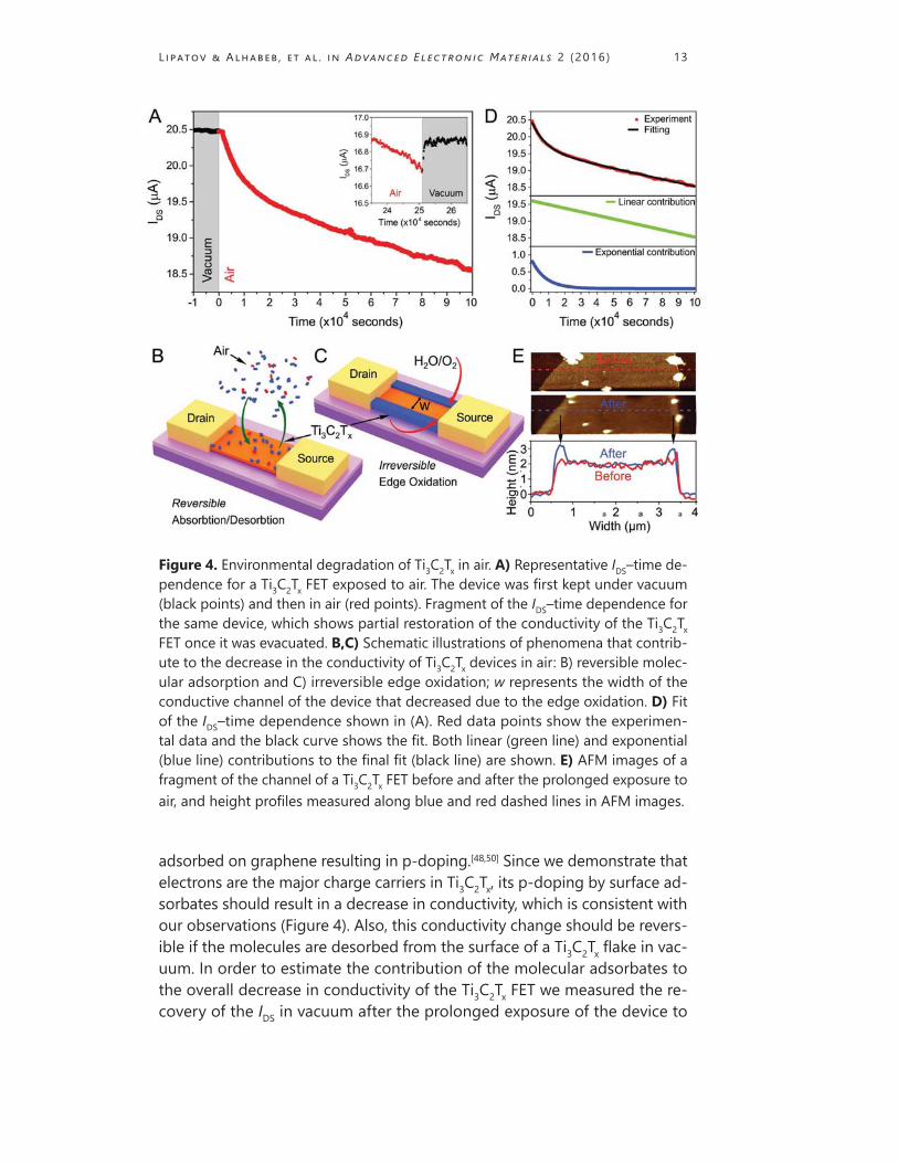
In these measurements we monitored the IDS every 10 s, while exposing one of the previously discussed Ti3C2Tx devices to air at room temperature and relative humidity of ≈50%. Figure 4A shows the resulting time-depen-dence of IDS. Black points at time (t) < 0 correspond to the readings in vac-uum before the device was exposed to air. The readings were stable in vac-uum but once the lid of a vacuum chamber was opened, the drain–source current started to decrease (see red data points in Figure 4A). The data were collected for 2.5 × 10⁵ s (≈ 70 h) during which the IDS decreased from 20.5 to 16.7 μA. The IDS first decayed strongly in a non-linear manner within the ini-tial ≈2 × 10⁴ s, however, later, IDS exhibited a linear decay over time. It should also be noted that linear dependence of IDS–VDS curves was preserved af-ter the device was kept in air for 70 h, which indicates the degradation of Ti3C2Tx flake rather than contacts between the flake and metal electrodes.
The observed decrease in the conductivity of a Ti3C2Tx flake represents in-terplay of several different effects. First of all, we consider molecular adsorp-tion on Ti3C2Tx flakes (Figure 4B). It was previously shown that surface adsor-bates may cause doping of 2D materials, such as graphene.[32,48,49] In case of air, particularly important adsorbates are oxygen and water molecules, both of which have been demonstrated to behave as electron acceptors when
L ipatov & Alhabeb , e t a l . in Advanced Electronic Mater ials 2 (2016 ) 13
adsorbed on graphene resulting in p-doping.[48,50] Since we demonstrate that electrons are the major charge carriers in Ti3C2Tx, its p-doping by surface ad-sorbates should result in a decrease in conductivity, which is consistent with our observations (Figure 4). Also, this conductivity change should be revers-ible if the molecules are desorbed from the surface of a Ti3C2Tx flake in vac-uum. In order to estimate the contribution of the molecular adsorbates to the overall decrease in conductivity of the Ti3C2Tx FET we measured the re-covery of the IDS in vacuum after the prolonged exposure of the device to
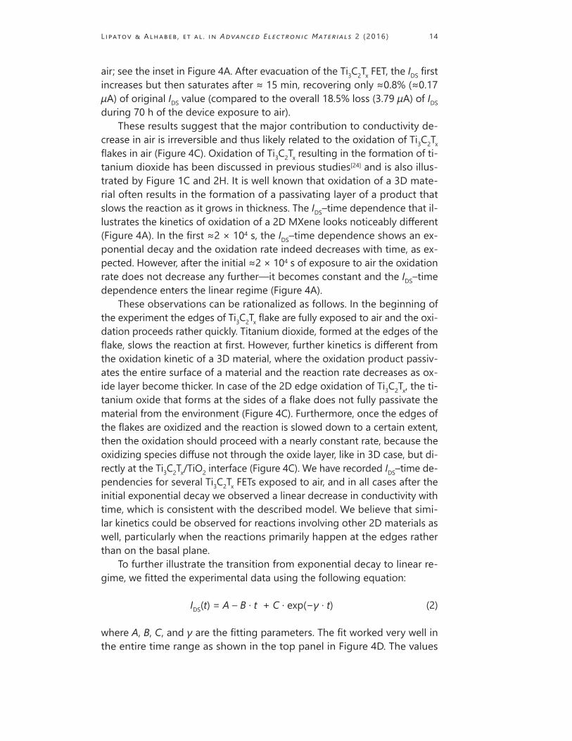
Figure 4. Environmental degradation of Ti3C2Tx in air. A) Representative IDS–time de-pendence for a Ti3C2Tx FET exposed to air. The device was first kept under vacuum (black points) and then in air (red points). Fragment of the IDS–time dependence for the same device, which shows partial restoration of the conductivity of the Ti3C2Tx FET once it was evacuated. B,C) Schematic illustrations of phenomena that contrib-ute to the decrease in the conductivity of Ti3C2Tx devices in air: B) reversible molec-ular adsorption and C) irreversible edge oxidation; w represents the width of the conductive channel of the device that decreased due to the edge oxidation. D) Fit of the IDS–time dependence shown in (A). Red data points show the experimen-tal data and the black curve shows the fit. Both linear (green line) and exponential (blue line) contributions to the final fit (black line) are shown. E) AFM images of a fragment of the channel of a Ti3C2Tx FET before and after the prolonged exposure to air, and height profiles measured along blue and red dashed lines in AFM images.
L ipatov & Alhabeb , e t a l . in Advanced Electronic Mater ials 2 (2016 ) 14
air; see the inset in Figure 4A. After evacuation of the Ti3C2Tx FET, the IDS first increases but then saturates after ≈ 15 min, recovering only ≈0.8% (≈0.17 μA) of original IDS value (compared to the overall 18.5% loss (3.79 μA) of IDS during 70 h of the device exposure to air).
These results suggest that the major contribution to conductivity de-crease in air is irreversible and thus likely related to the oxidation of Ti3C2Tx flakes in air (Figure 4C). Oxidation of Ti3C2Tx resulting in the formation of ti-tanium dioxide has been discussed in previous studies[24] and is also illus-trated by Figure 1C and 2H. It is well known that oxidation of a 3D mate-rial often results in the formation of a passivating layer of a product that slows the reaction as it grows in thickness. The IDS–time dependence that il-lustrates the kinetics of oxidation of a 2D MXene looks noticeably different (Figure 4A). In the first ≈2 × 10⁴ s, the IDS–time dependence shows an ex-ponential decay and the oxidation rate indeed decreases with time, as ex-pected. However, after the initial ≈2 × 10⁴ s of exposure to air the oxidation rate does not decrease any further—it becomes constant and the IDS–time dependence enters the linear regime (Figure 4A).
These observations can be rationalized as follows. In the beginning of the experiment the edges of Ti3C2Tx flake are fully exposed to air and the oxi-dation proceeds rather quickly. Titanium dioxide, formed at the edges of the flake, slows the reaction at first. However, further kinetics is different from the oxidation kinetic of a 3D material, where the oxidation product passiv-ates the entire surface of a material and the reaction rate decreases as ox-ide layer become thicker. In case of the 2D edge oxidation of Ti3C2Tx, the ti-tanium oxide that forms at the sides of a flake does not fully passivate the material from the environment (Figure 4C). Furthermore, once the edges of the flakes are oxidized and the reaction is slowed down to a certain extent, then the oxidation should proceed with a nearly constant rate, because the oxidizing species diffuse not through the oxide layer, like in 3D case, but di-rectly at the Ti3C2Tx/TiO2 interface (Figure 4C). We have recorded IDS–time de-pendencies for several Ti3C2Tx FETs exposed to air, and in all cases after the initial exponential decay we observed a linear decrease in conductivity with time, which is consistent with the described model. We believe that simi-lar kinetics could be observed for reactions involving other 2D materials as well, particularly when the reactions primarily happen at the edges rather than on the basal plane.
To further illustrate the transition from exponential decay to linear re-gime, we fitted the experimental data using the following equation:
IDS(t) = A – B ∙ t + C ∙ exp(−γ ∙ t) (2)
where A, B, C, and γ are the fitting parameters. The fit worked very well in the entire time range as shown in the top panel in Figure 4D. The values
L ipatov & Alhabeb , e t a l . in Advanced Electronic Mater ials 2 (2016 ) 15
extracted by fitting the experimental data with Equation (2) are A = 19.599(2) A, B = 1.068(3) × 10−5 A s−1, C = 0.810(3) A, and γ = 1.16(1)×10−4 s−1. The middle and bottom panels in Figure 4D demonstrate individual contribu-tions of linear and exponential parts of Equation (2). They further demon-strate that the exponential term initially dominates, but then the contribu-tion of the linear term becomes more important.
Edges of Ti3C2Tx flakes and other structural defects (Ti vacancies and pin holes) are the most vulnerable sites for oxidation. For the Ti3C2Tx flakes with high structural quality (prepared by Route 2), it is reasonable to assume that the edge oxidation will proceed faster than the oxidation at the basal plane and thus will make the largest contribution to the overall conductivity de-crease. This scenario is illustrated by Figure 4C that shows that the edge ox-idation decreases the width of the Ti3C2Tx FET channel (w), which results in the conductivity decrease. To verify this assumption, we compared AFM im-ages of as-prepared Ti3C2Tx FETs with AFM images of the same device after prolonged exposure to air. Figure 4E shows that the Ti3C2Tx channel of as-prepared device has a uniform thickness of ≈ 2 nm. After exposure to air the flake becomes visibly thicker at the edges, but the thickness does not change at the basal plane. This observation is consistent with the assumption that the environmental degradation primarily happens at the exposed edges of the Ti3C2Tx flake, while the basal plane is reasonably inert to oxidation. The height profiles measured along the same portion of the Ti3C2Tx channel be-fore and after exposure to air for 70 h show that the flake thickness increases at the edges by ≈ 1 nm (see arrows in Figure 4E). The AFM data confirm the conclusion made from the results of electrical measurements that environ-mental degradation of high-quality Ti3C2Tx flakes is reasonably slow. Since the oxidized edges are less conductive than the interiors of Ti3C2Tx flakes, they could be visualized by scanning electron microscopy. SEM images of Ti3C2Tx flakes that were deposited on Si/SiO2 substrates and exposed to air for several days show that the edges of flakes are visibly brighter than their interiors (Figure S6, Supporting Information)—such contrast was not ob-served for the Ti3C2Tx flakes that were imaged shortly after their deposition on Si/ SiO2 substrates, see Figure 1B,D.
The sensitivity of the conductivity of Ti3C2Tx to molecular adsorbates and some reversibility of the process suggest the potential of this mate-rial and other MXenes for sensor applications. Previously, different kinds of sensors were demonstrated for many other 2D materials, such as gra-phene, graphene oxide, and transition metal chalcogenides; which benefit from high surface-to-volume ratios and tunable electronic properties.[51,52] Very rich surface chemistry of MXenes with about 20 compositions of var-ious transition metals and their combinations available to date[53,54] makes MXene FETs promising for sensing applications as well. Of course, the envi-ronmental degradation could be a serious issue for such sensors. However,
L ipatov & Alhabeb , e t a l . in Advanced Electronic Mater ials 2 (2016 ) 16
considering that the oxidation of high-quality Ti3C2Tx flakes primarily hap-pens at the edges, this issue could be mitigated by passivating edges with inert oxide materials using, for example, a technique like atomic layer depo-sition, or encapsulating them with impermeable 2D materials, such as hex-agonal boron nitride (h-BN).
3. Conclusions
In summary, we demonstrate an improved method of selective etching of Ti3AlC2, a MAX phase, which yields large high-quality monolayer Ti3C2Tx MX-ene flakes with well-defined and clean edges and visually defect-free sur-faces. We fabricated FETs based on monolayer Ti3C2Tx flakes, which exhibited a field-effect electron mobility of 2.6 ± 0.7 cm2 V−1 s−1 and a low resistiv-ity of 2.31 ± 0.57 μΩ·m (4600 ± 1100 S cm−1). The single flake resistivity is only one order of magnitude higher than the resistivity of bulk Ti3C2Tx and thin films made from Ti3C2Tx flakes, suggesting that Ti3C2Tx flakes form low-resistance electric contacts with each other, which is a practically important result for bulk applications of this material. Finally, we used fabricated FETs to investigate the environmental stability of Ti3C2Tx flakes in humid air. The high-quality Ti3C2Tx flakes are reasonably stable and remain highly conduc-tive even after their exposure to air for 70 h. After the initial exponential de-cay the drain–source current linearly decreases with time. We explain these observations by the edge oxidation of Ti3C2Tx flakes and support this expla-nation by AFM measurements. We believe that similar kinetics could be ob-served for reactions involving other 2D materials as well, in cases when the reactions primarily happen at the edges. Many of such kinetics studies of other conductive 2D materials may potentially be carried out using the elec-trical measurement scheme that was disclosed in this paper.
4. Experimental Section
Synthesis of Ti3C2Tx Following the Original[4] and Modified Procedure: MAX phase precursor, Ti3AlC2, was produced as described elsewhere.[4] Following the procedure reported by Ghidiu et al.,[4] 0.67 g of LiF was dissolved in 10 mL of 6 m HCl and the solution was allowed to mix thoroughly at room tem-perature for a few minutes. After that, 1 g of Ti3AlC2 was slowly added over the course of 5 min to avoid initial overheating due to exothermic nature of the reaction. Then, the temperature was brought to 35 °C and the reaction allowed to proceed under continuous stirring (550 rpm) for 24 h. The result-ing MXene powder was repeatedly washed with DI water until almost neutral pH (≥ 6). The product was then collected using vacuum-assisted filtration
L ipatov & Alhabeb , e t a l . in Advanced Electronic Mater ials 2 (2016 ) 17
through a PVDF membrane (0.45 μm pore size, Millipore) and dried in a vac-uum desiccator at room temperature for 24 h. To delaminate 0.2 g of Ti3C2Tx, the freshly produced powder was bath sonicated in 50 mL of DI water for 1 h under continuous argon (Ar) bubbling to minimize oxidation. Then, the Ti3C2Tx solution was centrifuged at 3500 rpm for 1 h and the supernatant, a colloidal solution of MXene, was collected. Previous studies have shown that this solution contains primarily monolayer flakes.[4] In the modified proce-dure, 1 g of MAX was added to the mixture of 1 g of LiF in 20 mL of 6 m HCl. Other aspects of the procedure remained identical except that the delam-ination of the resulting Ti3C2Tx powder did not require sonication (Table 1).
Supporting Information follows the References.
Acknowledgments — Alexey Lipatov and Mohamed Alhabeb contributed equally to this work. All the authors have given approval to the final version of the manu-script. This work was supported by the National Science Foundation (NSF) through ECCS-1509874 with a partial support from the Nebraska Materials Research Sci-ence and Engineering Center (MRSEC) (grant no. DMR-1420645). Materials synthe-sis at Drexel University was supported by the Fluid Interface Reactions, Structures and Transport (FIRST) Center, the Energy Frontier Research Center funded by the U.S. Department of Energy, Office of Science, Office of Basic Energy Sciences. The authors thank Patrick Urbankowski for the XPS characterization of MXene flakes. The authors declare no competing financial interests.
References
[1] M. Naguib, V. N. Mochalin, M. W. Barsoum, Y. Gogotsi, Adv. Mater. 2014, 26, 992, [2] M. Naguib, M. Kurtoglu, V. Presser, J. Lu, J. J. Niu, M. Heon, L. Hultman, Y. Gogotsi,
M. W. Barsoum, Adv. Mater. 2011, 23, 4248. [3] J. Halim, M. R. Lukatskaya, K. M. Cook, J. Lu, C. R. Smith, L. A. Naslund, S. J. May,
L. Hultman, Y. Gogotsi, P. Eklund, M. W. Barsoum, Chem. Mater. 2014, 26, 2374. [4] M. Ghidiu, M. R. Lukatskaya, M. Q. Zhao, Y. Gogotsi, M. W. Barsoum, Nature
2014, 516, 78. [5] J. Halim, K. M. Cook, M. Naguib, P. Eklund, Y. Gogotsi, J. Rosen, M. W. Barsoum,
Appl. Surf. Sci. 2015, 362, 406. [6] M. R. Lukatskaya, O. Mashtalir, C. E. Ren, Y. Dall’Agnese, P. Rozier, P. L. Taberna, M.
Naguib, P. Simon, M. W. Barsoum, Y. Gogotsi, Science 2013, 341, 1502. [7] Y. Dall’Agnese, M. R. Lukatskaya, K. M. Cook, P. L. Taberna, Y. Gogotsi, P. Simon,
Electrochem. Commun. 2014, 48, 118. [8] H.-W. Wang, M. Naguib, K. Page, D. J. Wesolowski, Y. Gogotsi, Chem. Mater. 2016,
28, 349. [9] M. A. Hope, A. C. Forse, K. J. Griffith, M. R. Lukatskaya, M. Ghidiu, Y. Gogotsi, C.
P. Grey, Phys. Chem. Chem. Phys. 2016, 18, 5099. [10] X. Liang, A. Garsuch, L. F. Nazar, Angew. Chem. Int. Ed. 2015, 54, 3907.
L ipatov & Alhabeb , e t a l . in Advanced Electronic Mater ials 2 (2016 ) 18
[11] X. Wang, S. Kajiyama, H. Iinuma, E. Hosono, S. Oro, I. Moriguchi, M. Okubo, A. Yamada, Nat. Commun. 2015, 6, 6544.
[12] J. Chen, K. Chen, D. Tong, Y. Huang, J. Zhang, J. Xue, Q. Huang, T. Chen, Chem. Commun. 2015, 51, 314.
[13] S. Lai, J. Jeon, S. K. Jang, J. Xu, Y. J. Choi, J.-H. Park, E. Hwang, S. Lee, Nanoscale 2015, 7, 19390.
[14] C. Xu, L. Wang, Z. Liu, L. Chen, J. Guo, N. Kang, X.-L. Ma, H.-M. Cheng, W. Ren, Nat. Mater. 2015, 14, 1135.
[15] M. Naguib, O. Mashtalir, J. Carle, V. Presser, J. Lu, L. Hultman, Y. Gogotsi, M. W. Barsoum, ACS Nano 2012, 6, 1322.
[16] T. Hu, H. Zhang, J. Wang, Z. Li, M. Hu, J. Tan, P. Hou, F. Li, X. Wang, Sci. Rep. 2015, 5, 16329.
[17] A. Miranda, J. Halim, M. W. Barsoum, A. Lorke, Appl. Phys. Lett. 2016, 108, 033102.
[18] K. S. Novoselov, A. K. Geim, S. V. Morozov, D. Jiang, Y. Zhang, S. V. Dubonos, I. V. Grigorieva, A. A. Firsov, Science 2004, 306, 666.
[19] H. Liu, A. T. Neal, Z. Zhu, Z. Luo, X. Xu, D. Tomanek, P. D. Ye, ACS Nano 2014, 8, 4033.
[20] B. Radisavljevic, A. Radenovic, J. Brivio, V. Giacometti, A. Kis, Nat. Nanotechnol. 2011, 6, 147.
[21] O. Mashtalir, M. Naguib, V. N. Mochalin, Y. Dall’Agnese, M. Heon, M. W. Bar-soum, Y. Gogotsi, Nat. Commun. 2013, 4, 1716.
[22] O. Mashtalir, M. R. Lukatskaya, M. Q. Zhao, M. W. Barsoum, Y. Gogotsi, Adv. Ma-ter. 2015, 27, 3501.
[23] M. Naguib, R. R. Unocic, B. L. Armstrong, J. Nanda, Dalton Trans. 2015, 44, 9353. [24] O. Mashtalir, K. M. Cook, V. N. Mochalin, M. Crowe, M. W. Barsoum, Y. Gogotsi,
J. Mater. Chem. A 2014, 2, 14334. [25] X. Wang, X. Shen, Y. Gao, Z. Wang, R. Yu, L. Chen, J. Am. Chem. Soc. 2015, 137,
2715. [26] K. S. Novoselov, D. Jiang, F. Schedin, T. J. Booth, V. V. Khotkevich, S. V. Morozov,
A. K. Geim, Proc. Natl. Acad. Sci. USA 2005, 102, 10451. [27] K. Xu, P. Cao, J. R. Heath, Science 2010, 329, 1188. [28] O. Ochedowski, B. K. Bussmann, M. Schleberger, Sci. Rep. 2014, 4, 6003. [29] H. Coy Diaz, R. Addou, M. Batzill, Nanoscale 2014, 6, 1071. [30] C. E. Ren, M.-Q. Zhao, T. Makaryan, J. Halim, M. Boota, S. Kota, B. Anasori, M. W.
Barsoum, Y. Gogotsi, ChemElectroChem 2016, 3, 689. [31] Z. Song, J. Hrbek, R. Osgood, Nano Lett. 2005, 5, 1327. [32] A. Sinitskii, A. Dimiev, D. V. Kosynkin, J. M. Tour, ACS Nano 2010, 4, 5405. [33] A. Lipatov, B. B. Wymore, A. Fursina, T. H. Vo, A. Sinitskii, J. G. Redepenning,
Chem. Mat. 2015, 27, 157. [34] H. O. Pierson, in Handbook of Carbon, Graphite, Diamonds and Fullerenes (Ed:
H. O. Pierson), William Andrew Publishing, Oxford, 1993, p. 43.
L ipatov & Alhabeb , e t a l . in Advanced Electronic Mater ials 2 (2016 ) 19
[35] J. H. Chen, C. Jang, S. Adam, M. S. Fuhrer, E. D. Williams, M. Ishigami, Nat. Phys. 2008, 4, 377.
[36] C. Gomez-Navarro, R. T. Weitz, A. M. Bittner, M. Scolari, A. Mews, M. Burghard, K. Kern, Nano Lett. 2007, 7, 3499.
[37] A. Sinitskii, A. A. Fursina, D. V. Kosynkin, A. L. Higginbotham, D. Natelson, J. M. Tour, Appl. Phys. Lett. 2009, 95, 253108.
[38] D. K. Efetov, P. Kim, Phys. Rev. Lett. 2010, 105, 256805. [39] C. R. Dean, A. F. Young, I. Meric, C. Lee, L. Wang, S. Sorgenfrei, K. Watanabe, T.
Taniguchi, P. Kim, K. L. Shepard, J. Hone, Nat. Nano 2010, 5, 722. [40] F. Chen, J. Xia, D. K. Ferry, N. Tao, Nano Lett. 2009, 9, 2571. [41] C. Jang, S. Adam, J. H. Chen, E. D. Williams, S. Das Sarma, M. S. Fuhrer, Phys. Rev.
Lett. 2008, 101, 146805. [42] A. Lipatov, P. M. Wilson, M. Shekhirev, J. D. Teeter, R. Netusil, A. Sinitskii, Na-
noscale 2015, 7, 12291. [43] D. B. Asay, S. H. Kim, J. Phys. Chem. B 2005, 109, 16760. [44] A. Verdaguer, C. Weis, G. Oncins, G. Ketteler, H. Bluhm, M. Salmeron, Langmuir
2007, 23, 9699. [45] L. T. Zhuravlev, Colloids Surf. A: Physicochem. Eng. Aspects 2000, 173, 1. [46] H. Ghassemi, W. Harlow, O. Mashtalir, M. Beidaghi, M. R. Lukatskaya, Y. Gogotsi,
M. L. Taheri, J. Mater. Chem. A 2014, 2, 14339. [47] A. Sinitskii, A. Dimiev, D. A. Corley, A. A. Fursina, D. V. Kosynkin, J. M. Tour, ACS
Nano 2010, 4, 1949. [48] F. Schedin, A. K. Geim, S. V. Morozov, E. W. Hill, P. Blake, M. I. Katsnelson, K. S.
Novoselov, Nat. Mater. 2007, 6, 652. [49] H. Liu, Y. Liu, D. Zhu, J. Mater. Chem. 2011, 21, 3335. [50] Y. Sato, K. Takai, T. Enoki, Nano Lett. 2011, 11, 3468. [51] A. Lipatov, A. Varezhnikov, P. Wilson, V. Sysoev, A. Kolmakov, A. Sinitskii, Na-
noscale 2013, 5, 5426. [52] A. Lipatov, A. Varezhnikov, M. Augustin, M. Bruns, M. Sommer, V. Sysoev, A. Kol-
makov, A. Sinitskii, Appl. Phys. Lett. 2014, 104, 013114. [53] M. Naguib, Y. Gogotsi, Acc. Chem. Res. 2015, 48, 128. [54] B. Anasori, Y. Xie, M. Beidaghi, J. Lu, B. C. Hosler, L. Hultman, P. R. C. Kent, Y.
Gogotsi, M. W. Barsoum, ACS Nano 2015, 9, 9507.
Supporting Information
Effect of synthesis on quality, electronic properties
and environmental stability of individual Ti3C2
MXene flakes
Alexey Lipatov,a, Mohamed Alhabeb,b,c Maria R. Lukatskaya,b,c Alex Boson,a Yury Gogotsi, b,c,*
Alexander Sinitskiia,d,*
a Department of Chemistry, University of Nebraska – Lincoln, Lincoln, NE 68588, USA
b Department of Materials Science and Engineering, Drexel University, Philadelphia, PA 19104, USA
c A.J. Drexel Nanomaterials Institute, Drexel University, Philadelphia, PA 19104, USA
d Nebraska Center for Materials and Nanoscience, University of Nebraska – Lincoln, Lincoln, NE 68588, USA
Corresponding Author
*E-mail: [email protected] (Y.G.), [email protected] (A.S.)
EXPERIMENTAL PROCEDURES
Materials. P-type silicon wafers covered with 300 ± 15 nm thick SiO2 (Silicon Quest International)
were used as substrates for device fabrication. Lithium fluoride (Alfa Aesar, 98.5%) and
concentrated hydrochloric acid (Fisher Scientific, 37.2%) were used as received for MXene
synthesis. PMMA950 A4 (4% polymethyl methacrylate in anisole, MicroChem Corp.), methyl
isobutyl ketone : isopropanol (1:3) (MIBK:IPA, MicroChem Corp.), isopropanol (IPA, Sigma-
Aldrich, 99.5+% ), and acetone (Fisher Scientific, 99.7%) were used as received for electron beam
lithography to pattern the electrodes on MXene flakes. Chromium (Cr, 99.995%) and gold (Au,
99.999%) targets were purchased from International Advanced Materials and used for electron beam
evaporation.
Device Fabrication. PMMA was spin-coated on a Si/SiO2 substrate with Ti3C2Tx flakes at 5000 rpm
for 45 s. Then the substrate was placed on a hotplate at 180 °C for 120 s. A Zeiss Supra 40 Field-
Emission Scanning Electron Microscope and a Raith Pattern Generator were used for electron beam
lithography to pattern electrodes on a Ti3C2Tx flake. After exposure, the substrate was developed in
the MIBK:IPA mixture for 60 s, then successively rinsed with 2-propanol and DI water, and dried
with nitrogen gas. An AJA electron beam evaporation system at the base pressure of ~8×10⁻⁹
Torr
was used to evaporate 3 nm of Cr at 0.1 Å/s rate, which as monitored using a quartz crystal
microbalance. This was immediately followed by evaporation of 20 nm of Au at 0.2 Å/s rate.
PMMA and excessive metals were removed by lift-off in acetone for 10 min. Finally, the substrate
was rinsed with isopropanol and water, and dried with nitrogen gas.
Characterization of MXene Flakes
Scanning Electron Microscopy (SEM). SEM analysis was performed using a Zeiss Supra 40 Field-
Emission Scanning Electron Microscope at the accelerating voltage of 5 kV.
Atomic Force Microscopy (AFM). All AFM images were collected in a contact and tapping modes
using a Digital Instruments Nanoscope IIIa Dimension 3100 scanning probe microscope. The AFM
data were analyzed using Nanoscope Analysis software.
Transmission Electron Microscopy (TEM). The microstructure of Ti3C2Tx flakes was studied using
a FEI Tecnai Osiris scanning transmission electron microscope equipped with a HAADF detector
and an X-FEG high brightness Schottky field emission gun. The accelerating voltage was 200 kV.
X-ray Diffraction (XRD). X-ray intensity data was collected on a Rigaku Smart lab (Tokyo, Japan)
diffractometer with Cu Kα radiation ( = 0.15418 nm) operated at 40 kV and 30 mA; step scan 0.02°,
2θ range 3°-70°, step time 0.6s. All samples were loaded and flattened over a glass sample holder
that has depth of 2 mm and an area of 2 cm2.
Device Characterization. Electrical measurements were performed using a Lake Shore TTPX
cryogenic probe station at the base pressure of 2×10⁻⁶
Torr. The device electrodes were connected
to an Agilent 4155C semiconductor parameter analyzer that was linked to a computer through
82357B USB/GPIB interface and controlled using a National Instruments LabView code.
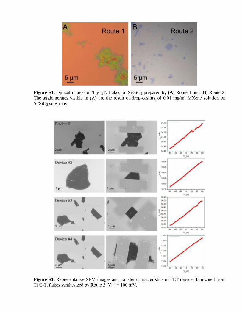
Figure S1. Optical images of Ti3C2Tx flakes on Si/SiO2 prepared by (A) Route 1 and (B) Route 2.
The agglomerates visible in (A) are the result of drop-casting of 0.01 mg/ml MXene solution on
Si/SiO2 substrate.
Figure S2. Representative SEM images and transfer characteristics of FET devices fabricated from
Ti3C2Tx flakes synthesized by Route 2. VDS = 100 mV.
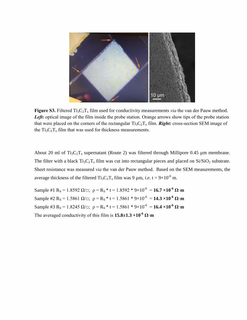
Figure S3. Filtered Ti3C2Tx film used for conductivity measurements via the van der Pauw method.
Left: optical image of the film inside the probe station. Orange arrows show tips of the probe station
that were placed on the corners of the rectangular Ti3C2Tx film. Right: cross-section SEM image of
the Ti3C2Tx film that was used for thickness measurements.
About 20 ml of Ti3C2Tx supernatant (Route 2) was filtered through Millipore 0.45 µm membrane.
The filter with a black Ti3C2Tx film was cut into rectangular pieces and placed on Si/SiO2 substrate.
Sheet resistance was measured via the van der Pauw method. Based on the SEM measurements, the
average thickness of the filtered Ti3C2Tx film was 9 µm, i.e. t = 9×10⁻⁶
m.
Sample #1 RS = 1.8592 Ω/□; ρ = RS * t = 1.8592 * 9×10-6
= 16.7 ×10⁻⁶
Ω·m
Sample #2 RS = 1.5861 Ω/□; ρ = RS * t = 1.5861 * 9×10-6
= 14.3 ×10⁻⁶
Ω·m
Sample #3 RS = 1.8245 Ω/□; ρ = RS * t = 1.5861 * 9×10-6
= 16.4 ×10⁻⁶
Ω·m
The averaged conductivity of this film is 15.8±1.3 ×10⁻⁶
Ω·m
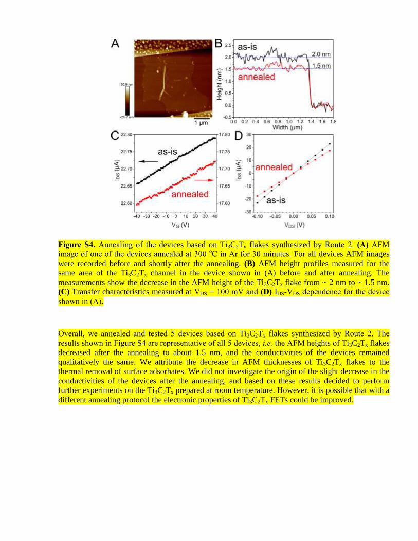
Figure S4. Annealing of the devices based on Ti3C2Tx flakes synthesized by Route 2. (A) AFM
image of one of the devices annealed at 300 oC in Ar for 30 minutes. For all devices AFM images
were recorded before and shortly after the annealing. (B) AFM height profiles measured for the
same area of the Ti3C2Tx channel in the device shown in (A) before and after annealing. The
measurements show the decrease in the AFM height of the Ti3C2Tx flake from ~ 2 nm to ~ 1.5 nm.
(C) Transfer characteristics measured at VDS = 100 mV and (D) IDS-VDS dependence for the device
shown in (A).
Overall, we annealed and tested 5 devices based on Ti3C2Tx flakes synthesized by Route 2. The
results shown in Figure S4 are representative of all 5 devices, i.e. the AFM heights of Ti3C2Tx flakes
decreased after the annealing to about 1.5 nm, and the conductivities of the devices remained
qualitatively the same. We attribute the decrease in AFM thicknesses of Ti3C2Tx flakes to the
thermal removal of surface adsorbates. We did not investigate the origin of the slight decrease in the
conductivities of the devices after the annealing, and based on these results decided to perform
further experiments on the Ti3C2Tx prepared at room temperature. However, it is possible that with a
different annealing protocol the electronic properties of Ti3C2Tx FETs could be improved.
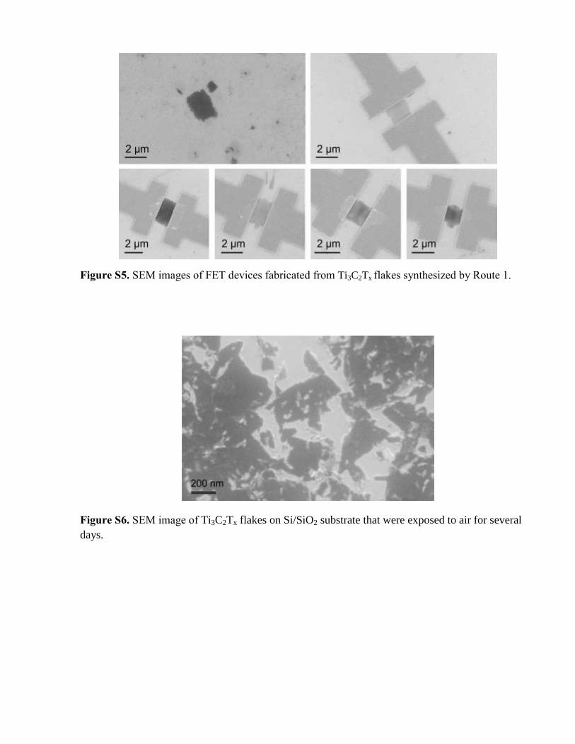
Figure S5. SEM images of FET devices fabricated from Ti3C2Tx flakes synthesized by Route 1.
Figure S6. SEM image of Ti3C2Tx flakes on Si/SiO2 substrate that were exposed to air for several
days.
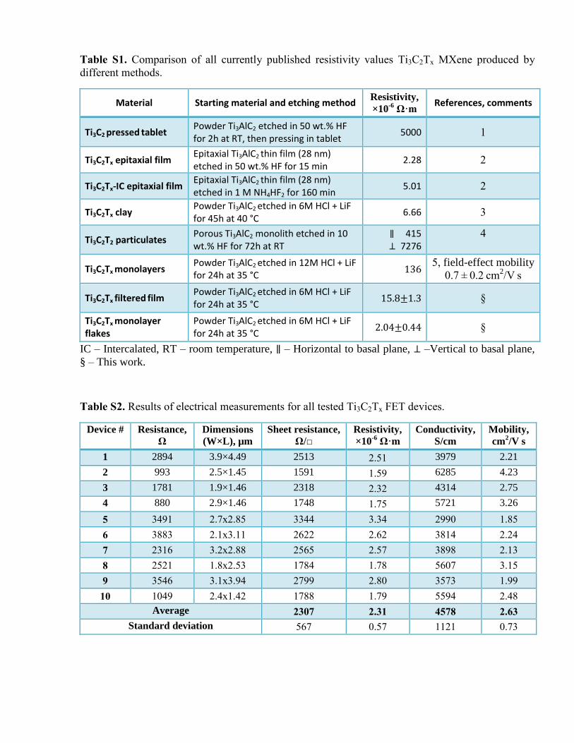
Table S1. Comparison of all currently published resistivity values Ti3C2Tx MXene produced by
different methods.
Material Starting material and etching method Resistivity,
×10-6
Ω·m References, comments
Ti3C2 pressed tablet Powder Ti3AlC2 etched in 50 wt.% HF for 2h at RT, then pressing in tablet
5000 1
Ti3C2Tx epitaxial film Epitaxial Ti3AlC2 thin film (28 nm) etched in 50 wt.% HF for 15 min
2.28 2
Ti3C2Tx-IC epitaxial film Epitaxial Ti3AlC2 thin film (28 nm) etched in 1 M NH4HF2 for 160 min
5.01 2
Ti3C2Tx clay Powder Ti3AlC2 etched in 6M HCl + LiF for 45h at 40 °C
6.66 3
Ti3C2T2 particulates Porous Ti3AlC2 monolith etched in 10 wt.% HF for 72h at RT
∥ 415 ⊥ 7276
4
Ti3C2Tx monolayers Powder Ti3AlC2 etched in 12M HCl + LiF for 24h at 35 °C
136 5, field-effect mobility
0.7 ± 0.2 cm2/V s
Ti3C2Tx filtered film Powder Ti3AlC2 etched in 6M HCl + LiF for 24h at 35 °C
15.8±1.3 §
Ti3C2Tx monolayer flakes
Powder Ti3AlC2 etched in 6M HCl + LiF for 24h at 35 °C
2.04±0.44 §
IC – Intercalated, RT – room temperature, ∥ – Horizontal to basal plane, ⊥ –Vertical to basal plane,
§ – This work.
Table S2. Results of electrical measurements for all tested Ti3C2Tx FET devices.
Device # Resistance,
Ω
Dimensions
(W×L), µm
Sheet resistance,
Ω/□
Resistivity,
×10-6
Ω·m
Conductivity,
S/cm
Mobility,
cm2/V s
1 2894 3.9×4.49 2513 2.51 3979 2.21
2 993 2.5×1.45 1591 1.59 6285 4.23
3 1781 1.9×1.46 2318 2.32 4314 2.75
4 880 2.9×1.46 1748 1.75 5721 3.26
5 3491 2.7x2.85 3344 3.34 2990 1.85
6 3883 2.1x3.11 2622 2.62 3814 2.24
7 2316 3.2x2.88 2565 2.57 3898 2.13
8 2521 1.8x2.53 1784 1.78 5607 3.15
9 3546 3.1x3.94 2799 2.80 3573 1.99
10 1049 2.4x1.42 1788 1.79 5594 2.48
Average 2307 2.31 4578 2.63
Standard deviation 567 0.57 1121 0.73
REFERENCES
1. Naguib, M.; Mashtalir, O.; Carle, J.; Presser, V.; Lu, J.; Hultman, L.; Gogotsi, Y.; Barsoum, M.
W. Two-Dimensional Transition Metal Carbides. ACS Nano 2012, 6, 1322-1331.
2. Halim, J.; Lukatskaya, M. R.; Cook, K. M.; Lu, J.; Smith, C. R.; Naslund, L. A.; May, S. J.;
Hultman, L.; Gogotsi, Y.; Eklund, P.; Barsoum, M. W. Transparent Conductive Two-
Dimensional Titanium Carbide Epitaxial Thin Films. Chem. Mater. 2014, 26, 2374-2381.
3. Ghidiu, M.; Lukatskaya, M. R.; Zhao, M. Q.; Gogotsi, Y.; Barsoum, M. W. Conductive two-
dimensional titanium carbide 'clay' with high volumetric capacitance. Nature 2014, 516, 78-81.
4. Hu, T.; Zhang, H.; Wang, J.; Li, Z.; Hu, M.; Tan, J.; Hou, P.; Li, F.; Wang, X. Anisotropic
electronic conduction in stacked two-dimensional titanium carbide. Scientific Reports 2015, 5,
16329.
5. Miranda, A.; Halim, J.; Barsoum, M. W.; Lorke, A. Electronic properties of freestanding
Ti3C2Tx MXene monolayers. Appl. Phys. Lett. 2016, 108, 033102.


![to Aza[5]helicene Viologen Acceptors Electronic Supplementary … · 2019. 6. 10. · Electronic Supplementary Information (ESI) for Synthesis, Structure and Photophysical Properties](https://img.pdfslide.us/doc/110x75/6021307fdedf18243b579090/to-aza5helicene-viologen-acceptors-electronic-supplementary-2019-6-10-electronic.jpg)