Embed Size (px)
Citation preview

ARTICLE IN PRESS
Nuclear Instruments and Methods in Physics Research A 610 (2009) 393–396
Contents lists available at ScienceDirect
Nuclear Instruments and Methods inPhysics Research A
0168-90
doi:10.1
� Corr
E-m
journal homepage: www.elsevier.com/locate/nima
Effect of SSPM surface coating on light collection efficiency and opticalcrosstalk for scintillation detection
Paul Barton a,�, Christopher Stapels b, Erik Johnson b, James Christian b, William W. Moses c,Martin Janecek c, David Wehe a
a University of Michigan, Ann Arbor, MI, USAb Radiation Monitoring Devices, Inc., Watertown, MAc Lawrence Berkeley National Laboratory, Berkeley, CA
a r t i c l e i n f o
Available online 6 June 2009
Keywords:
Silicon photomultipliers
Scintillation detectors
Optical system design
02/$ - see front matter & 2009 Elsevier B.V. A
016/j.nima.2009.05.187
esponding author. Tel.: +1734 615 5643; fax:
ail address: [email protected] (P. Barton).
a b s t r a c t
As part of a project to develop a complete stochastic model of the solid state photomultiplier (SSPM), we
simulated the effects of a reflective layer in the non-active region which reflects photons back into the
crystal for a second chance at detection. The scintillation photon collection efficiency of the proposed
device is greater than that predicted by the scintillation yield and the ratio of active area. The added
reflectivity also increases external optical crosstalk from hot carrier emissions and the collection
efficiency for these photons was simulated to be of the same order as the scintillation photon collection
efficiency. As a function of excess bias, the rate of hot carrier emissions will rise more rapidly than the
photon detection efficiency (PDE), setting a practical upper limit on the applied bias. Due to spectral
mismatch between detection and avalanche emission, a blue-sensitve SSPM will be largely transparent
to its own emissions. The spatial dependence of externally reflected hot carrier emissions was
determined to be approximately uniform.
& 2009 Elsevier B.V. All rights reserved.
1. Motivation
Our work seeks to develop a complete stochastic model of theSSPM. While the first-order statistics depend primarily on simpledevice parameters, the second-order statistics are composed ofseveral non-trivial noise mechanisms. This work is primarilyfocused on the use of SSPMs for the readout of scintillatingcrystals. A crystal in close contact with a photodetector representsa closed optical system in which the photodetector response maydepart from that of an open optical system (e.g. laser ranging).
The first difference we consider lies in the ability of the SSPMsurface to reflect incoming photons back into the crystal. Thealuminum readout lines necessary for inter-pixel connection maybe highly reflective and may also be made to fill the entire deadarea between active pixels. The addition of this aluminum-filllayer increases the photon detection efficiency (PDE) of the deviceby giving scintillation photons, which would have been lost in anopen optical system, a second chance at detection. The ability ofthe crystal to return these SSPM-reflected photons back onto theSSPM will depend on the optical properties of the entire system.
ll rights reserved.
+1734763 4540.
2. Surface reflectivity
In a commercial silicon foundry, the optical properties of thedeposited aluminum can vary significantly from process toprocess. Evaporated aluminum surfaces have been realized withreflectivities of 94% at a wavelength of 350 nm.
Radiation Monitoring Devices Inc. produced a die (modelAE215) containing four SSPMs with varying pixel width and pitch(cf. Table 1). An additional aluminum layer adds reflectivity overthe entire non-active area. This layer is not perfectly planar due tothe readout lines and silicon dioxide below.
The reflectivity of this SSPM was measured at LawrenceBerkeley National Laboratory using an apparatus recently de-signed to measure the reflectance of scintillation crystals andtheir reflectors [1]. A 440 nm laser was focused into a 0.7 mmdiameter spot on the surface of the SSPM and an arched bank ofphotodiodes recorded the reflected intensity over a solid angle of2p. After correcting the measurements for interference effects andthe non-planar geometry of the aluminum, the reflectance wasdetermined to be 80% at 440 nm.
3. Photon collection efficiency
To determine the degree of photon detection efficiencyimprovement from an additional aluminum layer, an optical
ARTICLE IN PRESS
Table 1Geometry of four quadrants in the RMD AE215 SSPM.
Pixel width
(mm)
Inter-pixel
(mm)
Pixels
across
Fill factor
(%)
Al fill
(%)
Q1 30 14 31 49 51
Q2 50 14 21 61 39
Q3 50 26 18 43 57
Q4 30 26 24 29 71
1
0.8
0.6
0.4
0.2
00 0.2 0.4 0.6 0.8 1
Fill Factor
Col
lect
ion
Effi
cien
cy
80% Al Refl.Si Absorb.
Fig. 1. The simulated photon collection efficiency as a function of SSPM fill factor
for a Teflon-wrapped cubic crystal on an absorptive (dashed line) or semi-reflective
(solid line) detection surface. The results include losses due to surface absorption
in the Teflon.
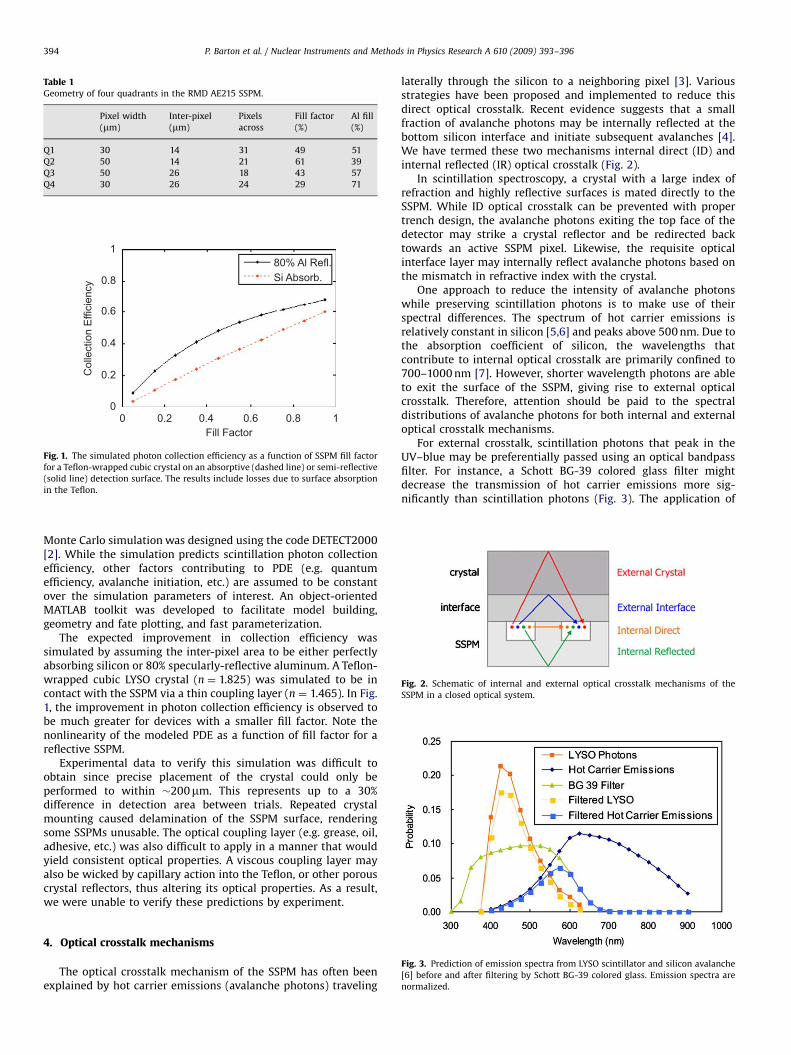
Fig. 2. Schematic of internal and external optical crosstalk mechanisms of the
SSPM in a closed optical system.
P. Barton et al. / Nuclear Instruments and Methods in Physics Research A 610 (2009) 393–396394
Monte Carlo simulation was designed using the code DETECT2000[2]. While the simulation predicts scintillation photon collectionefficiency, other factors contributing to PDE (e.g. quantumefficiency, avalanche initiation, etc.) are assumed to be constantover the simulation parameters of interest. An object-orientedMATLAB toolkit was developed to facilitate model building,geometry and fate plotting, and fast parameterization.
The expected improvement in collection efficiency wassimulated by assuming the inter-pixel area to be either perfectlyabsorbing silicon or 80% specularly-reflective aluminum. A Teflon-wrapped cubic LYSO crystal (n ¼ 1.825) was simulated to be incontact with the SSPM via a thin coupling layer (n ¼ 1.465). In Fig.1, the improvement in photon collection efficiency is observed tobe much greater for devices with a smaller fill factor. Note thenonlinearity of the modeled PDE as a function of fill factor for areflective SSPM.
Experimental data to verify this simulation was difficult toobtain since precise placement of the crystal could only beperformed to within �200mm. This represents up to a 30%difference in detection area between trials. Repeated crystalmounting caused delamination of the SSPM surface, renderingsome SSPMs unusable. The optical coupling layer (e.g. grease, oil,adhesive, etc.) was also difficult to apply in a manner that wouldyield consistent optical properties. A viscous coupling layer mayalso be wicked by capillary action into the Teflon, or other porouscrystal reflectors, thus altering its optical properties. As a result,we were unable to verify these predictions by experiment.
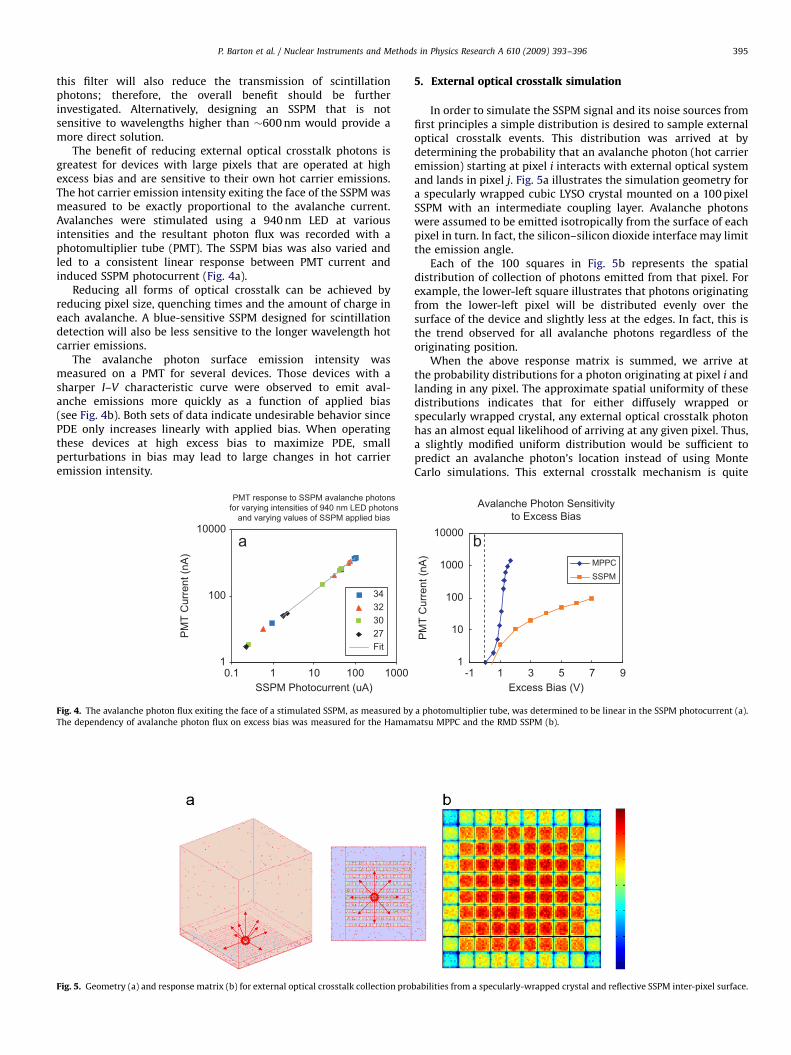
Fig. 3. Prediction of emission spectra from LYSO scintillator and silicon avalanche
[6] before and after filtering by Schott BG-39 colored glass. Emission spectra are
normalized.
4. Optical crosstalk mechanisms
The optical crosstalk mechanism of the SSPM has often beenexplained by hot carrier emissions (avalanche photons) traveling
laterally through the silicon to a neighboring pixel [3]. Variousstrategies have been proposed and implemented to reduce thisdirect optical crosstalk. Recent evidence suggests that a smallfraction of avalanche photons may be internally reflected at thebottom silicon interface and initiate subsequent avalanches [4].We have termed these two mechanisms internal direct (ID) andinternal reflected (IR) optical crosstalk (Fig. 2).
In scintillation spectroscopy, a crystal with a large index ofrefraction and highly reflective surfaces is mated directly to theSSPM. While ID optical crosstalk can be prevented with propertrench design, the avalanche photons exiting the top face of thedetector may strike a crystal reflector and be redirected backtowards an active SSPM pixel. Likewise, the requisite opticalinterface layer may internally reflect avalanche photons based onthe mismatch in refractive index with the crystal.
One approach to reduce the intensity of avalanche photonswhile preserving scintillation photons is to make use of theirspectral differences. The spectrum of hot carrier emissions isrelatively constant in silicon [5,6] and peaks above 500 nm. Due tothe absorption coefficient of silicon, the wavelengths thatcontribute to internal optical crosstalk are primarily confined to700–1000 nm [7]. However, shorter wavelength photons are ableto exit the surface of the SSPM, giving rise to external opticalcrosstalk. Therefore, attention should be paid to the spectraldistributions of avalanche photons for both internal and externaloptical crosstalk mechanisms.
For external crosstalk, scintillation photons that peak in theUV–blue may be preferentially passed using an optical bandpassfilter. For instance, a Schott BG-39 colored glass filter mightdecrease the transmission of hot carrier emissions more sig-nificantly than scintillation photons (Fig. 3). The application of
ARTICLE IN PRESS
P. Barton et al. / Nuclear Instruments and Methods in Physics Research A 610 (2009) 393–396 395
this filter will also reduce the transmission of scintillationphotons; therefore, the overall benefit should be furtherinvestigated. Alternatively, designing an SSPM that is notsensitive to wavelengths higher than �600 nm would provide amore direct solution.
The benefit of reducing external optical crosstalk photons isgreatest for devices with large pixels that are operated at highexcess bias and are sensitive to their own hot carrier emissions.The hot carrier emission intensity exiting the face of the SSPM wasmeasured to be exactly proportional to the avalanche current.Avalanches were stimulated using a 940 nm LED at variousintensities and the resultant photon flux was recorded with aphotomultiplier tube (PMT). The SSPM bias was also varied andled to a consistent linear response between PMT current andinduced SSPM photocurrent (Fig. 4a).
Reducing all forms of optical crosstalk can be achieved byreducing pixel size, quenching times and the amount of charge ineach avalanche. A blue-sensitive SSPM designed for scintillationdetection will also be less sensitive to the longer wavelength hotcarrier emissions.
The avalanche photon surface emission intensity wasmeasured on a PMT for several devices. Those devices with asharper I–V characteristic curve were observed to emit aval-anche emissions more quickly as a function of applied bias(see Fig. 4b). Both sets of data indicate undesirable behavior sincePDE only increases linearly with applied bias. When operatingthese devices at high excess bias to maximize PDE, smallperturbations in bias may lead to large changes in hot carrieremission intensity.
PMT response to SSPM avalanche photonsfor varying intensities of 940 nm LED photons
and varying values of SSPM applied bias
1
100
10000
SSPM Photocurrent (uA)
PM
T C
urre
nt (n
A)
34323027Fit
0.1 1 10 100 1000
Fig. 4. The avalanche photon flux exiting the face of a stimulated SSPM, as measured by
The dependency of avalanche photon flux on excess bias was measured for the Hamam
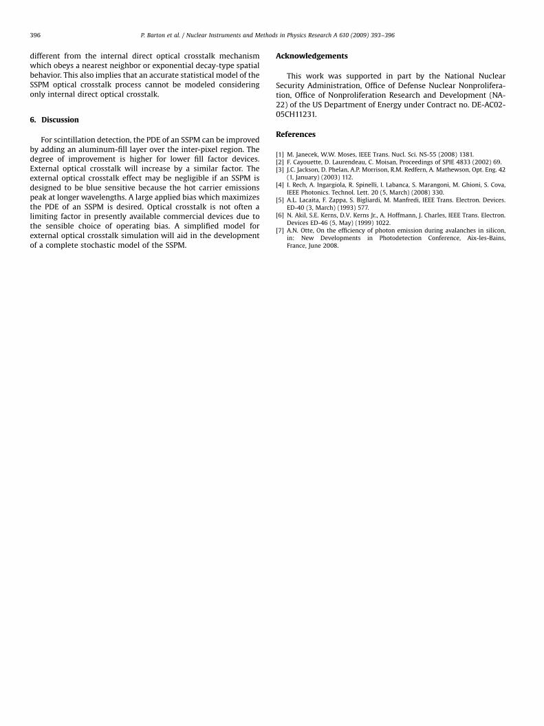
Fig. 5. Geometry (a) and response matrix (b) for external optical crosstalk collection pro
5. External optical crosstalk simulation
In order to simulate the SSPM signal and its noise sources fromfirst principles a simple distribution is desired to sample externaloptical crosstalk events. This distribution was arrived at bydetermining the probability that an avalanche photon (hot carrieremission) starting at pixel i interacts with external optical systemand lands in pixel j. Fig. 5a illustrates the simulation geometry fora specularly wrapped cubic LYSO crystal mounted on a 100 pixelSSPM with an intermediate coupling layer. Avalanche photonswere assumed to be emitted isotropically from the surface of eachpixel in turn. In fact, the silicon–silicon dioxide interface may limitthe emission angle.
Each of the 100 squares in Fig. 5b represents the spatialdistribution of collection of photons emitted from that pixel. Forexample, the lower-left square illustrates that photons originatingfrom the lower-left pixel will be distributed evenly over thesurface of the device and slightly less at the edges. In fact, this isthe trend observed for all avalanche photons regardless of theoriginating position.
When the above response matrix is summed, we arrive atthe probability distributions for a photon originating at pixel i andlanding in any pixel. The approximate spatial uniformity of thesedistributions indicates that for either diffusely wrapped orspecularly wrapped crystal, any external optical crosstalk photonhas an almost equal likelihood of arriving at any given pixel. Thus,a slightly modified uniform distribution would be sufficient topredict an avalanche photon’s location instead of using MonteCarlo simulations. This external crosstalk mechanism is quite
Avalanche Photon Sensitivityto Excess Bias
1
10
100
1000
10000
-1 1 3 5 7 9Excess Bias (V)
PM
T C
urre
nt (n
A)
MPPCSSPM
a photomultiplier tube, was determined to be linear in the SSPM photocurrent (a).
atsu MPPC and the RMD SSPM (b).
babilities from a specularly-wrapped crystal and reflective SSPM inter-pixel surface.
ARTICLE IN PRESS
P. Barton et al. / Nuclear Instruments and Methods in Physics Research A 610 (2009) 393–396396
different from the internal direct optical crosstalk mechanismwhich obeys a nearest neighbor or exponential decay-type spatialbehavior. This also implies that an accurate statistical model of theSSPM optical crosstalk process cannot be modeled consideringonly internal direct optical crosstalk.
6. Discussion
For scintillation detection, the PDE of an SSPM can be improvedby adding an aluminum-fill layer over the inter-pixel region. Thedegree of improvement is higher for lower fill factor devices.External optical crosstalk will increase by a similar factor. Theexternal optical crosstalk effect may be negligible if an SSPM isdesigned to be blue sensitive because the hot carrier emissionspeak at longer wavelengths. A large applied bias which maximizesthe PDE of an SSPM is desired. Optical crosstalk is not often alimiting factor in presently available commercial devices due tothe sensible choice of operating bias. A simplified model forexternal optical crosstalk simulation will aid in the developmentof a complete stochastic model of the SSPM.
Acknowledgements
This work was supported in part by the National NuclearSecurity Administration, Office of Defense Nuclear Nonprolifera-tion, Office of Nonproliferation Research and Development (NA-22) of the US Department of Energy under Contract no. DE-AC02-05CH11231.
References
[1] M. Janecek, W.W. Moses, IEEE Trans. Nucl. Sci. NS-55 (2008) 1381.[2] F. Cayouette, D. Laurendeau, C. Moisan, Proceedings of SPIE 4833 (2002) 69.[3] J.C. Jackson, D. Phelan, A.P. Morrison, R.M. Redfern, A. Mathewson, Opt. Eng. 42
(1, January) (2003) 112.[4] I. Rech, A. Ingargiola, R. Spinelli, I. Labanca, S. Marangoni, M. Ghioni, S. Cova,
IEEE Photonics. Technol. Lett. 20 (5, March) (2008) 330.[5] A.L. Lacaita, F. Zappa, S. Bigliardi, M. Manfredi, IEEE Trans. Electron. Devices.
ED-40 (3, March) (1993) 577.[6] N. Akil, S.E. Kerns, D.V. Kerns Jr., A. Hoffmann, J. Charles, IEEE Trans. Electron.
Devices ED-46 (5, May) (1999) 1022.[7] A.N. Otte, On the efficiency of photon emission during avalanches in silicon,
in: New Developments in Photodetection Conference, Aix-les-Bains,France, June 2008.