Embed Size (px)
Citation preview

EFFECT OF BIAS VOLTAGE WAVEFORMS ON ION ENERGY DISTRIBUTIONS
AND FLUOROCARBON PLASMA ETCH SELECTIVITY*
Ankur Agarwala) and Mark J. Kushnerb)
a)Department of Chemical and Biomolecular Engineering
Email: [email protected]
b)Department of Electrical and Computer Engineering Email: [email protected]
University of IllinoisUrbana, IL 61801, USA
http://uigelz.ece.uiuc.edu
51st AVS Symposium, November 2004
* Work supported by the NSF, SRC and VSEA

University of Illinois
Optical and Discharge Physics
AGENDA
Introduction
Bias Voltage Waveforms
Approach and Methodology
Ion Energy Distribution Functions
Fluorocarbon Etch Selectivity
Etching Recipes
Summary
ANKUR_AVS04_Agenda

University of Illinois
Optical and Discharge Physics
HIGH ETCH SELECTIVITY
High etch selectivity is a necessary characteristic for semiconductor manufacturing.
Prevents erosion of photoresist and/or underlying films. Permits over-etching to compensate for process nonuniformities.
ANKUR_AVS_01
Low Etch Selectivity Substrate damage Improper etch stop layer
High Etch Selectivity Little Substrate damage Proper etch stop layer

University of Illinois
Optical and Discharge Physics
ETCH MECHANISM
CFx and CxFy form a polymeric passivation layer which regulates delivery of etch precursors and activation energy.
Chemisorption of CFx produces a complex at the oxide-polymer interface.
ANKUR_AVS_02
CFx Ion+
I*, CF2
SiO2CxFy SiOCFy
CxFy
Ion+
CO2Ion+
CO2
Polymer
SiF3
Ion+,FSiF3
CFx
Polymer
F
SiF SiF2 SiF3
Ion+,F
SiF3
SiO2
Plasma
Si
CxFy
Plasma
PassivationLayer
CxFyPassivation
Layer
Low energy ion activation of the complex produces polymer.
The polymer layer is sputtered by energetic ions
The complex formed at the oxide-polymer interface undergoes ion activated dissociation to form volatile etch products (SiF3, CO2).

University of Illinois
Optical and Discharge Physics
ACHIEVING HIGH SELECTIVITY
ANKUR_AVS_03
Ref: S.-B. Wang and A.E. Wendt, J. Vac. Sci. Technol. A, 19, 2425 (2001)
High etch selectivity is achieved by controlling the ion energy distribution at the substrate.
Sinusoidal bias: Broad ion energy distribution does not discriminate thresholds (narrow process window).
Tailored bias: Produce a narrow ion energy distribution which discriminates between threshold energies (broad process window).
Ion activation scales inversely with polymer thickness, while polymer thickness scales inversely with bias.
Sinusoidal Bias
University of Illinois
Optical and Discharge Physics
VALIDATION OF REACTION MECHANISM
ANKUR_AVS_04
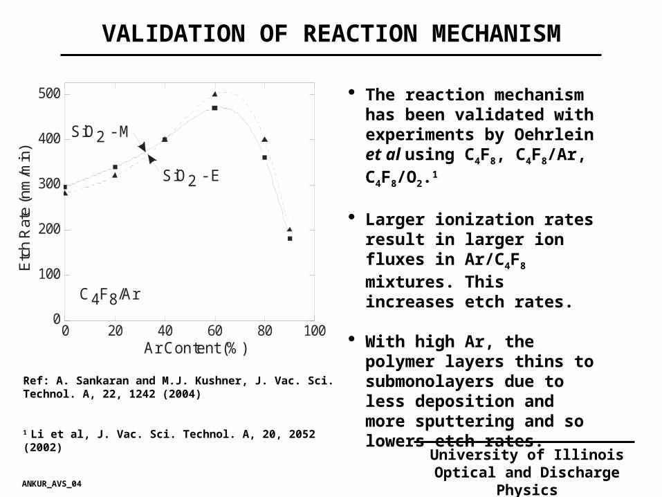
The reaction mechanism has been validated with experiments by Oehrlein et al using C4F8, C4F8/Ar, C4F8/O2.1
Larger ionization rates result in larger ion fluxes in Ar/C4F8 mixtures. This increases etch rates.
With high Ar, the polymer layers thins to submonolayers due to less deposition and more sputtering and so lowers etch rates.
0 20 40 60 80 1000
100
200
300
C4F8/O2
SiO2 - E
SiO2 - M
Etc
h R
ate
(nm
/min
)
O Content (%)2
0 20 40 60 80 1000
100
200
300
400
500
C4F8/Ar
SiO2 - E
SiO2 - M
Etc
h R
ate
(nm
/min
)
Ar Content (%)
Ref: A. Sankaran and M.J. Kushner, J. Vac. Sci. Technol. A, 22, 1242 (2004)
1 Li et al, J. Vac. Sci. Technol. A, 20, 2052 (2002)

University of Illinois
Optical and Discharge Physics
CUSTOM BIAS VOLTAGE WAVEFORMS
Ion Energy Distribution (IED) traditionally controlled by varying the amplitude of a sinusoidal voltage waveform.
Resultant IED – broad; both high and low energy ions
Specially tailored non-sinusoidal bias voltage waveform
Narrow IED at the substrate Peak of IED can be positioned to achieve desired selectivity
ANKUR_AVS_05
Synthesized voltage Waveform: Periodic Short voltage spike Ramp down
Ref: S.-B. Wang and A.E. Wendt, J. Vac. Sci. Technol. A, 19, 2425 (2001)
The “10% Waveform

University of Illinois
Optical and Discharge Physics
INTEGRATED MODELING
HPEM (Hybrid Plasma Equipment Model) is the reactor scale model platform.
Low pressure (<10’s Torr) 2-d and 3-d versions Address ICP, CCP, RIE
HPEM is linked to profile simulators – MCFPM (Monte Carlo Feature Profile Model) to predict the evolution of submicron features.
2-d and 3-d Fluxes from HPEM
ANKUR_AVS_06
An integrated reactor and feature scale modeling hierarchy was developed to model plasma processing systems.

University of Illinois
Optical and Discharge Physics
HYBRID PLASMA EQUIPMENT MODEL
ANKUR_AVS_07
A modular simulator addressing low temperature, low pressure plasmas.
Electro-magnetic Module: Electromagnetic Fields Magneto-static Fields
Electron Energy Transport Module: Electron Temperature Electron Impact Sources Transport Coefficients
Fluid Kinetics Module: Densities Momenta Temperature of species Electrostatic Potentials

University of Illinois
Optical and Discharge Physics
MONTE CARLO FEATURE PROFILE MODEL
ANKUR_AVS_08
Monte Carlo based model to address plasma surface interactions and evolution of surface morphology and profiles.
Inputs:
Initial material mesh Etch mechanisms (chemical rxn. format) Energy and Angular dependence Gas species flux distribution used to
determine the launching and direction of incoming particles.
Flux distributions from equipment scale model (HPEM)

University of Illinois
Optical and Discharge Physics
DYNAMIC SIMULATION – REACTOR SCALE
Transformer-coupled plasma (TCP) reactor geometry
To accelerate ions to the wafer, a rf bias voltage is applied.
Base case conditions: Ar/C4F8 = 75/25, 100 sccm 15 mTorr, 500 W 200 Vp-p, 5 MHz “10%” Voltage Waveform
ANKUR_AVS_09

University of Illinois
Optical and Discharge Physics
REACTANT FLUXES
ANKUR_AVS_10
Polymer formation – Low energy process
Polymer sputtering and etch activation – High energy
15 mTorr, 500 W, 200 Vp-p,Ar/C4F8 = 75/25, 100 sccm
Dominant Ions: Ar+, CF3+, CF+
Dominant Neutrals: CF, C2F3, F
University of Illinois
Optical and Discharge Physics
ION ENERGY DISTRIBUTION FUNCTIONS
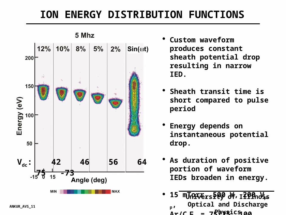
Custom waveform produces constant sheath potential drop resulting in narrow IED.
Sheath transit time is short compared to pulse period
Energy depends on instantaneous potential drop.
As duration of positive portion of waveform IEDs broaden in energy.
15 mTorr, 500 W, 200 Vp-p,Ar/C4F8 = 75/25, 100 sccm
ANKUR_AVS_11
Vdc: 42 46 56 64 75 -73
University of Illinois
Optical and Discharge Physics
IEAD vs CUSTOM BIAS WAVEFORMS
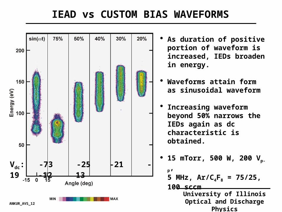
As duration of positive portion of waveform is increased, IEDs broaden in energy.
Waveforms attain form as sinusoidal waveform
Increasing waveform beyond 50% narrows the IEDs again as dc characteristic is obtained.
15 mTorr, 500 W, 200 Vp-p,5 MHz, Ar/C4F8 = 75/25, 100 sccm
ANKUR_AVS_12
Vdc: -73 -25 -21 -19 -12 13

University of Illinois
Optical and Discharge Physics
IEAD vs CUSTOM BIAS VOLTAGE
The peak energy of the IEAD is controlled by amplitude and frequency.
IED broadens at higher biases due to thickening of sheath and longer transit times.
IED still narrower compared to sinusoidal voltage waveform.
15 mTorr, 500 W,Ar/C4F8 = 75/25, 100 sccm
ANKUR_AVS_13
University of Illinois
Optical and Discharge Physics
ETCH PROFILES – CUSTOM VOLTAGE WAVEFORM
ANKUR_AVS_14
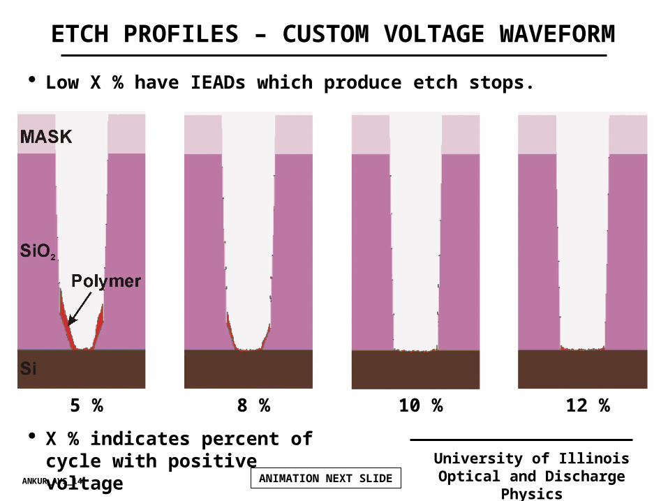
5 % 8 % 10 % 12 %
ANIMATION NEXT SLIDE
X % indicates percent of cycle with positive voltage
Low X % have IEADs which produce etch stops.
University of Illinois
Optical and Discharge Physics
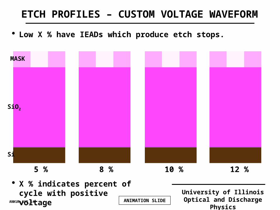
ETCH PROFILES – CUSTOM VOLTAGE WAVEFORM
ANKUR_AVS_14
5 % 8 % 10 % 12 %
ANIMATION SLIDE
MASK
SiO2
Si
X % indicates percent of cycle with positive voltage
Low X % have IEADs which produce etch stops.
University of Illinois
Optical and Discharge Physics
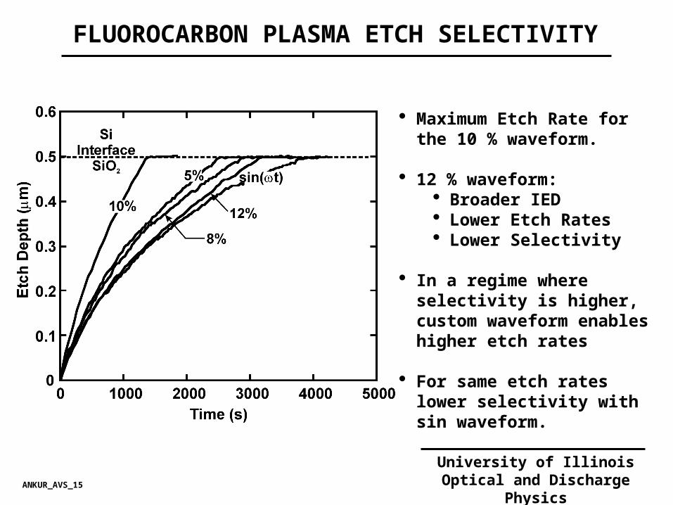
FLUOROCARBON PLASMA ETCH SELECTIVITY
Maximum Etch Rate for the 10 % waveform.
12 % waveform: Broader IED Lower Etch Rates Lower Selectivity
In a regime where selectivity is higher, custom waveform enables higher etch rates
For same etch rates lower selectivity with sin waveform.
ANKUR_AVS_15
University of Illinois
Optical and Discharge Physics
ETCH PROFILES – CUSTOM VOLTAGE PEAK-TO-PEAK
ANKUR_AVS_16
400 V 500 V 1000 V 1500 V
XXX V indicates amplitude of bias
Increasing bias increases etch rate and reduces selectivity.
ANIMATION NEXT SLIDE

University of Illinois
Optical and Discharge Physics
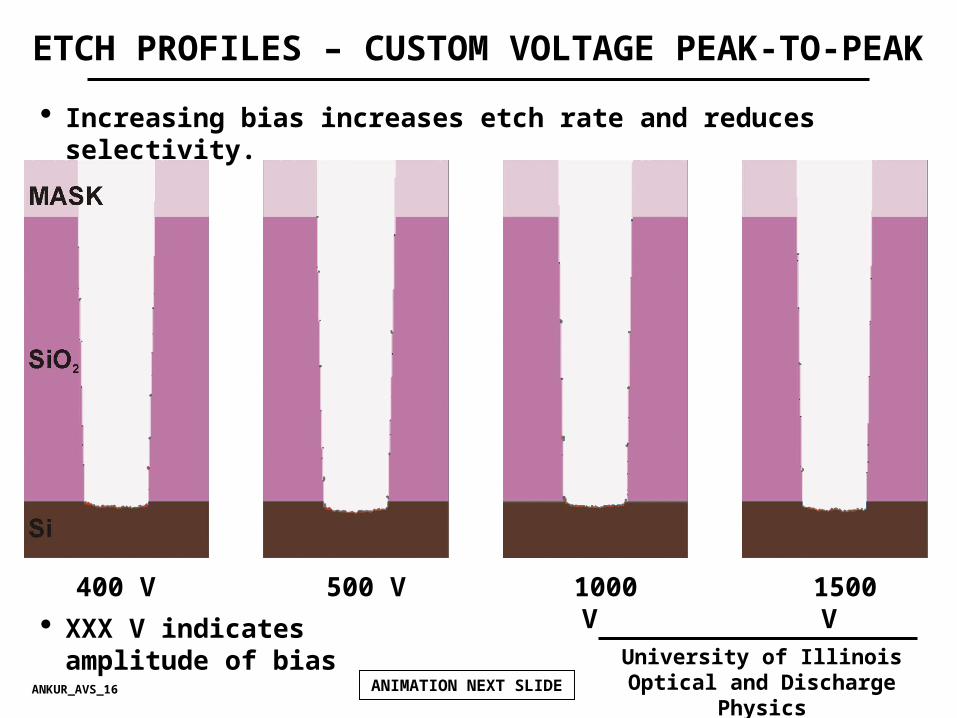
ETCH PROFILES – CUSTOM VOLTAGE PEAK-TO-PEAK
ANKUR_AVS_16ANIMATION SLIDE
400 V 500 V 1000 V 1500 V
XXX V indicates amplitude of bias
Increasing bias increases etch rate and reduces selectivity.
MASK
SiO2
Si
University of Illinois
Optical and Discharge Physics
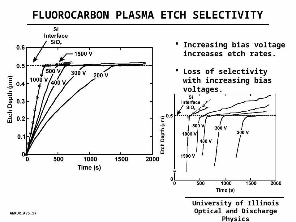
FLUOROCARBON PLASMA ETCH SELECTIVITY
Increasing bias voltage increases etch rates.
Loss of selectivity with increasing bias voltages.
ANKUR_AVS_17

University of Illinois
Optical and Discharge Physics
ETCHING RECIPES
Multi-component recipes:
Main-etch: Non selective; High bias Over-etch: Selective; Low bias
Traditionally, gas mixture is changed to obtain a selective etch.
Controlling chemical component Clearing of gases is determined by
residence time Finite selectivity
Custom tailored voltage waveform
Controlling physical component Change amplitude – immediate
control “Infinite” selectivity
ANKUR_AVS_18

University of Illinois
Optical and Discharge Physics
ETCHING PROFILES – RECIPE
ANKUR_AVS_19 ANIMATION NEXT SLIDE
200 V(Slow, selective)
1500 V(Fast, non-selective)
1500/200 V(Fast, selective)
1500/1000/100/200 V(Fast, selective)

University of Illinois
Optical and Discharge Physics
ETCHING PROFILES – RECIPE
ANKUR_AVS_19 ANIMATION SLIDE
200 V(Slow, selective)
1500 V(Fast, non-selective)
1500/200 V(Fast, selective)
MASK
SiO2
Si
1500/1000/100/200 V(Fast, selective)
1847 s 713 s 1377 s 1356 s

University of Illinois
Optical and Discharge Physics
SUMMARY
Higher etch selectivity was obtained by controlling ion energy distribution.
Flux, Energy and Angular distribution optimized to attain high etch selectivity
Special tailored voltage waveform was synthesized.
Short voltage spike followed by ramp down Results in a narrow IED over wide range of voltages and
frequency.
New etching recipe
Based only on bias voltage amplitude without changing gas chemistry.
Excellent control over selectivity demonstrated.
ANKUR_AVS_20