Embed Size (px)
Citation preview

EEM 486: Computer Architecture
Lecture 3
Designing a Single Cycle Datapath

Lec 3.2
The Big Picture: Where are We Now?
The Five Classic Components of a Computer
Today’s Topic: Design a Single Cycle Processor
Control
Datapath
Memory
ProcessorInput
Output

Lec 3.3
The Big Picture: The Performance Perspective
Performance of a machine is determined by:
• Instruction count
• Clock cycle time
• Clock cycles per instruction
Processor design (datapath and control) will determine:
• Clock cycle time
• Clock cycles per instruction
CPI
Inst. Count Cycle Time

Lec 3.4
Single-cycle datapath
All instructions execute in a single cycle of the clock (positive edge to positive edge)
Advantage: a great way to learn CPU
Unrealistic hardware assumptions, slow clock period

Lec 3.5
Single cycle data paths: Assumptions
Processor uses synchronous logicdesign (a “clock”)
f T
1 MHz 1 μs
10 MHz 100 ns
100 MHz 10 ns
1 GHz 1 ns
• All state elements act like positive edge-triggered flip flops
• Clocks arrive at all flip flops simultaneously.
D Q
clk

Lec 3.6
Review: Edge-Triggered D Flip Flops
D Q Value of D is sampled on positive clock edge
Q outputs sampled value for rest of cycle.
CLK
D
Q

Lec 3.7
How to Design a Processor: Step-by-Step
1. Analyze instruction set => datapath requirements• Meaning of each instruction is given by the register transfers
• Datapath must include storage element for ISA registers
- possibly more
• Datapath must support each register transfer
2. Select set of datapath components and establish clocking methodology
3. Assemble datapath meeting the requirements
4. Analyze implementation of each instruction to determine setting of control points that effects the register transfer
5. Assemble the control logic

Lec 3.8
The MIPS Instruction Formats
The three instruction formats:
• R-type
• I-type
• J-type
The different fields are:• op: operation of the instruction• rs, rt, rd: the source and destination register specifiers• shamt: shift amount• funct: selects the variant of the operation in the “op” field• address / immediate: address offset or immediate value• target address: target address of the jump instruction
op target address
02631
6 bits 26 bits
op rs rt rd shamt funct
061116212631
6 bits 6 bits5 bits5 bits5 bits5 bits
op rs rt immediate016212631
6 bits 16 bits5 bits5 bits

Lec 3.9
Step 1a: The MIPS-lite Subset for Today
ADD/SUB
• addU rd, rs, rt
• subU rd, rs, rt
OR Immediate:
• ori rt, rs, imm16
LOAD/STORE Word
• lw rt, rs, imm16
• sw rt, rs, imm16
BRANCH
• beq rs, rt, imm16
op rs rt rd shamt funct
061116212631
6 bits 6 bits5 bits5 bits5 bits5 bits
op rs rt immediate
016212631
6 bits 16 bits5 bits5 bits
op rs rt immediate
016212631
6 bits 16 bits5 bits5 bits
op rs rt immediate
016212631
6 bits 16 bits5 bits5 bits

Lec 3.10
Step 1a: Executing MIPS Instructions
- Fetch next inst from memory - Get ready for the next instruction
opcode rs rt rd functshamt
- Decode fields to get a particular instruction
- Retrieve register values (rs, rt)
- Perform the operation (add, sub, or, lw, sw, beq)
- Place the result in a register (rt/rd) / memory, ormodify PC
InstructionFetch
InstructionDecode
OperandFetch
Execute
ResultStore

Lec 3.11
Step 1a: Logical Register Transfers RTL gives the meaning of the instructions
All start by fetching the instruction
op | rs | rt | rd | shamt | funct = MEM[ PC ]
op | rs | rt | Imm16 = MEM[ PC ]
inst Register Transfers
ADDU R[rd] <– R[rs] + R[rt]; PC <– PC + 4
SUBU R[rd] <– R[rs] – R[rt]; PC <– PC + 4
ORi R[rt] <– R[rs] | zero_ext(Imm16); PC <– PC + 4
LOAD R[rt] <– MEM[ R[rs] + sign_ext(Imm16)]; PC <– PC + 4
STORE MEM[ R[rs] + sign_ext(Imm16) ] <– R[rt]; PC <– PC + 4
BEQ if ( R[rs] == R[rt] ) then PC <– PC + 4 + [sign_ext(Imm16) || 00] else PC <– PC + 4

Lec 3.12
Step 1: Requirements of the Instruction Set Memory
• instruction & data
Registers (32 x 32)
• read RS
• read RT
• Write RT or RD
PC
Extender
Add and Sub registers or register and extended immediate
Logical Or of a register and extended immediate
Add 4 or extended immediate to PC

Lec 3.13
Step 2: Components of the Datapath
Combinational Elements
Storage Elements
• Clocking methodology

Lec 3.14
Combinational Logic Elements (Basic Building Blocks)
Adder
MUX
ALU
32
32
A
B
32Sum
Carry
32
32
A
B
32Result
OP
32A
B32
Y32
Select
Adder
MU
XA
LU
CarryIn

Lec 3.15
Storage Element: Register (Basic Building Block)
Register• Similar to the D Flip Flop except
- N-bit input and output
- Write Enable input
• Write Enable:
- Negated (0): Data Out will not change
- Asserted (1): Data Out becomes Data InClk
Data In
Write Enable
N N
Data Out

Lec 3.16
Storage Element: Register File Register File consists of 32 registers:
• Two 32-bit output busses:
busA and busB
• One 32-bit input bus: busW
Register is selected by:• RA (number) selects the register to put on busA (data)
• RB (number) selects the register to put on busB (data)
• RW (number) selects the register to be writtenvia busW (data) when Write Enable is 1
Clock input (CLK) • The CLK input is a factor ONLY during write operation
• During read operation, behaves as a combinational logic block:
- RA or RB valid => busA or busB valid after “access time.”
Clk
busW
Write Enable
3232
busA
32busB
5 5 5RW RA RB
32 32-bitRegisters

Lec 3.17
Storage Element: Idealized Memory
Memory (idealized)• One input bus: Data In
• One output bus: Data Out
Memory word is selected by:• Address selects the word to put on Data Out
• Write Enable = 1: address selects the memoryword to be written via the Data In bus
Clock input (CLK) • The CLK input is a factor ONLY during write operation
• During read operation, behaves as a combinational logic block:
- Address valid => Data Out valid after “access time.”
Clk
Data In
Write Enable
32 32DataOut
Address

Lec 3.18
Clocking Methodology
All storage elements are clocked by the same clock edge Being physical devices, flip-flops (FF) and combinational logic
have some delays • Gates: delay from input change to output change • Signals at FF D input must be stable before active clock edge to
allow signal to travel within the FF, and we have the usual clock-to-Q delay
“Critical path” (longest path through logic) determines length of clock period
.
.
.
.
.
.
.
.
.
.
.
.
Clk
Don’t Care
Setup HoldSetup Hold

Lec 3.19
Step 3: Assemble Datapath Meeting Requirements
Register Transfer Requirements Datapath Assembly
Instruction Fetch
Read Operands and Execute Operation

Lec 3.20
3a: Overview of the Instruction Fetch Unit The common RTL operations
• Fetch the Instruction: mem[PC]
- PC == Program Counter, points to next instruction• Update the program counter:
- Sequential Code: PC <- PC + 4
- Branch and Jump: PC <- “something else”
32
Instruction WordAddress
InstructionMemory
PCClk
Next AddressLogic

Lec 3.21
Straight-line Instruction Fetch
32
Addr
Data
32
InstrMem
Why +4 and not +1?
CLK
Address
Data IMem[PC + 8]
IMem[PC + 4]IMem[PC]
PC + 8PC + 4PC
op target address02631
6 bits 26 bits
op rs rt rd shamt funct061116212631
6 bits 6 bits5 bits5 bits5 bits5 bits
op rs rt immediate016212631
6 bits 16 bits5 bits5 bits

Lec 3.22
3b: Add & Subtract R[rd] <- R[rs] op R[rt] Example: addU rd, rs, rt
• Ra, Rb, and Rw come from instruction’s rs, rt, and rd fields
• ALUctr and RegWr: control logic produces after decoding the instruction
32
Result
ALUctr
Clk
busW
RegWr
32
32
busA
32
busB
5 5 5
Rw Ra Rb
32 32-bitRegisters
Rs RtRd
ALU
op rs rt rd shamt funct
061116212631
6 bits 6 bits5 bits5 bits5 bits5 bits
Lec 3.23
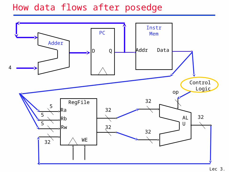
How data flows after posedge
32
RegFile
32
WE32
5Ra
5Rb
5Rw
32ALU
32
32
op
Control Logic
Addr Data
InstrMem
D
PC
Q
Adder
4

Lec 3.24
Register-Register Timing: One complete cycle
32
Result
ALUctr
Clk
busW
RegWr
3232
busA
32busB
5 5 5
Rw Ra Rb
32 32-bitRegisters
Rs RtRd
ALU
Clk
PC
Rs, Rt, Rd,Op, Func
Clk-to-Q
ALUctr
Instruction Memory Access Time
Old Value New Value
RegWr Old Value New Value
Delay through Control Logic
busA, B
Register File Access Time
Old Value New Value
busW
ALU Delay
Old Value New Value
Old Value New Value
New ValueOld Value
Register WriteOccurs Here

Lec 3.25
3c: Logical Operations with Immediate R[rt] <- R[rs] op ZeroExt[imm16]
op rs rt immediate
016212631
6 bits 16 bits5 bits5 bits
32
Result
ALUctr
Clk
busW
RegWr
32
32
busA
32
busB
5 5 5
Rw Ra Rb
32 32-bitRegisters
Rs
Zero
Ext
Mu
x
RtRdRegDst
Mux
3216imm16
ALUSrc
ALU
Rt?

Lec 3.26
3d: Load Operations R[rt] <- Mem[R[rs] + SignExt[imm16]] E.g.: lw rt, rs,
imm16
op rs rt immediate
016212631
6 bits 16 bits5 bits5 bits
32
ALUctr
Clk
busW
RegWr
3232
busA
32busB
5 5 5
Rw Ra Rb32 32-bitRegisters
Rs
RtRdRegDst
Exte
nd
er
Mu
x
Mux
3216
imm16
ALUSrc
ExtOp
Clk
Data InWrEn
32
Adr
DataMemory
32
ALU
MemWr Mu
x
W_Src
??
Rt?

Lec 3.27
3e: Store Operations
Mem[ R[rs] + SignExt[imm16] ] <- R[rt] E.g.: sw rt, rs, imm16
op rs rt immediate
016212631
6 bits 16 bits5 bits5 bits
32
ALUctr
Clk
busW
RegWr
3232
busA
32busB
55 5
Rw Ra Rb32 32-bitRegisters
Rs
Rt
Rt
RdRegDst
Exte
nd
er
Mu
x
Mux
3216imm16
ALUSrcExtOp
Clk
Data InWrEn
32Adr
DataMemory
MemWr
ALU
32
Mu
x
W_Src
Lec 3.28
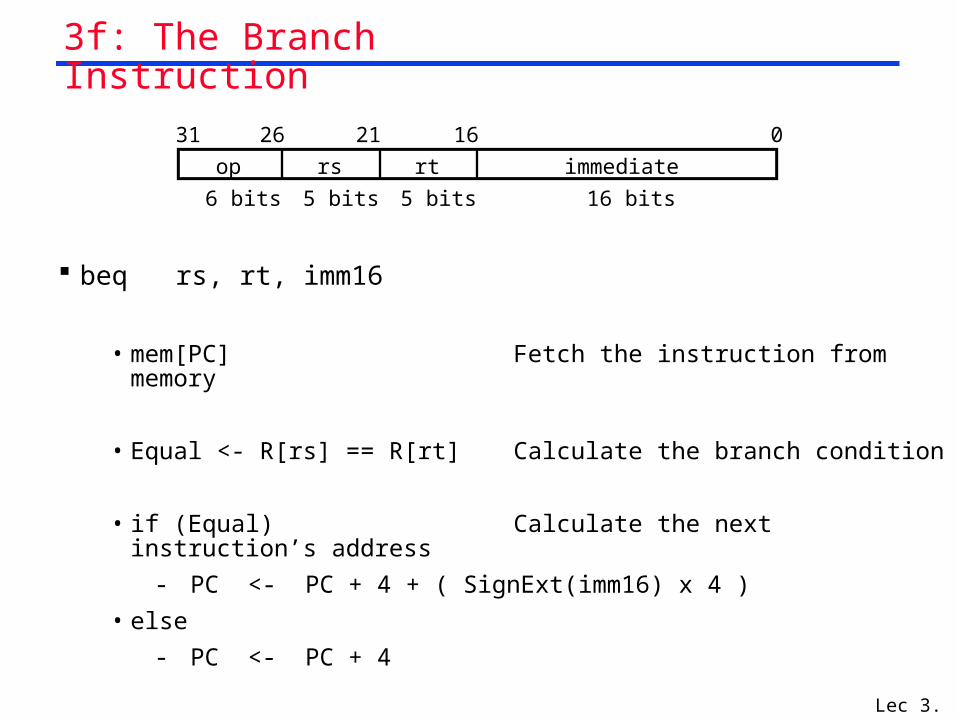
3f: The Branch Instruction
beq rs, rt, imm16
• mem[PC] Fetch the instruction from memory
• Equal <- R[rs] == R[rt] Calculate the branch condition
• if (Equal) Calculate the next instruction’s address
- PC <- PC + 4 + ( SignExt(imm16) x 4 )
• else
- PC <- PC + 4
op rs rt immediate
016212631
6 bits 16 bits5 bits5 bits

Lec 3.29
Datapath for Branch Operations
beq rs, rt, imm16 Datapath generates condition (equal)
op rs rt immediate
016212631
6 bits 16 bits5 bits5 bits
32
imm16P
C
Clk
00
Ad
der
Mu
x
Ad
der
4nPC_sel
Clk
busW
RegWr
32
busA
32busB
5 5 5
Rw Ra Rb32 32-bitRegisters
Rs Rt
Eq
ual?
Cond
PC
Ext
Inst Address

Lec 3.30
Putting it All Together: A Single Cycle Datapath
imm
16
32
ALUctr
Clk
busW
RegWr
32
32
busA
32busB
55 5
Rw Ra Rb32 32-bitRegisters
Rs
Rt
Rt
RdRegDst
Exte
nd
er
Mu
x
3216imm16
ALUSrcExtOp
Mu
x
MemtoReg
Clk
Data InWrEn32 Adr
DataMemory
MemWrA
LU
Equal
Instruction<31:0>
0
1
0
1
01
<2
1:2
5>
<1
6:2
0>
<1
1:1
5>
<0
:15
>
Imm16RdRtRs
=
Ad
der
Ad
der
PC
Clk
00
Mu
x
4
nPC_sel
PC
Ext
Adr
InstMemory

Lec 3.31
A Single Cycle Datapath
PC
Instructionmemory
Readaddress
Instruction[31– 0]
Instruction [20– 16]
Instruction [25– 21]
Add
Instruction [5– 0]
MemtoReg
ALUOp
MemWrite
RegWrite
MemRead
BranchRegDst
ALUSrc
Instruction [31– 26]
4
16 32Instruction [15– 0]
0
0Mux
0
1
Control
Add ALUresult
Mux
0
1
RegistersWriteregister
Writedata
Readdata 1
Readdata 2
Readregister 1
Readregister 2
Signextend
Shiftleft 2
Mux
1
ALUresult
Zero
Datamemory
Writedata
Readdata
Mux
1
Instruction [15– 11]
ALUcontrol
ALUAddress

Lec 3.32
An Abstract View of the Critical Path Register file and ideal memory:
• The CLK input is a factor ONLY during write operation
• During read operation, behave as combinational logic:
- Address valid => Output valid after “access time.”
Critical Path (Load Operation) = PC’s Clk-to-Q + Instruction Memory’s Access Time + Register File’s Access Time + ALU to Perform a 32-bit Add + Data Memory Access Time + Setup Time for Register File Write + Clock Skew
Clk
5
Rw Ra Rb
32 32-bitRegisters
RdA
LU
Clk
Data In
DataAddress
IdealData
Memory
Instruction
InstructionAddress
IdealInstruction
Memory
Clk
PC
5Rs
5Rt
16Imm
32
323232
A
B
Next
Ad
dre
ss

Lec 3.33
An Abstract View of the Implementation
DataOut
Clk
5
Rw Ra Rb
32 32-bitRegisters
Rd
ALU
Clk
Data In
DataAddress
IdealData
Memory
Instruction
InstructionAddress
IdealInstruction
Memory
Clk
PC
5Rs
5Rt
32
323232
A
B
Next
Ad
dre
ss
Control
Datapath
Control SignalsConditions

Lec 3.34
Steps 4 & 5: Implement the control
Next time

Lec 3.35
Summary 5 steps to design a processor
• 1. Analyze instruction set => datapath requirements
• 2. Select set of datapath components & establish clock methodology
• 3. Assemble datapath meeting the requirements
• 4. Analyze implementation of each instruction to determine setting of control points that effects the register transfer.
• 5. Assemble the control logic
MIPS makes it easier
• Instructions same size
• Source registers always in same place
• Immediates same size, location
• Operations always on registers/immediates
Single cycle datapath => CPI=1, CCT => long
Next time: implementing control