Embed Size (px)
Citation preview

EEE Links, Volume 9, No. 1, January 2003
Focus on Plastic Parts
TABLE OF CONTENTS
DEPARTMENTS
Letter From the Editor
Guidelines for EEE Links Article Submission
Upcoming Events
Programmable Logic Application Notes
FEATURE CONTENT
Plastic Encapsulated Microcircuits (PEMs) NEPP Web Site (Summary and Links)
Moisture Characteristics of Molding Compounds and Environmental Effects in PEMs (Abstracts/Conclusions)Alexander Teverovsky, QSS Group, Inc./NASA GSFC
Moisture Diffusion in Molding Compounds and Quality Assurance of PEMs for Space Applications (Abstract)Alexander Teverovsky, QSS Group, Inc./NASA GSFC
Qualification of PEMs Using Board-level Testing (Abstract)Alexander Teverovsky, QSS Group, Inc./NASA GSFC
A Technique for Assessing the Moisture Resistance of PEMs Using MOS Test Structures (Report)
Alexander Teverovsky, QSS Group, Inc./NASA GSFC
Evaluation of Data Retention and Imprint Characteristics of FRAMs Under Environmental Stresses for NASA Applications (Report)Ashok Sharma, NASA GSFC, and Alexander Teverovsky, QSS Group, Inc./NASA GSFC
Notes on the Reliability of HST Gyros (Abstract)Henning Leidecker, NASA GSFC, and Walter Thomas, NASA GSFC
Thermal Cycling Characterization of GaAs PHEMT Transistors and Test Structures (Abstract/Summary)Ashok K. Sharma, NASA GSFC, and Muzar A. Jah, NASA GSFC
Life-Cycle Forecasting, Mitigation Assessment, and Obsolescence Strategies (Summary)Michael Pecht, CALCE/UMD, Rajeev Solomon, CALCE/UMD, Peter Sandborn, CALCE/UMD, Chris Wilkinson, CALCE/UMD, and Diganta Das, CALCE/UMD
Radiation Evaluation Method of Commercial Off-the-Shelf (COTS) Electronic Printed Circuit Boards (PCBs) (Abstract)Kenneth A. LaBel, NASA GSFC, Paul W. Marshall, Consultant, Timothy D. Gruner, NASA GSFC, Robert A. Reed, NASA GSFC, Beverly Settles, NASA GSFC, Jonathan Wilmot, NASA GSFC, Lamar F. Dougherty, NASA GSFC, Angela Russo, NASA GSFC, Michele Gates Foster, NASA HQ, William Yuknis, NASA GSFC, and Ann Garrison-Darrin, NASA JPL/APL
1

Test Flows for Space PEMs (Abstract)Harry Shaw, NASA GSFC, Jeannette Plante, Dynamic Range, and Brandon G. Lee, Dynamic Range
Plastic Encapsulated Microcircuits (PEMs) Reliability/ Usage Guidelines for Space Applications (Summary)Michael Sandor, NASA JPL/California Institute of Technology
Creep Corrosion Over Plastic Encapsulated Microcircuit Package with Noble Metal Pre-plated Leadframe (Abstract)P. Zhao, CALCE/UMD, M. Pecht, CALCE/UMD, and C. Hillman, CALCE/UMD
Update on the Qualification of PEMs in Space (2002 MAPLD International Conference) (Abstract)Joseph J. Fabula, Xilinx Corporation
CALCE Technical Review and Planning Meeting Briefing (Summary)CALCE Electronic Products and Systems Center/University of Maryland
Excerpt From NEPP Fourth Quarter Status Summary Report on PEMs Task: Reliability of COTS PEMs, Packaging/PEMs Qualification Methods, Necessity for Upscreening, Guidelines Support (Summary)Ashok K. Sharma, NASA GSFC
Table of GSFC PEMs Evaluation Reports/Test Lab Report SummariesInvestigator: Chris Greenwell, QSS Group, Inc./NASA GSFC
First Call for Papers for 2003 MAPLD International Conference, Reagan International Trade Center, Washington,
DC, September 9-11, 2003 (Announcement Summary)Richard Katz, NASA GSFC
DEPARTMENTS
Letter From the Editor
Jeanne A. Beatty, EEE Links EditorQSS Group, Inc./NASA GSFC
Greenbelt, MD [email protected]
301.286.7878
Welcome to the January 2003 issue of EEE Links. The Programmable Logic Application Notes column has now been reinstated in this newsletter. Written by Rich Katz of NASA’s Office of Logic Design (OLD), the application notes offer technical tips intended to prevent flight design errors and enhance research, development, and use of programmable logic and elements for space flight applications. An archive of these notes columns from previous issues of EEE Links is available at http://www.klabs.org/richcontent/eeelinks/EEE_Links.htm.
The primary source of the application notes is Rich’s Web site at http://klabs.org. A new feature of the site, which contributed to this edition’s content, is the OLD News Web site at http://klabs.org/richcontent/old_news. See the column on page 7 below for information about joining the mailing list to receive the notes via e-mail.
Thanks to the many authors who contributed to this issue. Please send questions, suggestions, and comments about the newsletter and its topics to my e-mail address cited above, or contact me by telephone Monday through Friday between 8:30 a.m. and 5:30 p.m. EST.
2

DEPARTMENTS
Guidelines for EEE Links Article Submission
The next EEE Links publication date and focus will be:
June 2003 – NASA EEE Parts Assurance Group (NEPAG)Article submission deadline is May 15, 2003.
Submitting articles for EEE Links is a great means by which to transfer information and knowledge inside and outside of the NASA community.
EEE Links supports the NASA Electronic Parts and Packaging Program (NEPP), and the information presented in this newsletter augments electronic parts, packaging, and radiation technologies.
EEE Links publishes many types of articles relevant to electronic parts, packaging, and radiation. Primary consideration is given to articles that relate specifically to the NEPP program, but we also consider articles outside of the NEPP program that address electronic parts, packaging, or radiation issues.
Article submissions can cover current efforts, referencing status and completion date. Articles can be informal and be from one paragraph to three pages in length on the following subjects:
Current Events Within the NEPP Program and Projects
Parts Packaging
Radiation Reliability Issues Concerning
NEPP New/Emerging Technology Space Flight Hardware Quality Assurance Issues.
To submit an article, please send it in a text-only format, preferably Microsoft Word, to Jeanne Beatty at [email protected]. Please provide the following information with your article submission:
Abstract: This two- to four-sentence paragraph summarizes the key points to capture the reader’s attention.
Contact Information: The author must include his or her business address, phone, fax, and e-mail address.
Notes and References: Most articles require some references, and some contain incidental information best treated as notes. Use brackets for references and superscripts for notes, then list the two groups separately at the end of the article. These should be numbered in the order in which they appear in the article, not alphabetically.
Additional Reading: Our readers appreciate pointers to relevant books and articles. List these at the end of the article in the same format as the references.
Copyright: The author is responsible for obtaining any copyright releases or other releases necessary for their article. The releases should be forwarded to the EEE Links Editor (see Jeanne Beatty’s e-mail address above).
3

Biography (to be supplied when requested): This should be between 50 and 75 words outlining the author’s job, background, professional accomplishments, and other pertinent accolades or areas of interest. Accompanying photographs might be requested also; these should either be in .gif or .jpg format if possible.
Letters to the Editor
Please limit letters to 250 words. Include your name, phone number, and e-mail address. Names are withheld from publication upon request. We reserve the right to edit for style, length, and content.
DEPARTMENTS
Upcoming Events
Commercialization of Military and Space Electronics, 7th International CMSE ConferenceFebruary 10-13, 2003, Sheraton Gateway Hotel, Los Angeles, CAFor details, contact Dale Stamps or Leon Hamiter, [email protected] or [email protected], 256.536.1304, or see Web site www.cti-us.com
Sixth WASPP Program (Wafer Applied Seal for PEM Protection)February 13, 2003, Los Angeles Marriott Hotel, Los Angeles, CAFor details, contact Pete Black, [email protected], 256.876.3004, or see Web site http://www.waspp.org
Ground System Architectures WorkshopMarch 4-6, 2003, Manhattan Beach Marriott, Manhattan Beach, CAFor details, contact [email protected], or see Web site http://www.aero.org/conferences/gsaw
Radio Frequency Interface Forum 2003, RFI Issues in Space OperationsMarch 18-19, 2003, Intelsat Headquarters, Washington, DCFor details, contact [email protected], or see Web site http://www.aero.org/conferences/rfiforum
IMAPS Ceramics 2003, Ceramic Interconnect Technology: The Next GenerationApril 7-9, 2003, Westin Hotel, Denver, COFor details, contact Jackki Morris-Joyner, [email protected], 305.382.8433, or see Web site http://www.imaps.org/callfor/ceramic2003.htm
Fifth International Conference on Electronic Packaging Technology (ICEPT 2003), Second Call for PapersApril 21-22, 2003, Shanghai, ChinaFor details, contact Jackki Morris-Joyner, [email protected], 305.382.8433, or see Web site http://www.icept2003.org
Space Power Workshop 2003April 21-24, Crowne Plaza Redondo Beach, Redondo Beach, CAFor details, contact Jackie Amazaki, SPW Administrator, 310.336.4073, Alexander Rivera, General Chair, 310.336.0158, or Katy Feine, SPW Registrar, 310.336.6805, or see Web site http://www.aero.org/conferences/power/
4
Fourth Annual NEPP ConferenceApril 29 to May 1, 2003, Sheraton Cleveland Airport Hotel, Cleveland, OHFor details, contact Dory Josephson, [email protected], 301.286.7927m, or see Web site http://nepp.nasa.gov/index_nasa.cfm/770/
IMAPS ATW on PackagingMay 13-15, 2003, San Diego, CAFor details, contact Jackki Morris-Joyner, [email protected], 305.382.8433, or see Web site http://www.imaps.com
IMAPS Topical Workshop & Exhibition on Flip Chip TechnologiesJune 16-18, 2003 Four Seasons Hotel Austin, TXFor details, contact Jackki Morris-Joyner, [email protected], 305.382.8433, or see Web site [email protected]
14th European Microelectronics and Packaging Conference & ExhibitionJune 23-25, 2003, Friedrichshafen/Germany Lake Constance GrafZeppelinHausFor details, contact Mrs. Henny Brabec, [email protected], ++49 7621 98 33 33, or see Web site [email protected]
Sixth Annual Military and Aerospace Programmable Logic Devices (MAPLD) International ConferenceSeptember 9-11, 2003, Reagan International Trade Center, Washington, DCFor details, contact Richard Katz, [email protected], 301.286.9705, or see Web site http://klabs.org/mapld03
Aerospace Testing Seminar, Effective Testing in a Challenging Project EnvironmentOctober 21-23, 2003, Manhattan Beach Marriott, Manhattan Beach, CAFor details, contact [email protected], or see Web site http://www.aero.org/conferences/ats
5

Fourth Annual NEPP Workshop
April 29 – May 1, 2003
Sheraton Cleveland Airport Hotel - Cleveland, OH(Near Glenn Research Center)
Registration and Program: TBA - Check this page in the future
Program Point of Contact - Phil Zulueta: [email protected]
Phone: 818-354-1566 – Fax: 818-393-5245
Hotel Reservations:Room Rate For All Workshop Attendees is $86/night
Group Name: NASA NEPP WorkshopCoordinator: Dory Josephson : [email protected]
Phone: 301-286-7927 – Fax: 301-286-0301
Sheraton Cleveland Airport Hotel - 800-362-2244Space is limited - Reservations will be handled on a first come, first
served basis
6

DEPARTMENTS
Programmable Logic Application Notes
TRST* and the IEEE JTAG 1149.1 Interface
(Office of Logic Design News #7)
Richard KatzNASA GSFC
[email protected] 301.286.9705
Many modern digital devices have test circuitry built-in, compliant with the IEEE JTAG 1149.11 standard. It is critical that this interface remain disabled during flight operations. If enabled, complete loss of control of the device may occur and power cycling of the device may be required. Recent reviews of FPGAs and microprocessors have shown a number of instances in which this interface was not understood, particularly for spaceborne, high-reliability applications, and the devices were not configured properly.
The central point of the JTAG circuitry is the Test Access Port (TAP) controller, a finite state machine. This controls many device resources such as the command register, which in turn controls the I/O pins. One state in test mode is an “external test” in which all pins actively drive onto the board, with the levels controlled by a special shift register, whose contents are undefined. Other modes include turning all pins into input pins. This mode can override the user specification for an I/O module; an I/O module configured by the user as an input can drive as an output in test mode.
The disabled state for the TAP controller is called TEST-LOGIC-RESET. When the device is powered on, an internal circuit puts the TAP controller into this home state. During operation, it’s important to keep the TAP controller in this state, as the flip-flops comprising the TAP controller’s finite state machine can be upset from either radiation or electronic disturbance, both of which have happened in real circuits.
The 1149.1 specification has a TRST* (test reset, active low) pin that forces the TAP controller into the TEST-LOGIC-RESET state. This pin should be grounded on the printed circuit board and verified with an ohm meter, since it is difficult to determine the state of the connection by test. 1149.1 compliant devices have an internal pull-up resistor on the TRST* pin, so the pin should not be pulled down through a resistor; a hard ground should be used instead. Left unconnected, the TRST* pin will be asserted and the device will not be held in the TEST-LOGIC-RESET state.
There is one problem with the above paragraph: The TRST* pin is an option in 1149.1, and many devices used in spaceborne applications do not implement it. If these devices are used, circuits must be analyzed very carefully to ensure that no system-level ill effects can occur. In this case, ensure that two other pins in the 1149.1 interface are configured appropriately. First, the TCK (test clock) pin should be actively clocked by an independent clock signal. The system clock signal should not be used; if it is tied to a JTAG compliant device, the clock input might turn into an output and clamp the clock signal—deadlock. Second, ensure that the TMS (test mode select) pin is driven high.
7

Theoretically, under worst-case conditions, this will ensure that the TAP controller has returned to the TEST-LOGIC-RESET state in no more than five cycles of TCK. In practice, however, devices that have lost control sometimes require a power-on reset to restore the device to an operational mode.
Note: The full version of this article includes figures, captions, and links to the references for additional information. Go to http://klabs.org/richcontent/old_news/old_news_7/old_news_7.htm
References
1. The motivation for this specification is testing of connections on the printed circuit board. Many devices make other uses of this port for things such as electronic probing, programming, built-in-test, etc. The governing standard is “IEEE Std. 1149.1-1993, IEEE Standard Test Access Port, and Boundary-Scan Architecture,” IEEE, Inc., New York.
2. “Current Radiation Issues for Programmable Elements and Devices,” R. Katz, et al., IEEE Transactions on Nuclear Science, December 1998.
3. “Use of SX Series Devices and IEEE 1149.1 JTAG Circuitry,” R. Katz and J. J. Wang.
4. “TRST Pin for SX, SX-A, and SX-S Devices,” R. Katz and Actel.
A Note From the Author: In my new OLD (Office of Logic Design) position, I am now making some of my informal e-mail lists semi-formal. These mailings have pointers to technical tips that can [hopefully] proactively prevent errors from getting into flight designs, or make things go faster and smoother. The list includes an array of people from a number of organizations—different NASA Centers, the European Space Agency (ESA), etc.—and all are encouraged to share the mailings with colleagues. This list is targeted towards those that either will design or review space flight digital electronics. Feel free to suggest topics for discussion and research or to contribute news items. To become a recipient on this mailing list, please send e-mail to [email protected]. All Application Notes are uploaded onto my WWW site, and new additions are noted on the What’s New page; see URLs below:
OLD News Archive: http://klabs.org/richcontent/old_news What’s New: http://www.klabs.org/whats_new.htm
8

FEATURE CONTENT
Plastic Encapsulated Microcircuits (PEMs) NEPP
Web Site
http://nepp.nasa.gov/index_nasa.cfm/678
Background Information
PEMs offer advantages of size, weight, cost, and availability. The traditional barrier to their use in highly reliable systems has been their perceived lower reliability in space and aerospace applications. Refer to NASA Directive NPD 8730.2 for guidelines in managing Electrical, Electronic, and Electromechanical (EEE) parts.
In spite of this perception, the space and aerospace electronics industries have begun to reconsider the use of PEMs for the following reasons:
1. Improvements in reliability of PEMs, as evidenced by their use in the automotive industry.
2. Improved methods of accelerated testing and reliability prediction.
3. Awareness that factors other than part reliability are more important than previously thought.
4. Concerns that many hermetic part types may not be available for future designs of space systems.
Replacing military part numbers with their commercial counterparts cannot be done with high-reliability applications. The entire system of parts specifications, qualification, screening, and control needs to be modified to accommodate
the unique features of PEMs. The use of PEMs at High Altitudes is being developed by Dr. McCluskey at the Computer Aided Life Cycle Engineering (CALCE) Electronics Products and Systems Center.
Links
Technical discussion on this site provides descriptions of and links to information on PEM selection, uprating, procurement, GIDEP PEM database, project listing, outgassing, degradation, radiation, and qualification and screening. Also on the site are links to NASA GSFC PEMs policy, best practices for PEMs, PEM reports, documents regarding PEMs by Michael Sampson, and other PEMs links.
Moisture Characteristics of Molding Compounds and
Environmental Effects in PEMs
Alexander TeverovskyQSS Group, Inc./Goddard Operations
I. Characteristic Times of Moisture Diffusion and Bake-out Conditions for Plastic Encapsulated Parts
Abstract
Simple equations for calculation of the characteristic times of moisture diffusion in plastic packages of different shapes and sizes are suggested. It is shown that the moisture-prevention strategy can be developed and the adequate bake-out regimens for different situations can be calculated based on the temperature dependency of the moisture diffusion
9

coefficient, D(T), of encapsulating polymer materials.
In the available literature, moisture diffusion characteristics of molding compounds used in plastic encapsulated microcircuits (PEMs) have been analyzed and typical D(T) characteristics are calculated. The bake-out times calculated using averaged diffusion characteristics of molding compounds are in agreement with the JEDEC recommendations. Examples of calculations of bake-out regimens for parts allowing only low temperature treatment and for parts temporarily exposed to high humidity conditions are considered.
Conclusion
Simple equations have been suggested to calculate moisture diffusion characteristic times and bake-out regimens for plastic encapsulated devices of different sizes and shapes.
Analysis of moisture diffusion coefficients reported in the literature shows that different molding compounds have values of D varying approximately an order of magnitude. Considering variations in shape and size of different plastic encapsulated parts, the required bake-out times might vary more than 10 times even within the same size group of the parts. To develop an adequate moisture protection strategy for parts intended for space applications, D(T) characteristics of the molding compound should be measured for each lot of PEMs.
Comparison of the bake-out times, which had been calculated using average moisture diffusion characteristics (Do =
7.3510-6 m2/sec and U = 0.43 eV), and the regimens suggested by the existing JEDEC standards IPC/JEDEC J-STD-033, are in reasonable agreement. However, the suggested method in this work allows for estimations of adequate bake-out conditions and provides much more flexibility, enabling calculation of the regimens for a specific lot of parts depending on their history of exposure to moisture environments and possible temperature conditions.
Calculations of the bake-out conditions for parts that do not allow high temperature treatment are performed. Variations in moisture concentration and content in PEMs temporarily exposed to humid environments before burn-in testing have been analyzed.
II. A Rapid Technique for Moisture Diffusion Characterization of Molding Compounds in PEMs
Abstract
A non-isothermal technique for rapid characterization of moisture diffusion in molding compounds of plastic encapsulated microcircuits (PEMs) is suggested. The technique is based on measurements of the weight losses during heating in dry conditions of a polymer sample or plastic package pre-saturated with moisture. It allows calculation of the moisture diffusion coefficients and the activation energy of diffusion. The duration of this test does not exceed a few hours, and the necessary calculations can be performed easily in an MS Excel spreadsheet. The test can be performed directly on PEMs using a thermogravimetric analyzer (TGA) or a simple balance with 0.1 mg accuracy and a regular thermal chamber, which is capable of providing a linear
10

temperature increase, fast heating to a pre-set temperature, and cooling down to room temperature.
The results obtained by the non-isothermal desorption technique are shown to agree with the results of the diffusion coefficient measurements obtained by conventional isothermal sorption/desorption techniques.
The effect of lead frames on measurement results is discussed. It has been demonstrated that the probability of moisture leakage along the molding compound/lead frame interface can be estimated by comparing diffusion coefficients measured on the molding compound and on the plastic package.
Temperature dependencies of moisture diffusion coefficients of molding compounds used in different types of PEMs (QFP, DIP, and PLCC packages) manufactured by different vendors have been characterized.
Conclusion
A rapid technique for measurements of moisture diffusion coefficients and the activation energy of diffusion in polymer materials has been described. The technique allows in-situ measurements of D(T) characteristics of molding compounds in PEMs by measuring mass losses of the package in dry conditions while the temperature is increasing with time. The accuracy of the measurements is approximately 30%, and within the experimental errors the data obtained with the non-isothermal diffusion technique agree with the results of conventional measurements based on isothermal kinetics of moisture sorption.
The technique can be implemented using a thermo-gravimetric analyzer, which allows measurements of mass losses uninterruptedly during the temperature increase. For relatively thick samples (more than 2 mm) a regular programmable temperature chamber, which allows fast heating/cooling and linear temperature increase with time, can be used. In this case, the weighting can be performed periodically using a regular balance with an accuracy of 0.1 mg after fast cooling of the sample to room temperature.
For packages with delaminations at the molding compound-lead frame interface, the diffusion coefficient determined for the package is larger than the one determined for a polymer sample. It has been shown that the degree of delamination (φ) could be estimated by comparing Dp and DMC values.
Several types of PEMs have been tested using the non-isothermal desorption technique. The results show that the diffusion coefficient of moisture in molding compounds at room temperature varied from 2.410-9 cm2/s to 3.210-8 cm2/s. The activation energy of moisture diffusion was in the range from 0.32 eV to 0.5 eV.
III. Environmentally Induced Swelling and Shrinkage of Molding Compounds in PEMs
Abstract
This work analyzes swelling and shrinkage of plastic packages of PEMs caused by various environmental conditions. These conditions include moisture sorption during normal storage in laboratory conditions, accelerated environmental stress testing in humidity
11

chambers, bake-outs at 125 oC and 150 oC, and short-term high temperature exposure at temperatures above 200 oC simulating soldering processes. The volume deviations in molding compounds and plastic packages of microcircuits were measured using a simple hygrostatic weighting technique.
Several types of plastic encapsulated microcircuits (PEMs) and encapsulating materials have been evaluated. The coefficients of moisture expansion (CME) were found to depend on moisturizing conditions, increasing with temperature and relative humidity above 60% RH. Saturation with moisture at 85 oC/85% RH resulted in the CME varying for different molding compounds from 0.1 to 0.49. The extent of deformations caused by moisture removal (baking out) in the samples stored for a long time at normal conditions (T 22 oC, RH 50%) was comparable with the deformation caused by swelling in high humidity environments. Depending on the type of molding compound used, initial moisture content, and temperature of bake, baking of PEMs can result either in increase or in decrease of the volume of the package. Exposure to high temperatures causes significant reduction of the volume of plastic packages. Different physical mechanisms of environmental effects causing swelling and shrinkage of plastic packages in PEMs are discussed.
Conclusion
A simple, hygrostatic weighting technique has been suggested to assess deviations in volume of plastic packages caused by environmentally induced swelling and shrinkage of molding compounds in PEMs.
Measurements of 11 different types of plastic packages and 3 types of liquid epoxy encapsulants showed that the coefficient of moisture expansion varies from 0.1 to 0.49 when the samples are moisturized at 85 oC/85% RH conditions.
The coefficient of moisture expansion is not a constant, but depends on moisturizing and baking conditions increasing with the moisture uptake at RH > 60%. The efficiency of moisture to cause swelling has a trend to increase at low humidities and after high temperature bakes (at T > 200 oC).
All tested molding compounds manifested virtually linear sorption isotherm at 85 oC. However, the swelling isotherms had a sigmoidal shape, indicating higher swelling efficiency of water molecules absorbed at low humidity (<60 % RH).
Depending on moisture content in a plastic package, baking at relatively low temperatures (125 oC to 150 oC) might result in positive or negative variations in the volume of PEMs. Baking of samples with even relatively low moisture content at temperatures above 200 oC significantly reduces the volume of molding compounds.
Physical mechanisms of environmentally induced volume deviations in PEMs are discussed. The observed anomalies in moisture-induced swelling and moisture desorption caused shrinkage of plastic packages are attributed to a creep in epoxy resins, which occurs at baking temperatures.
Moisture sorption in PEMs at normal laboratory conditions (~22 oC and ~50%
12

RH) during ground phase integration period or moisture desorption in vacuum during space operations might cause significant (up to 0.35%) deviations in the volume of plastic packages. Similar deformations might affect characteristics of precision microcircuits and degrade performance of sensitive space instruments. Parametric sensitivity of PEMs intended for space applications due to environmentally induced swelling and shrinkage of molding compounds requires additional analysis.
The full report is posted on the NEPP Web site at http://nepp.nasa.gov/DocUploads/B9C0B2A1-4C69-4CB5-94863C560CBB0B19/Moisture%20Characteristics%203-part%20NEPP%20report.doc
Moisture Diffusion in Molding Compounds and Quality
Assurance of PEMs for Space Applications
Alexander Teverovsky,QSS Group, Inc./Goddard Operations
Moisture diffusion in molding compounds in PEMs might cause problems during the ground phase period of integration and testing of flight hardware. Highly accelerated stress testing (HAST) is widely used to assure robustness of PEMs in moisture environments. This testing often results in failures due to extremely harsh environments, which are not only inadequate for space conditions, but are also much more severe than typical
conditions during the ground phase period.
In this work an approach to the moisture prevention strategy and adequate accelerated testing is suggested. The moisture prevention strategy can be implemented by reinforcement of the requirements for handling and storage of PEMs and PEM-containing assemblies, virtual evaluation of moisture content during storage and testing of the parts and assemblies, and calculations of the bake-out conditions.JEDEC recommendations for bake-out conditions, accelerated factors of standard HAST testing, and the relevance of HAST conditions to typical ground phase environment have been analyzed. A possible alternative to HAST to assure quality of PEMs for space applications is discussed.
A simple method for in-situ measurements of temperature dependence of moisture diffusion characteristics of MC in PEMs is described. Results of these measurements can be used to calculate moisture distribution in plastic packages, estimate bake-out conditions, and develop an adequate accelerated stress testing.
This report is under review and will be posted on the NEPP Web site when complete.
13

Qualification of PEMs Using Board-level Testing
Alexander TeverovskyQSS Group, Inc./Goddard Operations
Abstract
This paper describes low-cost alternatives to the product assurance system for Plastic Encapsulated Microcircuits (PEMs) described in the 311-INST-001 instructions, Revision A, PEMs section, June 2002 (referred to hereafter as 311-PEM). It might be applicable to projects working under extreme time and budget constraints and willing to accept a higher level of risk on their parts program activities (typically level 3+ projects).
The suggested qualification system is based on board-level functional testing of the parts and includes several standard elements of the qualification system, such as destructive physical analysis (DPA), special design evaluation, and innovative qualification methods. An example of such a new method, monitored temperature transients, which is based on the local heating technique, is described.
The full report is available on the NEPP Web site at http://nepp.nasa.gov/DocUploads/22B45B90-F990-4360-A4485DD65CBD9510/Qualification%20System%20for%20PEMs%20Using%20Board-level%20Testing.doc
A Technique for Assessing the Moisture Resistance of PEMs Using MOS Test Structures
Alexander TeverovskyQSS Group, Inc./Goddard Operations
Abstract
A new technique for assessing the moisture resistance of PEMs is based on measurements of time-varying capacitance of a MOS structure with a large perimeter-to-area ratio of the metal electrode. When an inversion voltage is applied, the capacitance of the structure will increase with time due to lateral charge spreading. The rate of the charge redistribution and the magnitude of the change in capacitance depend on the moisture content on the die surface, and on some special features of the molding compound depend on die interaction. These conditions can be characterized by measuring the specific resistivity of the die-molding compound interface, s. The C(t) technique extends the limit of s measurements up to 1021 ohms. Experiments with different encapsulating materials proved the effectiveness of this technique for packaging evaluations. A good correlation between s and median time-to-corrosion failures was shown.
Introduction
Due to moisture permeability of polymeric materials, PEMs always have a certain moisture content on the die surface. The mechanisms of PEMs’ degradation due to moisture absorption (such as corrosion, leakage current, charge instability, etc.) strongly depend on the quality of the die-package
14

interface and its ability to prevent excessive moisture adsorption. Debonding between molding compound and die is considered as a major reliability concern for PEMs used in surface mount applications. Different types of comb pattern sensors have been commonly used since the 1970s to measure the surface specific resistivity, S, of oxide films and to find its relation to corrosion processes [1-3]. Use of this technique for PEMs is hindered due to the surface conductivity of the package and the volume conductivity of a molding compound that contains moisture. Normally, leakage currents in plastic packages would not exceed 10-12 A at 10 V, but in some cases these can be much higher [4]. Typically, during S
measurements, a low current sensitivity is 10-12 A, an equivalent pattern size is 10 m of width and 100 mm of length, and an applied voltage does not exceed 100 V. With these parameters, the technique is limited to a maximum sensitivity of 1018 ohms for S. A low frequency capacitance measurement technique developed by Merrett, Sim, and Bryan [5] is capable of being used directly with some types of microcircuits but is limited to a sensitivity of 1014 ohms. Besides, changes in the frequency dependence of the dielectric permittivity of the molding compound (and changes in the capacitance between the package leads) during humid testing may introduce errors in the calculation of S.
Moisture resistance and reliability of PEMs have been significantly increased over the last decade. The current trend is toward use of PEMs in highly reliable applications (military and aerospace) and in a harsh environments. New packaging systems require a more sensitive technique for assessing
moisture resistance. A new technique, described in this article, is based on a lateral charge spreading phenomenon and employs a metal-oxide-silicon (MOS) structure with a large perimeter-to-area ratio. The charge spreading process had been well known since 70th [6] and was one of the major cause of excessive leakage currents and failures of the first semiconductor devices and microcircuits encapsulated in polymers.
When an inversion voltage is applied to a MOS structure, the capacitance will increase with time due to a lateral spreading of the inversion layer area. The rate of this process depends on the rate of charging of the distributed oxide capacitance and is controlled by the surface resistivity. This allows one to calculate s using C(t) measurements. The technique uses integration of the surface current on the distributed oxide capacitance, which allows extending the limit of s measurements to 1021 ohms. Experiments with different encapsulating materials proved the effectiveness of the technique for packaging quality evaluation. A good correlation between s and median time to corrosion failure was shown.
Technique
Let us consider a MOS structure that is formed on n-type silicon with a strip metal electrode of the width d (see Figure 1).
15

Figure 1. MOS structure with a strip metal electrode.
A second electrode on the oxide surface is placed equidistantly at both sides from the first at a distance l and is connected to the substrate. Capacitance of this structure as a function of applied voltage (C-V characteristic) is shown in Figure 2. Let V0 be a negative voltage that is applied to the first electrode. V0<Vi, whereVi is the potential that causes formation of an inversion layer. Due to some conductivity of the oxide surface, the oxide areas around the first electrode will charge with time to a potential V(x,t). When -V(x,t) > -Vi, the depletion and inversion layers expand, thus resulting in an increase in capacitance (see Figure 3).
Figure 2. MOS-capacitance diagram (a) and capacitance variation with voltage (b). The flat
band capacitance Cfb and the corresponding voltage Vfb used in C-V technique to calculate the value of the oxide charge can be used to
calculate the inversion voltage Vi.
Figure 3. MOS capacitance after charge spreading.
Potential distribution along the surface of the MOS structure, V(x,t), can be calculated with the help of an equivalent diagram (see Figure 4) that is represented as an R-C-G chain, where R is the surface resistance, C is the capacitance of the oxide film, and G is the volumetric conductivity of the oxide. Normally, oxide films have very low volumetric conductivities and can be neglected. Therefore, the potential distribution can be described by a simple telegraph equation:
,
(1)
where C00 is the specific (per unit
area) capacitance of the oxide.
Figure 4. Equivalent diagram of a MOS-structure.
16
Using dimensionless coordinates: ,
, and , where
, equation (1) can be
simplified as follows:
(2)
The initial and boundary conditions are:
u(,0) = 0 at 0 < < l
u(0, ) = 1
u(1, ) = 0 (3)
The solution for (2), (3) is:
(4)
Figure 5 shows potential distributions calculated at different . At 3, a steady-state condition exists and is the characteristic time of this process. Using the plot in Figure 5, the dependence of the inversion area size on time, Xi(t), can be obtained from the following equation:
(5)
Figure 5. Calculated potential distribution along the surface of an MOS-structure.
An increase in inversion area, Xi, results in an increase in the capacitance of the MOS structure, C. In the frequency range of 100 Hz to 100 KHz, the resistance of the inversion layer is negligible compared with the capacitance impedance [7]. In this case, the capacitance will depend only on the size of the inversion area:
(6)
where is the
capacitance of the depletion layer.
This equation allows one to calculate the size of the inversion area using the capacitance measurements:
(7)
where C=C-Ci (see Figure 3).
The MOS capacitance parameters, C0 and Ci, as well as the potential of
17

inversion Vi, can be found from the initial C-V characteristic (see Figure 2) or from measurements of an additional MOS capacitance structure with a low perimeter-to-area ratio.
Using the plot of u(,), which is shown in Figure 5, and the size of inversion area, Xi , which may be calculated using Eq.(7), one can then determine the corresponding rated time, , and calculate the surface resistivity as follows:
(8)
To illustrate, Figure 6 displays the relationship of s and C for different values of ui, where ui = Vi/V0. Calculations have been made for a MOS structure consisting of n-type of silicon with 20 ohm-cm resistivity and an 1100 Å film of thermally grown oxide. This MOS structure featured the following parameters: d = 10 m, l = 60 m, C0 = 100 pF, Ci = 17 pF, Vi = -1.5 V. The measurement time, t, was 10 minutes.
Figure 6. Surface resistivity-capacitance relationship as a function of the rated inversion
potential ui.
As can be seen, capacitance changes of several tenths of picofarads correspond
to a s of more than 1020 ohms. Similar changes can be reliably measured using a digital R-C-L bridge. When applied to MOS structures with larger perimeter-to-area ratios and thinner oxides, the sensitivity of this technique can be increased to more than 1021 ohms. A software routine has been developed which allows calculation of the specific resistivity of a silicon oxide-molding compound interface using the above-described capacitance variance measurements. It allows calculation of s for any measurement time and for MOS structures with various dimentional and electrical parameters.
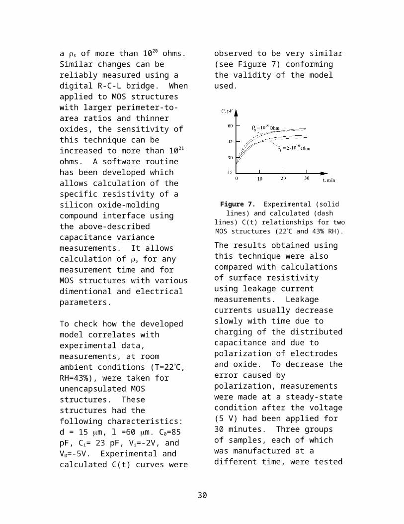
To check how the developed model correlates with experimental data, measurements, at room ambient conditions (T=22C, RH=43%), were taken for unencapsulated MOS structures. These structures had the following characteristics: d = 15 m, l =60 m. C0=85 pF, Ci= 23 pF, Vi=-2V, and V0=-5V. Experimental and calculated C(t) curves were observed to be very similar (see Figure 7) conforming the validity of the model used.
Figure 7. Experimental (solid lines) and calculated (dash lines) C(t) relationships for two
MOS structures (22C and 43% RH).
The results obtained using this technique were also compared with calculations of
18

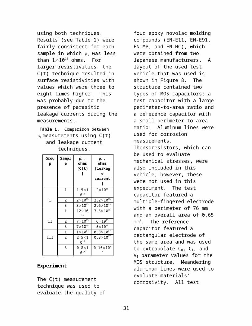
surface resistivity using leakage current measurements. Leakage currents usually decrease slowly with time due to charging of the distributed capacitance and due to polarization of electrodes and oxide. To decrease the error caused by polarization, measurements were made at a steady-state condition after the voltage (5 V) had been applied for 30 minutes. Three groups of samples, each of which was manufactured at a different time, were tested using both techniques. Results (see Table 1) were fairly consistent for each sample in which s was less than 11016 ohms. For larger resistivities, the C(t) technique resulted in surface resistivities with values which were three to eight times higher. This was probably due to the presence of parasitic leakage currents during the measurements.
Table 1. Comparison between s
measurements using C(t) and leakage current techniques.
Group Sample s , ohms[C(t)]
s , ohms[leakage current]
1 1.5101
521015
I 2 21015 2.21015
3 31015 2.61015
1 121015 7.51015
II 2 71015 61015
3 71015 51015
1 11017 0.31017
III 2 2.5101
70.31017
3 0.8101
70.151017
Experiment
The C(t) measurement technique was used to evaluate the quality of four epoxy novolac molding compounds (EN-E11, EN-E91, EN-MP, and EN-HC), which were obtained from two Japanese manufacturers. A layout of the used test vehicle that was used is shown
in Figure 8. The structure contained two types of MOS capacitors: a test capacitor with a large perimeter-to-area ratio and a reference capacitor with a small perimeter-to-area ratio. Aluminum lines were used for corrosion measurements. Thensoresistors, which can be used to evaluate mechanical stresses, were also included in this vehicle; however, these were not used in this experiment. The test capacitor featured a multiple-fingered electrode with a perimeter of 76 mm and an overall area of 0.65 mm2. The reference capacitor featured a rectangular electrode of the same area and was used to extrapolate C0, Ci, and Vi parameter values for the MOS structure. Meandering aluminum lines were used to evaluate materials’ corrosivity. All test vehicles were encapsulated in 16-lead DIP packages.
Ten samples with each type of encapsulating material were subjected to pressure cooker testing (PCT) at 121 C and 100% RH. Additionally, the samples encapsulated with EN-H were stored at 100% RH and at temperatures of 20 C, 85 C, and 100 C to check temperature effects on the interface resistivities. Periodically, the resistances of the aluminum lines and s values (using C(t) technique) were measured at room temperature. Resistance changes of more than 10% in the aluminum lines were considered to be failures. Resistance to corrosion was evaluated by calculating the median time to corrosion failures using log-normal plots.
19

Figure 8. Test structure layout. 1 – MOS capacitance structure with large perimeter-
to-area ratio; 19 – equidistant electrode connected to the substrate (5); 20 – a
reference MOS capacitor; 6-16, 10-18, and 11-17 – aluminum lines; 2-3-4, 7-8-9, and 12-13-14-15 – groups of thensoresistors (were not used during the experiment).
Figure 9 shows the time dependence of the interface resistivity during humidity aging at different temperatures. At all temperatures, s initially remains high, but then drops approximately five to six orders of magnitude. The approximate times, r, until s drops dramatically, are shown in Table 2. Calculated times, d, which are required for moisture to diffuse to the die surface, are also displayed. d =4L2/2D where D is the diffusion coefficient and L is the molding compound thickness above the die. As shown, r and d are in reasonably good agreement, suggesting that no moisture penetration along the lead-encapsulating material intrerface occurred.
Figure 9. Effect of temperature on the interface resistivity during humidity aging at 100% RH.
Table 2. Comparison of the times r and d (hours) for 16-lead DIP
packages.
Parameter Temperature, C
20 85 100 120r 10,000 400 120 50d 4500 350 95 35
Figure 10 shows changes in the interface resistivities obtained for different encapsulating materials during PCT. All encapsulating materials initially exhibited similar and high (>51019 ohms) values of s which then dropped after approximately 35-70 hours. This suggests that all materials had similar diffusivity coefficients. However, the interface resistivities of these materials, under steady-state conditions, differed by approximately three orders of value. This indicates essential differences in conditions at the die-molding compound interfaces and results in significant differences in the corrosion resistance of aluminum metallization.
Figure 11 shows the correlation between the median time to corrosion failures 50
and the interface resistivities for those
20

materials mentioned above, together with some other materials that were investigated using the same technique.
Figure 10. Effect of molding compound on the interface resistivity.
Figure 11. Median life for aluminum corrosion vs. interface resistivity during
PCT at 121 C and 100% RH.
Conclusion
A C(t) technique for measuring the specific resistivity of die-molding compound interfaces has been described. This technique utilizes an MOS capacitance structure with a large perimeter-to-area ratio as a sensor and is based on the lateral spread charging phenomenon.
A simple R-C equivalent circuit has been shown to be adequate to describe this lateral charge spreading phenomenon
and the associated capacitance changes in the MOS structure. Calculations and experiments have shown that the technique allows calculation of specific resistivities up to 1021 ohms.
Different types of molding compounds exhibited similar times (35-70 hours) for moisture to penetrate to the die surface during PCT at 121 C/100% RH. However, these molding compounds exhibited die-molding compound interfaces with different specific resistivities s (41014 ohms to 21017 ohms). The results of s calculations correlated well with the median lifetime of aluminum corrosion.
References
1. K. Tsubosaki, Y. Wakashima, and N. Nagasima, Rate-determining factor of aluminum corrosion and a rapid method of assessing the moisture resistance of plastic encapsulated LSI, 21st Ann. Proc. Reliab. Phys., pp. 83 - 89, 1983.
2. R. B. Comizzoli, L. K.White, W. Kern, G. L. Schnable, D. A.Peters, C. E. Tracy, and R. D. Vibronek, Corrosion of aluminum IC metallization with defective surface passivation layer, 18st Ann. Proc. Reliab. Phys., pp. 282 - 292, 1980.
3. S. P. Sim and R. W. Lawson, The influence of plastic encapsulants and passivation layers on the corrosion of thin aluminum films subjected to humidity stress, 17st Ann. Proc. Reliab. Phys., pp. 103 - 112, 1979.
4. A. Teverovsky, Degradation of encapsulating materials and plastic packages for microcircuits
21

under moisture environments, 6th International Workshop on Moisture in Microelectronics, NIST, 1996.
5. R. P. Merrett, J. P. Bryant, and R. Studd, An appraisal of high temperature humidity stress tests for assessing plastic encapsulated semiconductor components, 21st Ann. Proc. Reliab. Phys., pp. 71 - 82, 1983.
6. E. R. Schlegel, G. L. Schnable, and R. F. Schwarz, Behaviour of surface ions on semiconductor devices, IEEE Trans. on ED, v. ED-15, N12, p.973, 1968.
7. A. Teverovsky, B. Omarov, and T. Volkova, Frequency dependence of the inversion layer channels in MOS-structures, Electrical Relaxation in Microcircuits, pp. 30-34, MIEM, Moscow, 1988.
This report is available on the NEPP Web site at http://nepp.nasa.gov/DocUploads/5FD09ABF-2394-4DC1-BA24CDD060AC6A90/TECHNIQUE.DOC
Evaluation of Data Retention and Imprint Characteristics of FRAMs Under Environmental Stresses for NASA Applications
Ashok K. Sharma, NASA [email protected]
Alexander Teverovsky, QSS Group, Inc./Goddard Operations
Terry W. Dowdy/NAVSEA CraneBrett Hamilton/NAVSEA Crane
Abstract
A major reliability issue for all advanced nonvolatile memory (NVM) technology devices including FRAMs is the data retention characteristics over an extended period of time, under environmental stresses and exposure to total ionizing dose (TID) radiation effects. For this testing, 256 Kb FRAMs in 28-pin plastic DIPs, rated for industrial grade temperature range of -40 C to +85 C, were procured. These are two-transistor, two-capacitor (2T-2C) design FRAMs. In addition to data retention characteristics, the parts were also evaluated for imprint failures, which are defined as the failure of cells to change states (e.g., from 1 to 0, or 0 to 1). These 256 K FRAMs were subjected to scanning acoustic microscopy (C-SAM); 1,000 temperature cycles from -65 C to +150 C; high temperature aging at 150 C, 175 C, and 200 C for 1,000 hours; highly accelerated stress test (HAST) for 500 hours; 1,000 hours of operational life test at 125 C; and total ionizing dose radiation testing. As a preconditioning, 10 K read/write cycles were performed on all devices. Interim electrical measurements were performed throughout this characterization, including special imprint testing and final electrical testing. Some failures were observed during high temperature aging test at 200 C, during HAST testing, and during 1,000 hours of operational life at 125 C. The parts passed 10 Krad exposure, but began showing power supply current increases during the dose increment from 10 Krad to 30 Krad, and at 40 Krad severe data retention and parametric failures were observed. Failures from various environmental group testing are currently being analyzed.
Introduction
22

Ferroelectric random access memories (FRAMs) are very attractive for space applications because of their nonvolatile characteristics, low power consumption, high operational speeds, and read/write cycling endurance specifications in tens of billions. FRAMs have two orders of magnitude less write access time and require three orders of magnitude less energy per bit write compared to conventional nonvolatile memory devices (EEPROMs and/or Flash Memory). FRAMs density has also improved significantly over the last few years, driven by a variety of commercial applications. The first 4 KB commercially available FRAMs were manufactured by Ramtron less than 10 years ago, and now memory densities of 1 Gb based on 0.18 m technology appear to be technically feasible [1].
An area of high interest in NVMs has been the development of thin-film FE technology to build FRAMs. However, these FE films used as memory storage elements have significant reliability concerns such as aging/fatigue effects from a large number of polarization reversal cycles, thermal stability, effects of electric field, and time dependent dielectric breakdown (TDDB) [2].
One of the major reliability issues for all nonvolatile memory devices, FRAM included, is data retention, which is defined as the ability of a memory device to maintain stored data between the time of writing and subsequent reading of the stored information. Temperature significantly accelerates retention failures due to thermal depolarization of the poled state in the ferroelectric material and is commonly used to accelerate this failure mechanism. Evaluation of low density
Ramtron FRAMs has demonstrated a failure rate of less than 60 fits with a 60% confidence level for 10-year data storage at room temperature [3]. However, data retention characteristics depend on manufacturing processes as well as design factors and remain a major reliability concern for new generations of FRAM microcircuits.
Another degradation mechanism, which is known to affect reliability of ferroelectric memories, is fatigue. Fatigue in ferroelectric materials is a decrease of switchable polarization with an increased number of switching cycles or polarization reversals. This degradation process is related to the electrode interfacial areas of the memory cells and can be significantly decreased by using appropriate electrode materials, for example RuO2/PZT structures, instead of Pt/PZT structures [4]. The electric-field-assisted migration of charged species (most likely oxygen vacancies) within ferroelectric materials may be also responsible for the degradation/fatigue behavior [5], [6].
In addition to retention and fatigue failures, other failure modes and mechanisms such as aging, imprint, and reducing environment degradation are known to be specific to ferroelectric memory cells in microcircuits. Aging is defined as a mechanism that causes signal loss during a retention period, which does not recover after a rewrite and immediate read. This differentiates it from the retention failures, where a signal recovers after rewrite and immediate read. Aging is considered as a gradual stabilization of the domain structure due to which the ferroelectric becomes less responsive to applied fields [7], [8]. Imprint is a phenomenon
23

specific to the ferroelectric materials. Once a capacitor has spent significant time in one polarity, it is reluctant to switch polarities [9]. This effect is due to accumulation of charges with time in the ferroelectric cell, which compensates the created polarization.
Annealing of Pt/PZT system in a hydrogen-containing ambient (e.g., forming gas) might cause severe degradation of PZT thin film [10]. Hydrogen that reaches the platinum-PZT interface is a strong enough reducing agent, with Pt as a catalyst, to take oxygen from the lead lattice of the PZT. This results in forming a water molecule, which reduces the adhesion between the PZT and platinum and degrades the signal from the ferroelectric cell. It was shown [11] that the hydrogen evolved from plastic packaging during molding, and post-mold cure can affect data retention reliability of FRAMs. Another mechanism of polarization suppression in PZT films is related to high temperature reducing treatments in dry nitrogen at 400 C [12]. This treatment creates oxygen vacancies, which might lock domains. The trapped charges are believed to inhibit the domain motion and cause failures of memory cells.
Although ferroelectric films have shown high radiation tolerance, results of total dose radiation testing of commercial FRAMs have shown these devices to be failing at 10 Krad and higher TID. Also, these FRAMs can typically latch up under relatively low energy heavy ion exposure. This is primarily due to radiation softness of underlying commercial processes used to fabricate these memories. For this evaluation, only TID testing was performed.
Ferroelectric memory is a relatively new, emerging technology, which requires in-depth understanding of the related reliability issues and extensive testing at extreme conditions for space applications. The objective of this work was to evaluate reliability of commercial 256 Kb FRAMs over a wide temperature range with a focus on data retention and imprint characteristics.
Background
In the NVMTS 2001, data retention and fatigue characteristics were reported of 64 Kb PZT-based FRAMs, tested over a temperature range from -85 C to +310 C for ceramic packaged parts and from -85 C to +175 C for plastic parts, during retention periods of up to several thousand hours. The observed data retention failures were divided into three categories: (1) random failures that were not related to stress conditions, (2) weak cell failures, which were also not related to a particular stress condition but were reproducible from test to test, and (3) intrinsic failures that were caused by thermal degradation (or wearout) of the ferroelectric cell material. A conclusion was that additional testing should be performed on higher density 256 Kb FRAMs.
Test Plan
24

For this testing, 256 Kb FRAMs in 28-pin plastic DIPs, rated for industrial grade temperature range of -40 C to +85 C, were procured. These are two-transistor, two-capacitor (2T-2C) design FRAMs. In addition to data retention characteristics, the parts were also evaluated for imprint failures, which are defined as the failure of cells to change states (e.g., from 1 to 0, or 0 to 1) and are somewhat similar to the hysteresis effect. Figure 1a shows a 256 Kb FRAM X-ray (top view), and Figure 1b shows an optical photograph of the die. Figure 2 shows a test flow chart for the environmental and electrical characterization testing, including radiation testing performed.
Figure (1a). 256 Kb FRAM (top view).
Figure (1b). Optical photograph of die.
Figure 2. Test flow chart.
Notes:
1. Two devices were sent for Construction Analysis (CA) before environmental testing. All devices were sent for C-SAM before and after tests.
2. Full electrical testing included input and output voltages and leakage currents, stand-by and active power supply currents, and chip enable access time. W/R0, W/R1, W/R CB, W/R Inverted CB, and W/R Random were included in a full Write/Read.
3. Temperature cycling was at temperatures -65 °C to 150 °C with 15 minute dwell at each extreme and 10, 40, 50, and 100 cycles, up to 1,000 cycles total. The total transfer time from hot to cold did not exceed 1 minute.
4. HAST was unbiased with five 100 hour test segments.
5. High Temperature Operating Life (HTOL) was dynamic. Electrical endpoints were at 250, 500 and 1000 hours.
6. For the temperature exposure test, lots were divided for three temperatures: 150 °C, 175 °C, and 200 °C. Electrical endpoints were at 100, 500, and 1,000 hours.
7. Total Dose Radiation Testing was performed in test segments at 1K, 3K, 5K, 10K, 20K, and 30K.
8. For each environmental step, a special test to detect imprint failures recommended by the manufacturer was performed. The test consisted of write pattern, bake-out at 70 C for 15 minutes, and read/verify pattern
25

during each interim and final electrical measurements.
Environmental and Radiation Testing
Visual/Serialization
All 97 devices were visually inspected, serialized, and sent to C-mode Scanning AcousticMicroscopy (C-SAM). All devices passed visual inspection and C-SAM.
Preconditioning
Ninety-five devices were given 10,000 Read/Write cycles prior to environmental tests.
Electrical Testing
Parametric measurements of I/O voltages, leakage currents (VOL, VOH, VIL, VIH, ILI, ILO), and Clock Enable Access time were made after every test increment. All electrical tests were performed at 25 °C. Retention tests (W/RO, W/R1, CB, Inverted CB, and W/R Random) were performed after every test increment. The devices were then baked at 70 °C for 15 minutes and the electrical and retention tests were repeated.
Temperature Cycling
Serial numbers 1-20 were tested as per MIL-STD-883, Method 1010, condition B (except the cold temperature was at -65 °C) for 1,000 cycles. Electrical tests were performed after every 100 cycles. Test lot did not experience any failures.
Highly Accelerated Stress Test (HAST)
This test was performed on S/Ns 21-40 with 500 hours of 130 °C at 85% RH at 2 atm in 100-hour intervals. S/Ns 31 and 37 experienced hard electrical failures after 400 hours. Multiple devices had memory read failures during the 500 hours of HAST, but were able to be rewritten.
High Temperature Operating Life (HTOL)
This test was performed on serial numbers 41-60 for 1,000 hours with endpoints taken at 250, 500, and 1,000 hours. The voltage level was set at 5.5 V at 125 °C. S/N 46 failed read 1 and CB after 500 hours. Other devices failed various memory reads, but were able to be rewritten.
High Temperature Exposure Aging
Twenty-four devices (S/Ns 61-84) were exposed to accelerated temperature aging at 150 °C, 175 °C, and 200 °C. Eight devices were exposed to each temperature. Electrical endpoints were taken at 250 hrs., 500 hrs., and 1,000 hrs. Testing was stopped after failures were noted at the 200 °C temperature after 500 hours of exposure. No failures occurred at 150 °C and 175 °C.
Total Dose Radiation Test
For radiation testing, Gamma Cell 220 was used at a dose rate of 83.3 rad/sec. A total of six devices in the test lot were irradiated under static bias, and one device was used as a control sample. HP82000 Automatic Test Equipment (ATE) was used for all the required functional and power supply tests that included random read, active current, standby current, input leakage current,
26

VOL, VOH, Clock Enable Access time, 0 pattern write, 1 pattern write, checkerboard write, and random write tests.
All devices remained functional through 10 Krad but began showing power supply current increases during the dose increment from 10 Krad to 30 Krad (see Table 2). In the post 30 Krad electrical test, all parts showed increased power supply currents (combined currents rising from 1.24 ma to 0.263 A during irradiation) and one part (S/N 90) showed complete electrical and data retention failure. After 40 Krad, the remaining five test parts showed severe data retention and parametric failure as evidenced by electrical test failure (S/Ns 86, 88, and 89). Serial number 85 failed the random read test. Annealing for one day (room temperature anneal with bias applied and 70 °C heated anneal without bias) showed a small amount of parametric recovery, but the power supply parametric and data retention failures remained.
Table 1 provides a summary of environmental and electrical characterization including radiation test results.
Table 1. Environmental, electrical, and radiation test results summary.
Test Test Condition
Qty. Tested
Failed Remarks
Temp. Cycling
1,000 cycles -65 °C to 150 °C
20 0
HAST130 °C, 85% RH, 500 hrs., 2 atm
20 2S/Ns 31 & 37 failed various electrical endpoints at 400 hours and were not able to be reprogrammed. Other devices
had memory read failures after HAST but were able to be reprogrammed.
HTOL 1,000 hrs. at 125°C
20 1S/N 46 failed read 1 and CB after 500 hours and could not be reprogrammed. Other devices failed various memory reads, but were able to be reprogrammed.
150 °C Temp. Exp.
1,000 hrs. 8 0
175 °C Temp. Exp.
1,000 hrs. 8 0
200 °C Temp. Exp.
1,000 hrs. 8 8All eight devices passed electrical endpoints after 100 hours but failed various electrical endpoints after 500 hours. Testing was stopped after 500 hours.
Total Dose Rad.
6 6 Devices passed exposures through 20 Krads but failed after 30 Krads.
Data Retention and Imprint Test Summary
Temperature cycling can potentially degrade the retention characteristics of FRAMs. However, temperature cycling performed on 20 FRAM sample devices for 1,000 cycles as per test conditions shown in Figure 2 test flow showed no data retention or imprint failures.
HAST was performed on 20 FRAM sample devices as per Figure 2 test flow. Test results showed multiple devices failing post HAST interim and final electrical measurement read test but were able to be reprogrammed,
27

indicating data retention failures. Two devices experienced hard failures after 400 hours of HAST testing. HTOL test was performed on 20 FRAM sample devices that were subjected to 1,000 hours life test at 125 °C as per Figure 2 test flow. Test results showed multiple devices failing interim and final post HTOL electrical measurements read test but were able to be reprogrammed, indicating data retention failures. One device was a hard failure and could not be reprogrammed. No imprint test failures were observed during HAST or HTOL testing. Two HAST failures and one HTOL failure are undergoing analysis including C-SAM inspection. Twenty-four devices were subjected to high temperature exposure aging at 150 °C, 175 °C, and 200 °C. Eight devices were exposed to each temperature. Electrical endpoints were taken at 250 hrs., 500 hrs., and 1,000 hrs. No failures occurred at 150 °C and 175 °C. Testing was stopped after failures were observed at the 200 °C temperature after 500 hours of exposure, and these failures could not be reprogrammed. Some of these failures are being subjected to additional analysis. Table 2 shows high temperature exposure aging test summary, and Figure 3 shows the time versus % of failed vectors for three temperatures testing.
Table 2. High temperature exposure aging test summary.
Total Retention 150 °C 175 °CTime Test Failed Failed Failed Failed Failed(hrs.) (hrs.) Parts Vectors Parts Vectors Parts100 100 0/8 0 1/8 1500 400 0/8 0 0/8 0
1,000 500 0/8 0 0/8 0*Devices could not be reprogrammed after 500
hours.
Temp Exposure
0.0001
0.001
0.01
0.1
1
10
100
1 10 100 1000
time, hr
faile
d ve
ctor
s, %
150C
175C
200C
Figure 3. High temperature exposure aging test curves.
During total dose radiation testing, all devices remained functional through 10 Krad but began showing power supply current increases during the dose increment from 10 Krad to 30 Krad (see Table 3). During the post 30 Krad electrical test, all parts showed increased power supply currents and one part showed complete electrical and data retention failure. After 40 Krad, the remaining five test parts showed severe data retention and parametric failures. One day anneal showed a small amount of parametric recovery, but the power supply parametric and data retention failures remained.
Table 3. Summary of total dose failures.
SN
Time Read
Total Dose
Byte Error
s
Failed Addres
s Blocks
Comments
85 100312
1000 2 0 00** sector only
85 113332
30000
3615 18-24 (stuck at 0)
Only 11** sector failed in block 18
85 122256
40000
10953 18-31 (stuck at 0)
85 12244 4000 10786 18-31
28

8 0 (stuck at 0)
87 114739
30000
472 0 01** sector; stuck at 1 only, 11** sector stuck at 0 only, 100 ma compliance
87 114910
30000
440 0 01** sector; stuck at 1 only, 11** sector stuck at 0 only, 100 ma compliance
87 122803
40000
12259 0 & 18-31(18-31; stuck at 0)
All of block 19 stuck at 0; 01** sector of block 0 stuck at 1
87 122955
40000
12023 0 & 18-31(18-31; stuck at 0)
All of block 19 stuck at 0; 01** sector of block 0 stuck at 1
88 115253
30000
3 12; stuck at 0
00** sector only
88 115424
30000
1 12; stuck at 0
00** sector only
(**refers to A8 and A9 and determines the one of four columns within each block)
Acknowledgement
Acknowledgment is due to NAVSEA, Crane, Indiana, for providing environmental and electrical test support.
References
[1] A. Sheikholeslami and P. Gulak, “A survey of circuit innovations in
ferroelectric memories,” Proc. IEEE, Vol. 88, No. 5, 2000, pp.667-689.
[2] A. K. Sharma, Semiconductor Memories: Technology, Testing and Reliability, IEEE Press, New York, 1996.
[3] E. M. Philofsky, “FRAM—the ultimate memory,” Sixth Biennial IEEE International Nonvolatile Memory Technology Conference, 1996, pp. 99-104.
[4] J. J. Lee, et al., “Electrode contacts on ferroelectric PZT and SBT thin films and their influence on fatigue properties,” J. Appl. Phys, Vol. 78, No. 8, 1995, pp. 5073-5077.
[5] J. Chen, et al., “Compositional control of ferroelectric fatigue in pervoskite ferroelectric ceramics and thin films,” J. Appl. Phys, Vol. 76, No. 9, 1994, pp. 5394-5398.
[6] J. Chen, et al., “Polarization fatigue in pervoskite ferroelectric ceramics and thin-films,” Proceedings of the Eighth IEEE International Symposium on Applications of Ferroelectrics, ISAF '92, 1992, pp. 111-115.
[7] D. E. Fisch, et al., “Analysis of thin film ferroelectric aging,” IEEE, IRPS, 1990, pp. 237-242.
[8] A. Gregory, et al., “Thermal stability of ferroelectric memories,” 30th Annual Proceedings, International Reliability Physics Symposium, 1992, pp. 91-94.
[9] D. Hadnagy, “Making ferroelectric memories,” The Industrial Physicist, Dec. 1999, pp. 26-28.
[10] W. S. Kim, et al., “Fabrication and characterization of Pt-oxide electrode for FeRAM application,” International Conference Microprocesses and Nanotechnology, 2000, pp. 186-187.
29
[11] E. M. Philofsky, et al., “The evolution of hydrogen from plastic molding compound and its effect on yield and reliability of ferroelectric memories,” 36th Annual Proceedings, International Reliability Physics Symposium 1998, pp. 232-237.
[12] W. L. Warren, et al., “Polarization suppression in Pb(Zr,Ti)O3 thin films,” J. Appl. Phys, Vol. 77, No. 12, 1995, pp. 6695-6701.
Biographies
Ashok Sharma. Ashok Sharma received his B.S. in physics while in India and his BSEE and MSEE from Catholic University of America in Washington, DC. He has 20 years’ experience in semiconductor microelectronics reliability engineering and space flight projects quality assurance support activities. He has written several technical reports and papers for IEEE publications and is author of several books, including Semiconductor Memories published by IEEE, Programmable Logic Handbook published by McGraw Hill, Inc., and a book on Advanced Semiconductor Memories scheduled for publication later this year.
Alexander Teverovsky. Alexander Teverovsky received his Ph.D. in electrical engineering from Moscow University of Electronics, Russia. He has worked in the Moscow Institute of Electronic Machine Building and specializes in reliability physics of semiconductor devices. Currently, he is involved in several projects aimed toward evaluating new technologies and components for space applications.
This report is under review and will be posted on the NEPP Web site when complete.
Notes on the Reliability of HST Gyros
Henning LeideckerNASA GSFC
Walter ThomasNASA GSFC
The most important failure mode of the HST gyros is flex lead rupture, caused by corrosion. This mechanism is characterized by a failure rate that is initially vanishingly low, and rises to large values only after a threshold time (determined mainly by the corrosion rate and not the initial strength of the flex leads) is passed. The threshold time is a random variable, and so the failure time is also a random variable. The observed 5 times-to-fracture and the 11 observed operating times with no fracture, among the 16 gyros to operate so far, are well fit using a Weibull Probability Law with time-scale n = 5.89 yr. and shape-parameter B = 4.82: the correlation coefficient is r = 0.989. This fit excludes the previously used Exponential Probability Law with better than 95% confidence.
The total Probability Law for the lifetime of an HST gyro is the product of the Weibull Law for corrosion-induced rupture, with an Exponential Probability Law describing the other failure modes (electronic failure and lube patch
30
failure), and an estimate of the latter’s mean-time-to-failure is roughly 28 yr.
To view the full report, go to http://nepp.nasa.gov/DocUploads/7EEE5F34-07E1-48E4-9F03AB4E012502F0/25093003.pdf.
Thermal Cycling Characterization of GaAs
PHEMT Transistors and Test Structures
Ashok K. Sharma, NASA [email protected]
Muzar A. Jah, NASA [email protected]
Microwave technology, with its vast bandwidth capability, is the cornerstone of modern communications systems. Microwave system applications in domestic and international satellite communications include personal communications systems, weather forecasting, television, and national defense applications such as reconnaissance, aircraft and missile detection, and guidance and control systems. The principal reason for fabricating microwave devices out of Gallium Arsenide (GaAs) is greater speed and performance (due to its higher electron mobility) as compared to commonly used technologies based on Silicon (Si).
GaAs has become the material of choice for manufacturers and customers in the fabrication of Monolithic Microwave Integrated Circuit (MMIC) devices for several important reasons, including the following:
1. Greater speed in performance, realized as maximum frequency of operation or higher logic switching speeds.
2. Wider frequency-bandwidth performance from the reduction of parasitics in discrete device packaging.
3. High resistivity semi-insulating property that reduces cross-talk between devices.
4. Cost reduction for medium- to large-scale production volumes.
GaAs-based devices, such as Metal Semiconductor Field Effect Transistors (MESFETs), Heterostructure FETs (HFETs), and especially Pseudomorphic High Electron Mobility Transistors (PHEMTs), have been used and continue to offer significant performance enhancements for applications in satellite and ground-based communication systems in the Ku, K, and Ka bands (12 to 40 GHz). These devices have also shown promise for use in millimeter wave band (x > 40 GHz), as technology improvements allow device features, such as the gate lengths, to shrink. The main device feature limiting high frequency performance is the length and width of the gate. The gate length sets the high frequency limit, while the gate width defines the transconductance (gm) and the drain-source saturation current (IDSS). Device manufacturers strive to decrease the length of the gate for operations into the millimeter wave frequency band. GaAs devices are required in both receive and transmit functions of space communications systems; therefore, it is extremely vital for the space industry to understand the physics and operations of these devices.
31

Although all customers benefit from these advantages, the majority of devices and circuits manufactured are produced from Si for commercial applications and are tested for reliability accordingly. The degradation and failure mechanisms of Si-based devices are well understood, while GaAs reliability issues are far from maturity and are still under investigation, especially as minimum feature sizes shrink. Space applications, which can require confidence in device performance for mission durations lasting several years and subject to harsh environments, require extensive reliability testing to ensure cost-effective project planning and mission success.
Many of the tests currently conducted by manufacturers do not guarantee the reliability of their devices according to the stringent requirements necessary for military and space applications.
The goal of this task was to perform thermal cycling characterization of an emerging GaAs-based PHEMT technology being developed by a commercial manufacturer to determine their performance reliability in space communication applications in the microwave frequency (1 – 100 GHz) range.
This report is for limited distribution within NASA only; please contact the authors for further information.
Life-Cycle Forecasting, Mitigation Assessment, and
Obsolescence StrategiesA Guide to the Prediction and
Management ofElectronic Parts Obsolescence
Michael Pecht, CALCE/UMD, Rajeev Solomon, CALCE/UMD, Peter Sandborn, CALCE/UMD, Chris
Wilkinson, CALCE/UMD, and Diganta Das, CALCE/UMD
International Standard Book Number 0-9707174-1-5, 2002 by CALCE Press;
direct all inquiries to Amal Hammad at [email protected] for sales
information.
Electronic parts obsolescence is a serious problem that causes millions of dollars to be expended annually on recovery and seriously compromises long-term system sustainability. While technological advances continue to fuel product development, engineering decisions about how and when to use a new part or technology and the tradeoffs of associated risks and benefits differentiate winning products from losing products.
This book presents a methodology to forecast the years to obsolescence and the life-cycle stages of electronic parts using part sales and technology trend data. The book also presents the underlying reasons for part obsolescence and a wide variety of tactics and strategies that can be deployed by the part user to mitigate the effects. This enables engineers to better manage the part selection and management process for their systems and to reduce costs.
32

The predictions derived from the models allow engineers to effectively manage their introduction and ongoing use of electronic products based on the projected life cycle of the parts incorporated. Examples of the application of the methodology to various part types is discussed, and obsolescence predictions are demonstrated using commercially available sales data. The use of this methodology can significantly reduce design iterations, inventory expenses, sustainment costs, and overall life-cycle costs. This book will also be of interest to marketing and business development managers, contract negotiators, proposal writers, and logistics support personnel.
To view the full-length description, go to http://nepp.nasa.gov/DocUploads/A969976F-C46F-4C8F-BDCBC8461C5E94A6/book1.PDF.
Radiation Evaluation Method of Commercial Off-the-Shelf (COTS) Electronic Printed
Circuit Boards (PCBs)
Kenneth A. LaBel, NASA GSFC, [email protected]
Paul W. Marshall, Consultant, Timothy D. Gruner, NASA GSFC, Robert A. Reed, NASA GSFC, Beverly Settles,
NASA GSFC, Jonathan Wilmot, NASA GSFC, Lamar F. Dougherty, NASA GSFC, Angela Russo, NASA GSFC,
Michele Gates Foster, NASA HQ, William Yuknis, NASA GSFC, and Ann
Garrison-Darrin, NASA JPL/APL
A radiation evaluation methodology and proton ground test results for candidate COTS PCBs and their associated electronics for low-altitude, low-
inclination orbits is presented. Also discussed are the implications associated with mission orbit and duration.
Workstation-class processor architectures and high-performance space subsystems using commercial hardware have an enormous potential for enabling scientific mission capabilities while drastically reducing developmental and life cycle costs. The performance, cost, and schedule benefits gained from using commercial electronics in space applications are as readily apparent as the perceived difficulties in incorporating them into the hardware. However, with experience gained from the commercial satellite sector and parts assurance studies underway at a variety of institutions, the trend toward off-the-shelf hardware is increasing. This paper presents an extension of previous discussions and data sets. The following areas are examined: Challenges involved with radiation evaluation of COTS PCBs, a proposed evaluation philosophy extending the method stated in reference 3 with two examples (application of this method to the NASA SPARTAN 251 program including ground irradiation test results, and initial COTS hardware evaluations for the International Space Station Fluids and Combustion Facility), and a discussion of the limitations and recommendations for the use of the proposed philosophy. In particular, the orbit and mission duration parameters are addressed.
To view the full-length report, go to http://nepp.nasa.gov/DocUploads/6D4EAC76-2B24-4756-A4879B67E0DD0B1C/Radiation%20Evaluation%20Method.pdf.
33

Test Flows for Space PEMs
Harry ShawNASA GSFC
Jeannette PlanteDynamic Range
Brandon G. LeeDynamic Range
In the past, PEMs were not considered appropriate for space mission applications because of their commercial connotation. However, the use of PEMs has been increasing gradually and is expected to continue increasing for several reasons. PEMs have been gaining attention as alternatives to military standard parts, which do not keep pace with technological changes. Their advantages in size, weight, cost, and performance also encourage their use; customers demand faster, cheaper, better, and more reliable products to meet their needs for state-of-the-art technology.
The risks associated with PEMs are evolving over time as the technology improves and established manufacturers learn how to control their processes for high yield. Manufacturers with less experience may produce parts with well-understood failure mechanisms: moisture-induced failures and ion-driven internal corrosion. PEMs are almost always sold as COTS components, so small-volume users cannot dictate screening testing or manufacturer-performed reliability testing. It is extremely difficult, if not economically
impossible, for small-volume users to procure single packaging lot date codes and to have any traceability to wafer lot or single wafer lot date code. These drawbacks highlight the greatest underlying concerns associated with PEMs
To view the full report, go to http://nepp.nasa.gov/DocUploads/553390E2-0A95-42AC-B077375C94A6C3A9/Test_Flows.pdf.
Plastic Encapsulated Microcircuits (PEMs)
Reliability/Usage Guidelines for Space
Applications
Michael SandorNASA JPL/California Institute of
It is reported by some users and has been demonstrated by others via testing and qualification that the quality and reliability of plastic-encapsulated microcircuits (PEMs) manufactured today are excellent in commercial applications and closely equivalent to, and in some cases superior to, their hermetic counterparts. However, the key to reliable use of PEMs in other than commercial applications, for which they were intended, is gained by matching the capabilities of PEMs to the application environment as much as possible, knowing and understanding their performance/physical limitations, and performing all the appropriate risk mitigation measures.
The purpose of this guide is to assist in mitigating the risk when using PEMs
34
without providing any guarantee that plastic parts will work in all space applications. It is believed that some amount of risk mitigation can always be accomplished and in some special cases adequate insurance can be given against failure. There are things beyond testing and qualification of PEMs that can increase their reliability (confidence level). These include the proper design of a part into its application, applying part derating where possible, performing comprehensive testing and qualification of the end circuit card or assembly, and using ruggedization protection if warranted. These viable risk mitigation techniques are outside the scope of this guide and are not discussed.
To view the full report, go to http://nepp.nasa.gov/DocUploads/A178AF88-51A8-4F25-B10630B823A2C8A1/pems_final2.pdf
Creep Corrosion Over Plastic Encapsulated Microcircuit
Package with Noble Metal Pre-plated Leadframe
P. Zhao, M. Pecht, and C. HillmanCALCE/UMD
Palladium-based pre-plated leadframes were initially introduced by Texas Instruments (TI) in 1989 as an improvement over the traditional approach of SnPb coating of leads after molding compound encapsulation. TI stated that this transition simplified manufacturing, making the process cost-efficient while still ensuring good bondability, solderability, and corrosion resistance. As a result, several other major semiconductor manufacturers,
such as Sony, Hitachi, and NEC, have accepted noble metal pre-plated leadframe as part of their packaging family. In recent years, interest has increased as palladium pre-plated leadframe has emerged as a strong candidate to replace tin-lead coating in lead-free products. At the same time, nickel/palladium/gold plating has been applied as an enhancement of the existing nickel/palladium plating for cost saving and solderability improvement.
Noble metals such as gold and palladium are effective corrosion inhibitors. However, noble metal pre-plated leadframes have exposed copper due to the trim and forming processes. Areas of exposed copper include cracks on lead bend and exposed copper at the dam bar removal area. In certain environments, this exposed copper will begin to corrode. Because noble metals provide an inert surface, these copper corrosion products will have a tendency to migrate across palladium-plated leadframe. This behavior is known as creep corrosion. Under certain circumstances, the corrosion products will continue to migrate and creep up onto the molding surface of the component and across to adjacent leads, causing current leakage between electrically isolated leads.
TI is aware of this potentially failure-inducing behavior and has investigated creep corrosion using mixed flowing gas (MFG) testing. MFG testing subjects parts to an accelerated corrosive environment through exposure to elevated levels of industrial gases (chlorine, hydrogen sulfide, sulfur dioxide, and nitrogen dioxide), temperature, and humidity. Since TI’s primary customers are within the telecommunication and consumer
35

electronics industries, TI’s investigations into creep corrosion have focused on ensuring compliance with Telcordia’s MFG test specification for outdoor environments. However, the effect of harsher environments, mold material, and the underlying mechanism of creep corrosion requires further study and interpretation.
Using MFG testing, CALCE has successfully reproduced creep corrosion products that migrated over the molding compound. Loose and assembled components were both susceptible to this mechanism, with insulation resistance dropping to 5~20M ohms due to creep corrosion products bridging adjacent leads. The creep corrosion products were found to be a mixture of copper sulfide and copper chloride. Components with tighter pitch did not show higher possibility of electrical short due to creep corrosion. Beside the exposed copper at lead bend and dam bar cutting, the die paddle cutting was identified as another initiation point for the creep corrosion process. Under the same conditions, components with solder-coated leads did not show any corrosion products migration. As work on this project continues, the mechanism of creep corrosion and its potential reliability risk to electronic components will be studied. Several important factors that affect creep corrosion process will be investigated, such as properties of epoxy molding compound, package style, manufacturing process of the leadframe, and key parameters in the operating environments. Based on the experimental results, a guideline for the qualification of components with noble metal pre-plated leadframes will be developed to facilitate the application
such components and to mitigate the risks of creep corrosion in field use.
The full report is online at http://www.calce.umd.edu/cgi-bin/entityTools_pro/webdbhtmlfrm.cgi?2002/C02-26+members.frm; however, it is available only to CALCE members.
Update on the Qualification of PEMs (Plastic Encapsulated
Microcircuits) in Space
Joseph J. FabulaXilinx [email protected]
This paper enumerates many of the common misconceptions and myths that have previously prevented the widespread use of plastic encapsulated microcircuits in space applications. It points out those key parameters and limitations that must be understood (and therefore controlled) before accepting such devices in critical applications. It dispels the fallacies that are often quoted to preclude the use of plastic encapsulated microcircuits in space and presents qualification and reliability data supporting the use of PEMs in space. Finally it addresses some of the heritage that PEMs have achieved in satellite applications.
The areas that are addressed include moisture effects (“popcorn,” moisture intrusion, ionic impurities, etc.), mass differences, changes in the material properties of the encapsulation materials that may occur under irradiation, shock and vibration effects, and outgassing from common plastic encapsulation materials. Cost will not be addressed as the cost of plastic encapsulated
36

microcircuits suitable for space is not dominated by the cost of the package, but by qualification and data requirements. Data is presented that shows that high quality plastic encapsulated devices exhibit significant advantages over hermetic ceramic packaging, and do so with (at least) equivalent reliability.
Finally this paper addresses futures. Hermetic ceramic packaging has reached the end of its useful life. Future generations of products are demanding packages with over 2,000 I/Os. Decreasing bond pad pitch on the die has exceeded the ability of the contract assemblers to do wire bonding. Flip chip alternative assembly of packages requires the application of an organic underfill, which itself is incompatible with the sealing process temperatures of hermetic assemblies. A progression of future packaging technologies that support the ICs being designed in this millenium is presented.
This abstract is online at http://klabs.org/richcontent/MAPLDCon02/abstracts/fabula_a.html
Also see related presentation at http://klabs.org/richcontent/MAPLDCon02/presentations/session_p/p20_fabula_s.ppt
CALCE Technical Review and Planning Meeting Briefing
CALCE Electronic Products and Systems Consortium
University of Maryland, College Park, October 8-10, 2002
http://www.calce.umd.edu
The Computer Aided Life Cycle Engineering (CALCE) Consortium is a consortium of the world’s leading avionics, automotive, computer, semiconductor, and electronics manufacturers. It represents a successful international industry/Government/academic partnership. The Consortium provides information and services that match industry needs and provides an organizational structure by which different sectors of the electronics industry supply chain can share information and influence practices and policies.
The CALCE Consortium presents its core projects research results and proposed projects twice a year at the Technical Review and Planning Meetings, which cover current research being conducted. Listed below are projects presented at the October 2002 meeting and proposed tasks for FY03. The next CALCE Technical Review Meeting is planned for March 25-27, 2003. For general inquiries and information about CALCE membership, please contact Ms. Joan Lee at [email protected].
FY02 Projects Presented (Research Activities)
Effect of Fatigue Induced Grain Growth on Life of Solder Interconnects
Electrical Leakage in Printed Wiring Assemblies
37

Characterization of Hygroscopic Strains due to Hygroscopic Swelling Coefficient Mismatches in Plastic Encapsulated Microelectronics
Life Consumption Monitoring Embedded Passive Reliability
and Tradeoff Analysis Part Obsolescence Driven Design
Refresh Planning Selection of Compounds for
Molding Flip-Chipped Device Evaluation of Conformal
Coatings on Advanced PEM Device and Package Technologies
Review and Assessment of Telcordia Reliability Specifications
Characterization of Fiber and Epoxy Stresses in Physical Contact Fiber Optic Connectors
PTH and Microvia Accelerated Life Testing—IST Versus Oven
Virtual Qualification of Electronic Components Under High G Loads
Quantitative Damage Characterization of Portable Electronics Under Impact Loading
Test Methodology for Impact Testing: Interconnects in Portable Electronics
Radiation Induced Failure Mechanisms and Preventive Shielding of Electronic Parts
Thermal Management Solutions for Low Volume Complex Electronic Systems
Interconnect Durability Models for Novel Interconnects and Update of Failure Assessment Software
Guidelines for Assembly and Reliability Assessment of BGAs
Guidelines and Improvements for Conducting Virtual Qualification (CADMP-II/calcePWA)
Virtual Qualification of Power Components and Modules
Failure Modeling in Direct Bonded Copper Substrates
Assessment of Environmentally Friendly Encapsulant at High Temperatures
Modeling Durability in Large Area Die Attach
Electrical Characterization of Separable Contacts with Alternative Finishes (Fretting Corrosion)
Creep Corrosion Over Plastic Encapsulated Microcircuit Package With Noble Metal Pre-plated Leadframe
Degradation of High-Frequency Signals Through Traces Plated With Alternative Finishes and Lead-Free Solder
Characterization of Electrically Conductive Adhesives
Influence of Intermetallic on the Durability of Lead-Free Solder Interconnects
Constitutive Relationships of Binary Lead-Free Solders
Durability Characterization of Lead-Free Solders
Risk Assessment for Pb-Free Assemblies: Thermal Cycling and Tin Whiskering
FY03 Proposed Tasks (Candidate Project Proposals)
Risks to Equipment Manufacturers From the Incremental Transition to Lead-Free Electronics in the Supply Chain
38

Creep Corrosion Over PEM Package With Noble Metal Plated Leadframes
Mechanical Fatigue Testing of Lead-Free Solder Interface
Calibration of Virtual Qualification Model for Leaded Packages With Lead-Free Solder Materials
Risk Assessment and Accelerated Qualification of Lead-Free Electronics
Characterization of Anisotropic Conductive Adhesives
Durability Characterization of Lead-Free Solders (Continuation)
Corrosion of Eutectic and Lead-Free Solder
The Effects of No-Clean Flux and Alternative Finishes on Electrochemical Migration
Modeling Durability in Large Area Die Attach
Virtual Qualification of Advanced Power Converters and Modules
Virtual Qualification of Components at High Temperatures
Development of PoF Based Virtual Qualification Methodology for COF Packages
Thermal Management Solutions for Low Volume Complex Electronic Systems
High Performance Cold Plates With Porous Foams and Other Micro Structures
Optimization and Reliability of Power Modules With Advanced Cooling Systems
Electrical Analysis and Characterization of Flex Circuits and Interconnects
Dynamic Behavior of Plastics Under Impact Loading
Virtual Qualification of Components Under High G Loads
Improved Simulation of Vibration Induced Failures
Enhancements in Virtual Qualification of Area Array Packages
Enhancements for Conducting Virtual Qualification for Circuit Card Assemblies
Software and Failure Models for New Commercial Components
Embedded Passives Demonstrator—Embedded Capacitor Reliability
Assessing Continuous Technology Insertion and Obsolescence Management Capability—An Evaluation of Viability
Virtual Design of Modular Life Consumption Monitoring Systems
Uprateability Assessment via Technology Characteristics
High Temperature Solder Selection for Surface Mount Applications
Smaller Optical Fiber Bend Radius With Acceptable Risk
Investigation of Tin Whiskers in Tin Finished Surfaces
Excerpt From NEPP Fourth Quarter Status Summary Report
on PEMs Task: Reliability of COTS PEMs, Packaging/PEMs
Qualification Methods, Necessity for Upscreening, Guidelines
Support
Ashok Sharma, NASA [email protected]
39

Task Description
This task addresses general reliability concerns associated with the use of PEMS, acceptance/validity of the available vendor reliability data, and upscreening guidelines based on NASA mission application requirements The reliability issues associated with PEMs use that are of special interest are their moisture characteristics and their thermo-mechanical stability for space applications.Goals and Objectives
Major goals of this task are available vendor reliability data assessment and upscreening guideline support, development of a technique for moisture diffusion characterization of molding compounds and its use for quality assurance of PEMs, and reliability characterization of moisture swelling of molding compounds in PEMs and its effects in COTS voltage reference circuits.Task Deliverables
Task deliverables include the following:
COTS PEMs part selection matrix telecon support.
Evaluation of technique for moisture diffusion characteristics, and effects of moisture swelling in COTS voltage reference microcircuits analysis.
Preliminary report on evaluation of moisture diffusion characteristics and effects of moisture swelling in PEMs.
PEMS upscreening/usage guideline document.
Final reports on moisture diffusion characteristics and effects of moisture swelling.
Major Accomplishments During Fourth Quarter
Fourth quarter accomplishments include:
Instructions for Plastic Encapsulated Microcircuit (PEM) Selection, Screening, and Qualification, GSFC 311-INST-001, was developed.
Two techniques have been evaluated and developed for measurements of moisture diffusion and extension coefficients of molding compounds directly in plastic encapsulated microcircuits.
Preliminary results on environmental effects in voltage reference microcircuits encapsulated in plastics have been obtained.
The following reports have been completed and posted on the NEPP Web site: A Rapid Technique for Moisture Diffusion Characterization of Molding Compounds in PEMs; Characteristic Times of Moisture Diffusion and Bake-out Conditions for Plastic Encapsulated Parts; and Environmentally Induced Swelling and Shrinkage of Molding Compounds in PEMs.
The paper In situ Moisture Diffusion and Swelling Characterization of Molding Compounds in PEMs has been presented at the 2002 Military and Aerospace/Avionics COTS Conference, San Diego, CA, August 6-9, 2002. The presentation is posted on the NEPP Web site.
40

The paper Environmental Hysteresis in Voltage Reference PEMs has been accepted for the 2003 Commercialization of Military and Space Electronics Conference and Exhibition, Los Angeles, CA, February 10-13, 2003.
For further details, please contact the author.
41
Table of GSFC PEMs Evaluation Reports/Test Lab Report Summaries
Investigator: Chris Greenwell, QSS Group, Inc./NASA [email protected]
Report Number
Part Number
Date Code
Mfr. Project Link on NEPP Site
EV0012AD8138
AD8138 0021 Analog Devices, Inc.
VCL http://nepp.nasa.gov/DocUploads/6B552B3A-36DD-4475-8474B18EE9E53F5A/ev1200PEM_AD8138.pdf
EV0012SY89424V
SY89424VZC
9910 Micrel VCL http://nepp.nasa.gov/DocUploads/4EC78A7A-DA18-4110-9006149A84CF3C48/ev1200PEM_SY89424V.pdf
PP61206 DPA and FA Practices on PEMs
http://nepp.nasa.gov/DocUploads/E449EBC9-30F5-4400-9F4CD447CF85ED7E/61206_DPA%20for%20PEMs.pdf
Q10148DPA
AD623AR 0033 Analog Devices, Inc.
SWIFT http://nepp.nasa.gov/DocUploads/80B62B53-4BAE-40B5-8967E28A7ECE039D/Q10148DPA.PDF
Q10149DPA
AD7564ARS-B
9950 Analog Devices, Inc.
SWIFT http://nepp.nasa.gov/DocUploads/98F232F4-3DD1-47E8-82BCD98334E055D6/Q10149DPA.PDF
Q10150DPA
AD780BR 0037 Analog Devices, Inc.
SWIFT http://nepp.nasa.gov/DocUploads/5E66AFA6-515E-4F88-9A7A92E9FCBEB6C6/Q10150DPA.PDF
Q10151DPA
AS7888ARU
0002 Analog Devices, Inc.
SWIFT http://nepp.nasa.gov/DocUploads/98BFAD28-144A-4AB9-A0CE8B8FC4E413BB/Q10151DPA.PDF
Q10152DPA
AD7888ARU
0016 Analog Devices, Inc.
SWIFT http://nepp.nasa.gov/DocUploads/014B3FD8-29B6-479B-B58F77D9738AA15D/Q10152DPA.PDF
Q10153DPA
AD7888ARU
9947 Analog Devices, Inc.
SWIFT http://nepp.nasa.gov/DocUploads/A19C904C-8A62-46CA-B07CA2115AC5EAE2/Q10153DPA.PDF
42

Report Number
Part Number
DateCode
Mfr. Project Link on NEPP Site
Q10155DPA
CMP402FS 0010 Analog Devices, Inc.
SWIFT http://nepp.nasa.gov/DocUploads/02769D8D-B916-4AA6-BAE585FCBF65CC28/Q10155DPA.pdf
EV08513 AD6640 9951 Analog Devices, Inc.
VCL http://nepp.nasa.gov/DocUploads/464F5684-FB01-4E3F-86A41684995B41E9/08513_ev_PEM_AD6640_p.pdf
EV61261 LT1014IS 9617 Linear Technology
PEM http://nepp.nasa.gov/DocUploads/B3D4DD8A-4F9D-4436-A6744A99C320ED21/61261_ev.pdf
Q10596DPA
SP0501BACT
None Littlefuse ST-5 http://nepp.nasa.gov/DocUploads/2778558B-0511-4000-994552A54143F63A/Q10596DPA%20SP0501BACT.PDF
EV62563 LT1014IS 9617 Linear Technology
Advanced Interconnect Technology
http://nepp.nasa.gov/DocUploads/D2D11066-76FC-4387-9C551FD81E5D2D44/62563_ev.pdf
EV78074 58V1001T25
9538 Hitachi PEM http://nepp.nasa.gov/DocUploads/A2719424-96BE-4C36-9521E597E0A858B0/EV78074a.pdf
EV88555 49C465 9832 IDT EO-1 http://nepp.nasa.gov/DocUploads/F7FFD226-2725-4D65-AD39EFF219B39872/EV88555a.pdf
Q10156DPA
MAX4503EUK
0031 Maxim SWIFT http://nepp.nasa.gov/DocUploads/E08F6768-9D1F-4FDA-894BE651FC79A420/Q10156DPA.pdf
Q10157DPA
MAX4528EUA
9816 Maxim SWIFT http://nepp.nasa.gov/DocUploads/A168E873-76B5-4D8B-80B66F70DA089AE9/Q10157DPA.pdf
Q10158DPA
MAX4583EEE
0007 Maxim SWIFT http://nepp.nasa.gov/DocUploads/285AC82C-4823-4B09-8B925793DBB53AE9/Q10158%20MAX4583EEE%20dc%200007.PDF
Q10159DPA
MAX4617ESE
0041 Maxim SWIFT http://nepp.nasa.gov/DocUploads/9F414167-1736-4AED-994DA7BE324B2564/Q10159DPA.PDF
Q10161 OP283GS 0016 Analog Devices, Inc.
SWIFT http://nepp.nasa.gov/DocUploads/30411A4D-07A3-47CE-93DF66E832DE163A/Q10161DPA.pdf
Q10162 OP284ES 0041 Analog Devices, Inc.
SWIFT http://nepp.nasa.gov/DocUploads/6625935B-13E9-453F-934275FBB85C6457/Q10162DPA.pdf
Q10164 OP290GS 9739/7P36563.2
Analog Devices,
SWIFT http://nepp.nasa.gov/DocUploads/271C3673-2305-4937-A0ACAA8FCE155827/Q10164DPA.pdf
43

Inc.Q10163 OP290GS 9739/7P
36564.2Analog Devices, Inc.
SWIFT http://nepp.nasa.gov/DocUploads/76A403B9-66D4-487F-AF824A7B723C2A28/Q10163DPA.pdf
Q10165 OP290GS 9944 Analog Devices, Inc.
SWIFT http://nepp.nasa.gov/DocUploads/C19DD173-A11F-40FB-B4A1B8F3AC8034BB/Q10165DPA.pdf
Q10166DPA
OP293ES 0019 Analog Devices, Inc.
SWIFT http://nepp.nasa.gov/DocUploads/2A9261BA-4EA9-468E-A0F8EB61A36A2D5E/Q10166DPA.pdf
Q10167DPA
OP293ES 0021 Analog Devices, Inc.
SWIFT http://nepp.nasa.gov/DocUploads/05DAC5DC-A42F-4729-9F0C082D00F8EA26/Q10167DPA.pdf
Q10168DPA
OP293ES 0029 Analog Devices, Inc.
SWIFT http://nepp.nasa.gov/DocUploads/4FF63346-A964-49C4-80E626C180C53E3D/Q10168DPA.pdf
Q10169 OP296GS 0017 Analog Devices, Inc.
SWIFT http://nepp.nasa.gov/DocUploads/BBC03046-7CAF-45DD-B1685E59A71B3EBB/Q10169DPA.pdf
Q10170 OP296GS 0018 Analog Devices, Inc.
SWIFT http://nepp.nasa.gov/DocUploads/B7CDACD8-6F7B-49FB-B260D9488EC9AB65/Q10170DPA.pdf
Q10171DPA
OP297FS 9946 Analog Devices, Inc.
SWIFT http://nepp.nasa.gov/DocUploads/F97441F8-865A-48C8-AA6941FEFE6F9861/Q10171DPA.PDF
Q10172DPA
OP420GS 0044 Analog Devices, Inc.
SWIFT http://nepp.nasa.gov/DocUploads/F350D31A-5FA9-46C3-8439B59B3E2E36BE/Q10172DPA.PDF
Q10173DPA
OP420GS 9940 Analog Devices, Inc.
SWIFT http://nepp.nasa.gov/DocUploads/EFDDB51B-E668-4F0F-A933E2FD554A3858/Q10173DPA.PDF
Q10174DPA
OP470GS 9945 Analog Devices, Inc.
SWIFT http://nepp.nasa.gov/DocUploads/79E4EB4F-C026-4CA6-A40E572F6271C20E/Q10174DPA.PDF
Note: All parts referenced in this table are microcircuits, with the exception of Part Number SP0501BACT, which is a transient voltage suppressor. All referenced parts are categorized as commercial regarding purchase and screening specifications.
44

First Call for Papers2003 MAPLD International
Conference
Richard KatzNASA GSFC
Abstracts are being accepted for the 6th annual Military and Aerospace Programmable Logic Devices (MAPLD) International Conference to be held at the Reagan International Trade Center, Washington, DC, from September 9-11, 2003. Programmable devices and technologies and related aspects of digital engineering will comprise the major emphasis of this conference.
This year, there will be a special emphasis on papers with the following themes:
Reliability of Hardware and Designs; Fault Tolerance
Reconfigurable/Adaptive Computing Systems
Long-term Space Missions: > 15 Years
Hardware and Software: The Line is Blurring
Radiation Hardening by Design Digital Signal Processing with
Programmable Devices Design Security “War Stories” and Lessons Learned
The Technical Program will consist of oral and poster technical presentations. We are planning an exciting program including several special invited speakers in the annual Invited History Talk. Select papers will be published in the AIAA Journal of Spacecraft and Rockets. This conference is open to both foreign participation and U.S. citizens and is unclassified. For conference information, please visit the following URLs:
Conference Home Page: http://klabs.org/richcontent/MAPLDCon03/MAPLDCon03.html
Call for Papers (.htm): http://klabs.org/richcontent/MAPLDCon03/admin/mapldcon03_cfp.html
Call for Papers (.doc): http://klabs.org/richcontent/MAPLDCon03/admin/cfp.doc
Birds-of-a-Feather Sessions: The 2002 MAPLD International Conference Birds-of-a-Feather session on reconfigurable computing was a success and will be continued into 2003 as a MAPLD feature. We are planning to add a second BOF session on the radiation testing of programmable devices.
Panel Session: Again, we will have leading engineers and managers on our panel for a spirited discussion. One question left open from the 2002 panel is Why Is Software So Hard? A Discussion of the Technical, Programmatic, and Political Factors That Have Led To Failures Over the Last 40 Years and Its Impact for Future Systems.
Seminars and Tutorials will again be offered (with a separate registration). Seminars and tutorials will be on September 8, 2003. Two full-day seminars will be given:
Advanced Design: Digital Signal Processing, Programmable Device Architecture, and Military/Aerospace Applications, led by Ray Andraka.
Reconfigurable Computing: FPGA-Based, General Purpose, High Performance Systems, led by Tarek El-Ghazawi, Maya Gokhale, Duncan Buell, and Alan Snavely.
45

Topics include (but are not limited to) the following:
Analysis Techniques CPU Logic Design Low-Power Techniques High-Speed Techniques Military Applications Launch Vehicle and Spaceborne
Applications Arithmetic and Signal Processing Encryption Systems Devices and Programmable
Elements Device Architecture Critical Systems and Reliability Systems and Software System-on-Chip Translation from
High Level Languages Intellectual Property “War Stories” and Lessons Learned Radiation Effects, Device
Reliability and Element Characteristics
Fault Tolerance Use of COTS Devices Testing and Analysis Techniques Advanced Packaging Adaptive Computing Systems Evolvable Hardware Reconfigurable Computing
The conference is sponsored by:
NASA Goddard Space Flight Center National Security Agency NASA Office of Logic Design Electronics Radiation
Characterization Project American Institute of Aeronautics
and Astronautics (AIAA) IEEE Aerospace & Electronic
Systems Society (AESS) Air Force Research Laboratory
For more conference information, please see the MAPLD pages on http://klabs.org or contact:
Richard Katz
NASA Goddard Space Flight [email protected] Tel: 301.286.9705
Hans TiggelerEuropean [email protected]
Abstracts should be approximately two pages long and include an introduction, a brief summary of related work and references, and a discussion of the essential elements of the paper and conclusions.
Please send abstracts to [email protected]. Your abstract must be in an attached file, named using this format: lastname_a.ext where last name is the name of the first author (e.g., katz_a.txt). Please include first author information for point of contact (name, affiliation, telephone number, and e-mail address). All abstracts must be unclassified and be cleared for international, unrestricted distribution.
Abstracts are due April 25, 2003. Late papers will be accepted for the Poster Session only. The program will be announced no later than June 2, 2003.
Industrial exhibit reservations should be sent to [email protected] and should include company name and contact information (phone and e-mail). Please see http://klabs.org for additional information.
46