Embed Size (px)
Citation preview
Effects of Back Contact Instability on Cu2ZnSnS4 Devices andProcessesJonathan J. Scragg,*,† Tomas Kubart,† J. Timo Watjen,† Tove Ericson,† Margareta K. Linnarsson,‡
and Charlotte Platzer-Bjorkman†
†Ångstrom Solar Center, Solid State Electronics, Uppsala University, Box 534, SE-751 21 Uppsala, Sweden‡School of Information and Communication Technology, Integrated Devices and Circuits, KTH Royal Institute of Technology,Electrum 229, SE-164 40 Kista, Sweden
ABSTRACT: Cu2ZnSnS4 (CZTS) is a promising material for thin filmsolar cells based on sustainable resources. This paper explores someconsequences of the chemical instability between CZTS and thestandard Mo “back contact” layer used in the solar cell. Chemicalpassivation of the back contact interface using titanium nitride (TiN)diffusion barriers, combined with variations in the CZTS annealingprocess, enables us to isolate the effects of back contact chemistry on theelectrical properties of the CZTS layer that result from the synthesis, asdetermined by measurements on completed solar cells. It is found thatinstability in the back contact is responsible for large current losses in the finished solar cell, which can be distinguished fromother losses that arise from instabilities in the surface of the CZTS layer during annealing. The TiN-passivated back contact is aneffective barrier to sulfur atoms and therefore prevents reactions between CZTS and Mo. However, it also results in a high seriesresistance and thus a reduced fill factor in the solar cell. The need for high chalcogen pressure during CZTS annealing can belinked to suppression of the back contact reactions and could potentially be avoided if better inert back contacts were to bedeveloped.
KEYWORDS: CZTS, kesterite, chalcogenide, thin film, solar cell, interface
■ INTRODUCTION
The promise of efficient thin film solar cells based on kesterite(Cu2ZnSn(S,Se)4, or CZTS(e)) has inspired a huge amount ofresearch activity because of the potential advantages of lowmaterials cost and abundant resources. Today, the best lab-scaleCZTS(e)-based device has a power conversion efficiency of11.1%,1 which is indeed promising but is still rather far from thelevel needed for commercialization. Much of the presentliterature is devoted to optimization of the many and variedprocesses used to produce CZTS(e) films (for a review ofthese, we refer the reader elsewhere2,3) which has led to thegradual improvement of device performance. Meanwhile, anunderstanding is beginning to emerge of the underlyingprocesses that control material quality from a given synthesisprocess, in other words, the fundamental chemical properties ofthe CZTS(e) materials system in the context of the solar cellsynthesis. One of the clearest trends to have arisen so far is theneed for “two-stage” processing, i.e., separation of the filmdeposition and heat-treatment steps in film growth. All of thebest CZTS(e) devices have come from such processes1,4−7,a
This separation of steps is needed because high S(e) partialpressures are required whenever CZTS(e) is processed at hightemperature (500−600 °C), whereas the actual film depositioncannot typically be carried out under the same conditions. Oneway out of this would be to lower the process temperature,which reduces the required S(e) pressure because of theexponential nature of vapor pressure vs temperature curves.
However, this is inherently a compromise, since temperature isimportant for other aspects of synthesis, such as grain growthand diffusion.On the basis of the current understanding, the high
chalcogen pressure during thermal processing is needed tosuppress decomposition reactions of CZTS(e) that can occur atthe high temperatures of synthesis. Some important examplesare summarized in Table 1 for the sulfide case, although theselenide case is expected to be very similar. Reaction 1 is thethermal decomposition of CZTS, first suggested by Weber9 asthe cause of Sn losses (by evaporation of SnS) during heating.It has been proposed that this reaction is the main reason thatCZTS is unstable at high temperatures in the absence ofchalcogen excess.13 Table 1 also shows two related reactions 2and 3 that may occur at the film surface depending on thepresence of the secondary phases SnS2 and Sn2S3 prior to orduring CZTS formation. The reason that reactions 1−3 occur isthat Sn−S bonds are too weak to resist the entropic gain fromvaporization of S, which has a very high vapor pressure atnormal annealing temperatures.12 The shared characteristics ofreactions 1−3 are (a) that they occur at the film surface, (b)that they cause loss of S and SnS from the CZTS film, and (c)that they are suppressed by the presence of S and SnS
Received: May 8, 2013Revised: June 27, 2013Published: July 2, 2013
Article
pubs.acs.org/cm
© 2013 American Chemical Society 3162 dx.doi.org/10.1021/cm4015223 | Chem. Mater. 2013, 25, 3162−3171
vapors.8,13 In ref 8 it was shown that reaction 1 causes largelosses in device performance in both voltage and current.Recently, another decomposition process was shown to
occur at the interface between CZTS and the normal “backcontact” material, Mo, at the high temperatures used insynthesis.11 This is shown as reaction 4 in Table 1. It is drivenby the energetically favorable formation of MoS2, whichoutweighs the cost of decomposing the CZTS lattice, andagain can be traced back to the weakness of Sn−S bonds.11,12
We can again expect similar reactions between Mo and SnS2 orSn2S3, if present, i.e., reactions 5 and 6 in Table 1. Such solid-state interface reactions can be self-limiting if the accumulationof reaction products at the interface creates a barrier to furtherreaction. For this reason, it was suggested that an externalpressure of S vapor, by causing rapid formation of MoS2(reaction 7 in Table 1), should suppress further reactionsbetween Mo and the CZTS layer, assuming that the MoS2 layerbecomes thick enough to effectively prevent diffusion of Satoms on the time scale of the heat treatment.11
It is not yet known whether the back contact reactions haveany adverse effects on the electrical properties of the CZTSlayer, i.e., whether they impact on device performance.However, the fact that the back contact reactions also dependstrongly on S pressure during heat treatment challenges thecurrent understanding that the need for high S pressures tomake good quality material is only due to the surface reactions.The aim of this study is thus to determine if the back contactdecomposition reactions are also limiting the device-relevantqualities of the material, i.e., whether they are significant in theoptimization of synthetic strategies for CZTS (or, moregenerally, CZTS(e)). A key requirement for carrying out thisstudy was to develop an alternative, chemically inert back
contact in order to separate the effects of surface and backcontact chemistry. We achieved this using a thin layer of thechemically inert conductor titanium nitride (TiN), which weshow can effectively passivate the Mo/CZTS interface. By useof device characterization as the primary means of detectingchanges in the CZTS layer properties, deliberate variations inthe anneal process coupled with the modified back contactsenabled us to clearly distinguish between performance lossesthat must originate from the surface chemistry and those thatmust originate from the back contact chemistry duringannealing. In particular, we show that one of the key functionsof S vapor during annealing is suppression of a detrimental backcontact process that causes severe current losses in finishedsolar cells.
■ EXPERIMENTAL SECTIONTwo kinds of back contacts were produced in this study: unmodifiedMo back contacts of approximately 350 nm thickness and passivatedback contacts that consisted of the same Mo layer coated with 10−20nm of titanium nitride (TiN). The Mo layers were prepared by dcsputtering onto clean soda lime glass (SLG) substrates, as describedpreviously.14 The TiN layers were deposited using reactive sputteringin a Von Ardenne CS 730S system. A Ti target (99.99%) wassputtered in a flow of 8 sccm nitrogen (99.9995%) and 40 sccm argon(99.9997%), at a sputter pressure of 6 mTorr. The bulk resistivity ofthe TiN was calculated from the sheet resistance measured on 25 mm× 25 mm samples of 1 μm thickness using a 4-point probe (AITmodel CMT-SR2000N).
Cu−Zn−Sn−S precursor films were deposited onto these substratesusing reactive pulsed dc magnetron cosputtering from Cu/Sn (65:35)alloy and pure Zn targets in an atmosphere of H2S. The target powerswere 560−580 and 540−620 W, respectively, with a pulse frequency of20 kHz. The base pressure of the system (Von Ardenne CS 600) isbelow 10−4 Pa and the sputtering pressure 0.7 Pa at an H2S flow rate of
Table 1. Known and Inferred Reactions Occurring at the Surface and Back Contact of CZTS Films during Annealing
surface reactions ref
⇌ + + +2Cu ZnSnS Cu S ZnS SnS(s/g) (1/2)S (g)2 4 2 2 (1) 8, 9
⇌ +2SnS Sn S (1/2)S (g)2 2 3 2 (2) 10
⇌ +Sn S 2SnS(g) (1/2)S (g)2 3 2 (3) 10
back contact reactions source
+ → + + +2CZTS Mo 2Cu S 2ZnS 2SnS MoS2 2 (4) 11
+ → +2SnS Mo 2SnS MoS2 2 (5) 12
+ → +2Sn S Mo 2SnS 2MoS2 3 2 (6) inferred
+ →Mo S (g) MoS2 2 (7) 12
Table 2. Samples Referred to in This Study, Indicating the Back Contact Type, Anneal Method, and the Approximate ChemicalStability of the Surface and Back Contact Interfaces during Annealing, According to the Chemical Reactions Described in Table1a
sample back contact type anneal method surface condition back contact condition Cu/Sn Cu/Zn rs
A SLG/Mo graphite box + S stable ∼stableb 2.0 1.9 0.99B SLG/Mo/TiN graphite box + S stable stable 2.0 1.9 1.0C SLG/Mo glass cover ∼stablec unstable 2.0 1.9 1.0D SLG/Mo/TiN glass cover ∼stable stable 2.0 1.9 1.0E SLG/Mo open box unstable unstable 2.0 1.8 1.0F SLG/Mo/TiN open box unstable stable 2.0 1.9 1.0
aThe compositions shown are from EDS measurements. rs = S/(0.5Cu + Zn + 2Sn), where S, Cu, Zn, and Sn are the EDS atomic fractions ( seeExperimental Section for explanation). bAlthough the Mo/CZTS back contact interface is initially unstable, it gets rapidly stabilized by the formationof MoS2 at the interface because of the supplied S excess, and any damage to the CZTS layer may be subsequently “healed” by the S excess.11 cTheglass cover is not completely effective in stabilizing the surface because of the fact that it does not form a truly closed system above the CZTS surface;i.e., there are openings at the edges of the sample.
Chemistry of Materials Article
dx.doi.org/10.1021/cm4015223 | Chem. Mater. 2013, 25, 3162−31713163
30 sccm. The substrates were heated to approximately 180 °C duringdeposition. More details can be found in ref 15.The metallic composition of the precursor films was determined by
X-ray fluorescence spectroscopy (XRF, PANalytical Epsilon 5) withcalibration samples measured with Rutherford backscattering spec-trometry. The sulfur content was measured using a LEO 440 SEMwith an energy dispersive X-ray spectroscopy (EDS) system. TheCZTS films used for devices in this study were produced from a singlesputtering run and were therefore identical. The precursors hadmetallic composition (as measured by XRF) of Cu/Sn = 1.9 and Cu/Zn = 1.8. The weighted sulfur content based on EDS measurements, rs= 2S/(Cu + 2Zn + 4Sn), had a value of 1.0.16 This shows that theprecursors can be correctly described as being in the Cu2S−ZnS−SnS2phase space to which CZTS belongs17 and are stoichiometric in sulfur.The precursor films were annealed in a tube furnace with a central
hot zone and an outer water-cooled zone/loading area. In this system,fast heating is achieved by transferring the samples from the cold zoneinto the hot furnace using a transfer rod. The samples were annealed at560−570 °C for 10 min in a static anneal atmosphere of 0.3 atm ofargon before being withdrawn to the cold zone. The precursors wereloaded into the furnace in one of three different configurations,described as follows. The first, which is our “baseline” process forCZTS devices, was to place the samples in a small graphite container(6.5 cm3 internal volume) along with 20 mg of elemental sulfur. In thesecond anneal configuration, the samples were placed in a heat-cleanedgraphite box without adding S, and a glass plate was placed directly ontop of them, i.e., in contact with the film surfaces. The thirdconfiguration used was to anneal the samples in an open graphite box,with neither the glass cover nor added S. In each of the threeconfigurations, two precursors were annealed together, one with theunmodified Mo back contact and one with the TiN-passivated backcontact. Table 2 summarizes the samples referred to in this study.The composition of the films after annealing was determined by
EDS on sample sections prior to device processing. The EDSmeasurements (for the metal elements) were calibrated using theknown metallic compositions of the precursor based on XRF.Devices were prepared from the annealed CZTS films as follows.
First, the films were etched in 5 wt % KCN solution for 2 min. TheCdS buffer layer was then deposited using chemical bath deposition,and the window and TCO layers (i-ZnO and Al:ZnO) were depositedby sputtering. Finally, Ni/Al/Ni contact grids were applied by e-beamevaporation. All the device finishing processes except for the KCN etchare in the standard Ångstrom Solar Center baseline, described in moredetail elsewhere.14 Air exposure time was minimized between all steps.Current−voltage (J−V) measurements were made under a halogen
lamp with a cold mirror. The samples were placed on a temperaturecontrolled stage. External quantum efficiency (EQE) measurements,calibrated using a Hamamatsu Si solar cell, were performed withoutbias. To reduce errors due to mismatch between the halogen lamp andthe AM1.5 spectrum, the intensity of the J−V lamp was adjusted toobtain the short circuit current density determined by the EQEmeasurement, after correcting for grid shading (approximately 2.5%).Analysis of the depth distributions of Na, S, Cu, Zn, Sn, and Mo was
made on certain finished devices using secondary ion massspectrometry (SIMS) utilizing a Cameca ims 4f instrument. A sputterbeam of 5.7 keV 32(O2)
+ ions was rastered over an area of 200 × 200μm2, and secondary ions of 23Na+, 32S+, 63Cu+, 67Zn+, 98Mo+, and120Sn+ were collected from the central part of this area (∼60 μm indiameter). Energy filtering was employed to minimize interferencefrom molecular ions.Cross-sectional transmission electron microscopy (TEM) samples
were prepared using a focused ion beam (FIB) and a FEI StrataDB232 dual beam and were mounted to Mo grids. A final ionpolishing energy of 5 keV was used. A Tecnai F30 ST TEM, equippedwith EDS detector and a GIF2002 energy filter, was used forcharacterization. Elemental profiles were acquired with EDS for Cu,Zn, Sn, Mo, and Ti. As S-K overlaps with Mo-L in EDS, the S-L2,3 edgein the electron energy loss spectra (EELS) was used as a measure ofthe S content using an 10 eV energy window starting at 177 eV. Ti and
N were also measured with EELS in the energy windows 455−466 and400−414 eV, respectively.
Scanning electron microscopy (SEM) was performed in a LEO1550 with an in-lens detector. EDS mapping in the same system wascarried out with an Oxford Instruments X-Max detector, using anaccelerating voltage of 20 keV. The samples were coated with a fewnanometers of Au−Pd alloy to prevent charging, and sample drift wascompensated in the software.
Raman scattering measurements on as-annealed samples were madeusing a laser excitation wavelength of 514 nm in a Renishaw system.The spot size was of the order of 10 μm × 10 μm. In certain cases, a“lift-off” method was used to expose the back surfaces of the CZTSlayers. Adhesive tape was applied to the film surface, and the film waspeeled away with the assistance of a razor blade.
■ RESULTS AND DISCUSSION
This section consists of three parts. In the first part, we discussthe development of the TiN-passivated back contact for CZTS,including its chemical and electrical properties. In the secondpart, we compare the device characteristics of the six samplesA−F listed in Table 2 to pinpoint the different influences of thesurface and back contact decomposition reactions. Finally, wecompare materials characterization of the same samples.
Part I: TiN Back Contact. The basic characterization andelectrical properties of TiN films prepared in our reactivesputter system have been described elsewhere.18 We tested thechemical stability of the films under normal CZTS annealingconditions by comparing their Raman spectra (not shown)before and after annealing in sulfur vapor at 560 °C. The peaksseen at around 200, 325, 465, and 553 cm−1 match theliterature values for TiN19 and were not affected by the anneal.There were no indications of decomposition (e.g., peakbroadening) or sulfurization (e.g., formation of TiS2 or TiS3)in the Raman spectrum, which is consistent with the knowninertness of TiN.Initial attempts to prepare CZTS layers on bulk (∼1 μm)
TiN back contacts failed because of blocking of Na transportfrom the glass substrate, which inhibited grain growth in thefilm and gave poor adhesion. Much better results were obtainedby taking our normal Mo-coated glass substrates and depositinga very thin (∼20 nm) TiN layer prior to deposition of theCZTS films. This approach has previously been employed inthe case of CZTSe, with the intention of preventing aggressiveselenisation of Mo during annealing in a Se-rich atmosphere.5
When using these thin TiN layers, we found that the CZTSfilms recrystallized as normal during annealing, and theadhesion was greatly improved.The SIMS depth profiles in Figure 1 show that the CZTS
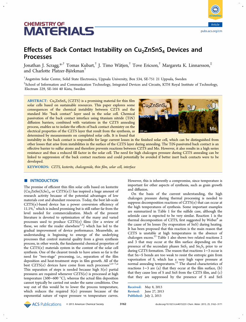
layers in samples A and B (see Table 2) have almost identicaldistributions of Cu, Zn, and Sn. There is a possibleaccumulation of Zn at the back contact in both cases (althoughthe interpretation of SIMS data at interfaces is not certainbecause of changes in sputtering rate). The right side of Figure1 shows the Na, S, and Mo profiles for the same samples. Wesee that the TiN layer had essentially no influence on the Nacontent and distribution in sample B. The only clear differencebetween the samples is that the Mo and S signals peak at theback contact interface in sample A, whereas in sample B nopeak is seen for either element. This is initial evidence for thepresence of a thicker layer of MoS2 in sample A compared withsample B.Figure 2a and Figure 2b show cross-sectional SEM images
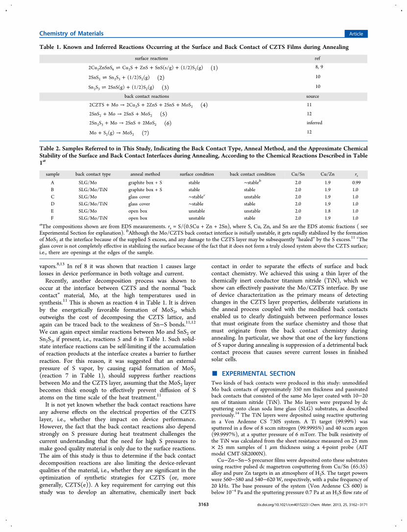
taken at the back contact region in samples A and B, those thatwere annealed with excess S. In sample A, with no TiN layer,
Chemistry of Materials Article
dx.doi.org/10.1021/cm4015223 | Chem. Mater. 2013, 25, 3162−31713164
the Mo is covered by an approximately 60−70 nm layer, whichwas confirmed as MoS2 by using Raman scattering; strongbands were seen at 407, 381, and 286 cm−1, as in Figure 2c.20
With the TiN layer (sample B), no MoS2 can be seen by SEM(the TiN layer itself cannot be resolved in this image), andRaman showed only extremely weak bands for MoS2 (Figure2d). These differences in MoS2 thickness between A and B areconsistent with the SIMS results. We conclude that even thisthin TiN layer is an effective barrier to S atoms, preventing Svapor from reacting with the underlying Mo.To determine whether the TiN also prevents reactions
between Mo and the CZTS layer itself, we examined the backcontacts of samples C and D, which were annealed without
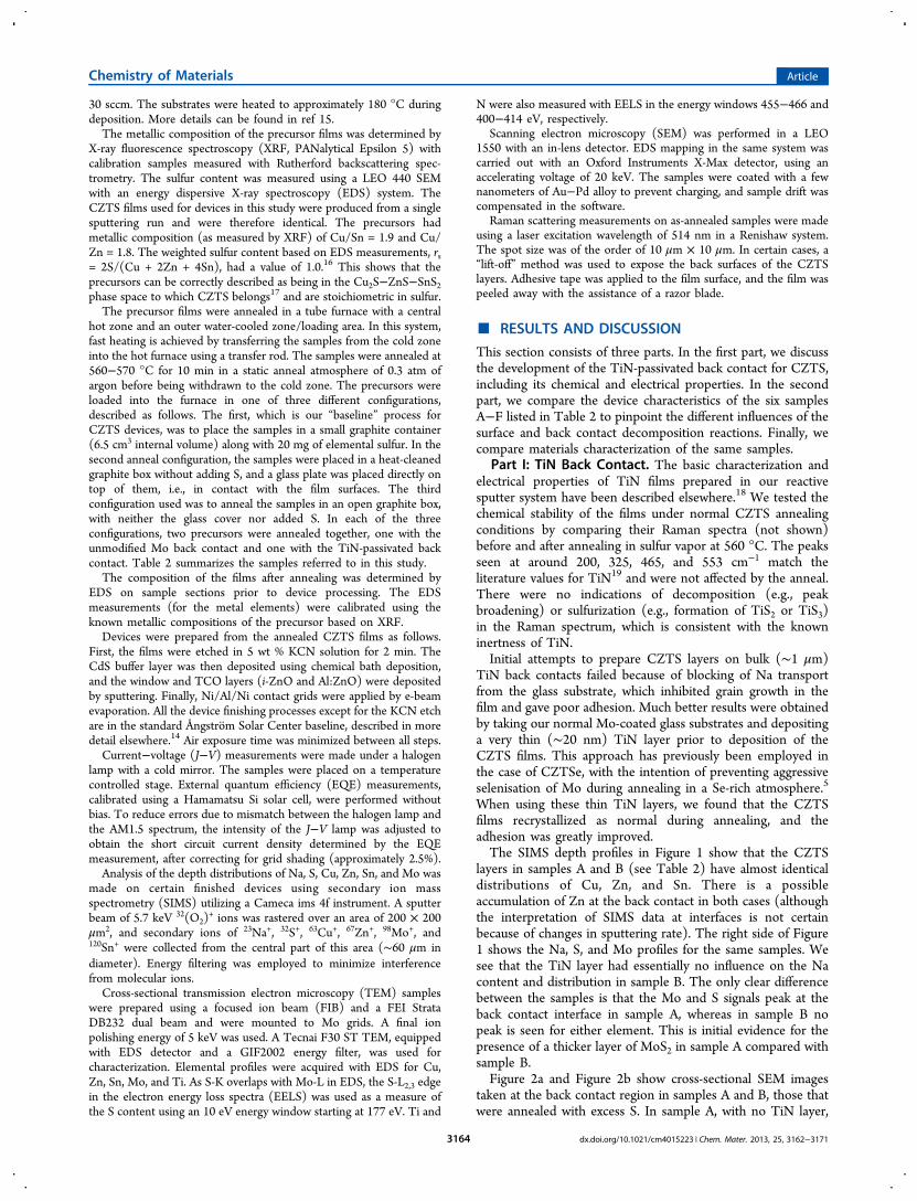
added sulfur. Figure 3a and Figure 3b show TEM cross sectionsof the back contact regions of these samples. With the
unmodified back contact (sample C), an approximately 30 nmMoS2 layer can be seen (the thinner layer reflecting the loweravailability of S in this anneal configuration). To confirm thatthis did not arise from residual S vapor in the annealing system,we annealed a bare Mo piece in the same configuration. In thatcase, no MoS2 could be resolved by SEM, and the Ramanintensity of MoS2 peaks was comparable to that in Figure 2d.Thus, the MoS2 layer seen in Figure 3a must come mainly fromthe reaction between Mo and the CZTS film. In sample D,Figure 3b, the TiN layer can just be visualized, a 10−20 nmthick, conformal coating on the Mo. Elemental depth profilesfrom EDS and EELS are shown for samples C and D in Figure3c and Figure 3d. The MoS2 in sample C is clear. In sample D,the TiN layer can be seen, and we note that the S concentrationbelow the TiN layer is negligible. In the previous work on TiNbarriers for CZTSe films, a mixed TiN/MoSe2 layer was foundafter selenization.5 In the present case, the TiN layer remainsintact, which may be because of differences in the quality (e.g.,uniformity, stoichiometry, or density) of the respective TiNlayers or because of differences in the annealing processes forthe CZTS(e) films. We can conclude that the thin TiN layersused here almost completely block sulfurization of theunderlying Mo, both from an excess S pressure in the annealingatmosphere and crucially from reaction with the CZTS layeritself.Table 3 shows the device metrics and diode parameters for
samples A−F, determined from fitting of the one-diode modelto the current voltage (J−V) data using the proceduredescribed by Hegedus and Shafarman.21 Since the J−V curvesunder illumination typically exhibited voltage-dependent carriercollection, we give here only the parameters extracted from thedark curves, which give the more reliable fit to the one-diodemodel. Sample A represents our baseline CZTS device process,having a standard Mo back contact and being annealed in Svapor excess. The device efficiency of 7.9% is among the betterreported efficiencies for pure sulfide CZTS devices at the time
Figure 1. Overlaid SIMS depth profiles for completed devices A(dotted lines) and B (solid lines). Sample B has a TiN layer at the backcontact: (left) Cu, Zn, and Sn profiles; (right) Na, S, and Mo profiles.The vertical lines at about 190 and 700 s respectively indicateestimates of the front and back interface locations of the CZTS layersand can be used to compare the left and right plots. The devicestructure is ZnO/CdS/CZTS (∼2 μm)/(TiN)/Mo/glass, with theZnO layer being to the left in the figure.
Figure 2. Above: SEM cross section images in the back contact regionsof (a) sample A (Mo back contact) and (b) sample B (TiN-coated Moback contact) after annealing. Areas where the CZTS film had flakedaway during sectioning were chosen to more clearly reveal the backcontact. Below: Raman spectra of respective back contacts of (c)sample A and (d) sample B after annealing and mechanical removal ofthe CZTS layers. The indicated peak positions correspond to MoS2.
Figure 3. Bright field TEM images of back contacts in (a) sample C,showing MoS2 layer, and (b) sample D, showing TiN layer. Below:elemental profiles in the back contact regions of (c) sample C and (d)sample D, from EDS (Cu, Zn, Sn, Mo, Ti) and EELS (S, N, Ti)measurements on TEM cross sections.
Chemistry of Materials Article
dx.doi.org/10.1021/cm4015223 | Chem. Mater. 2013, 25, 3162−31713165
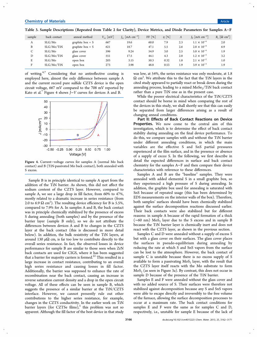
of writing.4,7 Considering that no antireflective coating isemployed here, almost the only difference between sample Aand the current record pure sulfide CZTS device is the opencircuit voltage, 667 mV compared to the 708 mV reported byKato et al.7 Figure 4 shows J−V curves for devices A and B.
Sample B is in principle identical to sample A apart from theaddition of the TiN barrier. As shown, this did not affect thesodium content of the CZTS layer. However, compared tosample A, we see a large drop in fill factor, from 60% to 47%,mostly related to a dramatic increase in series resistance (from2.0 to 6.9 Ω cm2). The resulting device efficiency for B is 5.5%,compared to 7.9% for A. In samples A and B, the back contactwas in principle chemically stabilized by the presence of excessS during annealing (both samples) and by the presence of thebarrier layer (sample B only), so we do not attribute thedifferences between devices A and B to changes in the CZTSlayer at the back contact (this is discussed in more detailbelow). In addition, the bulk resistivity of the TiN layers, ataround 130 μΩ cm, is far too low to contribute directly to theoverall series resistance. In fact, the observed losses in deviceperformance for sample B are similar to those seen when ZrNback contacts are used for CIGS, where it has been suggestedthat a barrier for majority carriers is formed.22 This resulted in alarge increase in contact resistance, contributing to an overallhigh series resistance and causing losses in fill factor.Additionally, the barrier was supposed to enhance the rate ofrecombination near the back contact, causing an increase inreverse saturation current density and a drop in the open circuitvoltage. All of these effects can be seen in sample B, whichsuggests the presence of a similar barrier at the TiN/CZTSinterface. However, we cannot presently rule out othercontributions to the higher series resistance, for example,changes in the CZTS conductivity. In the earlier work on TiNbarrier layers (for CZTSe films),5 this problem was not soapparent. Although the fill factor of the best device in that study
was low, at 54%, the series resistance was only moderate, at 1.8Ω cm2. We attribute this to the fact that the TiN layers in thecited study appeared to partially react or break down during theannealing process, leading to a mixed MoSe2/TiN back contactrather than a pure TiN one as in the present case.While the poorer electrical characteristics of the TiN/CZTS
contact should be borne in mind when comparing the rest ofthe devices in this study, we shall shortly see that this can easilybe separated from larger differences arising as a result ofchanging anneal conditions.
Part II: Effects of Back Contact Reactions on DeviceProperties. We now come to the central aim of thisinvestigation, which is to determine the effect of back contactstability during annealing on the final device performance. Todo this, we compare samples with and without the TiN barrierunder different annealing conditions, in which the mainvariables are the effective S and SnS partial pressuresexperienced at the film surface, and in the presence or absenceof a supply of excess S. In the following, we first describe indetail the expected differences in surface and back contactchemistry for the samples A−F and then compare their devicecharacteristics with reference to these differences.Samples A and B are the “baseline” samples. They were
annealed with added elemental S in a small graphite box, sothey experienced a high pressure of S during annealing. Inaddition, the graphite box used for annealing is saturated withSnS because of repeated usage (this has been determined byEDS measurements on the interior walls of the box). Therefore,both samples’ surfaces should have been chemically stabilizedagainst the surface decomposition reactions discussed earlier.Their back contacts were also stabilized but for differentreasons: in sample A because of the rapid formation of a thick(∼60 nm) MoS2 layer due to the S excess and in sample Bbecause the TiN barrier layer is chemically inert and does notreact with the CZTS layer, as shown in the previous section.Samples C and D were annealed without a supply of excess S
but with a glass cover on their surfaces. The glass cover placesthe surfaces in pseudo-equilibrium during annealing byreducing the rate at which S and SnS vapors from the surfacecan be lost to the atmosphere. However, the back contact ofsample C is unstable because there is no excess supply of Savailable to form a passivating MoS2 layer, with the result thatthe CZTS layer itself reacts with the Mo substrate to formMoS2 (as seen in Figure 3a). By contrast, this does not occur insample D because of the presence of the TiN barrier.Samples E and F were annealed without the glass cover and
with no added source of S. Their surfaces were therefore notstabilized against decomposition because any S and SnS vaporswere able to escape directly and irreversibly to the free volumeof the furnace, allowing the surface decomposition processes tooccur at a maximum rate. The back contact conditions forsamples E and F were the same as for samples C and D,respectively, i.e., unstable for sample E because of the lack of
Table 3. Sample Descriptions (Repeated from Table 2 for Clarity), Device Metrics, and Diode Parameters for Samples A−F
sample back contact anneal method Voc [mV] Jsc [mA cm−2] FF [%] η [%] A J0 [mA cm−2] Rs [Ω cm2]
A SLG/Mo graphite box + S 667 19.6 60.0 7.9 2.3 1.1 × 10⁻⁴ 2.0B SLG/Mo/TiN graphite box + S 621 18.7 47.1 5.5 2.6 2.8 × 10⁻⁴ 6.9C SLG/Mo glass cover 596 9.24 54.9 3.0 2.5 5.8 × 10⁻⁴ 1.9D SLG/Mo/TiN glass cover 551 17.5 44.1 4.3 2.8 1.2 × 10⁻³ 3.2E SLG/Mo open box 203 3.15 50.3 0.32 1.8 2.1 × 10⁻² 1.0F SLG/Mo/TiN open box 273 3.98 48.8 0.53 1.9 3.9 × 10⁻³ 1.9
Figure 4. Current−voltage curves for samples A (normal Mo backcontact) and B (TiN-passivated Mo back contact), both annealed withS excess.
Chemistry of Materials Article
dx.doi.org/10.1021/cm4015223 | Chem. Mater. 2013, 25, 3162−31713166
external S supply (MoS2 forming by reaction with the CZTSlayer) and stable for sample F because of the TiN barrier layer.Table 2 summarizes the above discussion by indicating whetherthe surfaces and back contacts were stable or not during CZTSsynthesis. The sample compositions after annealing are alsoshown. Table 3 shows device and diode parameters. Weemphasize that since all other process steps were identical, thedifferences in device performance for samples with the sametype of back contact can only be due to changes in the CZTSlayers as a result of the described chemical differences duringannealing.External quantum efficiency (EQE) and J−V curves for the
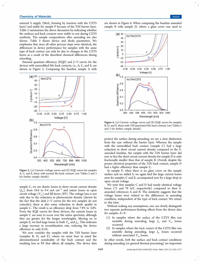
devices with unmodified Mo back contacts, i.e., A, C, and E, areshown in Figure 5. Comparing the baseline sample A with
sample C, we see drastic losses in short circuit current density(Jsc), from 19.6 to 9.4 mA cm−2 and minor losses in opencircuit voltage (Voc) and fill factor (FF). The voltage loss is notonly due to the reduction in photocurrent density (shown bythe fact that the dark J−V curves for the two samples do notcoincide); there is also some reduction in diode quality insample C. The result is an efficiency drop from 7.9% to 3.0%.From the EQE curves for these devices, the current losses insample C are seen to occur over the entire spectrum, althoughthey are greater for the longer wavelengths. Moving on tosample E, we find large losses in both Voc and Jsc. This indicatesa large increase in recombination rate, reducing the deviceefficiency to only 0.3%.We now consider the samples with the TiN barrier layer
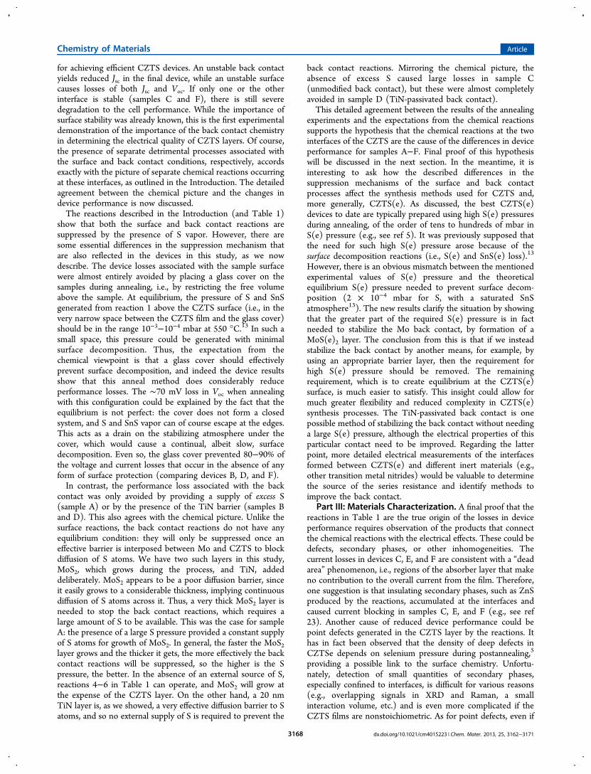
(samples B, D, and F), where we must bear in mind theaforementioned nonideality of the back contact and theresulting loss in FF that affects all samples. The device data
are shown in Figure 6. When comparing the baseline annealedsample B with sample D, where a glass cover was used to
protect the surface during annealing, we see a clear distinctionfrom the case without the barrier layer. Whereas the samplewith the unmodified back contact (sample C) had a largereduction in short circuit current density compared to the S-annealed baseline, the sample with the TiN barrier layer didnot; in fact the short circuit current density for sample D is onlyfractionally smaller than that of sample B. Overall, despite thepoorer electrical properties of the TiN back contact, sample Dhad a higher efficiency than sample C.In sample F, when there is no glass cover on the sample
surface and no added S, we again find the large current lossesseen for samples C and E, accompanied now by a large drop inopen circuit voltage.We note that samples C and D had nearly identical voltage
losses (71 and 70 mV, respectively) compared to their S-annealed references A and B. The similarity suggests that thevoltage losses were related to the differences in annealingcondition, independent of the type of back contact. We returnto this later.Without making any assumptions, one can clearly distinguish
two separate performance-limiting effects from the device datafor samples A−F:(1) In samples where the surface of the CZTS film was
unstable during annealing, large Jsc and Voc lossesoccurred.
(2) In samples where the back contact of the CZTS film wasunstable during annealing, large Jsc losses occurredwithout associated Voc losses.
In other words, both the surface and back contact conditionsduring annealing (or general thermal processing) are important
Figure 5. (a) Current−voltage curves and (b) EQE curves for samplesA, C, and E, those with normal Mo back contacts (see Tables 2 and 3for further sample details).
Figure 6. (a) Current−voltage curves and (b) EQE curves for samplesB, D, and F, those with TiN-passivated Mo back contacts (see Tables 2and 3 for further sample details).
Chemistry of Materials Article
dx.doi.org/10.1021/cm4015223 | Chem. Mater. 2013, 25, 3162−31713167
for achieving efficient CZTS devices. An unstable back contactyields reduced Jsc in the final device, while an unstable surfacecauses losses of both Jsc and Voc. If only one or the otherinterface is stable (samples C and F), there is still severedegradation to the cell performance. While the importance ofsurface stability was already known, this is the first experimentaldemonstration of the importance of the back contact chemistryin determining the electrical quality of CZTS layers. Of course,the presence of separate detrimental processes associated withthe surface and back contact conditions, respectively, accordsexactly with the picture of separate chemical reactions occurringat these interfaces, as outlined in the Introduction. The detailedagreement between the chemical picture and the changes indevice performance is now discussed.The reactions described in the Introduction (and Table 1)
show that both the surface and back contact reactions aresuppressed by the presence of S vapor. However, there aresome essential differences in the suppression mechanism thatare also reflected in the devices in this study, as we nowdescribe. The device losses associated with the sample surfacewere almost entirely avoided by placing a glass cover on thesamples during annealing, i.e., by restricting the free volumeabove the sample. At equilibrium, the pressure of S and SnSgenerated from reaction 1 above the CZTS surface (i.e., in thevery narrow space between the CZTS film and the glass cover)should be in the range 10−3−10−4 mbar at 550 °C.13 In such asmall space, this pressure could be generated with minimalsurface decomposition. Thus, the expectation from thechemical viewpoint is that a glass cover should effectivelyprevent surface decomposition, and indeed the device resultsshow that this anneal method does considerably reduceperformance losses. The ∼70 mV loss in Voc when annealingwith this configuration could be explained by the fact that theequilibrium is not perfect: the cover does not form a closedsystem, and S and SnS vapor can of course escape at the edges.This acts as a drain on the stabilizing atmosphere under thecover, which would cause a continual, albeit slow, surfacedecomposition. Even so, the glass cover prevented 80−90% ofthe voltage and current losses that occur in the absence of anyform of surface protection (comparing devices B, D, and F).In contrast, the performance loss associated with the back
contact was only avoided by providing a supply of excess S(sample A) or by the presence of the TiN barrier (samples Band D). This also agrees with the chemical picture. Unlike thesurface reactions, the back contact reactions do not have anyequilibrium condition: they will only be suppressed once aneffective barrier is interposed between Mo and CZTS to blockdiffusion of S atoms. We have two such layers in this study,MoS2, which grows during the process, and TiN, addeddeliberately. MoS2 appears to be a poor diffusion barrier, sinceit easily grows to a considerable thickness, implying continuousdiffusion of S atoms across it. Thus, a very thick MoS2 layer isneeded to stop the back contact reactions, which requires alarge amount of S to be available. This was the case for sampleA: the presence of a large S pressure provided a constant supplyof S atoms for growth of MoS2. In general, the faster the MoS2layer grows and the thicker it gets, the more effectively the backcontact reactions will be suppressed, so the higher is the Spressure, the better. In the absence of an external source of S,reactions 4−6 in Table 1 can operate, and MoS2 will grow atthe expense of the CZTS layer. On the other hand, a 20 nmTiN layer is, as we showed, a very effective diffusion barrier to Satoms, and so no external supply of S is required to prevent the
back contact reactions. Mirroring the chemical picture, theabsence of excess S caused large losses in sample C(unmodified back contact), but these were almost completelyavoided in sample D (TiN-passivated back contact).This detailed agreement between the results of the annealing
experiments and the expectations from the chemical reactionssupports the hypothesis that the chemical reactions at the twointerfaces of the CZTS are the cause of the differences in deviceperformance for samples A−F. Final proof of this hypothesiswill be discussed in the next section. In the meantime, it isinteresting to ask how the described differences in thesuppression mechanisms of the surface and back contactprocesses affect the synthesis methods used for CZTS and,more generally, CZTS(e). As discussed, the best CZTS(e)devices to date are typically prepared using high S(e) pressuresduring annealing, of the order of tens to hundreds of mbar inS(e) pressure (e.g., see ref 5). It was previously supposed thatthe need for such high S(e) pressure arose because of thesurface decomposition reactions (i.e., S(e) and SnS(e) loss).13
However, there is an obvious mismatch between the mentionedexperimental values of S(e) pressure and the theoreticalequilibrium S(e) pressure needed to prevent surface decom-position (2 × 10⁻⁴ mbar for S, with a saturated SnSatmosphere13). The new results clarify the situation by showingthat the greater part of the required S(e) pressure is in factneeded to stabilize the Mo back contact, by formation of aMoS(e)2 layer. The conclusion from this is that if we insteadstabilize the back contact by another means, for example, byusing an appropriate barrier layer, then the requirement forhigh S(e) pressure should be removed. The remainingrequirement, which is to create equilibrium at the CZTS(e)surface, is much easier to satisfy. This insight could allow formuch greater flexibility and reduced complexity in CZTS(e)synthesis processes. The TiN-passivated back contact is onepossible method of stabilizing the back contact without needinga large S(e) pressure, although the electrical properties of thisparticular contact need to be improved. Regarding the latterpoint, more detailed electrical measurements of the interfacesformed between CZTS(e) and different inert materials (e.g.,other transition metal nitrides) would be valuable to determinethe source of the series resistance and identify methods toimprove the back contact.
Part III: Materials Characterization. A final proof that thereactions in Table 1 are the true origin of the losses in deviceperformance requires observation of the products that connectthe chemical reactions with the electrical effects. These could bedefects, secondary phases, or other inhomogeneities. Thecurrent losses in devices C, E, and F are consistent with a “deadarea” phenomenon, i.e., regions of the absorber layer that makeno contribution to the overall current from the film. Therefore,one suggestion is that insulating secondary phases, such as ZnSproduced by the reactions, accumulated at the interfaces andcaused current blocking in samples C, E, and F (e.g., see ref23). Another cause of reduced device performance could bepoint defects generated in the CZTS layer by the reactions. Ithas in fact been observed that the density of deep defects inCZTSe depends on selenium pressure during postannealing,5
providing a possible link to the surface chemistry. Unfortu-nately, detection of small quantities of secondary phases,especially confined to interfaces, is difficult for various reasons(e.g., overlapping signals in XRD and Raman, a smallinteraction volume, etc.) and is even more complicated if theCZTS films are nonstoichiometric. As for point defects, even if
Chemistry of Materials Article
dx.doi.org/10.1021/cm4015223 | Chem. Mater. 2013, 25, 3162−31713168
defect energy levels can be detected, assigning them to aparticular defect type and determining the origin of this defectare extremely difficult. Accordingly, while we find someinteresting differences between samples A−F in the materialscharacterization, we cannot conclusively determine the reasonsfor device performance differences. We include the main resultshere for the sake of completeness.First, considering the EDS compositions of samples A−F
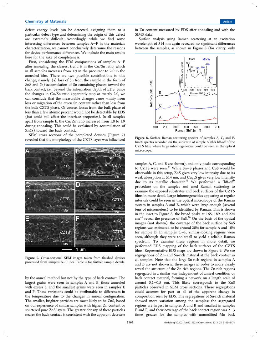
after annealing, the clearest trend is in the Cu/Sn ratio, whichin all samples increases from 1.9 in the precursor to 2.0 in theannealed film. There are two possible contributions to thischange, namely, (a) loss of Sn from the sample in the form ofSnS and (b) accumulation of Sn-containing phases toward theback contact, i.e., beyond the information depth of EDS. Sincethe changes in Cu/Sn ratio apparently stop at exactly 2.0, wecan conclude that the measurable changes came mainly fromloss or migration of the excess Sn content rather than loss fromthe bulk CZTS phase. Of course, losses from the bulk phase ofless than a few atomic percent would not be detectable by EDS(but could still affect the interface properties). In all samplesapart from sample E, the Cu/Zn ratio increased from 1.8 to 1.9during annealing. This could be explained by accumulation ofZn(S) toward the back contact.SEM cross sections of the completed devices (Figure 7)
revealed that the morphology of the CZTS layer was influenced
by the anneal method but not by the type of back contact. Thelargest grains were seen in samples A and B, those annealedwith excess S, and the smallest grains were seen in samples Eand F. These variations could be attributable to differences inthe temperature due to the changes in anneal configuration.The smaller, brighter particles are most likely to be ZnS, basedon our experience of similar samples with higher Zn content orsputtered pure ZnS layers. The greater density of these particlesnearer the back contact is consistent with the apparent decrease
in Zn content measured by EDS after annealing and with theSIMS data.Surface analysis using Raman scattering at an excitation
wavelength of 514 nm again revealed no significant differencesbetween the samples, as shown in Figure 8 (for clarity, only
samples A, C, and E are shown), and only peaks correspondingto CZTS were seen.24 While Sn−S phases and CuS would beobservable in this setup, ZnS gives very low intensity due to itsweak absorption at 514 nm, and Cu2‑xS gives very low intensitydue to its metallic character.25 We performed a “lift-off”procedure on the samples and used Raman scattering toexamine the exposed substrates and back surfaces of the CZTSfilms in more detail. Large inhomogeneities appearing at regularintervals could be seen in the optical microscope of the Ramansystem in samples A and B, which were large enough (severaltens of micrometers) to be identified by Raman. This is shownin the inset to Figure 8; the broad peaks at 165, 189, and 224cm−1 reveal the presence of SnS.26 On the basis of the opticalimages (not shown), the coverage of the back surface by SnSregions was estimated to be around 20% for sample A and 10%for sample B. In samples C−F, similar-looking regions wereseen, although they were too small to yield a reliable Ramanspectrum. To examine these regions in more detail, weperformed EDS mapping of the back surfaces of the CZTSfilms. Representative EDS maps are shown in Figure 9. We seesegregations of Zn- and Sn-rich material at the back contact inall samples. Note that the large Sn-rich regions in samples Aand B are not shown in these images in order to more clearlyreveal the structure of the Zn-rich regions. The Zn-rich regionssegregated in a similar way independent of anneal condition orback contact material, forming a network on a length scale ofaround 0.2−0.5 μm. This likely corresponds to the ZnSparticles observed in SEM cross sections. These segregationscould account for part or all of the apparent change incomposition seen by EDS. The segregations of Sn-rich materialshowed more variation among the samples: the segregatedregions are largest in samples A and B and smallest in samplesE and F, and their coverage of the back contact region was 2−3times greater for the samples with unmodified Mo back
Figure 7. Cross-sectional SEM images taken from finished devicesprocessed from samples A−F. See Table 2 for further sample details.
Figure 8. Surface Raman scattering spectra of samples A, C, and E.Inset: spectra recorded on the substrate of sample A after lift-off of theCZTS film, where large inhomogeneities could be seen in the opticalmicroscope.
Chemistry of Materials Article
dx.doi.org/10.1021/cm4015223 | Chem. Mater. 2013, 25, 3162−31713169
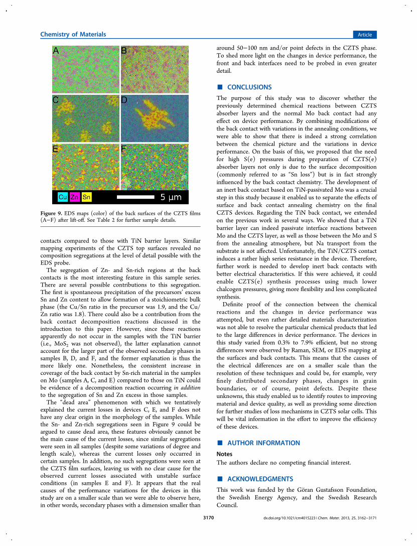
contacts compared to those with TiN barrier layers. Similarmapping experiments of the CZTS top surfaces revealed nocomposition segregations at the level of detail possible with theEDS probe.The segregation of Zn- and Sn-rich regions at the back
contacts is the most interesting feature in this sample series.There are several possible contributions to this segregation.The first is spontaneous precipitation of the precursors’ excessSn and Zn content to allow formation of a stoichiometric bulkphase (the Cu/Sn ratio in the precursor was 1.9, and the Cu/Zn ratio was 1.8). There could also be a contribution from theback contact decomposition reactions discussed in theintroduction to this paper. However, since these reactionsapparently do not occur in the samples with the TiN barrier(i.e., MoS2 was not observed), the latter explanation cannotaccount for the larger part of the observed secondary phases insamples B, D, and F, and the former explanation is thus themore likely one. Nonetheless, the consistent increase incoverage of the back contact by Sn-rich material in the sampleson Mo (samples A, C, and E) compared to those on TiN couldbe evidence of a decomposition reaction occurring in additionto the segregation of Sn and Zn excess in those samples.The “dead area” phenomenon with which we tentatively
explained the current losses in devices C, E, and F does nothave any clear origin in the morphology of the samples. Whilethe Sn- and Zn-rich segregations seen in Figure 9 could beargued to cause dead area, these features obviously cannot bethe main cause of the current losses, since similar segregationswere seen in all samples (despite some variations of degree andlength scale), whereas the current losses only occurred incertain samples. In addition, no such segregations were seen atthe CZTS film surfaces, leaving us with no clear cause for theobserved current losses associated with unstable surfaceconditions (in samples E and F). It appears that the realcauses of the performance variations for the devices in thisstudy are on a smaller scale than we were able to observe here,in other words, secondary phases with a dimension smaller than
around 50−100 nm and/or point defects in the CZTS phase.To shed more light on the changes in device performance, thefront and back interfaces need to be probed in even greaterdetail.
■ CONCLUSIONS
The purpose of this study was to discover whether thepreviously determined chemical reactions between CZTSabsorber layers and the normal Mo back contact had anyeffect on device performance. By combining modifications ofthe back contact with variations in the annealing conditions, wewere able to show that there is indeed a strong correlationbetween the chemical picture and the variations in deviceperformance. On the basis of this, we proposed that the needfor high S(e) pressures during preparation of CZTS(e)absorber layers not only is due to the surface decomposition(commonly referred to as “Sn loss”) but is in fact stronglyinfluenced by the back contact chemistry. The development ofan inert back contact based on TiN-passivated Mo was a crucialstep in this study because it enabled us to separate the effects ofsurface and back contact annealing chemistry on the finalCZTS devices. Regarding the TiN back contact, we extendedon the previous work in several ways. We showed that a TiNbarrier layer can indeed passivate interface reactions betweenMo and the CZTS layer, as well as those between the Mo and Sfrom the annealing atmosphere, but Na transport from thesubstrate is not affected. Unfortunately, the TiN/CZTS contactinduces a rather high series resistance in the device. Therefore,further work is needed to develop inert back contacts withbetter electrical characteristics. If this were achieved, it couldenable CZTS(e) synthesis processes using much lowerchalcogen pressures, giving more flexibility and less complicatedsynthesis.Definite proof of the connection between the chemical
reactions and the changes in device performance wasattempted, but even rather detailed materials characterizationwas not able to resolve the particular chemical products that ledto the large differences in device performance. The devices inthis study varied from 0.3% to 7.9% efficient, but no strongdifferences were observed by Raman, SEM, or EDS mapping atthe surfaces and back contacts. This means that the causes ofthe electrical differences are on a smaller scale than theresolution of these techniques and could be, for example, veryfinely distributed secondary phases, changes in grainboundaries, or of course, point defects. Despite theseunknowns, this study enabled us to identify routes to improvingmaterial and device quality, as well as providing some directionfor further studies of loss mechanisms in CZTS solar cells. Thiswill be vital information in the effort to improve the efficiencyof these devices.
■ AUTHOR INFORMATION
NotesThe authors declare no competing financial interest.
■ ACKNOWLEDGMENTS
This work was funded by the Goran Gustafsson Foundation,the Swedish Energy Agency, and the Swedish ResearchCouncil.
Figure 9. EDS maps (color) of the back surfaces of the CZTS films(A−F) after lift-off. See Table 2 for further sample details.
Chemistry of Materials Article
dx.doi.org/10.1021/cm4015223 | Chem. Mater. 2013, 25, 3162−31713170
■ ADDITIONAL NOTEaWe also consider the coevaporation process employed in ref 6as a two-stage process, since an in situ anneal in Sn and Sevapor is performed as a critical step after the main part of filmdeposition.
■ REFERENCES(1) Todorov, T. K.; Tang, J.; Bag, S.; Gunawan, O.; Gokmen, T.;Zhu, Y.; Mitzi, D. B. Adv. Energy Mater. 2013, 3, 34.(2) Mitzi, D. B.; Gunawan, O.; Todorov, T. K.; Wang, K.; Guha, S.Sol. Energy Mater. Sol. Cells 2011, 95.(3) Wang, H. Int. J. Photoenergy 2011, 801292, DOI: 10.1155/2011/801292.(4) Shin, B.; Gunawan, O.; Zhu, Y.; Bojarczuk, N. A.; Chey, S. J.;Guha, S. Prog. Photovolt. Res. Appl. 2013, 21, 72.(5) Shin, B.; Zhu, Y.; Bojarczuk, N. A.; Chey, S. J.; Guha, S. Appl.Phys. Lett. 2012, 101, 053903.(6) Repins, I.; Beall, C.; Vora, N.; DeHart, C.; Kuciauskas, D.; Dippo,P.; To, B.; Mann, J.; Hsu, W.-C.; Goodrich, A.; Noufi, R. Sol. EnergyMater. Sol. Cells 2012, 101, 154.(7) Kato, T.; Hiroi, H.; Sakai, N.; Muraoka, S.; Sugimoto, H.Proceedings of the 27th European Photovoltaic Solar Energy Conferenceand Exhibition, Frankfurt, Germany, 2012; EU PVSEC, 2012; p 2236.(8) Redinger, A.; Berg, D. M.; Dale, P. J.; Siebentritt, S. J. Am. Chem.Soc. 2011, 133, 3320.(9) Weber, A.; Mainz, R.; Schock, H. W. J. Appl. Phys. 2010, 107.(10) Piacente, V.; Foglia, S.; Scardala, P. J. Alloys Compd. 1991, 177,17.(11) Scragg, J. J.; Watjen, J. T.; Edoff, M.; Ericson, T.; Kubart, T.;Platzer-Bjorkman, C. J. Am. Chem. Soc. 2012, 134, 19330.(12) Scragg, J. J.; Dale, P. J.; Colombara, D.; Peter, L. M.ChemPhysChem 2012, 13, 3035.(13) Scragg, J. J.; Ericson, T.; Kubart, T.; Edoff, M.; Platzer-Bjorkman, C. Chem. Mater. 2011, 23, 4625.(14) Lindahl, J.; Zimmermann, U.; Szaniawski, P.; Torndahl, T.;Hultqvist, A.; Salome, P.; Platzer-Bjorkman, C.; Edoff, M. IEEE J.Photovoltaics 2013, 1.(15) Ericson, T.; Kubart, T.; Scragg, J. J.; Platzer-Bjorkman, C. ThinSolid Films 2012, 520, 7093.(16) Scragg, J. J.; Ericson, T.; Fontane, X.; Izquierdo-Roca, V.; Perez-Rodríguez, A.; Kubart, T.; Edoff, M.; Platzer-Bjorkman, C. Prog.Photovoltaics: Res. Appl. [Online early access]. DOI: 10.1002/pip.2265.Published Online: July 10, 2012.(17) Olekseyuk, I. D.; Dudchak, I. V.; Piskach, L. V. J. Alloys Compd.2004, 368, 135.(18) Westlinder, J.; Sjoblom, G.; Olsson, J. Microelectron. Eng. 2004,75 (4), 389−396.(19) Constable, C. P.; Yarwood, J.; Munz, W.-D. Surf. Coat. Technol.1999, 116−119, 155−159.(20) Sandoval, S. J.; Yang, D.; Frindt, R. F.; Irwin, J. C. Phys. Rev. B1991, 44, 3955.(21) Hegedus, S. S.; Shafarman, W. N. Prog. Photovoltaics: Res. Appl.2004, 12, 155.(22) Malmstrom, J.; Schleussner, S.; Stolt, L. Appl. Phys. Lett. 2004,85, 2634.(23) Watjen, J. T.; Engman, J.; Edoff, M.; Platzer-Bjorkman, C. Appl.Phys. Lett. 2012, 100, 173510.(24) Fontane, X.; Calvo-Barrio, L.; Izquierdo-Roca, V.; Saucedo, E.;Perez-Rodriguez, A.; Morante, J. R.; Berg, D. M.; Dale, P. J.;Siebentritt, S. Appl. Phys. Lett. 2011, 98, 181905.(25) Munce, C. G.; Parker, G. K.; Holt, S. A.; Hope, G. A. ColloidsSurf., A 2007, 295, 152.(26) Parkin, I. P.; Price, L. S.; Hibbert, T. G.; Molloy, K. C. J. Mater.Chem. 2001, 11, 1486.
Chemistry of Materials Article
dx.doi.org/10.1021/cm4015223 | Chem. Mater. 2013, 25, 3162−31713171