Embed Size (px)
Citation preview

EECS 473Advanced Embedded Systems
Lecture 11ish:
Power review & Switching power supplies
A number of slides taken from UT-Austin’s EE462L power electronics class.http://users.ece.utexas.edu/~kwasinski/EE462LS14.html -- very useful!

Random stuffs
• Project– Has everyone signed up for the Expo?
• Ford is the sponsor
• Office hours shift tomorrow (and break)– Friday 9-10:30am (instead of 10:30-12)– Will hold hours on Tuesday from 3-4:30
• different time than normal, usually 470 only this is 473 only
– Today’s office hours are going to get slammed by 470 students (they have an exam today)
• HW1 is due on Wednesday @10pm

Group status
• No team status today
– Will pick up after break.

What are DC converters?
• DC converters convert one DC voltage level to another.
– Very commonly on PCBs• Often have USB or battery power
• But might need 1.8V, 3.3V, 5V, 12V and -12V all on the same board.
– On-PCB converters allow us to do that
Images from http://itpedia.nyu.edu/wiki/File:V_reg_7805.jpg, http://www.electronics-lab.com/blog/wp-content/uploads/2007/10/p1000255.JPG
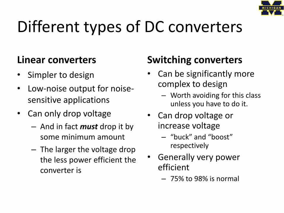
Different types of DC converters
Linear converters Switching converters
• Simpler to design
• Low-noise output for noise-sensitive applications
• Can only drop voltage
– And in fact must drop it by some minimum amount
– The larger the voltage drop the less power efficient the converter is
• Can be significantly more complex to design– Worth avoiding for this class
unless you have to do it.
• Can drop voltage or increase voltage– “buck” and “boost”
respectively
• Generally very power efficient– 75% to 98% is normal

Characteristics of DC Converters• To better understand how to pick a converter we will go over the
following characteristics seen in all DC converters
– Power wasted (as heat)
– Quiescent current, 𝐼𝑄• The leakage current that occurs regardless of operation.
– Power supply rejection ratio (PSRR)• The ability to reject output noise at different frequency
– External capacitors and equivalent series resistance(ESR)
• Output noise filter that helps keeping the signal clean
• These characteristics are what people generally look for when selecting converters, but they’re not by any means the only characteristics that matter.

1. Power Wasted (as Heat)• Linear converters waste power = (Vin– Vout)*Iload
– Example• 12 V battery supplying 5V to each device
– Microcontroller that draws 5mA – Ultrasonic rangefinder that draws 50mA
• Use LM7805 (linear regulator) to drop 12V to 5V• Power wasted = (12V – 5V) * (0.050A + 0.005A) = 0.385W
– Which is actually more than the power consumed!– Is this acceptable?
» Hope so, because the alternative (switching converter) is a lot more difficult.
• Switchers generally waste a more-or-less fixed percent– Say 15% or so, but as little as 3% is reasonable.
http://www.dimensionengineering.com/info/switching-regulators is the source for this example. They go into more detail on their site.

• In general… – All have quiescent current
(𝐼𝑄), which is different in each IC
• 𝐼𝑄 is affected by the input and temperature the device is operating at.
• Will drain battery so choose carefully when picking converters!
• For this device, IQ is huge.– Designed to move 1A.
LM7805 𝑰𝑸 during operation
2. Quiescent current, 𝐼𝑄
Diagrams from http://www.fairchildsemi.com/ds/LM/LM7805.pdf

3. Caps and ESR.
• Noise
– Capacitors!• Each converter requires at least a 𝐶𝑜𝑢𝑡 and sometimes a 𝐶𝑖𝑛 to
reduce noise in the system
– Will be specified in datasheets
– Capacitors size generally needed from smallest to largest:
» General linear converters -> LDOs -> switching converters
min 22𝝁𝑭 min 22𝝁𝑭
LDO LM2940Linear LM7805Diagrams from http://www.fairchildsemi.com/ds/LM/LM7805.pdf and http://www.ti.com/lit/ds/symlink/lm2940-n.pdf

• Capacitors aren’t the only thing that will determine stability– Sometime an operation demands higher
𝐼𝑜 and leaves the safe-operating-area (SOA) causing instability as well
• So in addition to the capacitors, equivalent series resistance (ESR) comes into play
• Like everything else, the capacitorand its ESR will be specified in
each IC’s datasheet
• There’s also more than just ESR that affects the stability as well forvaried 𝐼𝑜 and is discussed more inthe link below
http://www.bcae1.com/switchingpowersupplydesign/datasheets/ldoregulatorstabilityinfoslva115.pdf
3. Caps and ESR.

3. Caps and ESR
• So let’s take a look at an example of stability/instability with a changing 𝐼𝑜
– Note the amount of noise in the top waveform (𝑉𝑜) as 𝐼𝑜changes with the presence of ESR
Load transient with 𝟐. 𝟐𝝁𝑭 ceramic capacitor and 𝟏𝛀 ESRLoad transient with 𝟐. 𝟐𝝁𝑭 ceramic capacitor

4. Input Noise• PSRR indicates how well the supply deals
with input noise.– Recall we rely on the VRM (voltage
regulation module) to keep noise down atlow frequencies.
– We don’t want noise on the output– You can determine how well a
linear converter handle noiseby its PSRR
• PSRR is used to describe the amount of noise rejectedby a particular device
– What does PSRR mean for noise rejection?
• Take 40dB @100kHz and 1V input, so 1𝑉 ∗ 10−40
20 = .01 = 10𝑚𝑉• Meaning for every 1V there may be 10𝑚𝑉 superimposed on the output
• 70dB @ 10KHz is 1𝑉 ∗ 10−70
20 ~ .00032 = 0.32 𝑚𝑉, so 3% of the noise at 100KHz!
– PSSR performance is crucial for noise sensitive operation if you’ve got a noisy source
• Commonly switching supply followed by an LDO.
Typical PSRR profile for an LDO, 40dB @ 100kHz
Graph from digikey http://www.digikey.com/us/en/techzone/power/resources/articles/hybrid-power-supplies-noise-free-voltages.html

Quick look at the options
• Linear converter
– LDO
• Switching converter
– Buck
– Boost
– Buck-Boost

Linear converter
• One can think of a linear converter as a “smart” voltage divider.– If we were using a very small
amount of current, that would work.
– But hugely wasteful.
• Instead, we want the topresistor to vary with the load.– As load draws more current,
R1 drops resistance to keepvoltage constant.
Figures on this slide and the next taken from http://cds.linear.com/docs/en/application-note/AN140fa.pdf, which is a great app-note.

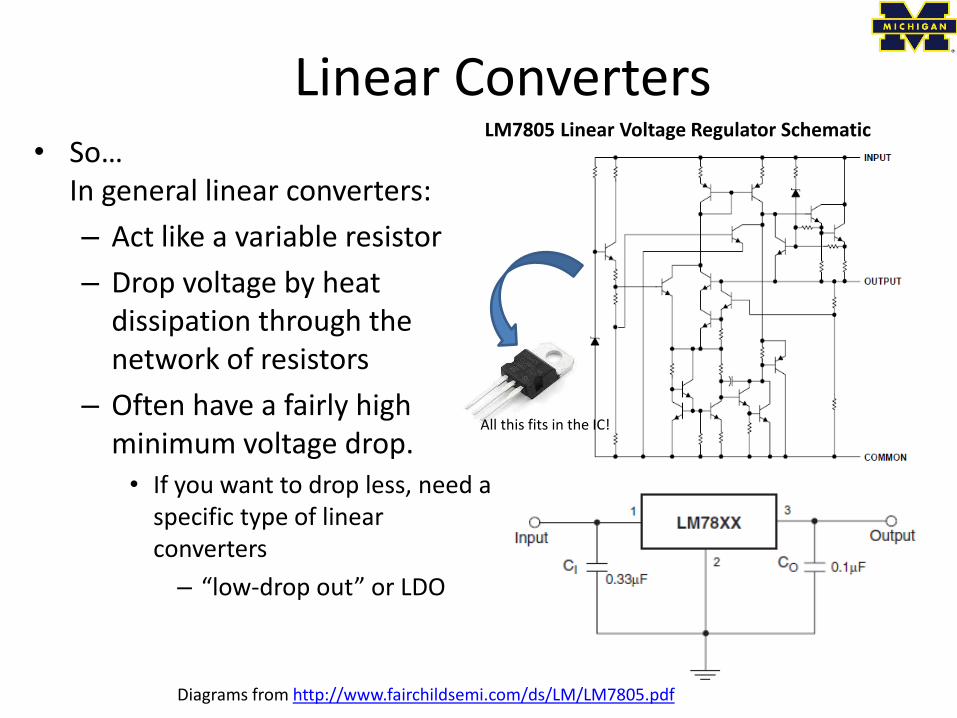
Linear Converters• So…
In general linear converters:
– Act like a variable resistor
– Drop voltage by heat dissipation through the network of resistors
– Often have a fairly high minimum voltage drop.
• If you want to drop less, need a specific type of linear converters
– “low-drop out” or LDO
LM7805 Linear Voltage Regulator Schematic
All this fits in the IC!
Diagrams from http://www.fairchildsemi.com/ds/LM/LM7805.pdf

• What are low-dropout regulators(LDO)?
– LDOs are more complex linear regulators, using a transistor and error amplifier for negative feedback
– Larger capacitor is now needed• Inherently, the capacitors will have equivalent series resistance that will also
contribute to noise reduction.
– Also implemented as ICs like the other linear regulators
LP5900
Generic LDO schematic
Linear Converters - LDO

Voltage converters/regulators:Review Linear
• Drops voltage– Heat waste > (Vin-Vout)/Vin
• That’s a lot if we are dropping much voltage
– Has minimum drop– Uses current even if no load (quiescent current)– Often needs an output (and maybe input) cap.
• LDO – low dropout is main variation. – Minimum drop is often very small (though can vary by
current draw…)– Generally needs larger caps. – Can have larger quiescent current
• Depends on if “resistor” is BJT or FET, FET more common these days.

Stability
• The opamp adjusts the effective resistance of the transistor to control the voltage.– Clearly we’ve got a control
loop and there is delay in that loop.
• That means that if the load (or source…) is varying at a certain frequencies, we could get positive feedback.
• The output (and sometimes input) cap can filter out those frequencies.
An MOSFET LDO.
http://www.ti.com/lit/an/snva020b/snva020b.pdf provides a very nice, detailed overview with Bode plots etc., though it is a bit dated.

Is stability a real issue for linear regulators?
• Well yes. – But these days, the requirements are pretty lax.
• The LT3007 wants a 2.2μF ceramic cap at the output and maybe a ~1 μF input cap.
– Needs moderately low ESR. – Data sheet expresses concerns about cheap ceramic caps.
– Older linear regulators had a lot more restrictions• Often required some additional ESR, but not too much.
• Older and cheaper devices might have some pretty significant (and sometimes costly) needs.– Just be aware that in the early 2000s this was a pretty
big issue.
http://cds.linear.com/docs/en/datasheet/3007f.pdf

Switching Converters
• Once you leave the realms of linear converters it gets more complex.
– Introducing common switching converters!• All include a diode, transistor, inductor and a capacitor
Table from http://www.nxp.com/documents/application_note/APPCHP2.pdf
Converters General Topology Application
Buck Drop voltage
Boost Increase voltage
Buck-boost(inverting)Increase or decrease voltage and inverse
polarity

• Common switching converters
– Converters now include a transistor and diode used forswitching and an inductor as energy storage.
• In general, a switching converters works by controlling the frequencyand duty cycle that thetransistor is operating at
– Similar to linear converters, most of the work is already done.
– Only have to pick IC with the right parameter and follow the datasheets given for appropriate inductors and capacitors.
Functionality – Switching Converters
Size of inductor in relation to the rest of the component
Example switching regulator from http://ycprojects.wordpress.com/

• Common switching converters– Aside from the noble goal of making circuit analysis
more complex () both the inductor and capacitor play important roles in switching converters.
• Capacitor– Used to store energy due to the voltage applied thus maintaining
a constant voltage – Generally selected to limit 𝑉𝑜 ripple to the correct specification
• Inductors– Similar to the capacitor, but an inductor is used to store energy
due to current flow. This in turn maintains a constant current or is used to limit the rate of change of current flow.
– This will also determine the peak to peak current in the circuit which affects the transistor, diode and the “mode” the converter will operate at.
Functionality – Switching Converters

• Common switching converters
– Let’s start with the buck converter
• Note the drive circuit, this is what the IC is
• For simplicity’s sake let’s disregard 𝑅𝐿 and 𝑅𝐶 , the internal resistance of the inductor and capacitor
• It looks pretty complex, so let’s try to understand why we need each component!
Functionality – Buck

25
Switching – lossless conversion of 39V to average 13V
If the duty cycle D of the switch is 0.33, then the average
voltage to the expensive car stereo is 39 ● 0.33 = 13Vdc. This
is lossless conversion, but will it work?
Rstereo
+
39Vdc
–
Switch state, Stereo voltage
Closed, 39Vdc
Open, 0Vdc
Switch open
Stereo
voltage
39
0
Switch closed
DT
T

26
Convert 39Vdc to 13Vdc, cont.
Try adding a large C in parallel with the load to
control ripple. But if the C has 13Vdc, then
when the switch closes, the source current
spikes to a huge value and burns out the
switch.
Rstereo
+
39Vdc
–C
Try adding an L to prevent the huge
current spike. But now, if the L has
current when the switch attempts to
open, the inductor’s current momentum
and resulting Ldi/dt burns out the switch.
By adding a “free wheeling” diode, the
switch can open and the inductor current
can continue to flow. With high-
frequency switching, the load voltage
ripple can be reduced to a small value.
Rstereo
+
39Vdc
–C
L
Rstereo
+
39Vdc
–C
L
A DC-DC Buck Converter
lossless

• Common switching converters - buck– During operation, the buck
converter functions differentlydepending on the switch• On state
– Current flows through the transistor but reverse bias prevents current flow through the diode
– Inductor begins to charge and a smaller current becomes 𝐼𝑙𝑜𝑎𝑑
• Off state– Switch opens and the inductor
starts discharging as the only power source
• This on-off state will determine the “mode” the converter operate in
Functionality – Buck
Buck: switch on
Buck: switch off
Figures from Wikipedia
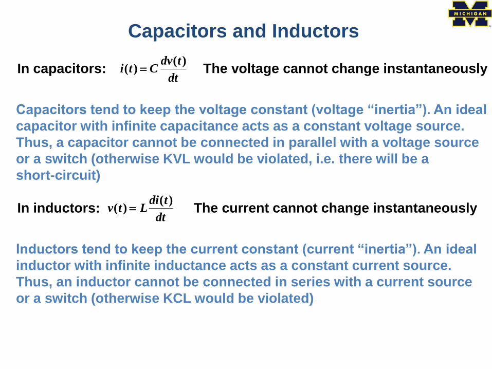
Capacitors and Inductors
In capacitors:dt
tdvCti
)()(
Capacitors tend to keep the voltage constant (voltage “inertia”). An ideal
capacitor with infinite capacitance acts as a constant voltage source.
Thus, a capacitor cannot be connected in parallel with a voltage source
or a switch (otherwise KVL would be violated, i.e. there will be a
short-circuit)
The voltage cannot change instantaneously
In inductors:
Inductors tend to keep the current constant (current “inertia”). An ideal
inductor with infinite inductance acts as a constant current source.
Thus, an inductor cannot be connected in series with a current source
or a switch (otherwise KCL would be violated)
The current cannot change instantaneouslydt
tdiLtv
)()(

Functionality – Switching Converters
• Common switching converters– In switching converters, load current and voltage is
largely determined by the operation of transistor switching
• The duty cycle of the switching will determine the mode each converter operate at various loads
– Continuous Mode» The inductor current will never fall to zero when the
switch is off» Smaller current peak during operation
– Discontinuous Mode» Inductor current will reach zero before the end of the
full duty cycle– Each mode has its advantages and disadvantages depending
on the switching converters. » In generally it’s how they change the frequency
response.
D is the duty cycle
Figure from Wikipedia

Functionality – Buck
– Continuous mode – Discontinuous mode
Common switching converters
Using buck converter as an example, you can see the pulses with a certain 𝑇𝑜𝑛/𝑇𝑂𝐹𝐹. This is the duty cycle of the transistor switching
When the transistor is on it also creates a reverse bias voltage (𝑉𝐶−𝑃) across the diode.

Functionality – Buck
– Continuous mode – Discontinuous mode
Common switching converters
As the switch is on there is current flow 𝐼𝑄 through the transistor
Current is a ramp because of the inductor
High 𝐼𝑄 peak also creates more stress on the transistor

Functionality – Buck
– Continuous mode – Discontinuous mode
Common switching converters
During the off time there is now forward bias current flowing through the diode from inductor discharging
Inductor is discharging so the current starts to ramp down

Functionality – Buck
– Continuous mode – Discontinuous mode
Common switching converters
The output now has a ripple to it and not desirable for controlling the converter
Instead of 𝐼𝑜 = 𝐼𝐿 , Io = ILavg, so when the feedback happens the control can
read a constant value
From the feedback the switching duty cycle is changed to keep the converter in a particular state.

Functionality – Buck
– Continuous mode – Discontinuous mode
Common switching converters
For buck converters we generally want to operate at continuous mode because 𝑉𝑜only depends on the duty cycle which makes it easier to control
There are many published paper that cover the subject, a good one ishttp://www.ti.com/lit/an/slva057/slva057.pdf

35
Examine the inductor current
Switch closed,
Switch open,
L
VV
dt
diVVv outinL
outinL
,
L
V
dt
diVv outL
outL
,
sec/ AL
VV outin
DT (1 − D)T
T
Imax
Imin
Iavg = Iout
From geometry, Iavg = Iout is halfway
between Imax and Iminsec/ A
L
Vout
ΔI
iL
Periodic – finishes
a period where it
started

36
Effect of raising and lowering Iout while
holding Vin, Vout, f, and L constant
iL
ΔI
ΔIRaise Iout
ΔI
Lower Iout
• ΔI is unchanged
• Lowering Iout moves the circuit toward discontinuous
operation

37
Effect of raising and lowering f while
holding Vin, Vout, Iout, and L constant
iL
Raise f
Lower f
• Slopes of iL are unchanged
• Lowering f increases ΔI and moves the circuit toward
discontinuous operation

38
iL
Effect of raising and lowering L while
holding Vin, Vout, Iout and f constant
Raise L
Lower L
• Lowering L increases ΔI and moves the circuit toward
discontinuous operation

Functionality – Switching Converters(again)
• Common switching converters– In switching converters, load current and voltage is
largely determined by the operation of transistor switching
• The duty cycle of the switching will determine the mode each converter operate at various loads
– Continuous Mode» The inductor current will never fall to zero when the
switch is off» Smaller current peak during operation
– Discontinuous Mode» Inductor current will reach zero before the end of the
full duty cycle– Each mode has its advantages and disadvantages depending
on the switching converters. » In generally it’s how they change the frequency
response.
D is the duty cycle
Figure from Wikipedia

Net effect—avoiding discontinuous mode
• Lower load current, lower inductance and lower switching frequency move us toward discontinuous mode.
There are pros and consto both modes, but onereal issue is that switchingbetween them can cause ringing on the inductor’s output.(See UT slides for why, has to do with parasiticcap in transistor and diode.

Boost (done a bit more quickly)

42
Vin
+Vout
–C
iC
IoutiinBuck converter iL
L
+ vL –
Boost converter
Vin
+Vout
–C
iC
IoutiiniL
L
+ vL –

43
Boost converter
This is a much more unforgiving circuit than the buck converter
Vin
+Vout
–C
iC
IoutiiniL
L
+ vL –
iD
• If the MOSFET gate driver sticks in the “on” position, then there
is a short circuit through the MOSFET – blow MOSFET!
• If the load is disconnected during operation, so that Iout = 0, then
L continues to push power to the right and very quickly charges
C up to a high value (250V) – blow diode and MOSFET!
• Before applying power be sure that a load is solidly connected
!

• On state– Current flows through the
transistor(least resistance)making the diode reverse bias and no 𝐼𝐷
– Inductor is charged in the process
• Off state– The energy discharged by the
inductor is superimposed to theinput, generating a higher output
Functionality – Boost
Generic boost schematic
Boost: on state
Boost: off stateSchematics from http://en.wikipedia.org/wiki/Boost_converter
D
VV in
out
1

Functionality – Switching Converters
– Continuous mode – Discontinuous mode
Common switching converters - Boost
From the timing diagram you can see this is very similar to the buck timing diagram with a difference in that 𝑉𝑖 only affects 𝑉𝑜 directly when the switch is off
Similar to buck, in continuous mode the output is control by the duty cycle.
But unfortunately, boost favor discontinuous mode, in continuous mode there is a complex second order characteristic in noise. Discontinuous mode removes the inductance noise, producing simpler response to compensate and control
Schematics from http://en.wikipedia.org/wiki/Boost_converter

• Common switching converters
– Buck-boost(inverting)• The baby of buck and boost…
• On state– Diode is reverse biased and the
inductor is charged but input and output is isolated from each other
» Creates more stress on the diode!
– 𝑉𝑜 is now the charged 𝑉𝑐 from off state but different polarity
• Off state– Inductor voltage reverses, passing
energy to the capacitor and load through forward biased diode
• Due to the characteristics of boost, buck-boost suffers the same problem. Therefore a discontinuous mode is favored
Functionality – Switching Converters
Generic buck- boost schematic
Buck-boost: on state
Buck-boost: off state
Schematics from http://en.wikipedia.org/wiki/Buck%E2%80%93boost_converter

• To give you a better idea of how duty cycle affect the output of each converter in continuous mode refer to the table below
– Each duty cycle equation is equal to the ratio of 𝑉𝑜𝑢𝑡
𝑉𝑖𝑛
– In discontinuous mode these equations are no longer true, but we will not discuss them here and they can also be found online
– More information on each of the switching converter can be found at http://www.nxp.com/documents/application_note/APPCHP2.pdfhttp://ecee.colorado.edu/copec/book/slides/Ch5slide.pdfhttp://www.ti.com/lit/an/slva057/slva057.pdf
Functionality – Switching Converters
Converters Duty cycle
Buck1
𝐷
Boost1
1 − 𝐷
Buck-boost(inverting)𝐷
1 − 𝐷

Picking converters
• Hopefully at this point you can start to see how much more complicated a switching converter is relative to a linear converter
– Every change made to the capacitor, inductor, transistor or diode will have an significant effect in not only the efficiency of each converter but also the life and way they operate
– Fortunately it won’t be the end of the world if you decide to use switching converters
• Using mic2168a, a controller for buck converter, as example. We can see not only do they provide information on the controller but also the external components needed for proper functionality (9pages!).
– ON semiconductor also provide a detailed published paper on both linear and switching regulator, covering the theory and design consideration needed.

• For those who aren’t as interested in all the technical details behind all this can refer to TI’s power management portal.
•
• You can just enter the parameters and TI will come up with recommendation
• Other companies also offer similar things so you’re not stuck with only TI– Try Micrel, Freescale or other brands as needed.
Picking converters

Efficiency of switchers
• It’s going to vary a lot.
– Depends on the converter,the output current, etc.
– Graph on the right is of a TPS5420 under reasonableconditions.
• Typically has only 18μA current whenyou shut it down (needs a control pin)
TPS5420

Stability
TPS5420

More stability


![Storage Fabric · 2017. 5. 7. · Erasure Coding in Windows Azure Storage [Huang, 2012] Exploit Point: 𝑃 1 𝑖 𝑢 ≫𝑃 [2 𝑖 𝑢 ] Solution: Construct Erasure Code Technique](https://img.pdfslide.us/doc/110x75/60056bc83d82b045d111d738/storage-2017-5-7-erasure-coding-in-windows-azure-storage-huang-2012-exploit.jpg)