Embed Size (px)
Citation preview
EECS 247 Lecture 19: Data Converters © 2006 H.K. Page 1
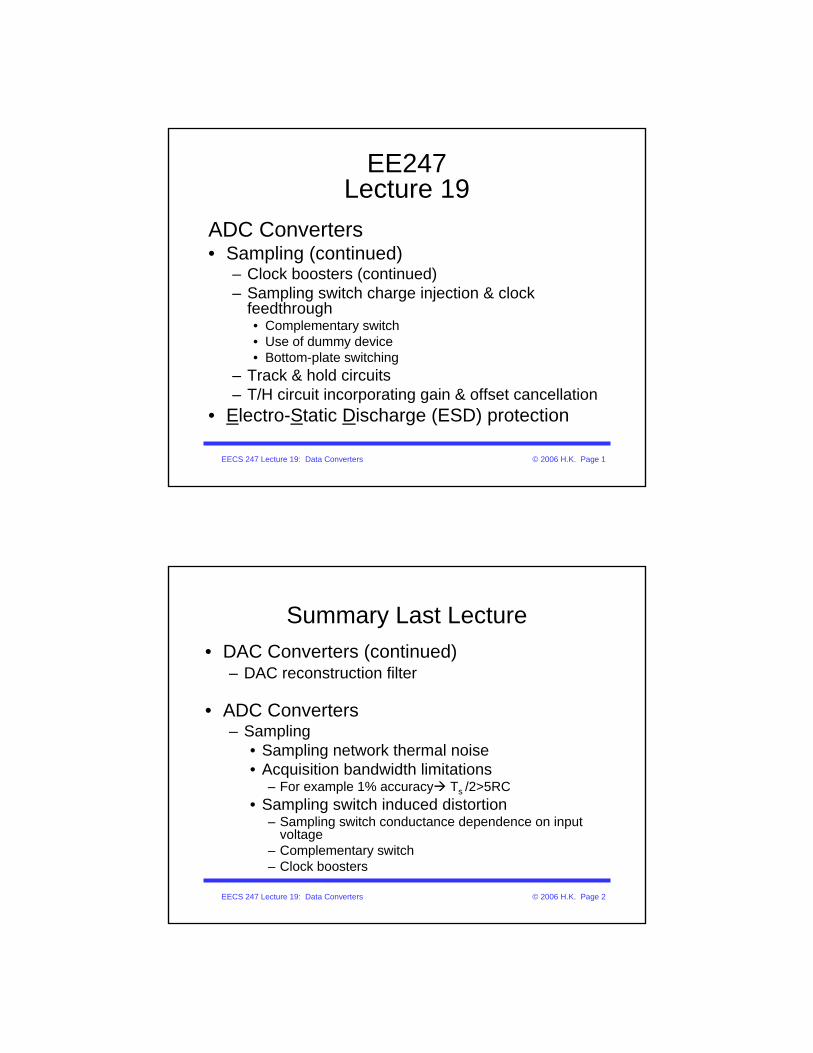
EE247Lecture 19
ADC Converters• Sampling (continued)
– Clock boosters (continued)– Sampling switch charge injection & clock
feedthrough• Complementary switch• Use of dummy device• Bottom-plate switching
– Track & hold circuits– T/H circuit incorporating gain & offset cancellation
• Electro-Static Discharge (ESD) protection
EECS 247 Lecture 19: Data Converters © 2006 H.K. Page 2
Summary Last Lecture• DAC Converters (continued)
– DAC reconstruction filter
• ADC Converters– Sampling
• Sampling network thermal noise• Acquisition bandwidth limitations
– For example 1% accuracy Ts /2>5RC• Sampling switch induced distortion
– Sampling switch conductance dependence on input voltage
– Complementary switch– Clock boosters
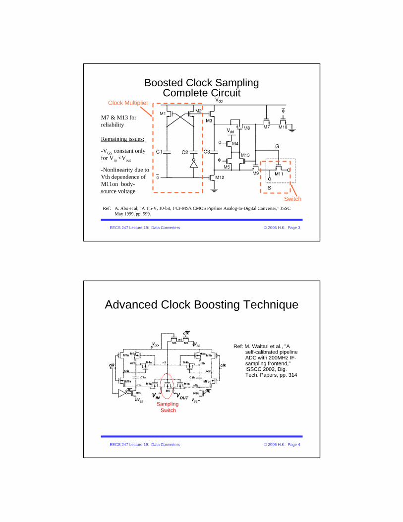
EECS 247 Lecture 19: Data Converters © 2006 H.K. Page 3
Boosted Clock Sampling Complete Circuit
Ref: A. Abo et al, “A 1.5-V, 10-bit, 14.3-MS/s CMOS Pipeline Analog-to-Digital Converter,” JSSC May 1999, pp. 599.
Clock Multiplier
Switch
M7 & M13 for reliability
Remaining issues:
-VGS constant only for Vin <Vout
-Nonlinearity due to Vth dependence of M11on body-source voltage
EECS 247 Lecture 19: Data Converters © 2006 H.K. Page 4
Advanced Clock Boosting Technique
Ref: M. Waltari et al., "A self-calibrated pipeline ADC with 200MHz IF-sampling frontend," ISSCC 2002, Dig. Tech. Papers, pp. 314
Sampling Switch
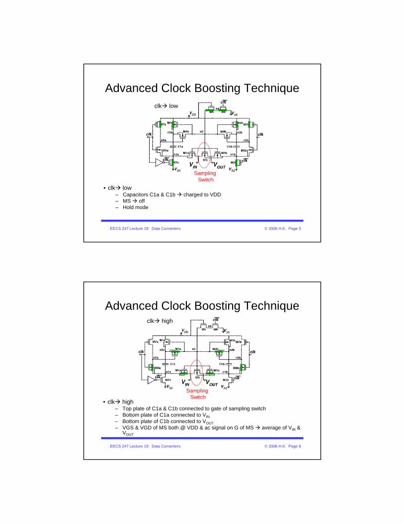
EECS 247 Lecture 19: Data Converters © 2006 H.K. Page 5
Advanced Clock Boosting Technique
• clk low– Capacitors C1a & C1b charged to VDD– MS off– Hold mode
Sampling Switch
clk low
EECS 247 Lecture 19: Data Converters © 2006 H.K. Page 6
Advanced Clock Boosting Technique
Sampling Switch
• clk high– Top plate of C1a & C1b connected to gate of sampling switch– Bottom plate of C1a connected to VIN– Bottom plate of C1b connected to VOUT– VGS & VGD of MS both @ VDD & ac signal on G of MS average of VIN &
VOUT
clk high

EECS 247 Lecture 19: Data Converters © 2006 H.K. Page 7
Advanced Clock Boosting Technique
• Gate tracks average of input and output, reduces effect of I·R drop at high frequencies
• Bulk also tracks signal ⇒ reduced body effect (technology used allows connecting bulk to S)
• Reported measured SFDR = 76.5dB at fin=200MHz
Ref: M. Waltari et al., "A self-calibrated pipeline ADC with 200MHz IF-sampling frontend," ISSCC 2002, Dig. Tech. Papers, pp. 314
Sampling Switch
EECS 247 Lecture 19: Data Converters © 2006 H.K. Page 8
Constant Conductance Switch
Ref: H. Pan et al., "A 3.3-V 12-b 50-MS/s A/D converter in 0.6um CMOS with over 80-dB SFDR," IEEE J. Solid-State Circuits, pp. 1769-1780, Dec. 2000
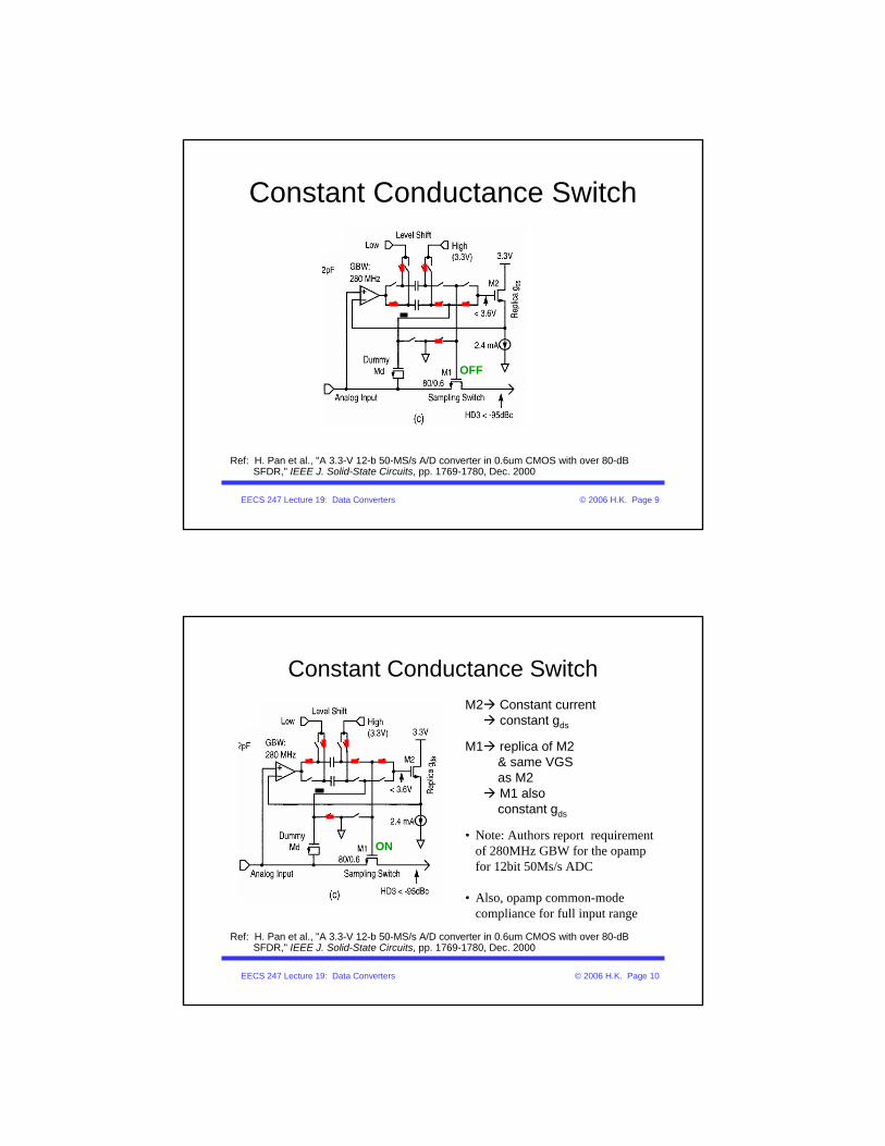
EECS 247 Lecture 19: Data Converters © 2006 H.K. Page 9
Constant Conductance Switch
Ref: H. Pan et al., "A 3.3-V 12-b 50-MS/s A/D converter in 0.6um CMOS with over 80-dB SFDR," IEEE J. Solid-State Circuits, pp. 1769-1780, Dec. 2000
OFF
EECS 247 Lecture 19: Data Converters © 2006 H.K. Page 10
Constant Conductance Switch
Ref: H. Pan et al., "A 3.3-V 12-b 50-MS/s A/D converter in 0.6um CMOS with over 80-dB SFDR," IEEE J. Solid-State Circuits, pp. 1769-1780, Dec. 2000
ON
M2 Constant currentconstant gds
M1 replica of M2 & same VGSas M2M1 alsoconstant gds
• Note: Authors report requirement of 280MHz GBW for the opamp for 12bit 50Ms/s ADC
• Also, opamp common-mode compliance for full input range
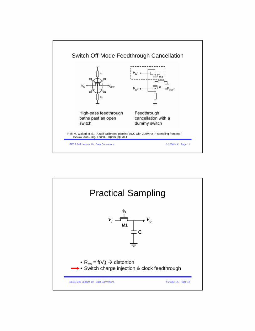
EECS 247 Lecture 19: Data Converters © 2006 H.K. Page 11
Switch Off-Mode Feedthrough Cancellation
Ref: M. Waltari et al., "A self-calibrated pipeline ADC with 200MHz IF-sampling frontend," ISSCC 2002, Dig. Techn. Papers, pp. 314
EECS 247 Lecture 19: Data Converters © 2006 H.K. Page 12
Practical Sampling
Vo
CM1
φ1
• Rsw = f(Vi) distortion• Switch charge injection & clock feedthrough
Vi

EECS 247 Lecture 19: Data Converters © 2006 H.K. Page 13
Sampling Switch Charge Injection & Clock FeedthroughSwitching from Track to Hold
Vi VO
Cs
M1
VG
• First assume Vi is a DC voltage• When switch turns off offset voltage induced on Cs• Why?
VG
t
VH
Vi
VL
Vi +Vth
VO
Vi
toff
ΔV
t
EECS 247 Lecture 19: Data Converters © 2006 H.K. Page 14
SamplingSwitch Charge Injection
• Channel distributed RC network formed between G,S, and D• Channel to substrate junction capacitance distributed & voltage dependant• Drain/Source junction capacitors to substrate voltage dependant• Over-lap capacitance Cov = LDxWxCox
’ associated with G-S & G-D overlap
MOS xtor operating in triode regionCross section view
Distributed channel resistance & gate & junction capacitances
S
G
D
B
LD
L
Cov Cov
Cjdb
Cjsb
CHOLD
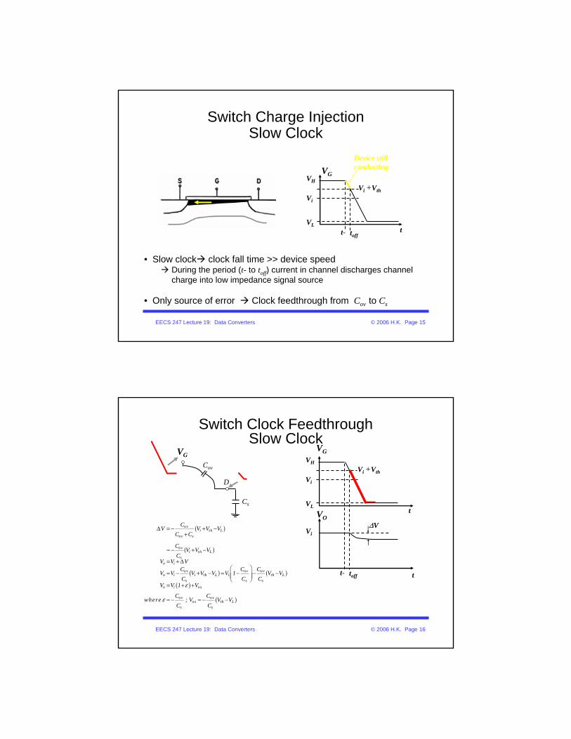
EECS 247 Lecture 19: Data Converters © 2006 H.K. Page 15
Switch Charge Injection Slow Clock
• Slow clock clock fall time >> device speed During the period (t- to toff) current in channel discharges channel charge into low impedance signal source
• Only source of error Clock feedthrough from Cov to Cs
VG
t
VH
Vi
VL
Vi +Vth
tofft-
Device still conducting
EECS 247 Lecture 19: Data Converters © 2006 H.K. Page 16
Switch Clock Feedthrough Slow Clock
VG
t
VH
Vi
VL
Vi +Vth
VO
Vi
toff
ΔV
t
D
Cov
VG
( )
( )
( ) ( )
( )
( )
ovi th L
ov s
ovi th L
so i
ov ov ovo i i th L i th L
s s so i os
ov ovos th L
s s
CV V V V
C C
CV V V
CV V V
C C CV V V V V V 1 V V
C C CV V 1 V
C Cwhere ; V V V
C C
ε
ε
Δ = − + −+
≈ − + −
= + Δ⎛ ⎞
= − + − = − − −⎜ ⎟⎜ ⎟⎝ ⎠
= + +
= − = − −
t-
Cs
EECS 247 Lecture 19: Data Converters © 2006 H.K. Page 17
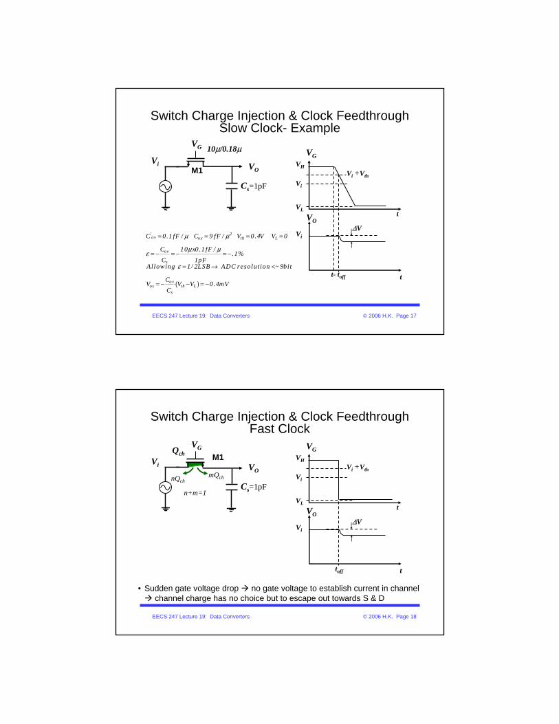
Switch Charge Injection & Clock Feedthrough Slow Clock- Example
( )
' 2ov ox th L
ov
s
ovos th L
s
C 0.1 fF / C 9 fF / V 0.4V V 0
C 10 x0.1 fF /.1%
C 1pFAllowing 1/ 2LSB ADC resolut ion ~ 9bit
CV V V 0.4mV
C
μ μ
μ με
ε
= = = =
= − = − = −
= → <
= − − = −
VG
t
VH
Vi
VL
Vi +Vth
VO
Vi
toff
ΔV
t
Vi VO
Cs=1pF
M1
VG 10μ/0.18μ
t-
EECS 247 Lecture 19: Data Converters © 2006 H.K. Page 18
Switch Charge Injection & Clock Feedthrough Fast Clock
VG
t
VH
Vi
VL
Vi +Vth
VO
Vi
toff
ΔV
t
Vi VO
Cs=1pF
M1VG
• Sudden gate voltage drop no gate voltage to establish current in channel channel charge has no choice but to escape out towards S & D
Qch
mQchnQch
n+m=1
EECS 247 Lecture 19: Data Converters © 2006 H.K. Page 19
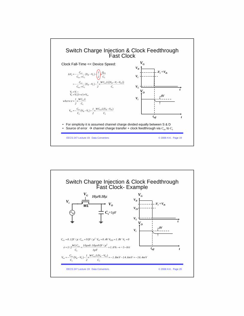
( )
( ) ( )( )
( )
( ) ( )
ov cho H L
ov s s
ox H i thovH L
ov s s
o io i os
ox
s
ov ox H thos H L
s s
C 1 QV V V
C C 2 C
WC L V V VC 1V V
C C 2 C
V VV V 1 V
1 WC Lwhere
2 C
C 1 WC L V VV V V
C 2 C
ε
ε
Δ = − − − ×+
− −≈ − − − ×
+
= −= + +
= ×
−= − − − ×
• For simplicity it is assumed channel charge divided equally between S & D • Source of error channel charge transfer + clock feedthrough via Cov to Cs
VG
t
VH
Vi
VL
Vi +Vth
VO
Vi
toff
ΔV
t
Switch Charge Injection & Clock FeedthroughFast Clock
Clock Fall-Time << Device Speed:
EECS 247 Lecture 19: Data Converters © 2006 H.K. Page 20
Switch Charge Injection & Clock FeedthroughFast Clock- Example
( ) ( )
2ov ox th DD L
2ox
s
ov ox H thos H L
s s
C 0.1 fF / C 9 fF / V 0.4V V 1.8V V 0
WLC 10 x0.18 x9 fF /1/ 2 1.6% ~ 5 bit
C 1pF
C 1 WC L V VV V V 1.8mV 14.6mV 16.4mV
C 2 C
μ μ
μ μ με
= = = = =
= = = → −
−= − − − × = − − = −
Vi VO
Cs=1pF
M1
VG 10μ/0.18μ VG
t
VH
VIN
VL
Vi +Vth
VO
Vi
toff
ΔV
t
EECS 247 Lecture 19: Data Converters © 2006 H.K. Page 21
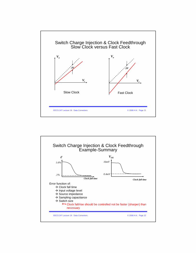
Vo
ΔV
Vi
Switch Charge Injection & Clock FeedthroughSlow Clock versus Fast Clock
Slow Clock
Vo
ΔV
Vi
Fast Clock
EECS 247 Lecture 19: Data Converters © 2006 H.K. Page 22
Switch Charge Injection & Clock FeedthroughExample-Summary
Error function of:Clock fall time Input voltage level Source impedance Sampling capacitanceSwitch size
Clock fall/rise should be controlled not be faster (sharper) than necessary
Clock fall time
ε VOS
Clock fall time
1.6%
.1%
16mV
0.4mV
EECS 247 Lecture 19: Data Converters © 2006 H.K. Page 23
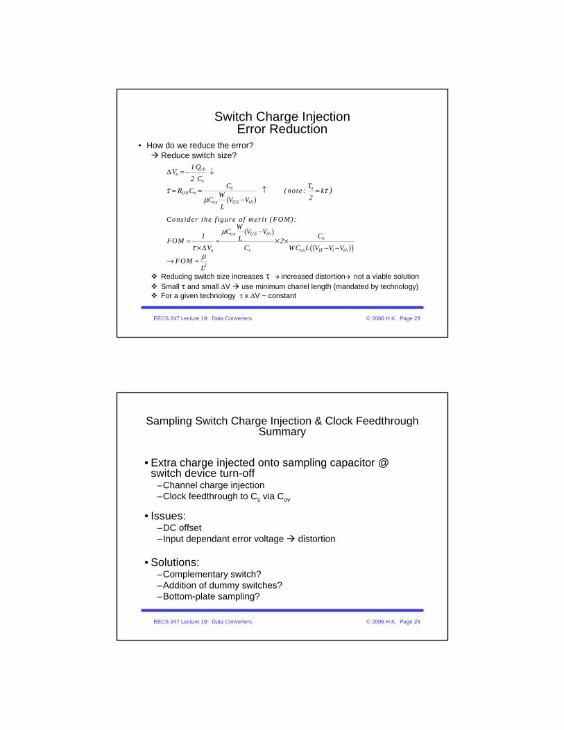
Switch Charge InjectionError Reduction
( )
( )
( )( )
cho
ss s
ON s
ox GS th
ox GS ths
o s ox H i th
2
1 QV
2 CC T
R C ( note : kW 2C V VL
Consider the f igure of meri t (FOM):W
C V V1 CLFOM 2V C WC L V V V
FOML
)μ
μ
μ
τ τ
τ
Δ = − ↓
= = ↑ =−
−= ≈ ×
Δ − −
→ ≈
××
• How do we reduce the error? Reduce switch size?
Reducing switch size increases τ increased distortion not a viable solutionSmall τ and small ΔV use minimum chanel length (mandated by technology)For a given technology τ x ΔV ~ constant
EECS 247 Lecture 19: Data Converters © 2006 H.K. Page 24
Sampling Switch Charge Injection & Clock FeedthroughSummary
• Extra charge injected onto sampling capacitor @ switch device turn-off
–Channel charge injection–Clock feedthrough to Cs via Cov
• Issues:–DC offset–Input dependant error voltage distortion
• Solutions:–Complementary switch?–Addition of dummy switches?–Bottom-plate sampling?
EECS 247 Lecture 19: Data Converters © 2006 H.K. Page 25
Switch Charge InjectionComplementary Switch
• In slow clock case if area of n & p devices widths are equal (Wn=Wp) effect of overlap capacitor for n & p devices to first order cancel (cancellation accuracy depends on matching of n & p width and ΔL)
• Since in CMOS technologies μn~2.5μp choice of Wn=Wp not optimal from linearity perspective (Wp>Wn preferable)
φ1φ1B
φ1
φ1B
VG
t
VH
Vi
VL
φ1 φ1B
EECS 247 Lecture 19: Data Converters © 2006 H.K. Page 26
Switch Charge Injection Complementary Switch
Fast Clock
• In fast clock case To 1st order, offset due to overlap caps
cancelled for equal device widthInput voltage dependant error worse!
φ1
φ1B
VG
t
VH
Vi
VL
( )
( )
( )
ch n n ox n H i th n
th pch p p ox p i L
ch pch no
s s
o i os
n ox n p ox p
s
Q W C L V V V
VQ W C L V V
Q1 QV
2 C C
V V 1 V
W C L W C L12 C
ε
ε
− −
−−
−−
= − −
= − −
⎛ ⎞Δ ≈ − −⎜ ⎟⎜ ⎟
⎝ ⎠
= + +
+≈ ×

EECS 247 Lecture 19: Data Converters © 2006 H.K. Page 27
Switch Charge InjectionDummy Switch
Vi
VO
Cs
t
VH
Vi
VL
VG VGB
WM2=1/2WM1
VG VGB
M1 M2
M 1 M 11 ch ov
M 2 M 22 ch ov
M 2 M 1 2 1
1Q Q Q
2Q Q 2Q
1For W W Q Q
2
≈ +
≈ +
= → = −
Q1 Q2
EECS 247 Lecture 19: Data Converters © 2006 H.K. Page 28
Switch Charge InjectionDummy Switch
Vi
VO
Cs
t
VH
Vi
VL
VG VGB
• Dummy switch same L as main switch but half W • Main device clock goes low, dummy device gate goes high dummy
switch acquires same amount of channel charge main switch needs to lose
• Effective only if exactly half of the charge transferred to M2 (depends on input/output node impedance) and requires good matching between clock fall/rise
WM2=1/2WM1
VG VGB
M1 M2
Q1 Q2
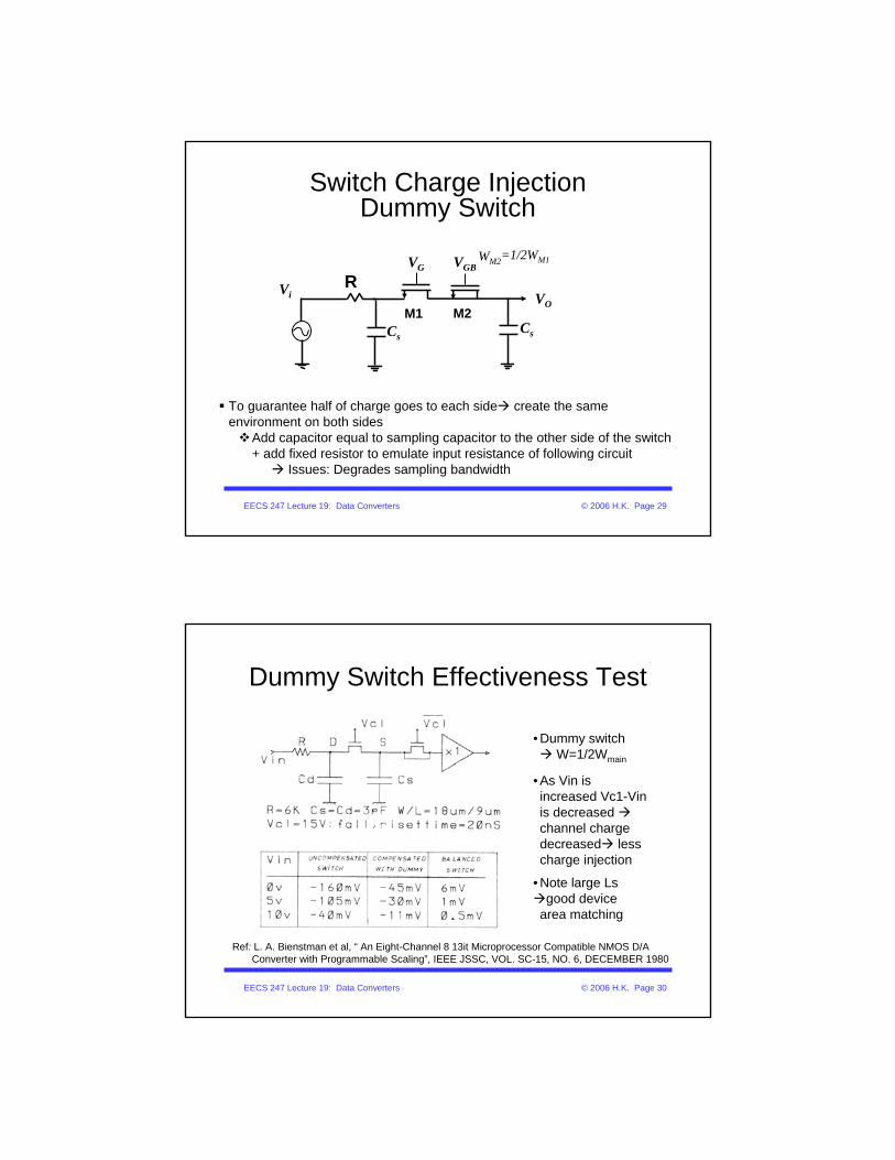
EECS 247 Lecture 19: Data Converters © 2006 H.K. Page 29
Switch Charge InjectionDummy Switch
Vi VOM1
VG
M2
VGB
To guarantee half of charge goes to each side create the same environment on both sides
Add capacitor equal to sampling capacitor to the other side of the switch + add fixed resistor to emulate input resistance of following circuit
Issues: Degrades sampling bandwidth
CsCs
RWM2=1/2WM1
EECS 247 Lecture 19: Data Converters © 2006 H.K. Page 30
Dummy Switch Effectiveness Test
Ref: L. A. Bienstman et al, “ An Eight-Channel 8 13it Microprocessor Compatible NMOS D/A Converter with Programmable Scaling”, IEEE JSSC, VOL. SC-15, NO. 6, DECEMBER 1980
• Dummy switch W=1/2Wmain
• As Vin is increased Vc1-Vin is decreased channel charge decreased less charge injection
• Note large Lsgood device
area matching

EECS 247 Lecture 19: Data Converters © 2006 H.K. Page 31
Switch Charge InjectionDifferential Sampling
Vi+
VO+
Vi-
VO-
• To 1st order, offset terms cancel• Note gain error ε still about the same• Has the advantage of better immunity to
noise coupling and cancellation of even order harmonics
φ
Cs
Cs
( )( )
( ) ( )
o o od i i id
o o i ioc ic
o i 1 os1
o i 2 os2
1 2od id id 1 2 ic os1 os2
V V V V V V
V V V VV V
2 2V V 1 V
V V 1 V
V V V V V V2
ε
ε
ε ε ε ε
+ − + −
+ − + −
+ +
− −
− = − =
+ += =
= + +
= + +
+= + + − + −
EECS 247 Lecture 19: Data Converters © 2006 H.K. Page 32
Switch Charge InjectionBottom Plate Sampling
• Switches M2 opened slightly earlier compared to M1Injected charge by the opening of M2 is constant & eliminated when
used differentially
• Since Cs bottom plate open when M1 opened no charge injected on Cs
φ1aVH
VL
t
φ1bVi
VO
M1
φ1b
φ1a M2
Cs
EECS 247 Lecture 19: Data Converters © 2006 H.K. Page 33
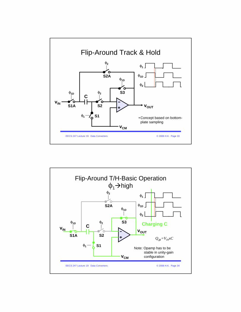
Flip-Around Track & Hold
vIN vOUT
C
S1A
φ1D
S2
φ2
S2A
φ2
S3
φ1D
φ1 S1
vCM
• Concept based on bottom-plate sampling
φ1
φ2
φ1D
EECS 247 Lecture 19: Data Converters © 2006 H.K. Page 34
Flip-Around T/H-Basic Operationφ1 high
vIN vOUT
C
S1A
φ1D
S2
φ2
S2A
φ2
S3
φ1D
φ1 S1
vCM
Charging C
φ1
φ1D
φ2
Note: Opamp has to be stable in unity-gain configuration
Qφ1=VINxC
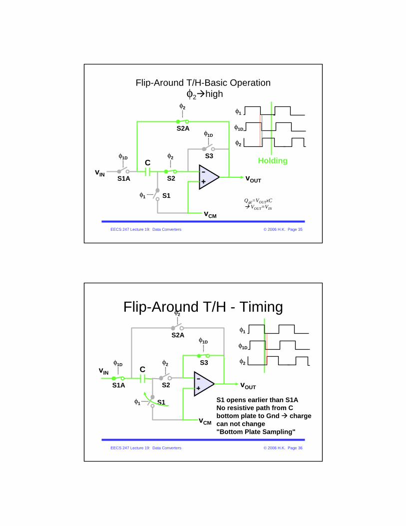
EECS 247 Lecture 19: Data Converters © 2006 H.K. Page 35
Flip-Around T/H-Basic Operationφ2 high
vIN vOUT
C
S1A
φ1D
S2
φ2
S2A
φ2
S3
φ1D
φ1 S1
vCM
Holding
φ1
φ2
φ1D
Qφ2=VOUTxCVOUT=VIN
EECS 247 Lecture 19: Data Converters © 2006 H.K. Page 36
Flip-Around T/H - Timing
S1 opens earlier than S1ANo resistive path from C bottom plate to Gnd charge can not change"Bottom Plate Sampling"
vIN
vOUT
C
S1A
φ1D
S2
φ2
S2A
φ2
S3
φ1D
φ1 S1
vCM
φ1
φ2
φ1D

EECS 247 Lecture 19: Data Converters © 2006 H.K. Page 37
Charge Injection• At the instant of transitioning from track to hold
mode, some of the charge stored in sampling switch S1 is dumped onto C
• With "Bottom Plate Sampling", only charge injection component due to opening of S1 and is to first-order independent of vIN– Only a dc offset is added This dc offset can be
removed with a differential architecture
EECS 247 Lecture 19: Data Converters © 2006 H.K. Page 38
Flip-Around T/H
vIN vOUT
C
S1A
φ1D
S2
φ2
S2A
φ2
S3
φ1D
φ1 S1
vCM
Constant switch VGSto minimize distortion
Note: Among all switches only S1A & S2A experience full input voltage swing
φ1
φ2
φ1D
EECS 247 Lecture 19: Data Converters © 2006 H.K. Page 39
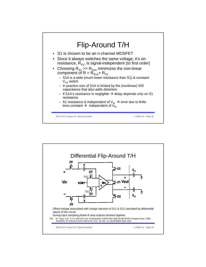
Flip-Around T/H• S1 is chosen to be an n-channel MOSFET• Since it always switches the same voltage, it’s on-
resistance, RS1, is signal-independent (to first order) • Choosing RS1 >> RS1A minimizes the non-linear
component of R = RS1A+ RS1– S1A is a wide (much lower resistance than S1) & constant
VGS switch– In practice size of S1A is limited by the (nonlinear) S/D
capacitance that also adds distortion– If S1A’s resistance is negligible delay depends only on S1
resistance– S1 resistance is independent of VIN error due to finite
time-constant independent of VIN
EECS 247 Lecture 19: Data Converters © 2006 H.K. Page 40
Differential Flip-Around T/H
Ref: W. Yang, et al. “A 3-V 340-mW 14-b 75-Msample/s CMOS ADC With 85-dB SFDR at Nyquist Input,” IEEE JOURNAL OF SOLID-STATE CIRCUITS, VOL. 36, NO. 12, DECEMBER 2001 1931
Offset voltage associated with charge injection of S11 & S12 cancelled by differential nature of the circuitDuring input sampling phase amp outputs shorted together
S11
S12
EECS 247 Lecture 19: Data Converters © 2006 H.K. Page 41
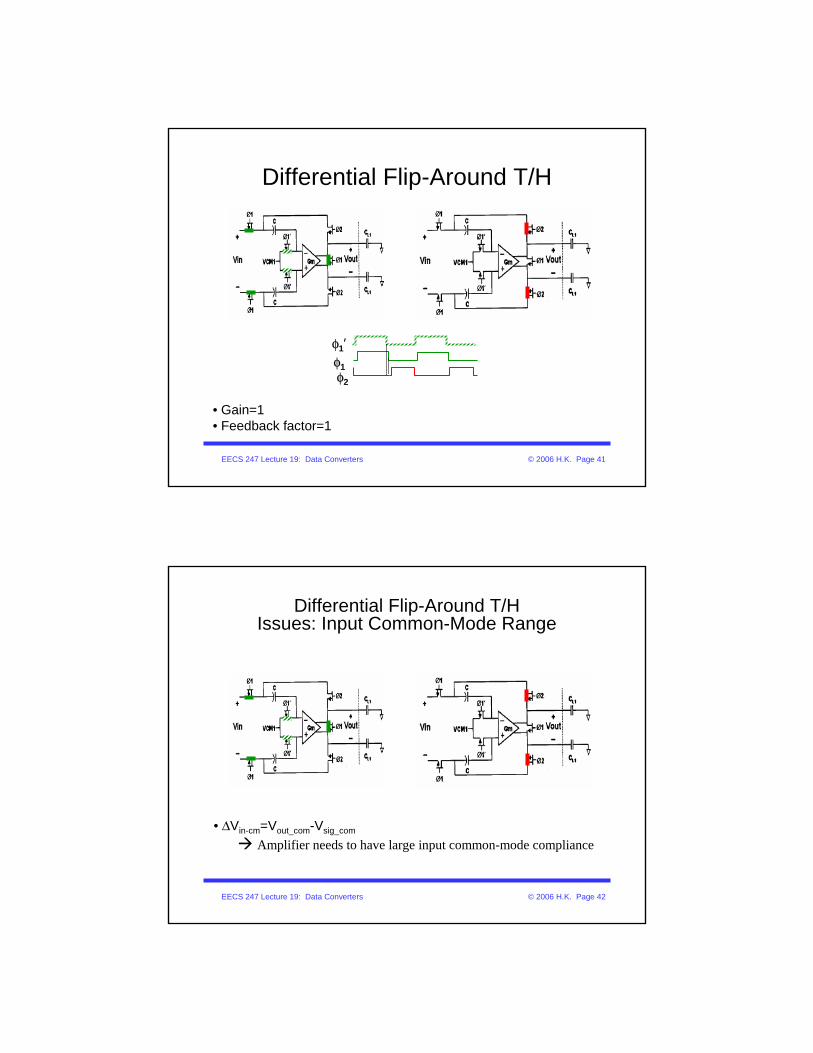
Differential Flip-Around T/H
• Gain=1• Feedback factor=1
φ1’φ1φ2
EECS 247 Lecture 19: Data Converters © 2006 H.K. Page 42
Differential Flip-Around T/HIssues: Input Common-Mode Range
• ΔVin-cm=Vout_com-Vsig_com
Amplifier needs to have large input common-mode compliance
EECS 247 Lecture 19: Data Converters © 2006 H.K. Page 43
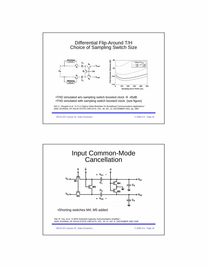
Differential Flip-Around T/HChoice of Sampling Switch Size
Ref: K. Vleugels et al, “A 2.5-V Sigma–Delta Modulator for Broadband Communications Applications “IEEE JOURNAL OF SOLID-STATE CIRCUITS, VOL. 36, NO. 12, DECEMBER 2001, pp. 1887
•THD simulated w/o sampling switch boosted clock -45dB•THD simulated with sampling switch boosted clock (see figure)
EECS 247 Lecture 19: Data Converters © 2006 H.K. Page 44
Input Common-Mode Cancellation
Ref: R. Yen, et al. “A MOS Switched-Capacitor Instrumentation Amplifier,”IEEE JOURNAL OF SOLID-STATE CIRCUITS, VOL. SC-17, NO. 6,, DECEMBER 1982 1008
•Shorting switches M4, M5 added
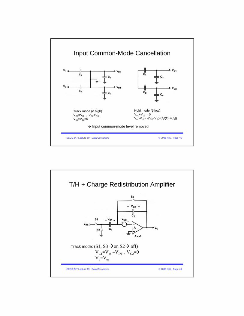
EECS 247 Lecture 19: Data Converters © 2006 H.K. Page 45
Input Common-Mode Cancellation
Track mode (φ high)VC1=VI1 , VC2=VI2Vo1=Vo2=0
Hold mode (φ low)Vo1+Vo2 =0Vo1-Vo2= -(VI1-VI2)(C1/(C1+C3))
Input common-mode level removed
EECS 247 Lecture 19: Data Converters © 2006 H.K. Page 46
T/H + Charge Redistribution Amplifier
Track mode: (S1, S3 on S2 off)VC1=Vos –VIN , VC2=0Vo=Vos

EECS 247 Lecture 19: Data Converters © 2006 H.K. Page 47
T/H + Charge Redistribution AmplifierHold Mode
Hold/amplify mode (S1, S3 off S2 on)
Offset NOT cancelled, but not amplifiedInput-referred offset =(C2/C1) x VOS, & C2<C1
2
1
2
EECS 247 Lecture 19: Data Converters © 2006 H.K. Page 48
T/H & Input Difference Amplifier
Sample mode (S1, S3 on S2 off)VC1=Vos –VI1 , VC2=0Vo=Vos
EECS 247 Lecture 19: Data Converters © 2006 H.K. Page 49
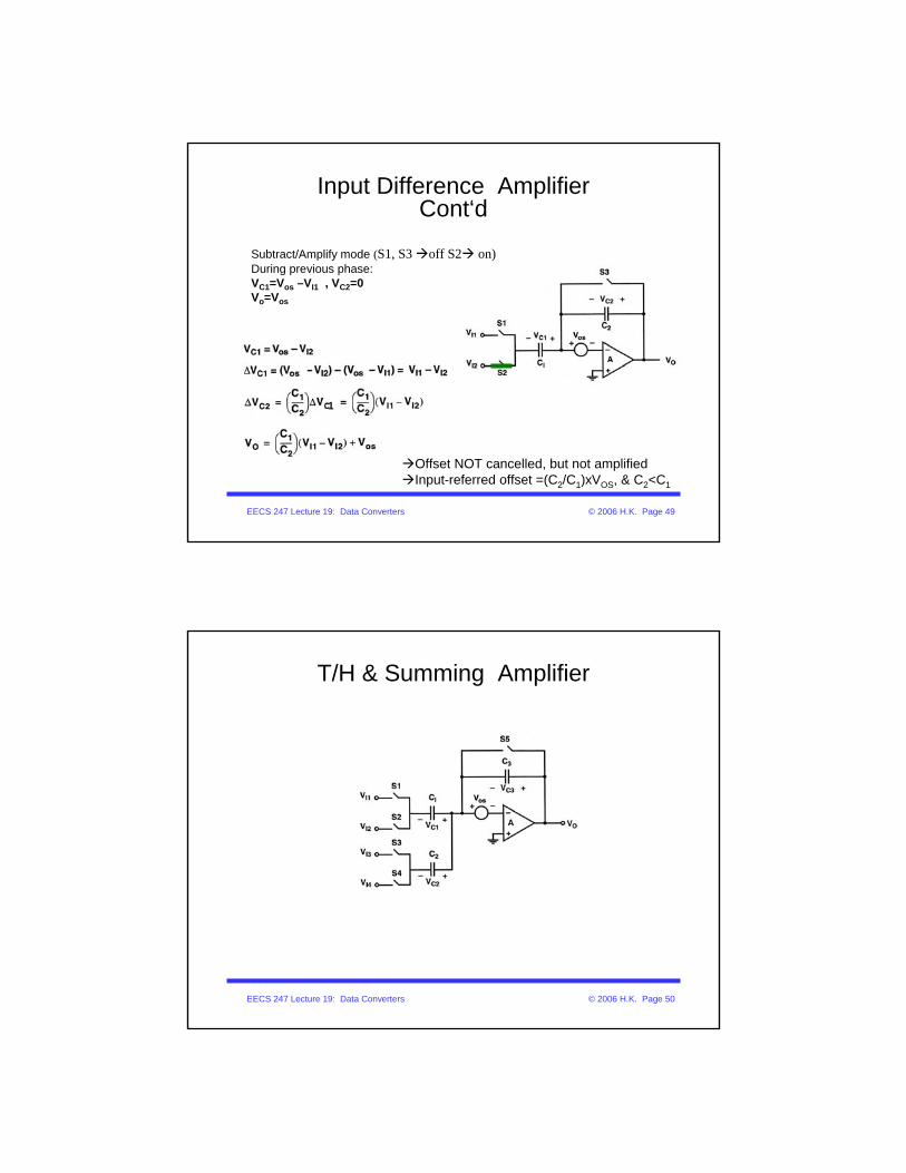
Input Difference AmplifierCont‘d
Subtract/Amplify mode (S1, S3 off S2 on)During previous phase:VC1=Vos –VI1 , VC2=0Vo=Vos
1
Offset NOT cancelled, but not amplifiedInput-referred offset =(C2/C1)xVOS, & C2<C1
EECS 247 Lecture 19: Data Converters © 2006 H.K. Page 50
T/H & Summing Amplifier
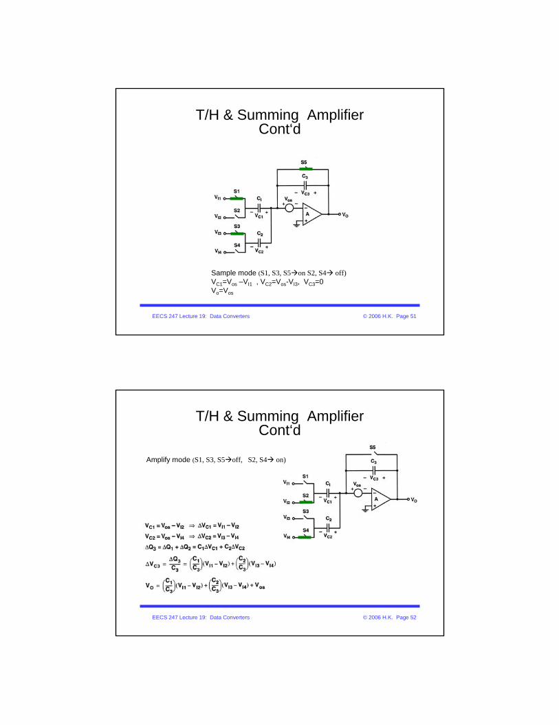
EECS 247 Lecture 19: Data Converters © 2006 H.K. Page 51
T/H & Summing AmplifierCont‘d
Sample mode (S1, S3, S5 on S2, S4 off)VC1=Vos –VI1 , VC2=Vos-VI3, VC3=0Vo=Vos
EECS 247 Lecture 19: Data Converters © 2006 H.K. Page 52
T/H & Summing AmplifierCont‘d
Amplify mode (S1, S3, S5 off, S2, S4 on)
3
EECS 247 Lecture 19: Data Converters © 2006 H.K. Page 53
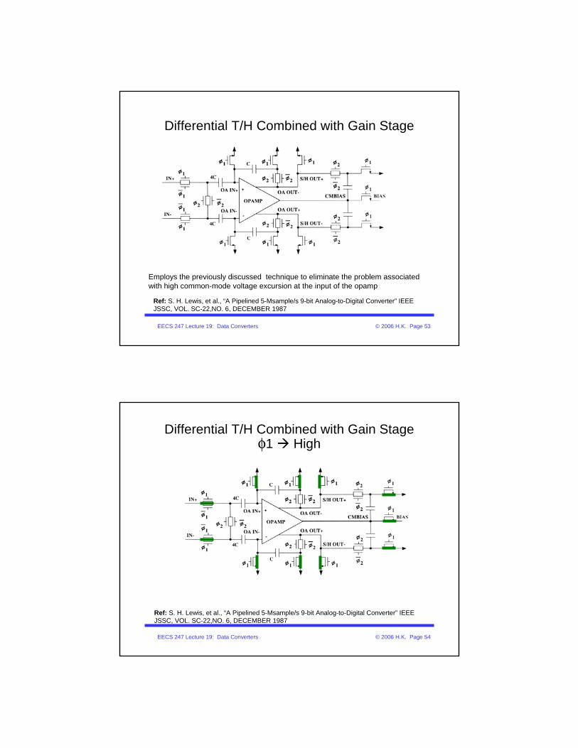
Differential T/H Combined with Gain Stage
Ref: S. H. Lewis, et al., “A Pipelined 5-Msample/s 9-bit Analog-to-Digital Converter” IEEE JSSC, VOL. SC-22,NO. 6, DECEMBER 1987
Employs the previously discussed technique to eliminate the problem associated with high common-mode voltage excursion at the input of the opamp
EECS 247 Lecture 19: Data Converters © 2006 H.K. Page 54
Ref: S. H. Lewis, et al., “A Pipelined 5-Msample/s 9-bit Analog-to-Digital Converter” IEEE JSSC, VOL. SC-22,NO. 6, DECEMBER 1987
Differential T/H Combined with Gain Stageφ1 High

EECS 247 Lecture 19: Data Converters © 2006 H.K. Page 55
Ref: S. H. Lewis, et al., “A Pipelined 5-Msample/s 9-bit Analog-to-Digital Converter” IEEE JSSC, VOL. SC-22,NO. 6, DECEMBER 1987
• Gain=4C/C=4• Input voltage common-mode level removed opamp can have low CMRR• Amplifier offset NOT removed
Differential T/H Combined with Gain Stage
EECS 247 Lecture 19: Data Converters © 2006 H.K. Page 56
Ref: H. Ohara, et al., "A CMOS programmable self-calibrating 13-bit eight-channel data acquisition peripheral," IEEE Journal of Solid-State Circuits, vol. 22, pp. 930 - 938, December 1987.
• Operation during offset cancellation phase shown• Auxilary inputs added with Amain/Aaux.=10• During offset cancellation phase:
•Aux. amp configured in unity-gain mode: Vout=Vosmain offset stored
on CAZ & canceled
Differential T/H Including Offset Cancellation
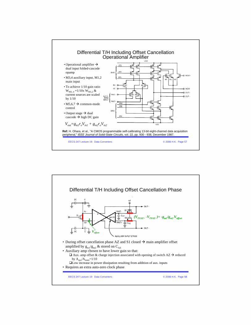
EECS 247 Lecture 19: Data Converters © 2006 H.K. Page 57
Differential T/H Including Offset CancellationOperational Amplifier
Ref: H. Ohara, et al., "A CMOS programmable self-calibrating 13-bit eight-channel data acquisition peripheral," IEEE Journal of Solid-State Circuits, vol. 22, pp. 930 - 938, December 1987.
• Operational amplifier dual input folded-cascode opamp
• M3,4 auxiliary input, M1,2 main input
• To achieve 1/10 gain ratio WM3, 4 =1/10x WM1,2 & current sources are scaled by 1/10
• M5,6,7 common-mode control
• Output stage dual cascode high DC gain
Vout=gm1roVin1 + gm2roVin2
EECS 247 Lecture 19: Data Converters © 2006 H.K. Page 58
• During offset cancellation phase AZ and S1 closed main amplifier offset amplified by gm1/gm2 & stored on CAZ
• Auxiliary amp chosen to have lower gain so that:Aux. amp offset & charge injection associated with opening of switch AZ reduced
by Aaux/Amain=1/10Low increase in power dissipation resulting from addition of aux. inputs
• Requires an extra auto-zero clock phase
Differential T/H Including Offset Cancellation Phase
Voffset
+
-(VINAZ+ -VINAZ- )= -gm1/gm2 Voffset
EECS 247 Lecture 19: Data Converters © 2006 H.K. Page 59
ESD ProtectionADC Architectures
EECS 247 Lecture 19: Data Converters © 2006 H.K. Page 60
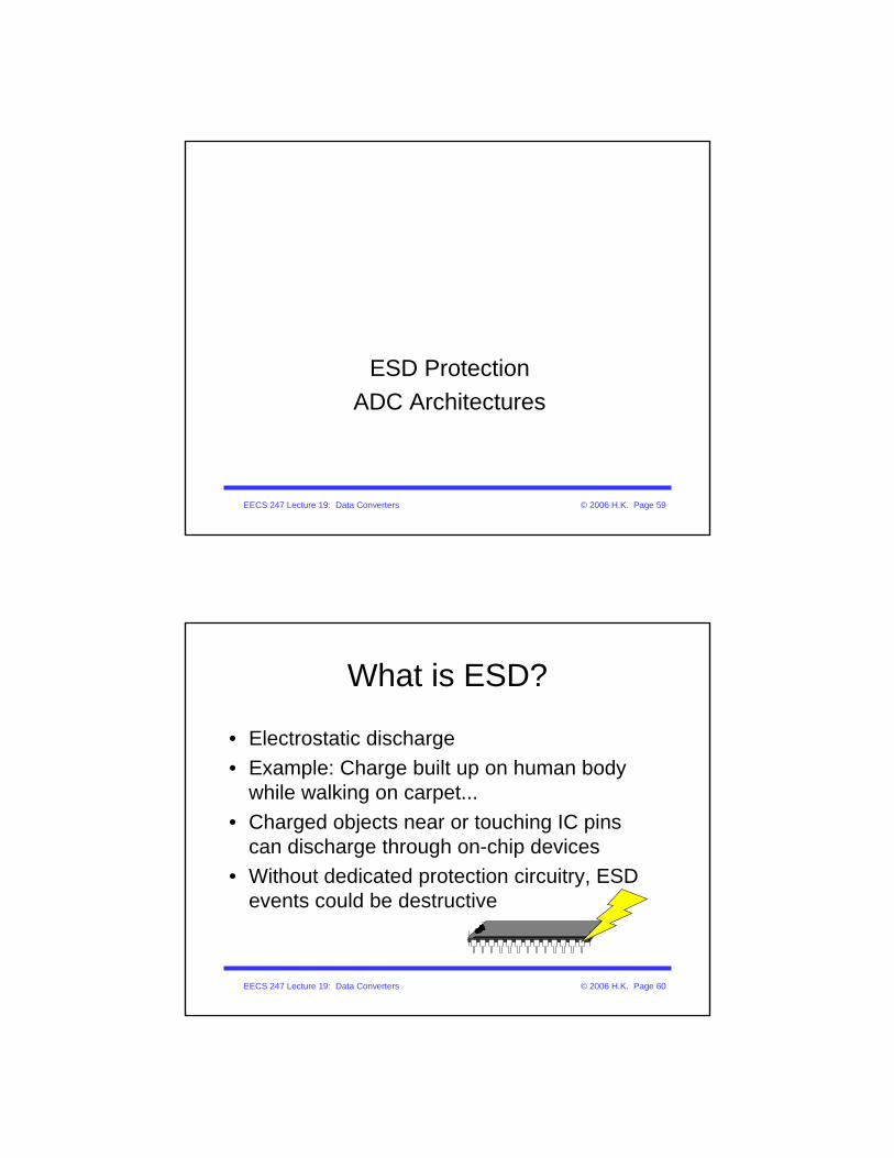
What is ESD?
• Electrostatic discharge• Example: Charge built up on human body
while walking on carpet...• Charged objects near or touching IC pins
can discharge through on-chip devices• Without dedicated protection circuitry, ESD
events could be destructive
EECS 247 Lecture 19: Data Converters © 2006 H.K. Page 61
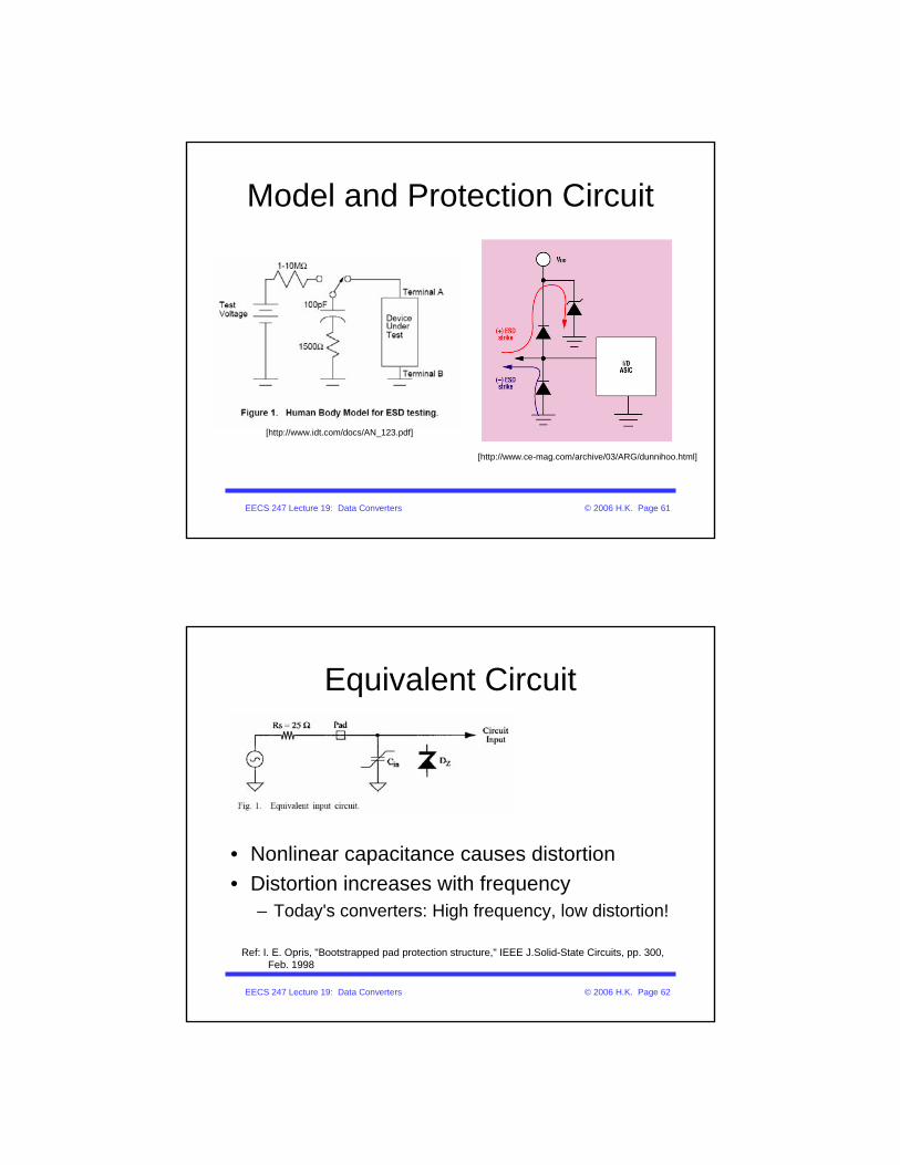
Model and Protection Circuit
[http://www.ce-mag.com/archive/03/ARG/dunnihoo.html]
[http://www.idt.com/docs/AN_123.pdf]
EECS 247 Lecture 19: Data Converters © 2006 H.K. Page 62
Equivalent Circuit
• Nonlinear capacitance causes distortion• Distortion increases with frequency
– Today's converters: High frequency, low distortion!
Ref: I. E. Opris, "Bootstrapped pad protection structure," IEEE J.Solid-State Circuits, pp. 300, Feb. 1998
EECS 247 Lecture 19: Data Converters © 2006 H.K. Page 63
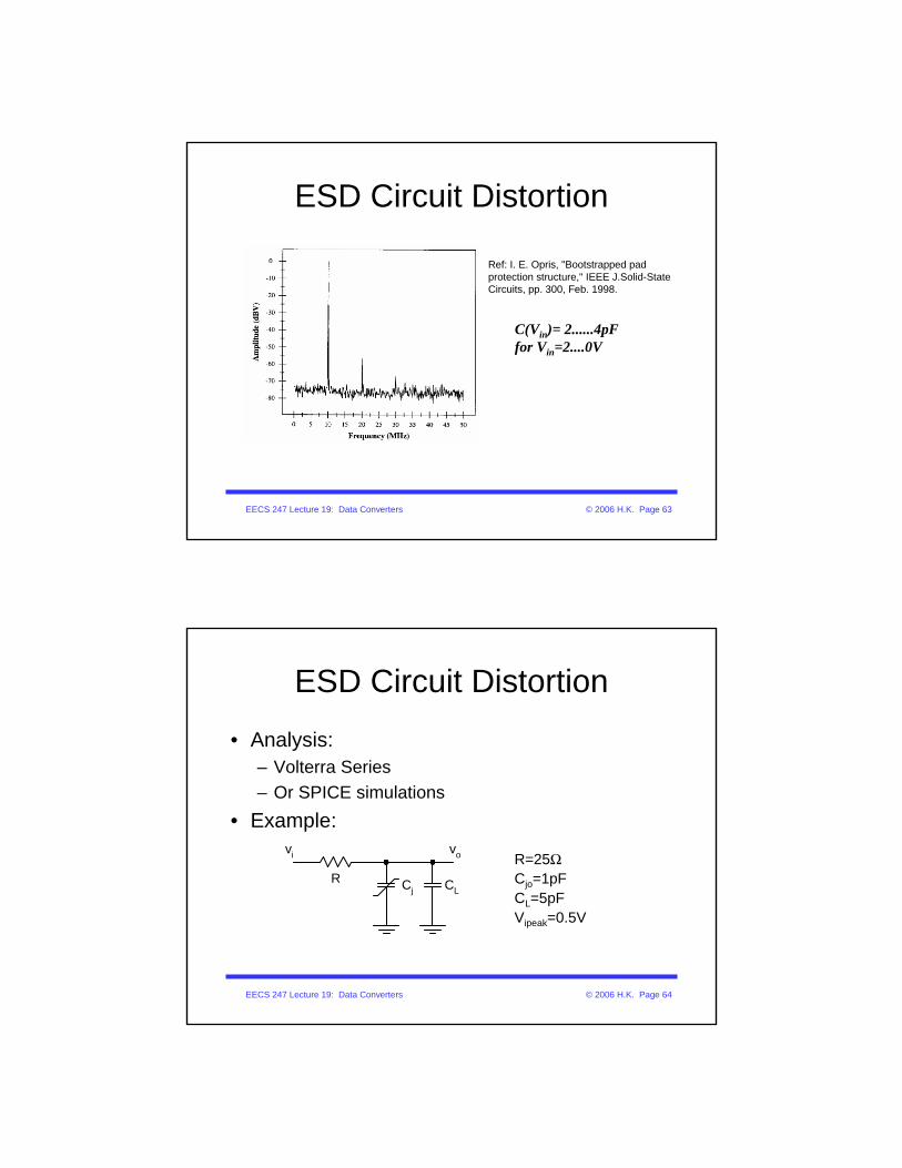
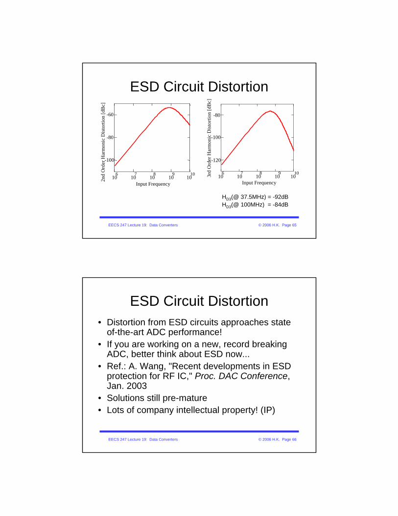
ESD Circuit Distortion
Ref: I. E. Opris, "Bootstrapped pad protection structure," IEEE J.Solid-State Circuits, pp. 300, Feb. 1998.
C(Vin)= 2......4pFfor Vin=2....0V
EECS 247 Lecture 19: Data Converters © 2006 H.K. Page 64
ESD Circuit Distortion
• Analysis: – Volterra Series – Or SPICE simulations
• Example:
R Cj CL
vi vo R=25ΩCjo=1pFCL=5pFVipeak=0.5V
EECS 247 Lecture 19: Data Converters © 2006 H.K. Page 65
ESD Circuit Distortion
HD3(@ 37.5MHz) = -92dBHD3(@ 100MHz) = -84dB
106
107
108
109
1010
-100
-80
-60
2nd
Ord
er H
arm
onic
Dis
torti
on [d
Bc]
Input Frequency
-120
3rd
Ord
er H
arm
onic
Dis
torti
on [d
Bc]
106
107
108
109
1010
Input Frequency
-100
-80
EECS 247 Lecture 19: Data Converters © 2006 H.K. Page 66
ESD Circuit Distortion• Distortion from ESD circuits approaches state
of-the-art ADC performance!• If you are working on a new, record breaking
ADC, better think about ESD now...• Ref.: A. Wang, "Recent developments in ESD
protection for RF IC," Proc. DAC Conference, Jan. 2003
• Solutions still pre-mature• Lots of company intellectual property! (IP)
EECS 247 Lecture 19: Data Converters © 2006 H.K. Page 67
ADC Architectures• Slope Converters• Successive approximation• Flash• Folding• Time-interleaved / parallel converter• Residue type ADCs
– Two-step– Pipeline– Algorithmic– …
• Oversampled ADCs
EECS 247 Lecture 19: Data Converters © 2006 H.K. Page 68
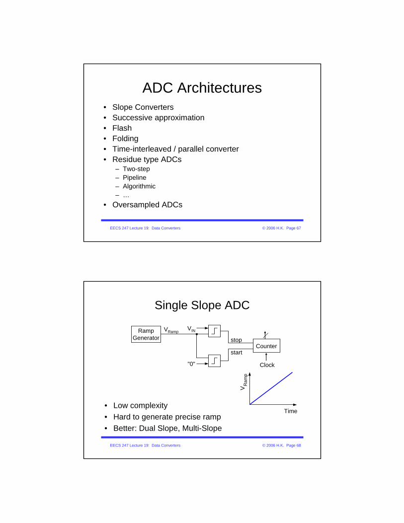
Single Slope ADC
• Low complexity• Hard to generate precise ramp• Better: Dual Slope, Multi-Slope
RampGenerator
Time
VR
amp
VRampVIN
"0"
Counterstop
start
Clock
EECS 247 Lecture 19: Data Converters © 2006 H.K. Page 69
Dual Slope ADC
http://www.maxim-ic.com/appnotes.cfm/appnote_number/1041
• Integrate Vin for fixed time, de-integrate with Vref applied TDe-Int ~ Vin/Vref
• Insensitive to most linear error sources
EECS 247 Lecture 19: Data Converters © 2006 H.K. Page 70
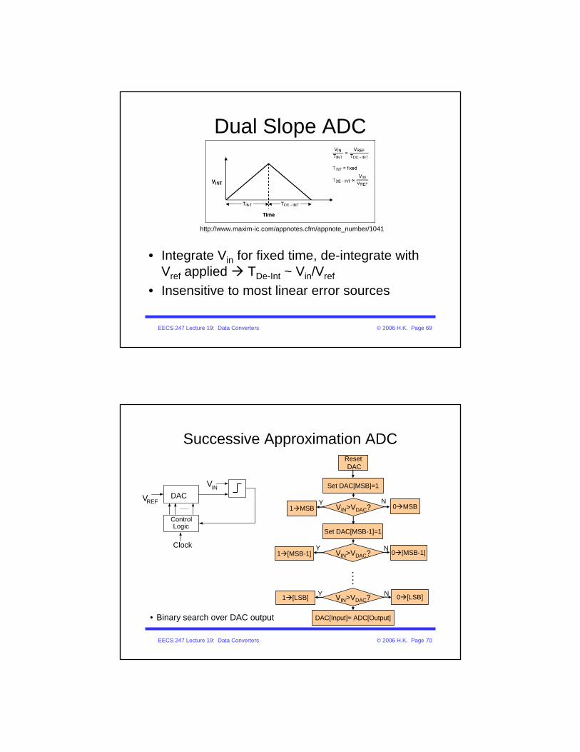
Successive Approximation ADC
• Binary search over DAC output
DACVIN
ControlLogic
Clock
VREF
ResetDAC
Set DAC[MSB]=1
VIN>VDAC?1 MSB 0 MSB
Set DAC[MSB-1]=1
VIN>VDAC?1 [MSB-1] 0 [MSB-1]
....
VIN>VDAC?1 [LSB] 0 [LSB]
DAC[Input]= ADC[Output]
Y
Y
Y
N
N
N

EECS 247 Lecture 19: Data Converters © 2006 H.K. Page 71
Successive Approximation ADC
• High accuracy achievable (16+ Bits) • Moderate speed proportional to B (MHz range)
VDAC/VREF
Time / Clock Ticks
1
1/2
3/45/8
VIN
1/2 3/4 5/8 11/16 21/32 41/64DAC
VIN
ControlLogic
Clock
VREF
Example: 6-bit ADC & VIN=5/8VREF
ADC 101000