Embed Size (px)
Citation preview

Professor Nathan Cheung, U.C. BerkeleyEE143 S06 Lecture#1
1
Instructor : Prof. Nathan Cheung , Cory 513, 642-1615,[email protected]
Lecture Hours and Place: Tu &Th, 8:10-9:30am, 150 GSPPOffice Hours: Tu 11am-1pm, W 1pm-2pm, and by appointment via e-mail
Required Text :1) R.C. Jaeger "Introduction To Microelectronics Fabrication “, 2nd Edition2) EE143 Reader (if you have a F2005 version, no need to buy S2006 version)
Homework: Weekly homework assignments due on Thursdays.
Grading: Midterm1 15%,Midterm2 15%, Final 30% ,Homework 10%, Lab 30%(undergrad and grad will be graded as two separate groups)
**Browse last semester's course content for past lecture notes, homework,and exams. http://www-inst.eecs.berkeley.edu/~ee143/fa05index.html
EE143 General Information
1

Professor Nathan Cheung, U.C. BerkeleyEE143 S06 Lecture#1
2
Lab Sign-up required for ALL students6 Lab Sessions : Tu2-5pm, W 9-12am, W 2-5pm,
Th 2-5pm, Fri 9-12am, Fri 2-5pm
• Sign-up sheets will be posted outside Cory 218 after 10am (1/17, Tue) .You have to sign up personally at Cory 218 before 5pm (1/19,Thur) even you are enrolled by Telebear. If you do not do so, your name will be removed from the class list
• Final lab assignment will be posted outside Cory 218 and on class webpage on 1/20 (Friday).
• Assignment priority : (1) Telebear enrolled, (2) Telebear waitlist , (3) No Telebear enrollment. Order of sign-up not important.
• NO Lab Meeting the week of 1/16

Professor Nathan Cheung, U.C. BerkeleyEE143 S06 Lecture#1
3Week of 1/26
Mandatory Lab attendance required
•You will have lab orientation and have to pass a safety quiz before you are officially enrolled in this course.
•You should show up at the lab session you are assigned. In case of class conflict, you can show up at other lab sessions only for this week. We can only accommodate a maximum of 12 students per session due to safety issues.

Professor Nathan Cheung, U.C. BerkeleyEE143 S06 Lecture#1
4Lectures, HW, Lab Info, and News (check regularly)http://www-inst.eecs.berkeley.edu/~ee143/
Device Physics/ Process Visualization – Highly recommended(Change the device parameters and watch the resultant space charge, energy bands , I-V , C-V etc)http://jas.eng.buffalo.edu/MEMS operation (Good collection of photos and movies)http://mems.sandia.gov/scripts/index.aspSIA Roadmap (Trend and Challenge)http://public.itrs.net/EE Basics (E40 course material)http://www-inst.eecs.berkeley.edu/~ee40/Trends and forecastwww.icknowledge/com
Other Websites for EE143 Overview
4
Professor Nathan Cheung, U.C. BerkeleyEE143 S06 Lecture#1
5What is EE143 all about?
• Microfabrication Principlesfor IC and MEMS
• Hands-on Fabrication and Testing of IC and MEMSDevices
5
Professor Nathan Cheung, U.C. BerkeleyEE143 S06 Lecture#1
6
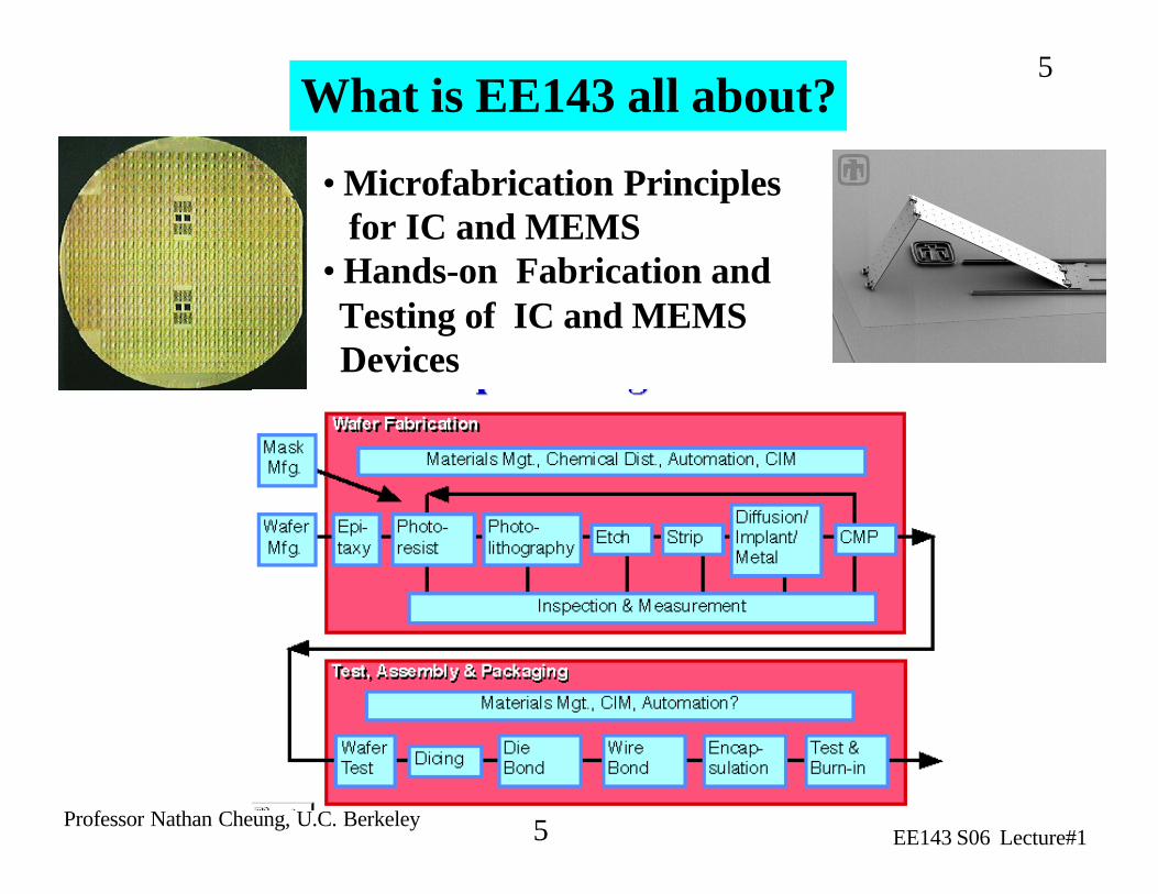
Principle of Monolithic Process Integration
* A sequence of Additive and Subtractivesteps with lateral patterning
ProcessingSteps
Example: CMOS Integrated Circuit
Si wafer

Professor Nathan Cheung, U.C. BerkeleyEE143 S06 Lecture#1
7A Process Module has many sub-steps!
Example : Deep UV Photolithography
Sequence:(1)Surface Prime, (2) Coat, (3) Prebake,(4) Expose, (5) Post Exposure bake,(6) Develop, (7) Hard Bake

Professor Nathan Cheung, U.C. BerkeleyEE143 S06 Lecture#1
8
Example : Deep UV Photolithography(continued)

Professor Nathan Cheung, U.C. BerkeleyEE143 S06 Lecture#1
9
Example : Deep UV Photolithography(continued)
*All baking sub-steps are similarbut with different temperature and time

Professor Nathan Cheung, U.C. BerkeleyEE143 S06 Lecture#1
10
EE143ChipFabrication
10

Professor Nathan Cheung, U.C. BerkeleyEE143 S06 Lecture#1
11Photograph of EE143 Wafer
Professor Nathan Cheung, U.C. BerkeleyEE143 S06 Lecture#1
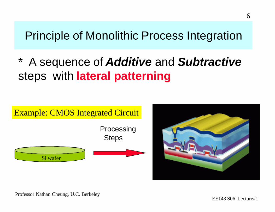
12SEM Micrographs of EE143 Chip

Professor Nathan Cheung, U.C. BerkeleyEE143 S06 Lecture#1
13EE143 Chip Characterization
13
17-stage Ring Oscillator

Professor Nathan Cheung, U.C. BerkeleyEE143 S06 Lecture#1
14
Process Simulation
After resist patterning on nitride/pad oxide
After Local Oxidation After Poly-Si Gate Patterning
* 3D Topography and Dopant Distribution
14
Professor Nathan Cheung, U.C. BerkeleyEE143 S06 Lecture#1
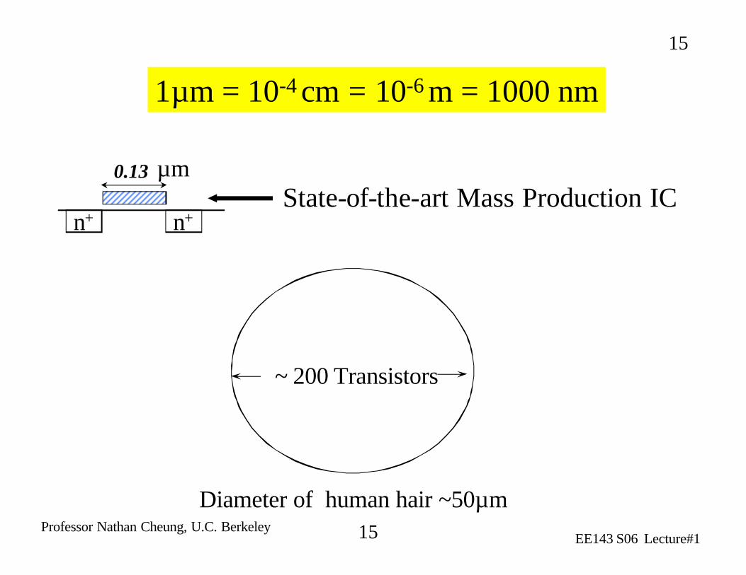
15
0.13
1µm = 10-4 cm = 10-6 m = 1000 nm
~ 200 Transistors
Diameter of human hair ~50µm
n+ n+
µmState-of-the-art Mass Production IC
15

Professor Nathan Cheung, U.C. BerkeleyEE143 S06 Lecture#1
16Advantages of Technology Scaling
Generation:
Intel386™ DXProcessor
Intel486™ DXProcessor
Pentium®
Processor
Pentium® II Processor
1.5µ 1.0µ 0.8µ 0.6µ 0.35µ 0.25µ
• More dies per wafer, lower cost• Higher-speed devices and circuits ( electrical signals travel shorter distances)
16
Professor Nathan Cheung, U.C. BerkeleyEE143 S06 Lecture#1
17

Professor Nathan Cheung, U.C. BerkeleyEE143 S06 Lecture#1
18

Professor Nathan Cheung, U.C. BerkeleyEE143 S06 Lecture#1
19
… we are already producing 1018 transistors per year. Enough to supply every ant on the planet with ten transistors.
Twenty years from now, if the trend continues, there will be more transistors than there will be cells in the total number of human bodies on Earth.
Another Perspective on Moore’s Law

Professor Nathan Cheung, U.C. BerkeleyEE143 S06 Lecture#1
20
20

Professor Nathan Cheung, U.C. BerkeleyEE143 S06 Lecture#1
21
5nm-Gate Nanowire FinFET
2004 Symposium on VLSI Technology, p.196
Professor Nathan Cheung, U.C. BerkeleyEE143 S06 Lecture#1
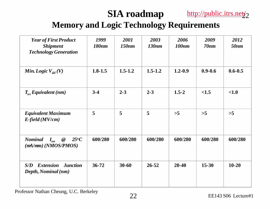
22
Year of First Product Shipment
Technology Generation
1999180nm
2001150nm
2003130nm
2006100nm
200970nm
201250nm
Min. Logic Vdd (V) 1.8-1.5 1.5-1.2 1.5-1.2 1.2-0.9 0.9-0.6 0.6-0.5
Tox Equivalent (nm) 3-4 2-3 2-3 1.5-2 <1.5 <1.0
Equivalent MaximumE-field (MV/cm)
5 5 5 >5 >5 >5
Nominal Ion @ 25oC(µA/µm) (NMOS/PMOS)
600/280 600/280 600/280 600/280 600/280 600/280
S/D Extension JunctionDepth, Nominal (nm)
36-72 30-60 26-52 20-40 15-30 10-20
SIA roadmapMemory and Logic Technology Requirements
http://public.itrs.net/
22

Professor Nathan Cheung, U.C. BerkeleyEE143 S06 Lecture#1
23
Source: Intel Developer Forum 2002
23
Chip Power consumption is a big concern !!!!

Professor Nathan Cheung, U.C. BerkeleyEE143 S06 Lecture#1
24MEMS: Pressure Transducer
Bulk Micromachining
SurfaceMicromachining
Si wafer
Pyrex Glass
Si
24

Professor Nathan Cheung, U.C. BerkeleyEE143 S06 Lecture#1
25
Responsive Drug Delivery Valve
Gear Speed Reduction Unit Movable Mirror
Turbine engine
MEMS Actuators
25

Professor Nathan Cheung, U.C. BerkeleyEE143 S06 Lecture#1
26Commercial MEMS Products
• Optomechanical Displays (TI, 1996)
26
•Acceleratometer( Analog Devices)
Professor Nathan Cheung, U.C. BerkeleyEE143 S06 Lecture#1
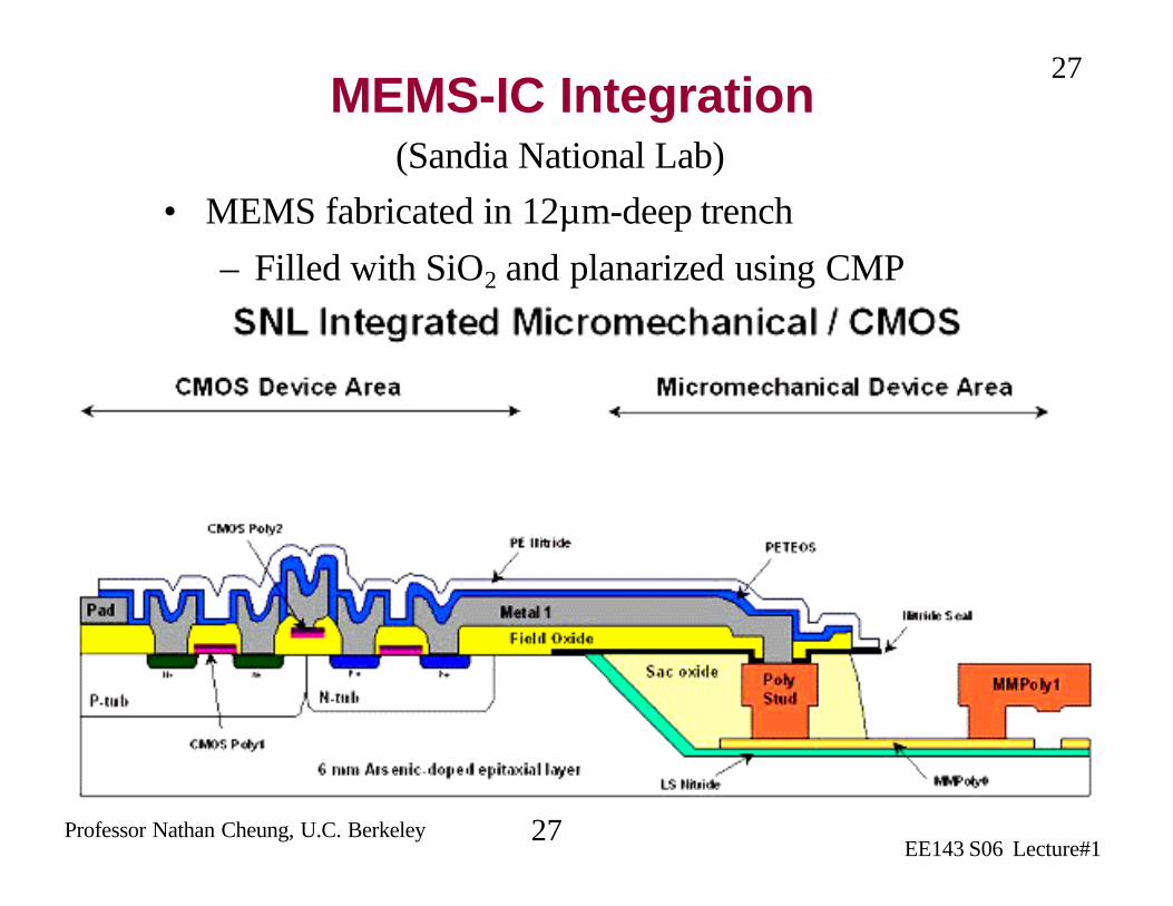
27MEMS-IC Integration
(Sandia National Lab)• MEMS fabricated in 12µm-deep trench
– Filled with SiO2 and planarized using CMP
27

Professor Nathan Cheung, U.C. BerkeleyEE143 S06 Lecture#1
28Silicon-COmpatible OPtoelectronics (SCOOP)
Si-BASED WAVEGUIDES
28

Professor Nathan Cheung, U.C. BerkeleyEE143 S06 Lecture#1
29
‘Snail' neuron grown atop an Infineon Technologies CMOS device that measures the neuron's electrical activity, linking chips and living cells.
Linking Si Technology with Biology
Source: Max Planck Institute

Professor Nathan Cheung, U.C. BerkeleyEE143 S06 Lecture#1
30
http://www.optobionics.com/index.htm
Artificial Silicon Retina™ (ASR)
2mm, 1/1000” thick
30

Professor Nathan Cheung, U.C. BerkeleyEE143 S06 Lecture#1
31Heterogeneous Integration of MicrosystemsProfessor Nathan Cheung, EECS
-
III-V Laser Array
CPU
Micro mirrors
1µm
Micro pump
Micro-fluidic channels
LaserEmitterArrays
LED display
MOS IC
-
Photonics on Si
III-V Laser Array
CPU
Optical Modulator
1µm1µm
Micro pump
200 µm200 µm
Micro-fluidic channels
LaserEmitterArrays
LED display
MOS IC
EncapsulatedPower source
5mm
Green LED
Blue LED5mm5mm5mm
Green LED
Blue LED
BioMEMS Emitters /Filter/Detectors
Encapsulated battery with switch/LED
Si microfluidic channels 200 µm
InGaN LEDs on Si
200 µm200 µm200 µm
InGaN LEDs on Si
Si-Ge high mobilityelectronics
GeOI

Professor Nathan Cheung, U.C. BerkeleyEE143 S06 Lecture#1
32
Extension of Si Technology
Si circuits on plasticSi Laser (Intel)

Professor Nathan Cheung, U.C. BerkeleyEE143 S06 Lecture#1
33
ZnO nanowire array onsapphire substratePeidong Yang, UCB
(i) Co-axial heterostructure nanowire (COHN); (ii) longitudinal heterostructure nanowire (LOHN).
Carbon Sheath around Ge Core Peidong Yang, UCB
Nanoscale Fabrication
Carbon NanotubeMotor A. Zettl, UCB
33