Embed Size (px)
Citation preview

EE136 ProjectSubject:Soft start & E.M.I.
Prof. D ZhouStudent: Dan LeeDate:Dec. 6th,2003
Introduction
• Part1> Soft start
– In converter, the soft start is very important because we do not want the converter to be activated until right voltage and current reached. Also when the converter is activated, we want it to start with narrow pulse width or excessive current could cause
overshoot voltage and saturation on the transformer. • Part2>E.M.I.
– The E.M.I. is serious issue for the electric circuitry in general. And for high switch converter, it require particular attention to take care of E.M.I. Problem because there are multitude of harmonic signals are generated by high frequency square wave.
•
THEORY of CIRCUIT
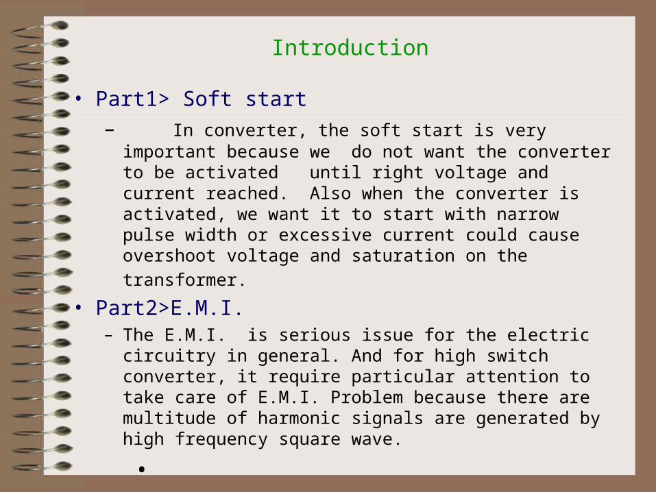
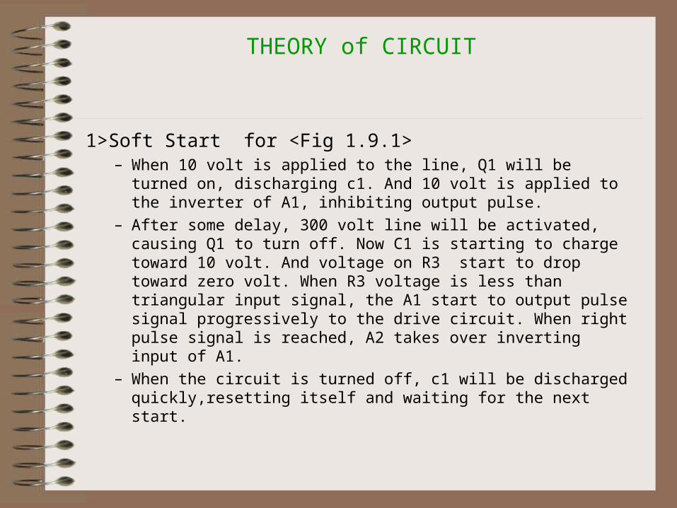
1>Soft Start for <Fig 1.9.1>– When 10 volt is applied to the line, Q1 will be turned on,
discharging c1. And 10 volt is applied to the inverter of A1, inhibiting output pulse.
– After some delay, 300 volt line will be activated, causing Q1 to turn off. Now C1 is starting to charge toward 10 volt. And voltage on R3 start to drop toward zero volt. When R3 voltage is less than triangular input signal, the A1 start to output pulse signal progressively to the drive circuit. When right pulse signal is reached, A2 takes over inverting input of A1.
– When the circuit is turned off, c1 will be discharged quickly,resetting itself and waiting for the next start.
Figure 1.9.1
+
-A1
Q1
D3
C1
R3R2
E1
+
-
A2R4
R5
R1
E3
+
V
VM2
Z200Vdc1
D1
E4
Sine
REF3VDcD2
N1
S1
Ctrl1.VAL
+
V
Sine_1Vac_5Vdc
+
V
Triang5Vdc_1Vpp
300Vdc line
10Vdc line
THEORY of CIRCUIT
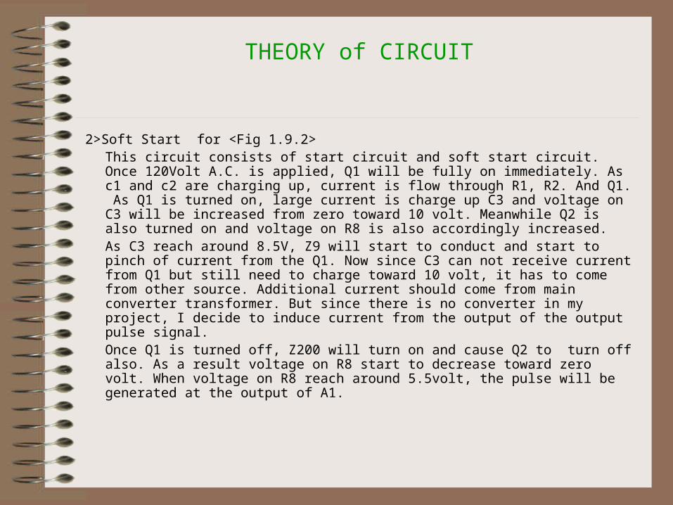
2>Soft Start for <Fig 1.9.2>This circuit consists of start circuit and soft start circuit. Once 120Volt A.C. is applied, Q1 will be fully on immediately. As c1 and c2 are charging up, current is flow through R1, R2. And Q1. As Q1 is turned on, large current is charge up C3 and voltage on C3 will be increased from zero toward 10 volt. Meanwhile Q2 is also turned on and voltage on R8 is also accordingly increased.
As C3 reach around 8.5V, Z9 will start to conduct and start to pinch of current from the Q1. Now since C3 can not receive current from Q1 but still need to charge toward 10 volt, it has to come from other source. Additional current should come from main converter transformer. But since there is no converter in my project, I decide to induce current from the output of the output pulse signal.
Once Q1 is turned off, Z200 will turn on and cause Q2 to turn off also. As a result voltage on R8 start to decrease toward zero volt. When voltage on R8 reach around 5.5volt, the pulse will be generated at the output of A1.
• The delay of start can be controlled by RC constant of C4 and R8. But if these value is too small, they can cause output pulse width to start with maximum width , which can defeat the design purpose.
THEORY of CIRCUIT
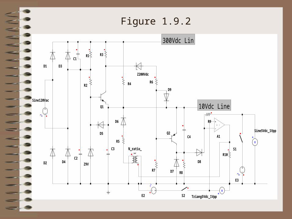
Figure 1.9.2
R1C1
Q2
+
-
A1
Z200Vdc
D1 D3
D2 D4C2
R2
R3
R4
R5
R6
R7R8
R9
C3
C4D5
D6
D7
D8
D9
Z9V
Q1
Sine120Vac
E2
E3
+
V
Sine5Vdc_1Vpp
R10
+
V
Triang5Vdc_1Vpp
S1
S2
TWT
N_ratio_3
300Vdc Line
10Vdc Line
E.M.I.
• Electromagnetic interference is indefatigable in all switch mode power supply. Therefore it is vital to include filter lines.
• There are two kind of E.M.I.; conducted EMI, radiated EMI.
• For this project, I concentrated on conducted EMI.
• There are two kind of conducted EMI; differential mode and common mode.
• Differential mode is the EMI between any two supply or output lines.
• Common mode is EMI between any line to common ground. High frequency switching area is very susceptible for this kind of EMI. These high harmonic frequency with large voltage can connect to ground via heat sink, transformer casing, and etc… , unless the circuit board around it is carefully layed out. Once these EMI slip through ground level, they can propagate through many path, causing headache. Therefore it is better to prevent it than try to suppress it.

E.M.I.
• To design for common mode EMI., we need to comply with FCC’s maximum allowable current. Then we can find value of capacitor. Then we can figure out inductance value for cut off frequency.
• In this project, since maximum current was set to be 0.5mA, C2 was calculated to be 0.01uf for 18khz cut off. Then L1, L2 can easily be calculated to be 2mH, using L1=1 / (C2*[4*Pi*Freq]^2) equation. Although L1,L2 are quite big to attenuate common mode EMI, it will not affect input 60 hz signal much because it was wounded such that magnetic flux will be cancelled out for input low frequency signal.
• . For differential mode, 1uF was chosen for C4 . Then L3, L4 can be calculated easily.

Calculation for filter component
• Using Foster or Caur method isn’t recommended. Because of difficulty of finding Vo/Vin Transfer Function.
• CutOff Freq for C.M. is 18.5Khz.
• C.M. C2= Current / (2*Pi* Freq*Voltage)
• C.M. L1=1 / (C2*[4*Pi*Freq]^2)
• CutOff Freq for D.M. is 16Khz.
• D.M. L3=1/ (C4*[4*Pi*Freq]^2)
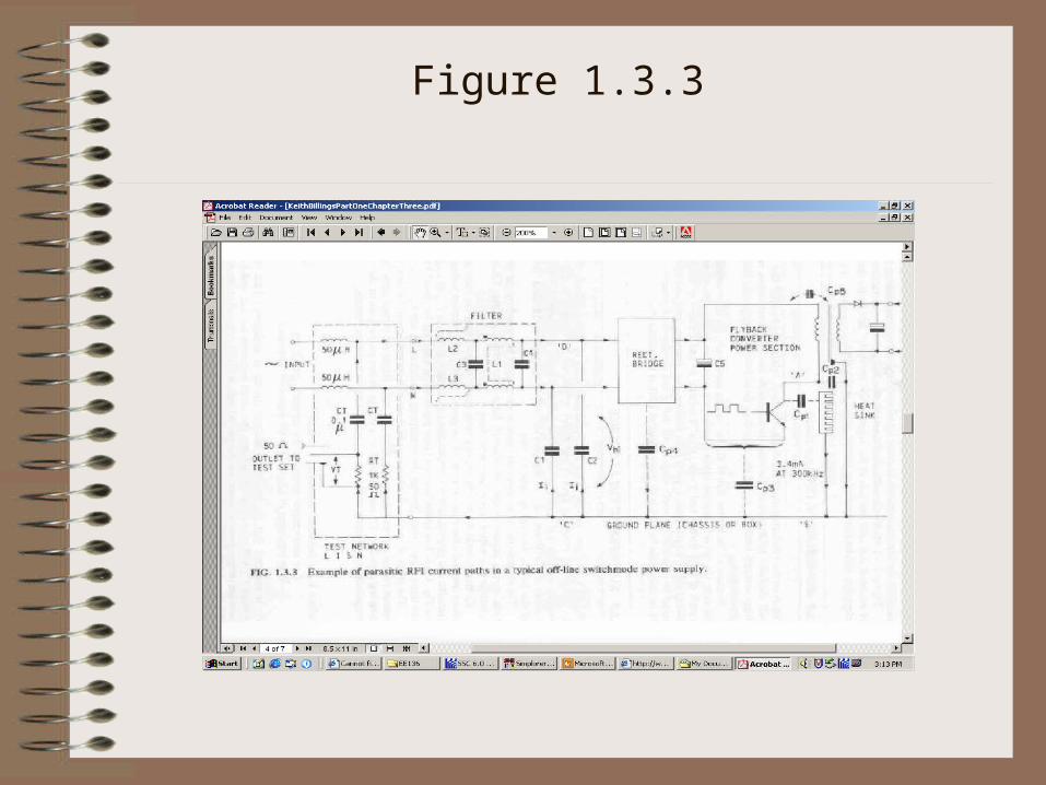
Figure 1.3.3
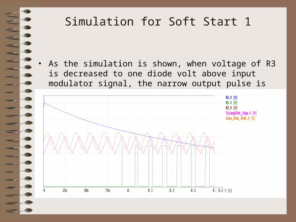
Simulation for Soft Start 1
• As the simulation is shown, when voltage of R3 is decreased to one diode volt above input modulator signal, the narrow output pulse is started to generated.
R3.V [V] R5.V [V] R2.V [V] Triang5Vdc_1Vpp.V [V] Sine_1Vac_5Vdc.V [V]
t [s] 0 0.2125m 50m 75m 0.1 0.13 0.15 0.18 0.2
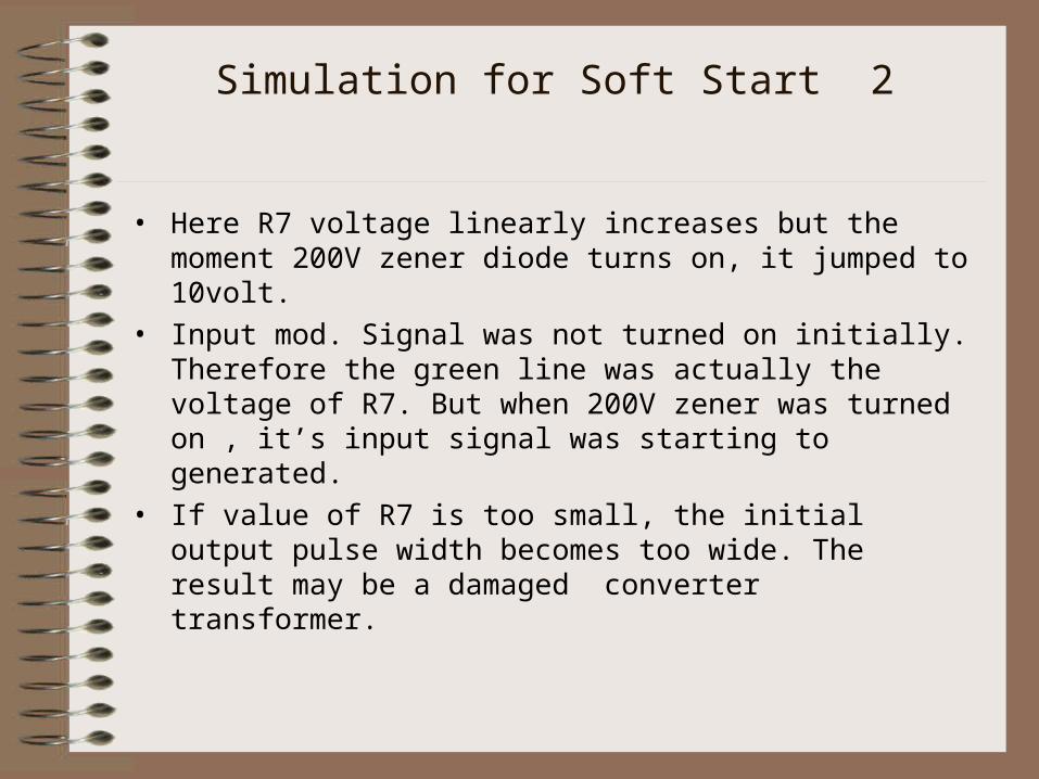
Simulation for Soft Start 2
• Here R7 voltage linearly increases but the moment 200V zener diode turns on, it jumped to 10volt.
• Input mod. Signal was not turned on initially. Therefore the green line was actually the voltage of R7. But when 200V zener was turned on , it’s input signal was starting to generated.
• If value of R7 is too small, the initial output pulse width becomes too wide. The result may be a damaged converter transformer.

Simulation for Soft Start
R10.V [V] R8.V [V] Sine5Vdc_1Vpp.V [V] Triang5Vdc_1Vpp.V [V] R7.V [V]
t [s]
12
-2
0
2
4
6
8
10
0 0.3250m 0.1 0.15 0.2 0.25 0.3
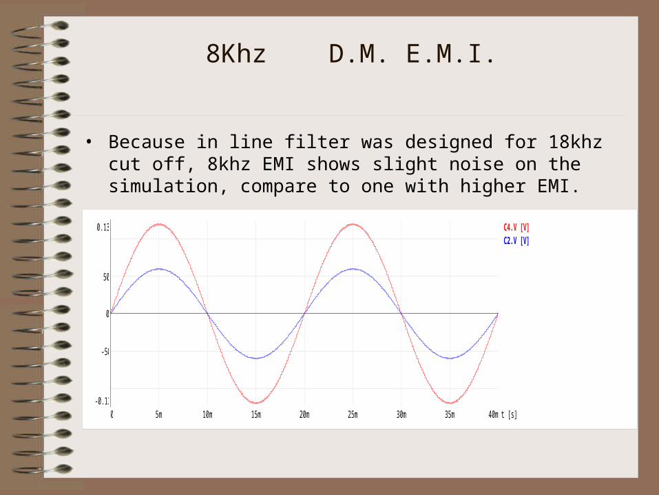
8Khz D.M. E.M.I.
• Because in line filter was designed for 18khz cut off, 8khz EMI shows slight noise on the simulation, compare to one with higher EMI.
C4.V [V] C2.V [V]
t [s]
0.13k
-0.13k
0
-50
50
0 40m5m 10m 15m 20m 25m 30m 35m
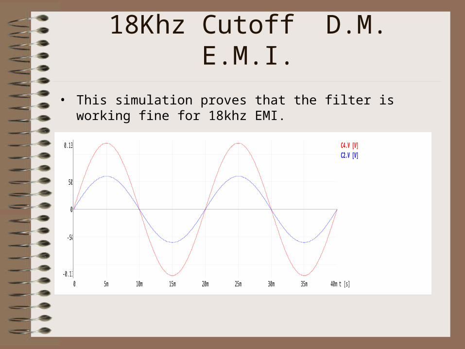
18Khz Cutoff D.M. E.M.I.
• This simulation proves that the filter is working fine for 18khz EMI.
C4.V [V] C2.V [V]
t [s]
0.13k
-0.13k
0
-50
50
0 40m5m 10m 15m 20m 25m 30m 35m

18Khz D.M. E.M.I. W/O L. Filters
• Without proper inductor filter, 18khz EMI generates considerable noise.
C4.V [V] C2.V [V]
t [s]
0.15k
-0.15k
0
-0.1k
-50
50
0.1k
0 20m2m 4m 6m 8m 10m 12m 14m 16m 18m

1.8Mhz Cutoff D.M. E.M.I.
• This filter circuit still holding nicely for 1.8Mhz EMI.
C4.V [V] C2.V [V]
t [s]
0.13k
-0.13k
0
-50
50
0 40m5m 10m 15m 20m 25m 30m 35m
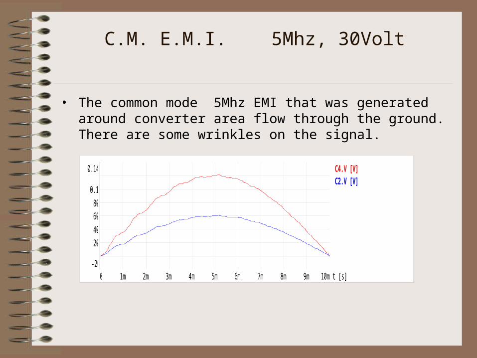
C.M. E.M.I. 5Mhz, 30Volt
• The common mode 5Mhz EMI that was generated around converter area flow through the ground. There are some wrinkles on the signal.
C4.V [V] C2.V [V]
t [s]
0.14k
-20
20
40
6080
0.1k
0 10m1m 2m 3m 4m 5m 6m 7m 8m 9m
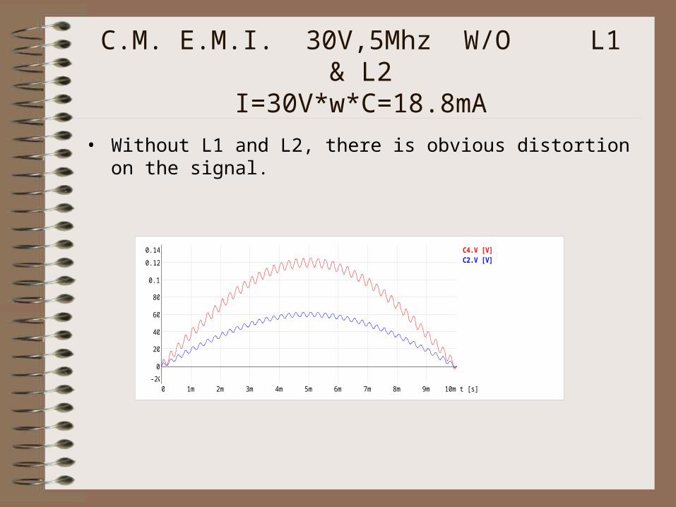
C.M. E.M.I. 30V,5Mhz W/O L1 & L2I=30V*w*C=18.8mA
• Without L1 and L2, there is obvious distortion on the signal.
C4.V [V] C2.V [V]
t [s]
0.14k
-20
0
20
40
60
80
0.1k
0.12k
0 10m1m 2m 3m 4m 5m 6m 7m 8m 9m
Conclusion