Embed Size (px)
Citation preview

EE105 Fall 2011 Lecture 5, Slide 1 Prof. Salahuddin, UC Berkeley
Lecture 5
OUTLINE• PN Junction Diodes
– I/V– Capacitance– Reverse Breakdown– Large and Small signal modelsReading: Chapter 2.2-2.3,3.2-3.4

EE105 Fall 2011 Lecture 5, Slide 2 Prof. Salahuddin, UC Berkeley
Recap: Law of the Junction
0 a-b
Law of the junction:
TD VV �i enapan /2)()(

EE105 Fall 2011 Lecture 5, Slide 3 Prof. Salahuddin, UC Berkeley
Recap: Minority Carrier Concentrations at the Edges of the Depletion Region
n
TDLx
A
VVi
p
ppp
eN
enxn
xnnxn
//2
0
1)(
)()(
x'
Notation:Ln electron diffusion length (cm)
nTD LxVV
nA
inpndiffn ee
LN
nqD
xd
dnqDJ //
2
, 1
0x=a
-b ;x‘=0
EE105 Fall 2011 Lecture 5, Slide 4 Prof. Salahuddin, UC Berkeley
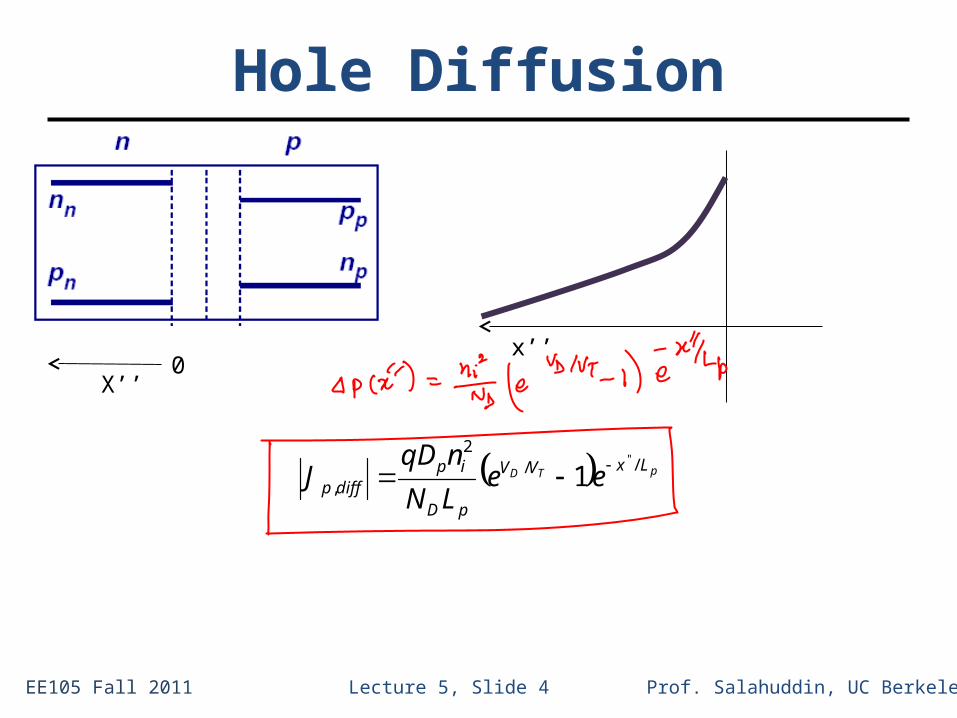
Hole Diffusion
X’’0
pTDLxVV
pD
ipdiffp ee
LN
nqDJ //
2
,
''
1
x’’

EE105 Fall 2011 Lecture 5, Slide 5 Prof. Salahuddin, UC Berkeley
Distribution of Diffusion Current
x0 a-b
nTD LxVV
nA
indiffn ee
LN
nqDJ //
2
, 1 pTDLxVV
pD
ipdiffp ee
LN
nqDJ //
2
, 1
•Assume: No Recombination in the depletion region•Known: Total Current is the same everywhere

EE105 Fall 2011 Lecture 5, Slide 6 Prof. Salahuddin, UC Berkeley
Diode Current under Forward Bias• The current flowing across the junction is comprised
of hole diffusion and electron diffusion components:
0,0,0,0,
xdiffnxdiffpxdriftnxdriftptot JJJJJ
x0 a-b
nTD LxVV
nA
indiffn ee
LN
nqDJ //
2
, 1 pTDLxVV
pD
ipdiffp ee
LN
nqDJ //
2
, 1
J_total

EE105 Fall 2011 Lecture 5, Slide 7 Prof. Salahuddin, UC Berkeley
I-V Characteristic of a PN Junction• Current increases exponentially with applied forward
bias voltage, and “saturates” at a relatively small negative current level for reverse bias voltages.
pD
p
nA
niSS
VVSD
LN
D
LN
DAqnAJI
eII TD
2
/ 1
“Ideal diode” equation:
EE105 Fall 2011 Lecture 5, Slide 8 Prof. Salahuddin, UC Berkeley
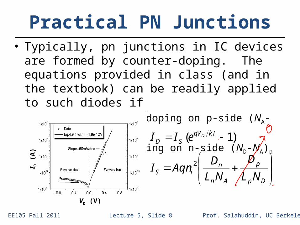
Practical PN Junctions• Typically, pn junctions in IC devices are formed by
counter-doping. The equations provided in class (and in the textbook) can be readily applied to such diodes if– NA net acceptor doping on p-side (NA-ND)p-side
– ND net donor doping on n-side (ND-NA)n-side
)1( kTVqSD
DeII
Dp
p
An
niS NL
D
NL
DAqnI 2
VD (V)
I D (A
)

EE105 Fall 2011 Lecture 5, Slide 9 Prof. Salahuddin, UC Berkeley
How to make sure that current flow in a forward-biased p-n junction diode is mainly due to electrons?

EE105 Fall 2011 Lecture 5, Slide 10 Prof. Salahuddin, UC Berkeley
Diode Saturation Current IS
• IS can vary by orders of magnitude, depending on the diode area, semiconductor material, and net dopant concentrations.– typical range of values for Si PN diodes: 10-14 to 10-17 A/m2
• In an asymmetrically doped PN junction, the term associated with the more heavily doped side is negligible:
– If the P side is much more heavily doped,
– If the N side is much more heavily doped,
Dp
p
An
niS NL
D
NL
DAqnI 2
Dp
piS NL
DAqnI 2
An
niS NL
DAqnI 2

EE105 Fall 2011 Lecture 5, Slide 11 Prof. Salahuddin, UC Berkeley
Depletion Width at Equilibrium
on the P side: xaqN
Esi
A
(see slide 3 in lecture 4)(x)
x-qNA
qND
a
-b
V(x)
xa-b
V0
0
on the N side: bxqN
Esi
D
--(1)
--(2)
DA bNaN --(3)
Let us set the reference point at x=aThen V(a)=0
V(-b)=V0; Built in potential

EE105 Fall 2011 Lecture 5, Slide 12 Prof. Salahuddin, UC Berkeley
Depletion Width at Equilibrium xa
qNE
si
A V(x)
xa-b
V0
0
bxqN
Esi
D
--(1)
--(2)
DA bNaN --(3)
V(a)=0 V(-b)=V0; Built in potential

EE105 Fall 2011 Lecture 5, Slide 13 Prof. Salahuddin, UC Berkeley
Depletion Width at Equilibrium V(x)
xa-b
V0
0

EE105 Fall 2011 Lecture 5, Slide 14 Prof. Salahuddin, UC Berkeley
Depletion Width at biased conditionsV(x)
xa-b
V0
0

EE105 Fall 2011 Lecture 5, Slide 15 Prof. Salahuddin, UC Berkeley
PN Junction Depletion Capacitance• A reverse-biased PN junction can be viewed as a
capacitor, for incremental changes in applied voltage.
dep
sij W
C
si 10-12 F/cm is the permittivity of silicon

EE105 Fall 2011 Lecture 5, Slide 16 Prof. Salahuddin, UC Berkeley
Voltage-Dependent Capacitance• The depletion width (Wdep) and hence the junction
capacitance (Cj) varies with VR.
VD
EE105 Fall 2011 Lecture 5, Slide 17 Prof. Salahuddin, UC Berkeley
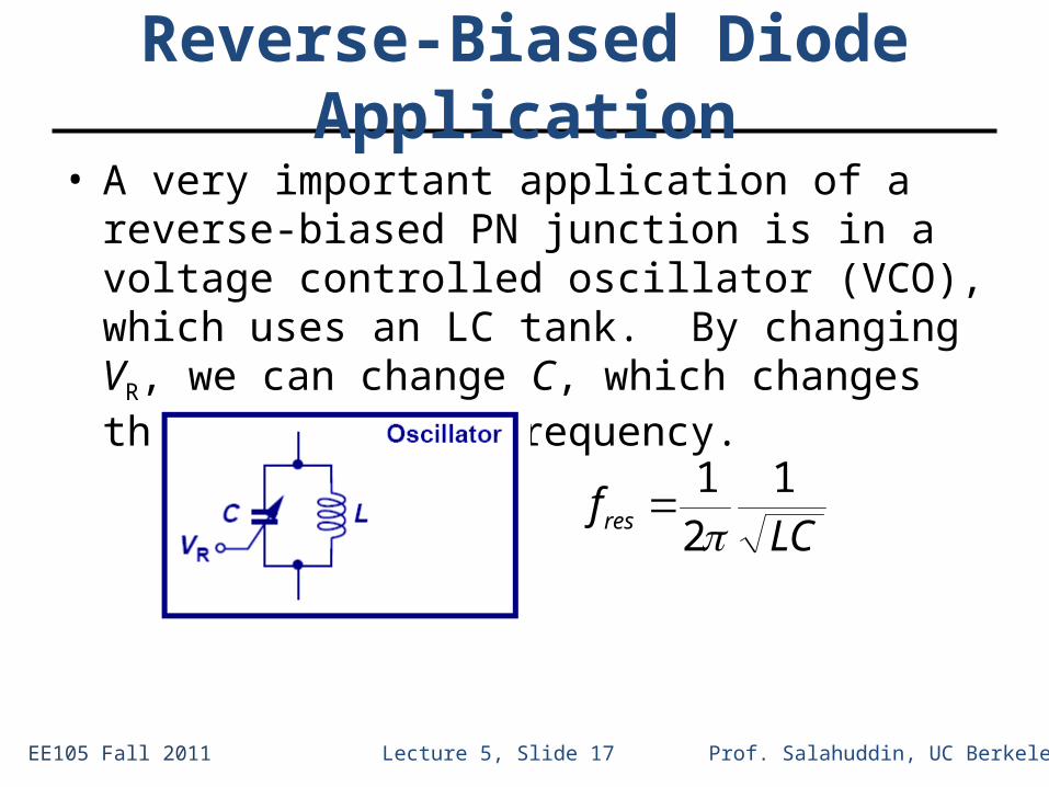
Reverse-Biased Diode Application• A very important application of a reverse-biased PN
junction is in a voltage controlled oscillator (VCO), which uses an LC tank. By changing VR, we can change C, which changes the oscillation frequency.
LCfres
121

EE105 Fall 2011 Lecture 5, Slide 18 Prof. Salahuddin, UC Berkeley
Forward Bias Diffusion capacitance
x’’
At small forward bias, putting a small ac signal changes the concentration of diffused minority carriers and therefore gives a capacitance. This is called a diffusion capacitance