Embed Size (px)
Citation preview

EE105 Fall 2007 Lecture 27, Slide 1 Prof. Liu, UC Berkeley
Lecture 27ANNOUNCEMENTS
• Regular office hours will end on Monday 12/10• Special office hours will be posted on the EE105 website
• Final Exam Review Session: Friday 12/14, 3PM, HP Auditorium– Video will be posted online by Monday 12/17
• Final Exam:– Thursday 12/20, 12:30PM-3:30PM, 277 Cory– Closed book; 6 pages of notes only– Comprehensive in coverage:
• Material of MT#1 and MT#2, plus MOSFET amplifiers, MOSFET current sources, BJT and MOSFET differential amplifiers, feedback.
• Qualitative questions on state-of-the-art device technology

EE105 Fall 2007 Lecture 27, Slide 2 Prof. Liu, UC Berkeley
Outline
• IC technology advancementQ: How did we get here?
• Modern BJT technologyQ: What is an HBT?
• Modern MOSFET technologyQ: What are the challenges (and potential solutions)
for continued MOSFET scaling?

EE105 Fall 2007 Lecture 27, Slide 3 Prof. Liu, UC Berkeley
The IC Market• The semiconductor industry is approaching $300B/yr in sales
Transportation
8%
Consumer Electronics16%
Communications24%
Computers42%
Industrial8%
Military2%
Courtesy of Dr. Bill Flounders, UC Berkeley Microlab
EE105 Fall 2007 Lecture 27, Slide 4 Prof. Liu, UC Berkeley
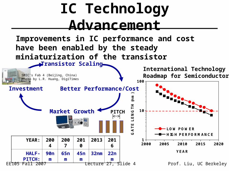
IC Technology AdvancementImprovements in IC performance and cost have been enabled by the steady miniaturization of the transistor
Better Performance/Cost
Market Growth
2000 2005 2010 2015 20201
10
100
GA
TE
LE
NG
TH
(n
m)
YEAR
LOW POWER HIGH PERFORMANCE
International Technology Roadmap for Semiconductors
Transistor Scaling
Investment
SMIC’s Fab 4 (Beijing, China)Photo by L.R. Huang, DigiTimes
PITCH
YEAR: 2004 2007 2010 2013 2016
HALF-PITCH: 90nm 65nm 45nm 32nm 22nm

EE105 Fall 2007 Lecture 27, Slide 5 Prof. Liu, UC Berkeley
The Nanometer Size Scale
Carbon nanotube
MOSFET

EE105 Fall 2007 Lecture 27, Slide 6 Prof. Liu, UC Berkeley
Nanogap DNA Detector
Prof. Luke Lee, BioEngineering Dept.http://www-biopoems.berkeley.edu/
Insulator (
Polysilicon
Insulator (Si3N4) Insulator (Insulator (Si3N4)
Poly-Si
Double-stranded DNA
Poly-Si
Single-stranded DNA
Poly-SiPoly-Si

EE105 Fall 2007 Lecture 27, Slide 7 Prof. Liu, UC Berkeley
• Goal: Mass fabrication (i.e. simultaneous fabrication) of many IC “chips” on each wafer, each containing millions or billions of transistors
• Approach: Form thin films of semiconductors, metals, and insulators over an entire wafer, and pattern each layer with a process much like printing (lithography).
IC Fabrication
Planar processing consists of a sequence of additive and subtractive steps with lateral patterning
oxidationdeposition
ion implantation
etching lithography

EE105 Fall 2007 Lecture 27, Slide 8 Prof. Liu, UC Berkeley
• DEPOSITION of a thin film
• LITHOGRAPHY– Coat with a protective layer– Selectively expose the protective layer– Develop the protective layer
• ETCH to selectively remove the thin film
• Strip (etch) the protective layer
Planar Processing(patented by Fairchild Semiconductor in 1959: J. A. Hoerni, US Patent 3,064,167)
Courtesy of Dr. Bill Flounders, UC Berkeley Microlab

EE105 Fall 2007 Lecture 27, Slide 9 Prof. Liu, UC Berkeley
Deposition/growth
Etch
Epitaxy
Anneal
CMP
Ion Implantation
Test
CD SEMMetrology
DefectDetection
Lithography
Mask Pattern Generation
Bare SiliconWafer
ProcessedWafer
Overview of IC Process Steps
Courtesy of Dr. Bill Flounders, UC Berkeley Microlab

EE105 Fall 2007 Lecture 27, Slide 10 Prof. Liu, UC Berkeley
Features:• Narrow base • n+ poly-Si emitter• Self-aligned p+ poly-Si base contacts• Lightly-doped collector• Heavily-doped epitaxial subcollector• Shallow trenches and deep trenches filled with SiO2 for electrical isolation
B E C
p+ p+ P base
N collector
N+ subcollector
P substrate
N+ polySi
N+
Deeptrench
Deep trench
Shallowtrench
P+polySiP+polySi
Modern BJT Structure

EE105 Fall 2007 Lecture 27, Slide 11 Prof. Liu, UC Berkeley
BJT Performance Parameters• Common emitter current gain, :
• The cutoff frequency, fT, is the frequency at whichfalls to 1.It is correlated with the maximum frequency of oscillation, fmax.
• Intrinsic gain
BBiEE
EEiBB
EE
iEEE
BB
iBBE
B
C
WNnD
WNnD
WN
nDqA
WN
nDqA
I
I2
2
2
2
T
A
C
A
T
Com V
V
I
V
V
Irg
EE105 Fall 2007 Lecture 27, Slide 12 Prof. Liu, UC Berkeley
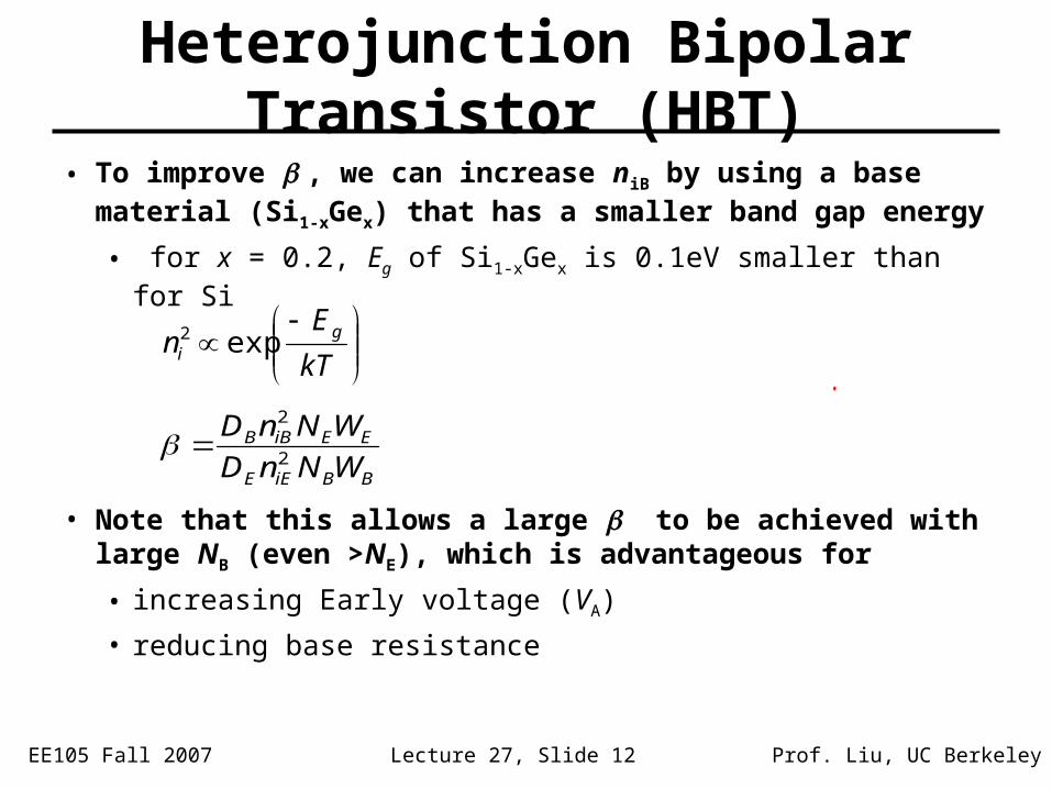
• To improve , we can increase niB by using a base material (Si1-xGex) that has a smaller band gap energy
• for x = 0.2, Eg of Si1-xGex is 0.1eV smaller than for Si
• Note that this allows a large to be achieved with large NB (even >NE), which is advantageous for
• increasing Early voltage (VA)• reducing base resistance
Heterojunction Bipolar Transistor (HBT)
kT
En gi exp2
BBiEE
EEiBB
WNnD
WNnD2
2

EE105 Fall 2007 Lecture 27, Slide 13 Prof. Liu, UC Berkeley
Modern MOSFET Structures(Intel Penryn, from www.semiconductor.com)
• 45nm CMOS technology features:– High-permittivity gate dielectric and metal gate electrodes– strained channel regions– shallow trench isolation
N-channel MOSFETs P-channel MOSFETs
EE105 Fall 2007 Lecture 27, Slide 14 Prof. Liu, UC Berkeley
MOSFET Performance Parameters
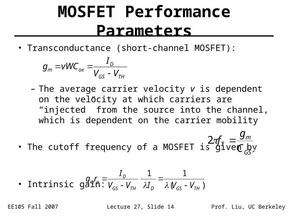
• Transconductance (short-channel MOSFET):
– The average carrier velocity v is dependent on the velocity at which carriers are “injected” from the source into the channel, which is dependent on the carrier mobility
• The cutoff frequency of a MOSFET is given by
• Intrinsic gain:
THGS
Doxm VV
IvWCg
)(
11
THGSDTHGS
Dom VVIVV
Irg
GS
mT C
gf 2

EE105 Fall 2007 Lecture 27, Slide 15 Prof. Liu, UC Berkeley
MOSFET Scaling Challenges• Suppression of short-channel effects
– Gain in ION is incommensurate with Lg scaling
• Variability in performance– Sub-wavelength lithography:
(Costly resolution-enhancement techniques are needed)
– Random variations:• Photoresist line-edge roughness
• Statistical dopant fluctuations
Substrate
Gate
Source Drain
Substrate
Gate
Source Drain
MOSFET:
LeffNsub
Xj
Lg
Tox
Design
Mask
Wafer
250nm250nm 180nm180nm
OPCOPC
90nm and Below90nm and Below
PSM
0°
180°
PSMPSM
0°
180°
0°
180°
OPC0°
180°OPCOPCOPC
0°
180°
photoresist SiO2
Gate
A. Brown et al., IEEE Trans. Nanotechnology, p. 195, 2002
Source Drain

EE105 Fall 2007 Lecture 27, Slide 16 Prof. Liu, UC Berkeley
“VTH Roll-Off”• |VTH| decreases with Lg
– Effect is exacerbated by high values of |VDS|
• Qualitative explanation:– The source & drain p-n junctions assist in depleting the Si underneath
the gate. The smaller the Lg, the greater the percentage of charge balanced by the S/D p-n junctions:
M. Okuno et al., 2005 IEDM p. 52
Large Lg: S D
Small Lg: DS
n+n+
VG
p depletion region
xj

EE105 Fall 2007 Lecture 27, Slide 17 Prof. Liu, UC Berkeley
Why New Transistor Structures?• DIBL must be suppressed to scale down Lg
• Leakage occurs in region far from channel surface Let’s get rid of it!
DrainSource
Gate
Lg
Thin-BodyMOSFET
Buried Oxide
Source Drain
Gate
Substrate
“Silicon-on-Insulator”
(SOI)Wafer

EE105 Fall 2007 Lecture 27, Slide 18 Prof. Liu, UC Berkeley
Thin-Body MOSFETs• Leakage is suppressed by using a thin body (TSi < Lg)
– Channel doping is not needed higher carrier mobility
• Double-gate structure is more scalable (to Lg<10nm)
Ultra-Thin Body (UTB)
Buried Oxide
Substrate
Source Drain
Gate
TSi
Lg
Double-Gate (DG)
Gate
Source Drain
Gate
TSi

EE105 Fall 2007 Lecture 27, Slide 19 Prof. Liu, UC Berkeley
Double-Gate “FinFET”
Planar DG-FET
Gate
Source Drain
Gate
TSi
Fin Width = TSi
Lg
GATE
SOURCE
DRAIN20 nm
10 nmY.-K. Choi et al. (UC Berkeley), IEDMTechnical Digest, pp. 421-424, 2001
15nm Lg FinFET:
Fin Height HFIN = W/2
D. Hisamoto et al. (UC Berkeley), IEDM Technical Digest, pp. 1032-1034, 1998
N. Lindert et al. (UC Berkeley), IEEE Electron Device Letters, pp. 487-489, 2001
FinFET
Source
DrainGate
Lg

EE105 Fall 2007 Lecture 27, Slide 20 Prof. Liu, UC Berkeley
15 nm Lg FinFETs
-1.0 -0.5 0.0 0.5 1.0 1.5 2.010-12
10-10
10-8
10-6
10-4
10-2
10-12
10-10
10-8
10-6
10-4
10-2
N-body=
2x1018cm-3
P+Si0.4
Ge0.6
Gate
NMOSPMOS
Vd=-0.05 V
Vd=-1.0 V
Vd=0.05 V
Vd=1.0 V
Dra
in C
urre
nt, I
d [A
/um
]
Gate Voltage, Vg [V]
-1.5 -1.0 -0.5 0.0 0.5 1.0 1.50
100
200
300
400
500
600
0
100
200
300
400
500
600
Voltage step : 0.2V
|Vg-V
t|=1.2V NMOSPMOS
Dra
in C
urre
nt, I
d[u
A/u
m]
Drain Voltage, Vd [V]
TSi = 10 nm; Tox = 2.1 nm
Y.-K. Choi et al. (UC Berkeley), IEDM Technical Digest, pp. 421-424, 2001
Transfer Characteristics Output Characteristics

EE105 Fall 2007 Lecture 27, Slide 21 Prof. Liu, UC Berkeley
10 nm Lg FinFETsB. Yu et al. (AMD & UC Berkeley), IEDM Technical Digest, pp. 251-254, 2002
220ÅSiO2 cap
Lg=10nm
BOX
NiSi
Poly-Si
Si Fin
Source
DrainGate

EE105 Fall 2007 Lecture 27, Slide 22 Prof. Liu, UC Berkeley
G
S D
Si classical
multi-gateG
S DSi
G
high- gate dielectric
metallic gate
strained Si
Lg (nm): 50 40 30 20 10
MOSFET Scaling Scenario• Advanced structures will enable Si MOSFET scaling to Lg <10 nm
forward body biasing

EE105 Fall 2007 Lecture 27, Slide 23 Prof. Liu, UC Berkeley
The End is Not the Limit !
Information technology pervasive embedded human-centered solving societal-
scale problems
Philips
Innovations in process technology, materials, and device design will sustain the Si revolution
Lower Power,Lower Cost
Market Growth
Technology, Device & CircuitInnovations,
Heterogeneous Integration
Investment
Acknowledgement: Mark Weiser
UbiComp (>1 computers per person)
today
SA
LES
($)/
YR
TIME
PCs (1 person/computer)Mainframes (>1 persons per computer)
Transportation
Healthcare Disaster response
Energy
Environment
Sensatex
Information technology will be pervasive embedded human-centered
for better quality-of-life

EE105 Fall 2007 Lecture 27, Slide 24 Prof. Liu, UC Berkeley
EECS 105 in the Grand Scheme • Example electronic system: cell phone


![Disposition and metabolism of [ c]- levomilnacipran, a ... · 1 hour, 2 hours, 2.5 hours, 3 hours, 3.5 hours, 4 hours, 5 hours, 6 hours, 8 hours, 10 hours, 12 hours, 24 hours, 48](https://img.pdfslide.us/doc/110x75/5f73b26d02e65a52de6394cc/disposition-and-metabolism-of-c-levomilnacipran-a-1-hour-2-hours-25.jpg)


![OS-Unix Command 2019-20 · 1Prof. Maulik Trivedi, CE Department| 3140702–Operating System (2019-20) 1) cal:- Displays a calendar Syntax: - cal [options] [ month ] [year] Description:](https://img.pdfslide.us/doc/110x75/60c93bec6fd5243a97342b38/os-unix-command-2019-20-1prof-maulik-trivedi-ce-department-3140702aoperating.jpg)