Embed Size (px)
Citation preview

EE 434Lecture 2
Basic Concepts

Review from Last Time
• Semiconductor Industry is One of the Largest Sectors in the World Economy and Growing
• All Initiatives Driven by Economic Opportunities and Limitations
• Rapidly Growing Device Count and Rapidly Shrinking Feature Sizes (Moore’s Law?)
• Designers Must Handle Incredible Complexity Yet Work in Large Teams and Make Almost No Mistakes
• Understand the Big Picture and Solve the Right Problem

ITRS Technology Predictions
ITRS 2004 Supply Voltage Predictions
00.5
11.5
22.5
33.5
2000 2005 2010 2015 2020YEAR
Vol
ts Analog
Digital
Review from Last Time

ITRS Technology Predictions
Minimum ASIC Gate Length
0
20
40
60
80
100
120
2000 2005 2010 2015 2020
YEAR
Leng
th in
nm
Review from Last Time

How can complex circuits with a very large number of transistors be efficiently designed
with low probability of error?
• Many designers often work on a single design
• Single error in reasoning, in circuit design, or in implementing circuit on silicon generally results in failure
• Design costs and fabrication costs for test circuits are very high– Design costs for even rather routine circuits often a few million dollars and some
much more– Masks and processing for state of the art processes often between $1M and $2M
• Although much re-use is common on many designs, considerable new circuits that have never been designed or tested are often required
• Time to market critical – missing a deadline by even a week or 2 may kill the market potential

How can complex circuits with a very large number of transistors be efficiently designed
with low probability of error?
• CAD tools and CAD-tool environment critical for success today
• Small number of VLSI CAD toolset vendors• CAD toolset helps the engineer and it is highly
unlikely the CAD tools will replace the design engineer
• Major emphasis in this course on using toolset to support the design process

CAD Environment for Integrated Circuit Design
• Typical Tool Flow– (See Chapter 8 of Text)
• Laboratory Experiments in Course

Analog Flow System Description
Circuit Design (Schematic)
SPICE Simulation
Extraction LVS
DRC Report LVS Output File
Print Circuit Schematic
Layout/DRC
Back-AnnotatedExtraction
Post-Layout SimulationPost-Layout Simulation
Simulation Results
Fabrication
VLSI Design Flow Summary
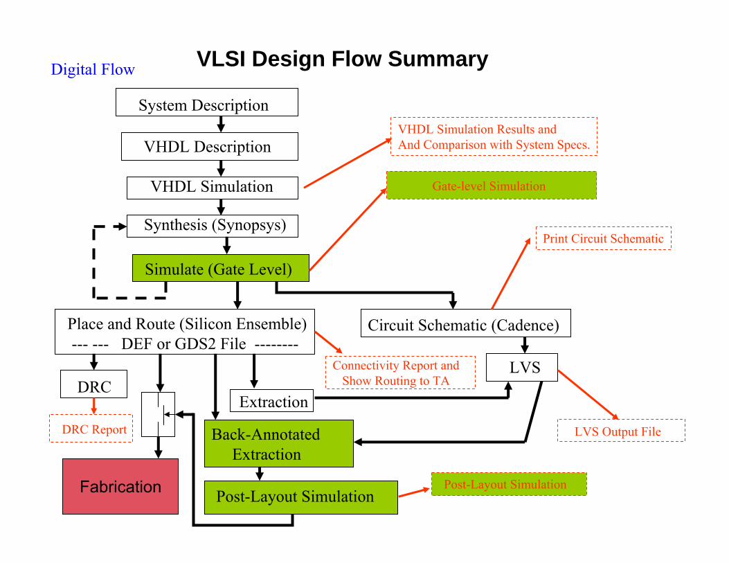
VLSI Design Flow SummaryDigital Flow
System Description
VHDL Description
VHDL Simulation
Synthesis (Synopsys)
Place and Route (Silicon Ensemble)--- --- DEF or GDS2 File --------
Simulate (Gate Level)
Circuit Schematic (Cadence)
DRCExtraction
LVS
VHDL Simulation Results and And Comparison with System Specs.
Gate-level Simulation
Connectivity Report and Show Routing to TA
DRC Report LVS Output File
Print Circuit Schematic
Fabrication
Back-AnnotatedExtraction
Post-Layout SimulationPost-Layout Simulation

VLSI Design Flow Summary
System Description
VHDL Description
VHDL Simulation
Synthesis (Synopsys)
Place and Route (Silicon Ensemble)--- --- DEF or GDS2 File --------
Simulate (Gate Level)
Circuit Schematic (Cadence)
DRCExtraction
LVS
VHDL Simulation Results and And Comparison with System Specs.
Gate-level Simulation
Connectivity Report and Show Routing to TA
DRC Report LVS Output File
Print Circuit Schematic
Back-AnnotatedExtraction
Post-Layout Simulation
Post-Layout Simulation
Mixed Signal Flow (Digital Part)
A B

Mixed-Signal Flow (Analog Part)
System Description
Circuit Design (Schematic)
SPICE Simulation
Extraction LVS
DRC Report LVS Output File
Print Circuit Schematic
C D
Layout/DRC
Back-AnnotatedExtraction
Post-Layout SimulationPost-Layout Simulation
Simulation Results
VLSI Design Flow Summary

A B
Schematic MergeLayout Merge
Extraction
LVS/DRC
Post-Layout Simulation
C D
Show Layout to TA
LVS/DRC Output Files
Simulation Results
VLSI Design Flow SummaryMixed-Signal Flow (Analog-Digital Merger)
Fabrication

Comments
• The Analog Design Flow is often used for small digital blocks or when particular structure or logic styles are used in digital systems
• Variants of these flows are widely used and often personalized by a given company or for specific classes of circuits

Wafer
• 6 inches to 12 inches in diameter• All complete cells ideally identical• flat edge• very large number of die if die size is small die

Feature SizeFeature size is the minimum lateral feature
size that can be reliably manufactured
Often given as either feature size or pitch
Minimum feature size often identical for different features

What is meant by “reliably”
Yield is acceptable if a very large number of these features are made
If P is the probability that a feature is good
n is the number of features on an IC
Y is the yield
nPY =
nYloge
eP =

Example: How reliable must a feature be?
n=5E3Y=0.9
5E30.9log
nYlog ee
eeP == =0.999979
5E30.9log
nYlog ee
eeP == =0.999999999979
But is n=5000 large enough ?
More realistically n=5E9
Extremely high reliability must be achieved in all processing steps to obtain acceptable yields in state of the art processes

Feature Size
• Typically minimum length of a transistor• Often minimum width or spacing of a metal
interconnect (wire)• Point of “bragging” by foundries
– Drawn length and actual length differ• Often specified in terms of pitch
– Pitch approximately equal to twice minimum feature size

Feature Size Evolution
20nm2020
45nm2010
90nm2005
25µMid 70’s
o463 A1010101 === − mnmµ

MOS Transistor
Active
Poly

MOS Transistor
Region of Interest(Channel)
Gate
Source Drain
WL
Drawn Length and Width Shown

MOS Transistor
Gate
Source Drain
WL
Actual Drain and Source at Edges of Channel

MOS Transistor
Gate
Source Drain
Weff Leff
Effective Width and Length Generally Smaller than Drawn Width and Length

Technology Nomenclature
• SSI Small Scale Integration 1-100 • MSI Medium Scale Integration 100-103
• LSI Large Scale Integration 103-105
• VLSI Very Large Scale Integration 105-106
Any design in a process capable of incorporating a large number of devices is generally termed a VLSI design

Device and Die Costs
( )( )
112.525.04
2
2
EinAA
ntrans
wafertrans ==≅
µπ
Consider the high-volume incremental costs of manufacturing integrated circuits
Example: Assume an 8” wafer in a 0.25µ process costs $800
Determine the number of minimum-sized transistors that can be fabricated on this wafer and the cost per transistor. Neglect spacing and interconnect.
Solution:
94.15$112.5
800$−=== E
EnC
Ctrans
wafertrans
Note: the device count may be decreased by a factor of 10 or more ifInterconnect and spacing is included but even with this decrease, the cost per transistor is still very low!

Device and Die Costs2/5.2$ cmC areaunitper ≅
Actual integrated op amp will be dramatically less if bonding pads are not needed
Example: If the die area of the 741 op amp is 1.8mm2, determine the cost of the silicon needed to fabricate this op amp
( ) 05$.8.1/5.2$ 22741 ≅•= mmcmC

End of Lecture 2


![EE 330 Lecture 42 - Iowa State Universityclass.ece.iastate.edu/ee330/lectures/EE 330 Lect 42 Fall 2016.pdf · EE 330 Lecture 42 Digital Circuits • Elmore Delay ... Elmore delay[1]](https://img.pdfslide.us/doc/110x75/5b57fe847f8b9a4e1b8b664d/ee-330-lecture-42-iowa-state-330-lect-42-fall-2016pdf-ee-330-lecture-42-digital.jpg)