Embed Size (px)
Citation preview
ECE 663
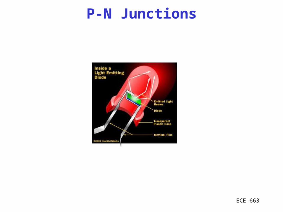
P-N Junctions
ECE 663
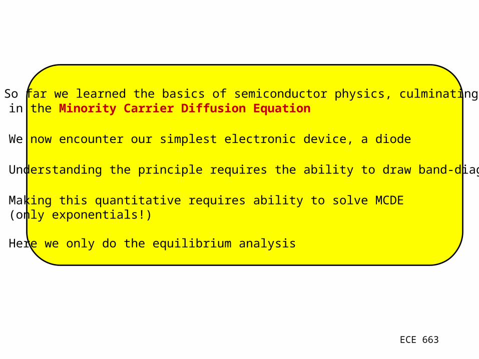
• So far we learned the basics of semiconductor physics, culminating in the Minority Carrier Diffusion Equation
• We now encounter our simplest electronic device, a diode
• Understanding the principle requires the ability to draw band-diagrams
• Making this quantitative requires ability to solve MCDE (only exponentials!)
• Here we only do the equilibrium analysis
ECE 663
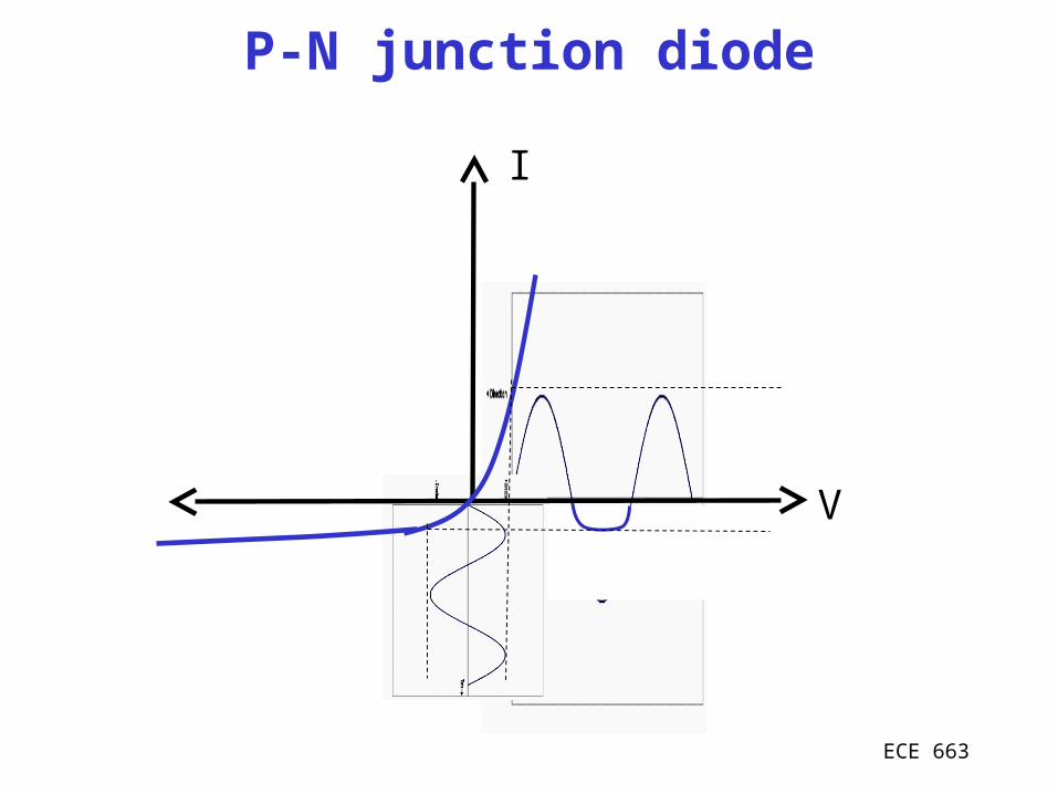
P-N junction diode
V
I

ECE 663
P-N junction diode
V
I
I = I0(eqV/kT-1)
pn v
Ip0 = q(ni2/ND) (Lp/p)

ECE 663
P-N Junctions - Equilibrium
<= P-type, low EF
- = fixed ionized acceptors
+ = mobile holes, p
<= N-type, high EF
+ = fixed ionized donors
- = mobile electrons, n
What happens when these bandstructures collide?
• Fermi energy must be constant at equilibrium, so bands must bend near interface
• Far from the interface, bandstructures must revert
ECE 663
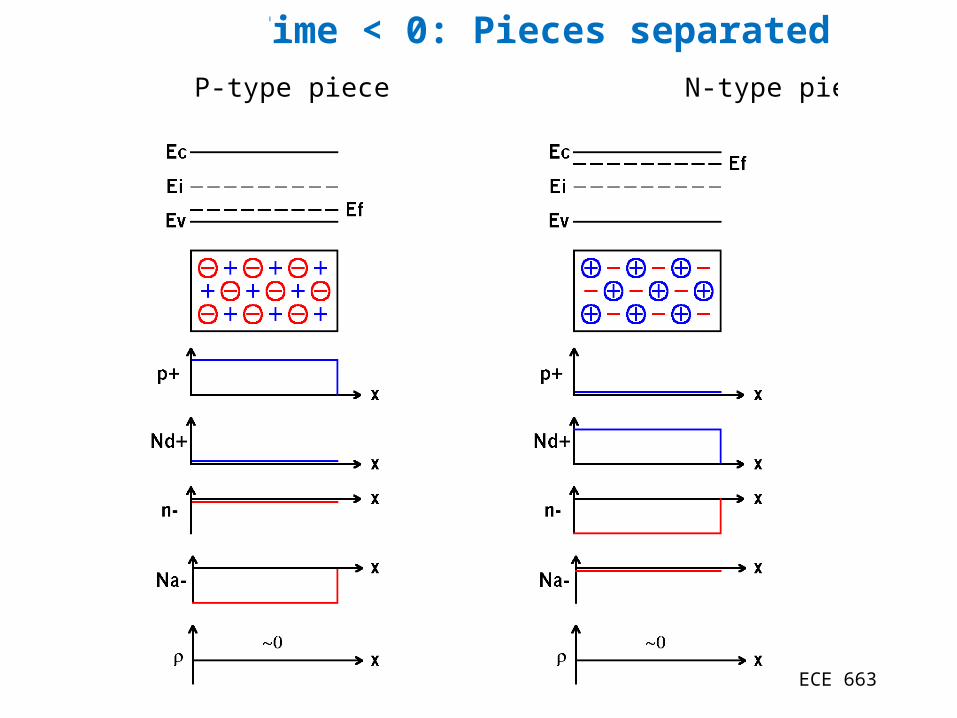
Time < 0
P-type piece N-type piece
Time < 0: Pieces separated
ECE 663
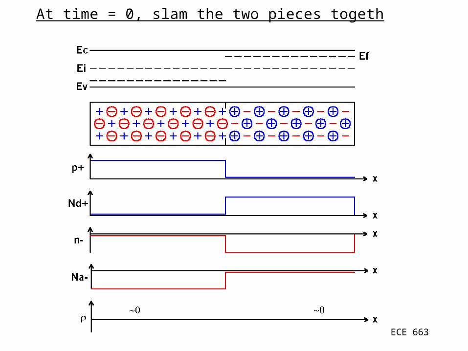
At time = 0, slam the two pieces together
ECE 663
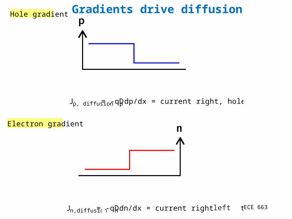
Hole gradient
Jp, diffusion = -qDp dp/dx = current right, holes right
Electron gradient
Jn,diffusion = -qDn dn/dx = current right, electrons right
Gradients drive diffusion
left
ECE 663
Gradients drive diffusion
ECE 663
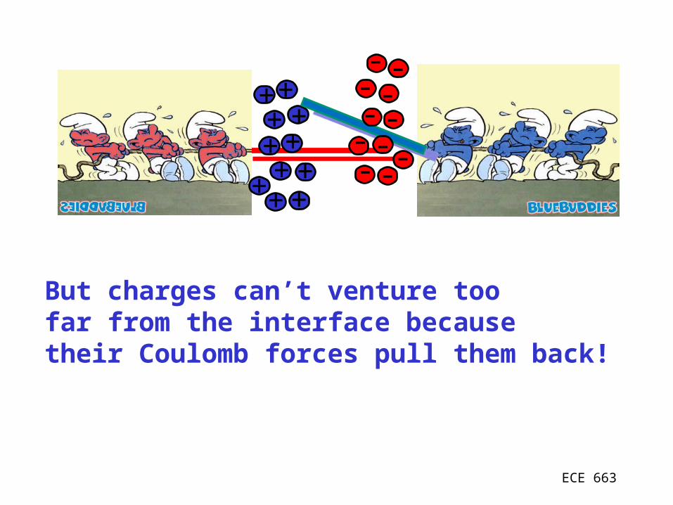
But charges can’t venture toofar from the interface becausetheir Coulomb forces pull them back!
++- -
++++
- -- -
- -- -
-+++++
ECE 663
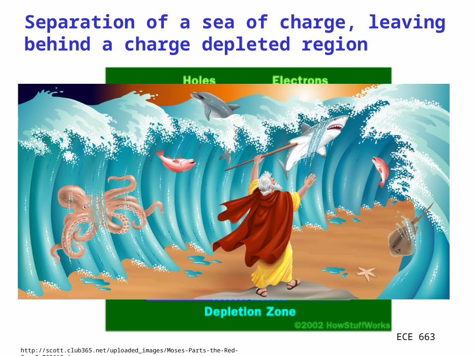
Separation of a sea of charge, leavingbehind a charge depleted region
http://scott.club365.net/uploaded_images/Moses-Parts-the-Red-Sea-2-782619.jpg
ECE 663
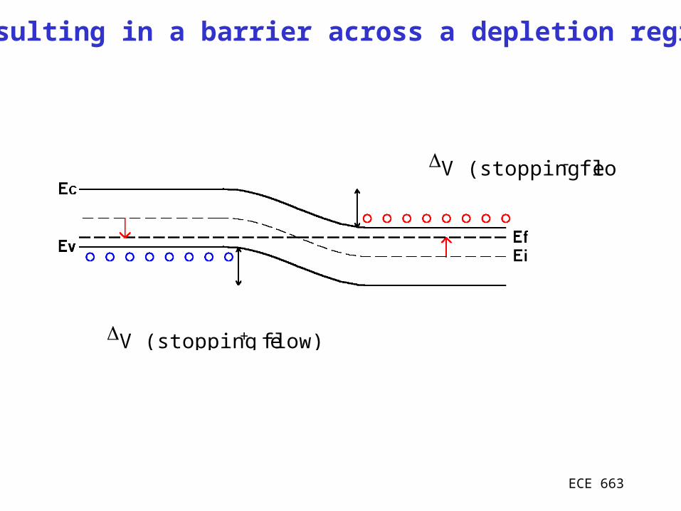
V (stopping e - flow)
V (stopping e+ flow)
Resulting in a barrier across a depletion region
ECE 663E
E
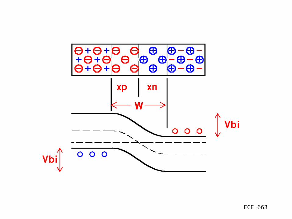
Depletion Region
ECE 663
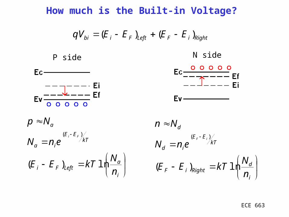
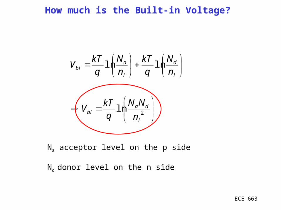
How much is the Built-in Voltage?
RightiFLeftFibi EEEEqV )()(
P side N side
i
aLeftFi
kTEE
ia
a
nN
kTEE
enN
NpFi
ln)(
)(
i
dRightiF
kTEE
id
d
nN
kTEE
enN
NniF
ln)(
)(
ECE 663
2ln
lnln
i
dabi
i
d
i
abi
n
NNq
kTV
nN
qkT
nN
qkT
V
Na acceptor level on the p side
Nd donor level on the n side
How much is the Built-in Voltage?
ECE 663
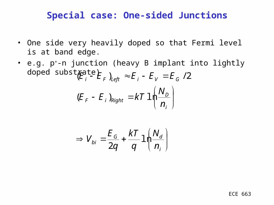
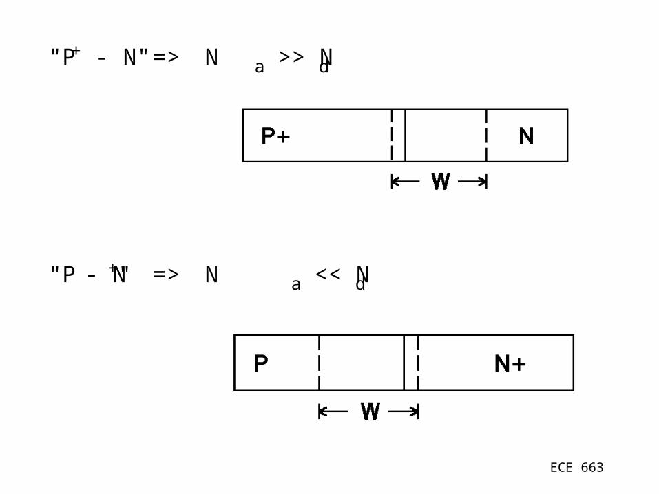
Special case: One-sided Junctions
• One side very heavily doped so that Fermi level is at band edge.
• e.g. p+-n junction (heavy B implant into lightly doped substrate)
i
dGbi
i
DRightiF
GViLeftFi
nN
qkT
qE
V
nN
kTEE
EEEEE
ln2
ln)(
2/)(

ECE 663
How wide is the depletion region?
kTEE
i
Fi
enp)(
kTEE
i
iF
enn)(
ECE 663
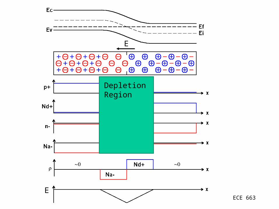
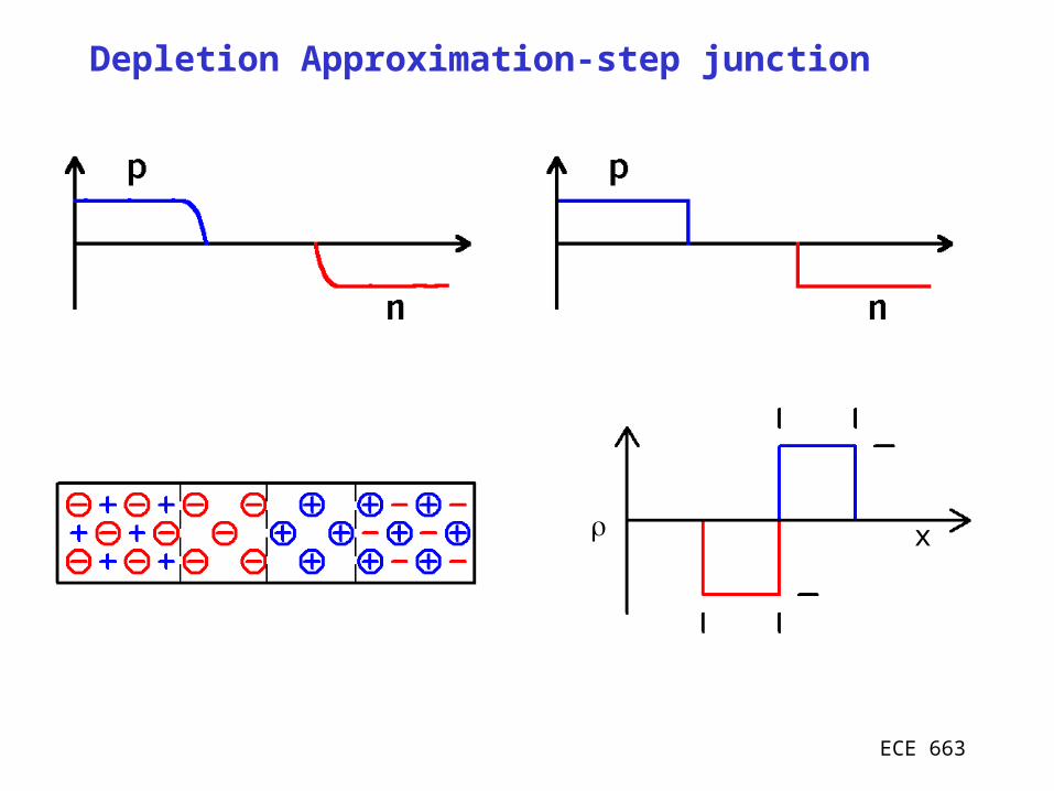
Depletion Approximation-step junction
x

ECE 663
Depletion approximation-step junction
Exponentials replaced with step-functions

ECE 663
Doping
ChargeDensity
Electric Field
ElectrostaticPotential
NAxp = NDxn
= WD/(NA-1 + ND
-1)
Ks0Em = -qNAxp = -qNDxn
= -qWD/(NA-1 + ND
-1)
Vbi = ½|Em|WD

ECE 663
Depletion Width
A
DAn
A
Dn
A
Dnnpn N
NNx
NN
xNN
xxxxW 1
21
0
21
0
2
2
biAD
DAS
A
DAbi
DAD
AS
VNN
NNq
KW
NNN
VNNN
Nq
KW
ECE 663
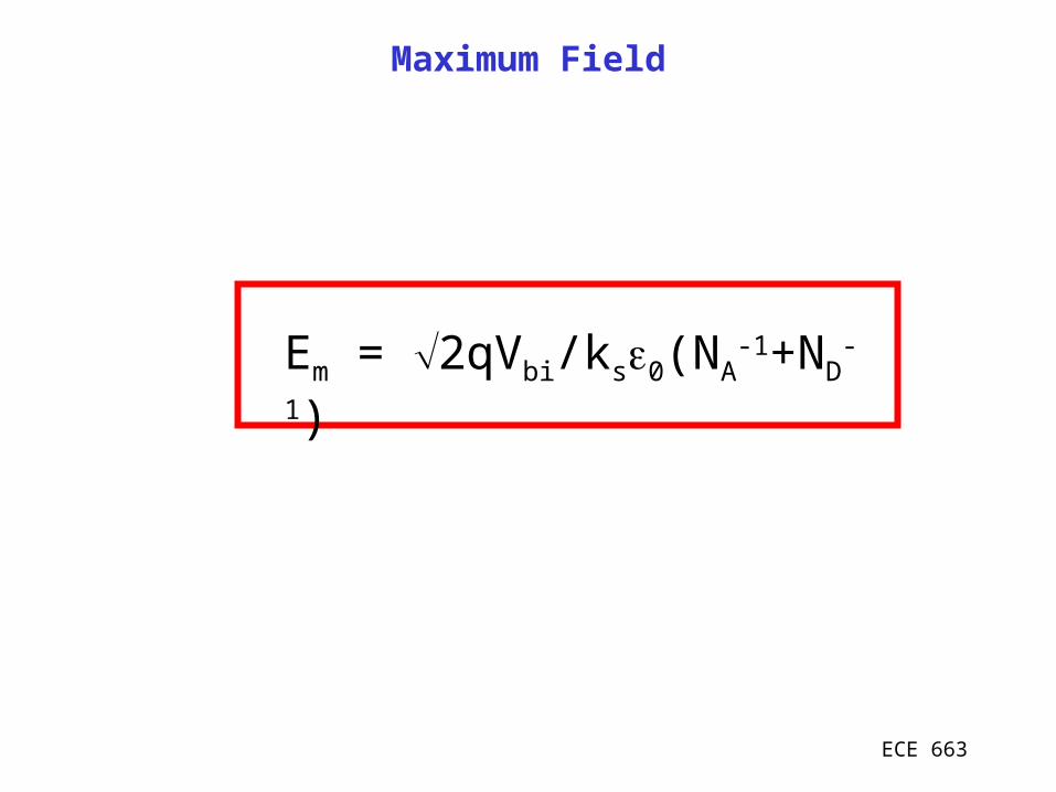
Maximum Field
Em = 2qVbi/ks0(NA-1+ND
-
1)

ECE 663
How far does Wd extend into each junction?
Depletion width on the n-side depends on the doping on the p-sideDepletion width on the p-side depends on the doping on the n-side
e.g. if NA>>ND then xn>>xp One-sided junction
DA
An
A
DAn
NNN
Wx
or
NNN
xW
DA
Dp
A
DA
D
Ap
A
DAn
NNN
Wx
or
NNN
NN
xN
NNxW
ECE 663
ECE 663
"P+ - N" => N a >> Nd => xp << xn
"P - N+" => N a << Nd => xp >> xn
ECE 663
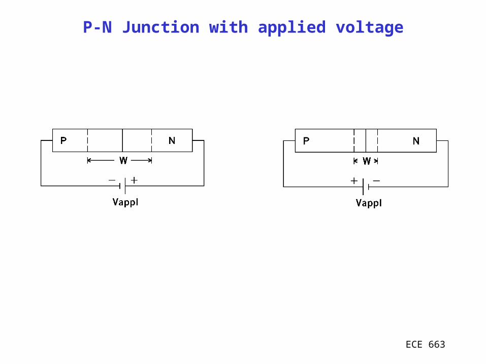
P-N Junction with applied voltage
ECE 663
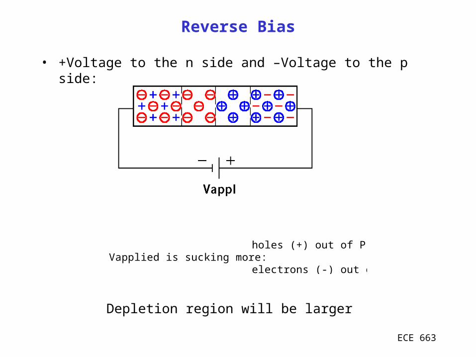
Reverse Bias
• +Voltage to the n side and –Voltage to the p side:
holes (+) out of P-sideVapplied is sucking more:
electrons (-) out of N-side
Depletion region will be larger

ECE 663
Reverse Bias Band Diagram

ECE 663
Reverse Bias depletion
2
1
02
revbi
AD
DAS VVNN
NNq
KW
DA
Arevn NN
NVWx
DA
Drevp NN
NVWx
Applied voltage disturbs equilibrium EF no longer constant
Reverse bias adds to the effect of built-in voltage

ECE 663
Forward Bias
+ -
Negative voltage to n side positive to p side
More electrons supplied to n, more holes to p
Depletion region gets smaller
ECE 663
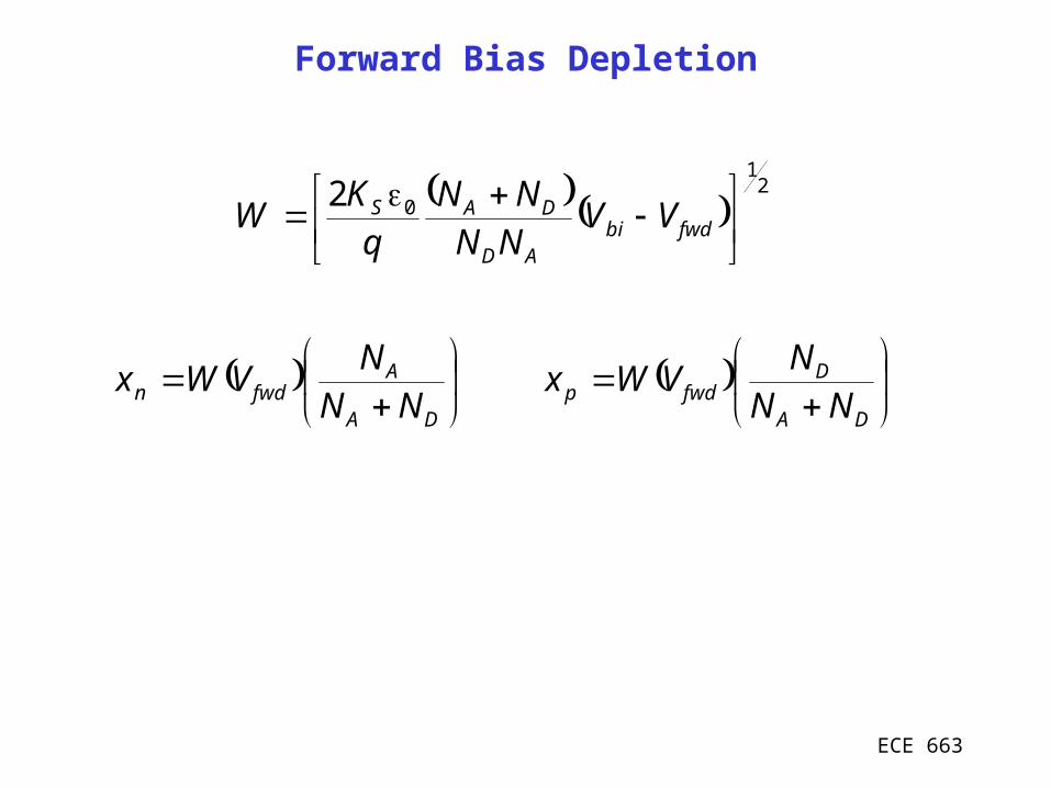
Forward Bias Depletion
2
1
02
fwdbi
AD
DAS VVNN
NNq
KW
DA
Afwdn NN
NVWx
DA
Dfwdp NN
NVWx
ECE 663
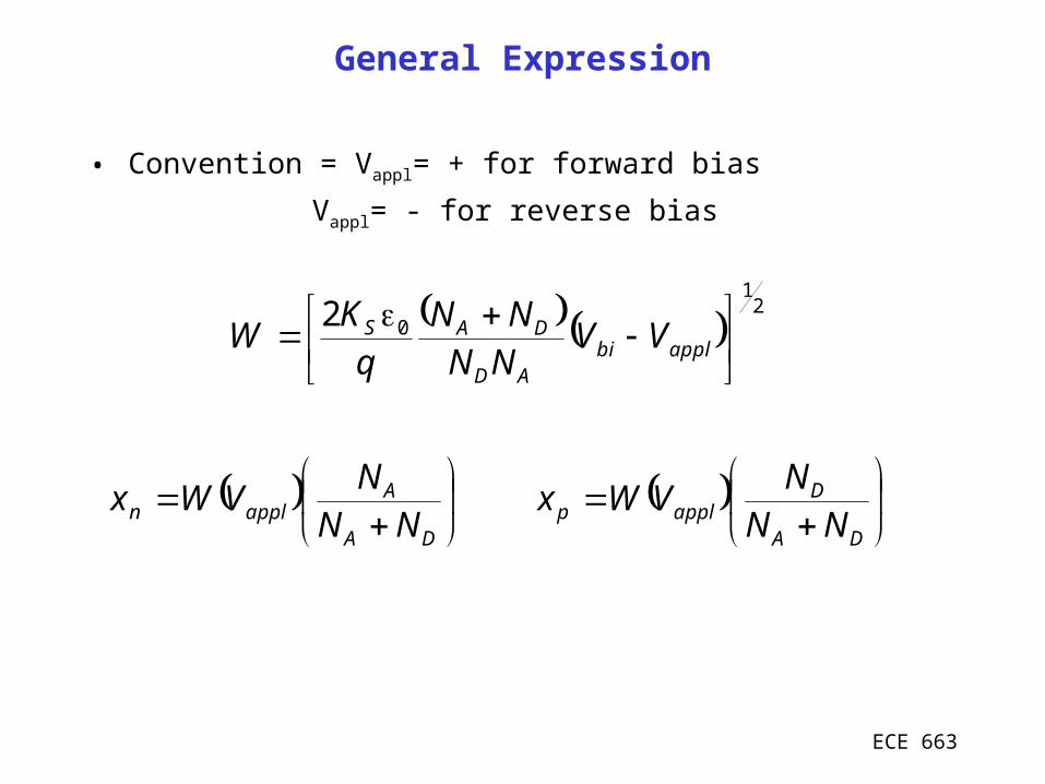
General Expression
• Convention = Vappl= + for forward bias
Vappl= - for reverse bias
2
1
02
applbi
AD
DAS VVNN
NNq
KW
DA
Aappln NN
NVWx
DA
Dapplp NN
NVWx

ECE 663
Bands = plots of electron energy
Voltage = potential energy per (+) charge
Positive voltage pulls bands down- bands are plots of electron energy
Fermi level is not constant Current Flow
Fn
Fpn = nie(Fn-Ei)/kT
p = nie(Ei-Fp)/kT
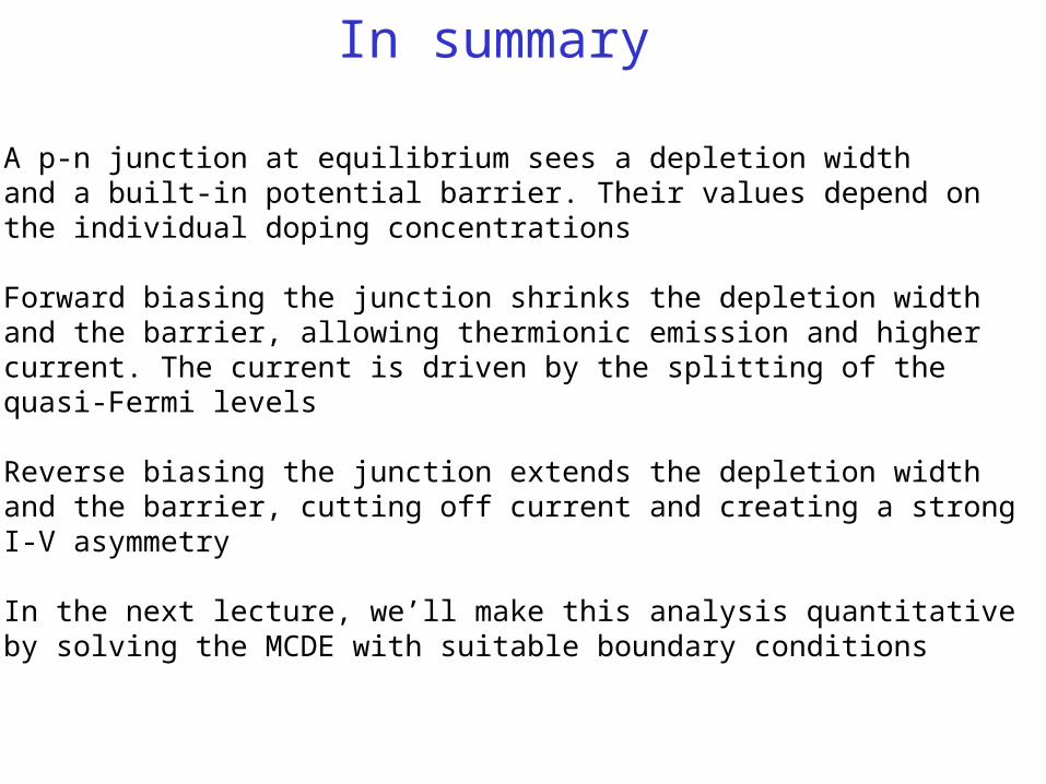
In summary
A p-n junction at equilibrium sees a depletion widthand a built-in potential barrier. Their values depend on the individual doping concentrations
Forward biasing the junction shrinks the depletion widthand the barrier, allowing thermionic emission and highercurrent. The current is driven by the splitting of the quasi-Fermi levels
Reverse biasing the junction extends the depletion widthand the barrier, cutting off current and creating a strongI-V asymmetry
In the next lecture, we’ll make this analysis quantitative by solving the MCDE with suitable boundary conditions


![Culminating Project.Pointer.Fisher[1]](https://img.pdfslide.us/doc/110x75/554fde1ab4c905264d8b4c75/culminating-projectpointerfisher1.jpg)
