Embed Size (px)
Citation preview

ECE 663
Ideal Diode I-V characteristic

ECE 663
Real Diode I-V characteristic

ECE 663
Real Diode – Forward Bias (semi-log scale)
ECE 663
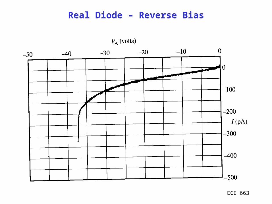
Real Diode – Reverse Bias

ECE 663
What’s wrong with this picture?
• Forward Bias– For V < 0.35 volts slope is kT/2q– For 0.35V < V < 0.7volts, slope is kT/q
– For V > 0.7 volts, slope less than kT/q (V~Vbi)
– I0 ~10-14A from intercept of semi-log plot in FB

ECE 663
What’s wrong with this picture?
• Reverse Bias– Current ~103 times larger than FB I0– Reverse current doesn’t saturate
– Breakdown – large current above Vbd
• Avalanche breakdown• Zener (tunneling) process

ECE 663
Reverse Bias Avalanche Breakdown
Depletion width larger than mean free path lots of collisions

ECE 663
Avalanching
• Minority carriers accelerated by electric field in depletion region
• The average energy lost per collision goes up as E field (voltage) goes up (v = E )
• At some critical field (Ec), the average energy lost per collision will be enough to “ionize” lattice atoms – knock out more carriers
• Those carriers will also be accelerated by E>Ec and make more carriers when they collide, etc…….
• Many collisions=huge multiplication in number of carriers= avalanche breakdown

ECE 663
Max. FieldDoping
ChargeDensity
Electric Field
ElectrostaticPotential
NAxp = NDxn
= WD/(NA-1 + ND
-1)
Ks0Em = -qNAxp = -qNDxn
= -qWD/(NA-1 + ND
-1)
Vbi = ½|Em|WD

ECE 663
Maximum Field
Em = 2qVbi/ks0(NA-1+ND
-
1)

ECE 663
Avalanching
BBR
DA
DABR
BRDA
DA
Sc
BRBRbiAbi
NV
NNNN
V
VNN
NNK
qE
VVVVV
1
2
0
2
One-sided junctions

ECE 663
Experimental Data on VBR
75.0
1
B
BRN
V

ECE 663
Zener Breakdown - Tunneling
Barrier must be thin: depletion is narrow doping on both sides must be large
Must have empty states to tunnel into Vbi + VBR > EG/q
2
1
02
applbi
AD
DAS VVNNNN
qK
W

ECE 663
Zener diode I-V characteristic

ECE 663
Reverse bias R-G in the depletion region
n
p
x
xGR
thermalGR dx
tn
qAI

ECE 663
R-G Current
• In depletion region we don’t have low level injection because number of carriers is small and injected carriers is large
n
p
x
x pp
iGR
pp
i
GRthermal
dxppnn
nnpqAI
ppnnnnp
tn
)()(
)()(
11
2
11
2
But, in depletion n,p 0
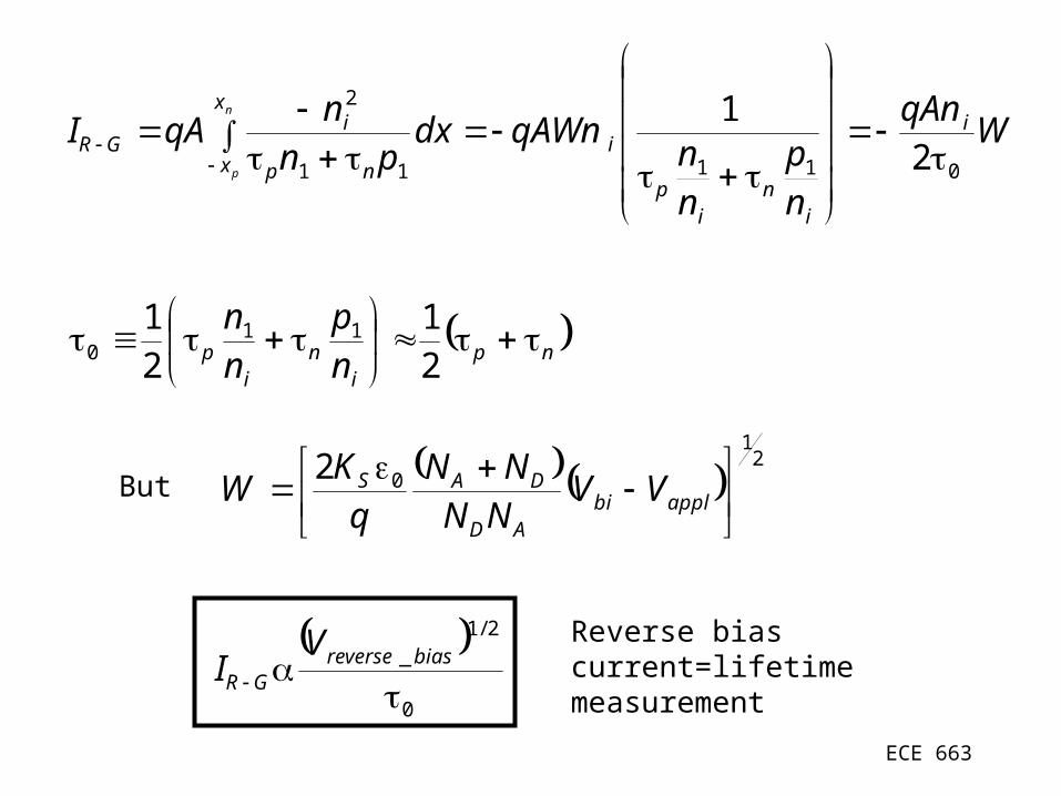
ECE 663
npi
ni
p
x
x
i
in
ip
inp
iGR
np
nn
WqAn
np
nn
qAWndxpn
nqAI
n
p
21
21
21
110
01111
2
2
1
02
applbi
AD
DAS VVNNNN
qK
WBut
0
2/1_
biasreverseGR
VI
Reverse bias current=lifetime measurement

ECE 663
Forward Bias R-G

ECE 663
Forward Bias R-G current
n and p cannot be neglected in the depletion region in FB so the integral is not so easy as in RB.
n
p
x
x pp
iGR dx
ppnnnnp
qAI)()( 11
2
0
11
/2/00
pn
i
kTqVi
kTqVnnnn
npn
enenpnp
n
p
x
x inn
kTqVi
GR dxnpn
enqAI
)2(1
0
/2
Estimate value of integral using maximum value of integrand = constant

ECE 663
Forward Bias R-G current
n
p
x
x inn
kTqVi
GR dxnpn
enqAI
)2(1
0
/2
Integrand maximum when n + p is minimum or n = p
kTqVinnnn
kTqVinn
enpnpn
enpn2/
/2
kTqViGR
kTqV
kTqVi
GR
x
xikTqV
ikTqV
i
kTqVi
GR
eWqAn
I
een
qAI
dxnenen
enqAI
n
p
2/
0
2/0
/
2/2/0
/2
2
)1(21
)2(1
W

ECE 663
Ideality factor
kTqVeII /0

Forward Bias with High Currents: High Level injection
np = ni2eqV/kT
n ~ p ≈ nieqV/2kT
Use in boundary condition

ECE 663
Forward Bias with High Currents: Series Resistance
I = I0[eqV/kT-1]
I = I0[eq(V-IRs)/kT-1]

ECE 663
Real Diode I-V curve summary
A. Breakdown (VB~1/NB)B. R-G RB (I~V)C. R-G FB (slope~q/2kT)D. High Level Inj.(slope ~ q/2kT)E. Series Resistance – slope over

ECE 663
Narrow Base P-N junction Diode
P-side N-side
np pn
LpLn
xnxp
What happens if the diode is smaller than the minority carrier diffusionlength(s)?
Diffusion lengths can be 20-30 microns

ECE 663
1/0 kTqV
n
npnpp e
W
pqD
dxpd
qDJ
Similarly for Jn
1/0 kTqV
p
pnn e
W
nqDJ

ECE 663
Total diode current
1/00
kTqV
n
np
p
pnpntotal e
W
pqD
W
nqDJJJ
Compare to result from wide base ideal diode:
1/00
kTqV
p
np
n
pn eL
pqD
L
nqDJ
Replace minority carrier diffusion length with diode width
pn WL np WL

ECE 663
Charge control methodology
x -xp
np
• Analyze by examining injected minority carrier charge:• e.g. electrons injected into p side of FB diode
• Total negative charge on p-side:
nnn
LxxkTqVpppp
DL
eennnn np
//00 1
px
pnegativetotal AqdxxnQ )(

ECE 663
Charge control method
• Approximate total charge by diffusion length times charge at boundary of QN-depletion regions:
• Non-equilibrium injected electrons with average lifetime of n
• Recombination Rate=charge/time=current
AqenLQ kTqVpnnegativetotal 1/
0
1
1/
/0
/0
kTqV
n
pnn
nkTqV
n
pnnn
enL
qJ
AJenL
qAQI

ECE 663
Charge control
n
n
nn
n
n
n
n
nn
n
n
LD
DDDDL
1/0
kTqV
n
pnn e
L
nDqJ
but
Similarly for holes on the n-side:
1/0
kTqV
p
npp e
L
pDqJ

ECE 663
Total current:
• Same result as before but we didn’t have to solve the minority carrier diffusion equations
• Stored charge and recombination = current needed to resupply
1/00
kTqV
p
np
n
pnpn e
L
pD
L
nDqJJJ