Embed Size (px)
Citation preview

ECE 1352F (2003)Analog Circuit Design
Presentation
Integrated “Smart Power” IGBT Drivers
Kay (Tsz Shuen) Chan993509681November 28, 2003

Objectives
Introduce briefly some of the design considerations of IGBT drivers in power electronics
Present recent design techniques and circuits for IGBT driver
Address future challenges in IGBT driver design
“Smart Power” IC
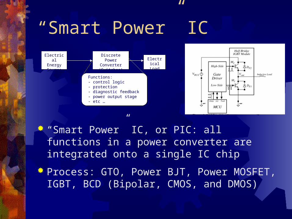
“Smart Power” IC, or PIC: all functions in a power converter are integrated onto a single IC chip
Process: GTO, Power BJT, Power MOSFET, IGBT, BCD (Bipolar, CMOS, and DMOS)
Electrical Energy Source
Discrete Power Converter (Switches)
Electrical Load
Functions:- control logic- protection- diagnostic feedback- power output stage- etc …
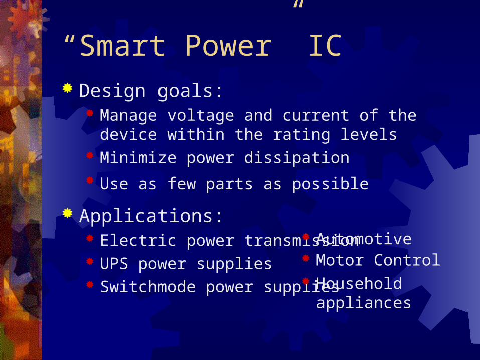
“Smart Power” IC Design goals:
Manage voltage and current of the device within the rating levels
Minimize power dissipation Use as few parts as possible
Applications: Electric power transmission UPS power supplies Switchmode power supplies
Automotive Motor Control Household appliances
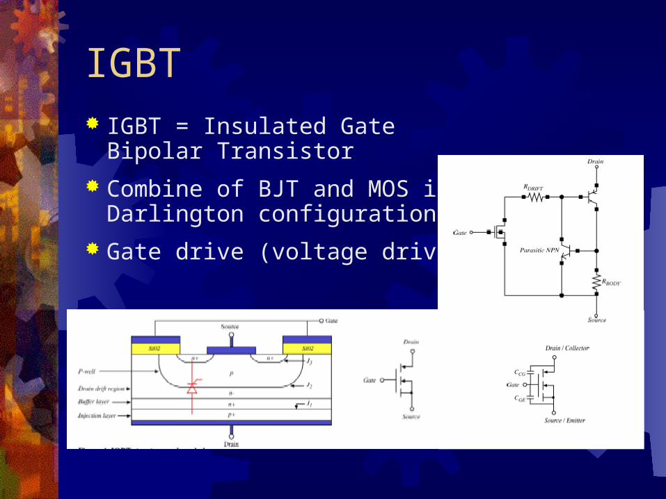
IGBT IGBT = Insulated Gate Bipolar
Transistor
Combine of BJT and MOS in Darlington configuration
Gate drive (voltage drive)

IGBT: Switches in PIC Compared to BJT and Power-MOS, IGBT has
Higher on-state voltage and current density Higher input impedance Rapid switching times Lower conduction losses Less silicon area because the gate driver circuit is
simpler
Becomes a popular switching device in medium and high power applications (>100W)
To increase voltage rating (>1000V), need to use series-connected IGBTs

IGBT: Switching Characteristics
Switching losses
Overvoltage (VCE,overvoltage)
Overcurrent (IRR)
IGBT: Switching Losses
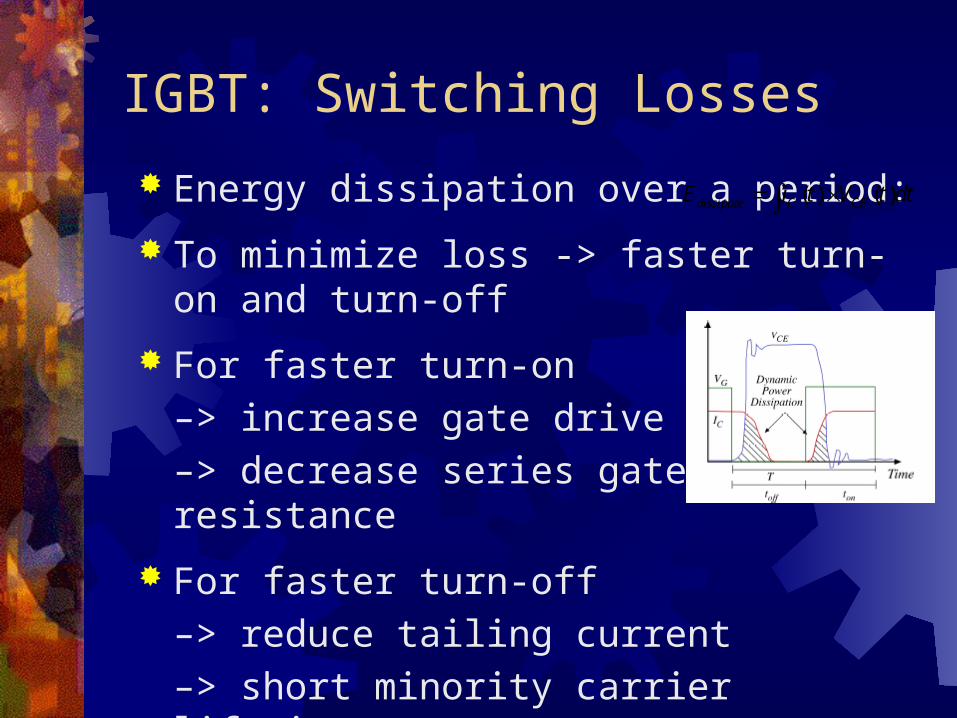
Energy dissipation over a period:
To minimize loss -> faster turn-on and turn-off
For faster turn-on
–> increase gate drive voltage
–> decrease series gate resistance
For faster turn-off
–> reduce tailing current
–> short minority carrier lifetime
( ) ( )dissipate C CEE i t V t dt

IGBT: Safe Operating Area
Current and voltage boundary within which the IGBT can be operated without destructive failure
Long duration of simultaneous high voltage and current across IGBT leads to thermal breakdown
–> Reduce overcurrent and overvoltage
–> Imply slower turn-on and turn off!!
Trade-off between speed (switching losses) and overshoot voltage (circuit reliability)
02RRon
diI I
dt
,CE overvoltage S
off
diV L
dt
Gate Driver Design Techniques
Reduce IRR (diode reverse recovery current) by: reducing di/dt, which means increasing gate
series resistances
Reduce VCE,overvoltage by reducing di/dt balancing gate timing and voltage sharing
among the series-connected IGBTs
In both cases, need a better, independent control of di/dt and dv/dt to optimize the gate driver for speed, minimum losses, and reliability

Two-Stage Gate Driver To reduce IRR and VCE,overvoltage , [6] suggested the
following two-stage driver circuit Turn-on:
RGon2 << RGon1
Stage-2 is off initially Cgate charged through RGon1
(larger) to keep IRR small After diode has recovered, stage-2 turn on (triggered
by VREF in comparator) Driver resistance is now
RGon1||RGon2 (smaller)
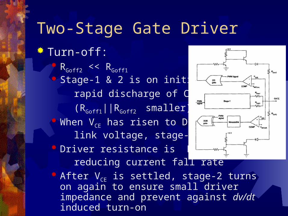
Two-Stage Gate Driver Turn-off:
RGoff2 << RGoff1
Stage-1 & 2 is on initially for
rapid discharge of Cgate
(RGoff1||RGoff2 smaller) When VCE has risen to DC, link voltage, stage-2 turns off Driver resistance is RGoff1, reducing current fall rate After VCE is settled, stage-2 turns on again to ensure
small driver impedance and prevent against dv/dt induced turn-on
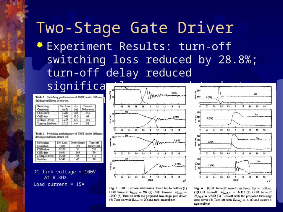
Two-Stage Gate Driver Experiment Results: turn-off switching loss
reduced by 28.8%; turn-off delay reduced significantly compared to just increasing gate resistance
DC link voltage = 100V at 8 kHz
Load current = 15A
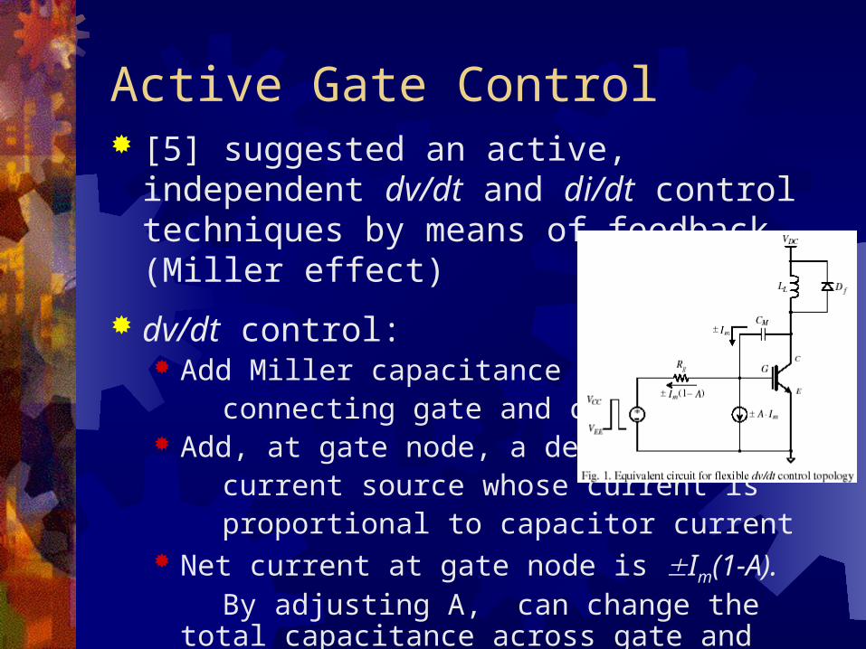
Active Gate Control [5] suggested an active, independent dv/dt and
di/dt control techniques by means of feedback (Miller effect)
dv/dt control: Add Miller capacitance connecting gate and collector Add, at gate node, a dependent current source whose current is proportional to capacitor current Net current at gate node is Im(1-A). By adjusting A, can change the total capacitance
across gate and collector, and thus changing dv/dt
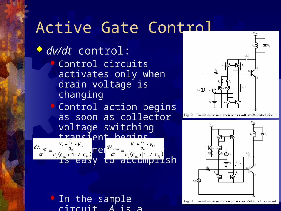
Active Gate Control dv/dt control:
Control circuits activates only when drain voltage is changing
Control action begins as soon as collector voltage switching transient begins
Adjustments of dv/dt is easy to accomplish
In the sample circuit, A is a linear function of Vc
,
1
LT EE
CE off m
g gc M
IV V
dV g
dt R C A C
,
1
LT CC
CE on m
g gc M
IV V
dV g
dt R C A C
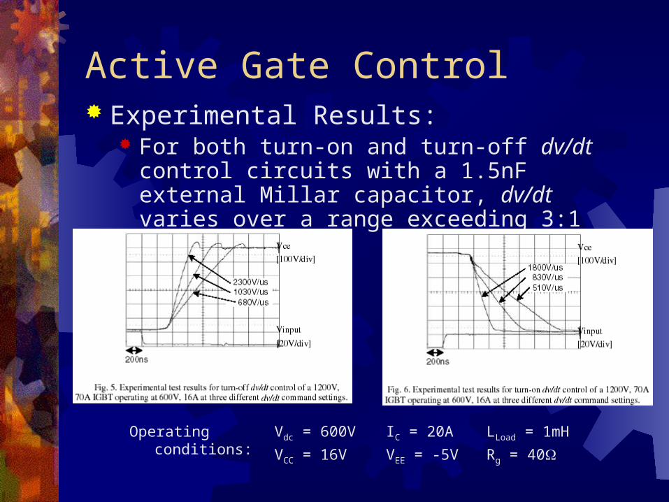
Active Gate Control Experimental Results:
For both turn-on and turn-off dv/dt control circuits with a 1.5nF external Millar capacitor, dv/dt varies over a range exceeding 3:1
Vdc = 600V
VCC = 16V
IC = 20A
VEE = -5V
LLoad = 1mH
Rg = 40
Operating conditions:

Active Gate Control di/dt control:
Dual version of dv/dt -> add external inductance LS connecting in series with switch emitter
Experimental Results: Again, for both turn-on
and turn-off di/dt control circuits with a 80nH external inductance, di/dt varies over a range exceeding 3:1

Voltage Balancing Different switching time of the IGBTs in series
leads to imbalance of voltage share, resulting in overvoltage at turn-off
Overvoltage can be reduced by matching the switching time and balancing the voltage share

Voltage Balancing [7] suggested a multi-level
clamp and turn-off timing adjustment driver to balance the voltage
Overvoltage reduces from 3700V to 3300V
Turn-off timings within 100ns
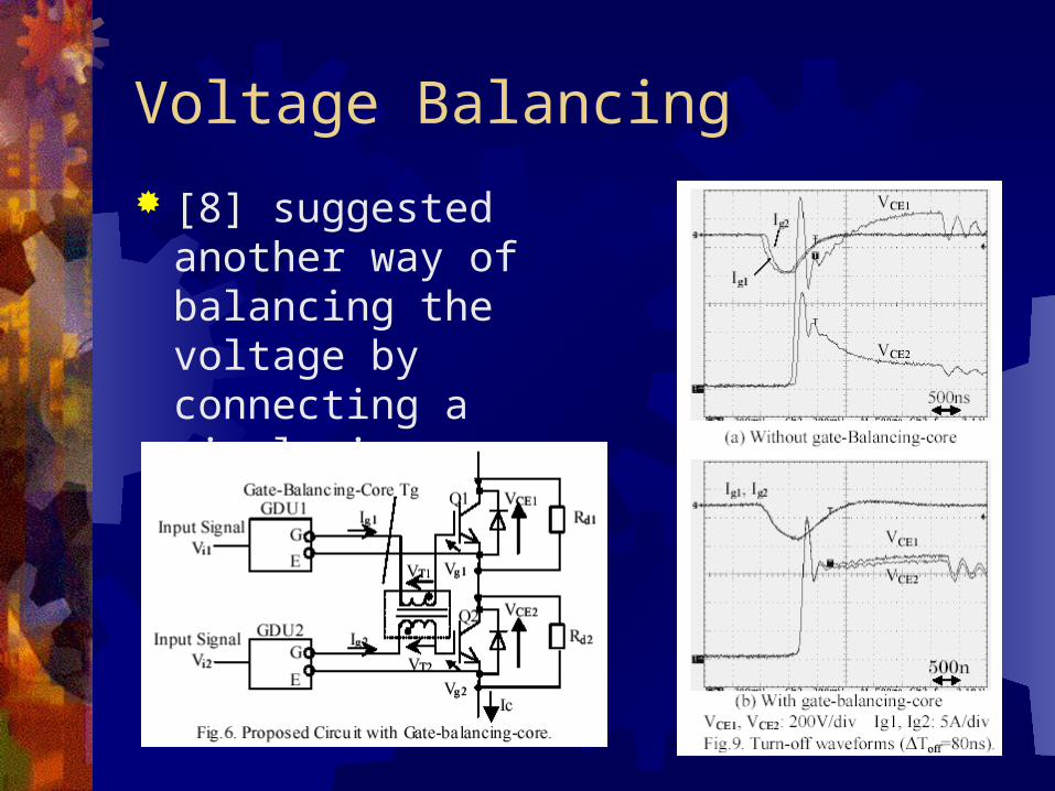
Voltage Balancing
[8] suggested another way of balancing the voltage by connecting a simple iron core and coils at the gate
Future Challenges How to best utilize the control techniques in
future generations of gate drive circuits
In particular, how to optimize the gate drive circuits for a even better timing and switching losses while keeping the circuits compact
As the voltage and current ratings increase, new techniques are in need to ensure circuit protection and reliability

Future Challenges Recent IEEE papers have presented analysis of
IGBT operation under short-circuit, over temperature, hard switching fault, and fault under load conditions
(next step -> gate drive circuits realization)
IGBT process has been evolving, leading to new concerns in gate driver design

References ECE1352 Term Papers:[1] O. Trescases, “ECE1352 Term Paper: Integrated “Smart Power”
IGBT Drivers”, 2003.
IGBT Process:[2] M. H. Rashid, Power Electronics Handbook, San Diego: Academic
Press, 2001.
[3] N. Kularatna, Power Electronics Design Handbook: Low-Power Components and Applications, Boston: Newnes, 1998.
IGBT Gate Drive:[4] R.S. Chokhawala, J. Catt, and B.R. Pelly, “Gate Drive
Considerations for IGBT Modules,” Industry Applications, IEEE Transactions on, vol. 31, no. 3, pp. 603-611, May-June 1995.
References IGBT Gate Drive:[5] S. Park and T. M. Jahns, “Flexible dv/dt and di/dt Control Method for
Insulated Gate Power Switches,” Industry Applications Conference, 2001. 36th IAS Annual Meeting. Conference Record of the 2001 IEEE, vol. 2, pp. 1038-1045, Sept-Oct 2001.
[6] R. Sachdeva and E. P. Nowicki, “A Novel Gate Driver Circuit for Snubberless, Low-Noise Operation of High Power IGBT,” Electrical and Computer Engineering, 2002. IEEE CCECE 2002. Canadian Conference, vol. 1, pp. 212-217, May 2002.
[7] H. Nakatake and A. Iwata, “Series Connection of IGBTs used Multi-Level Clamp Circuit and Turn Off Timing Adjustment Circuit,” Power Electronics Specialist, 2003. PESC '03. IEEE 34th Annual Conference, vol. 4, pp. 1910-1915, June 2003.
[8] K. Sasagawa, Y. Abe, and K. Matsuse, “Voltage Balancing Method for IGBTs Connected in Series,” Industry Applications Conference, 2002. 37th IAS Annual Meeting. Conference Record, vol. 4, pp. 2597-2602, Oct 2002.