Embed Size (px)
Citation preview

EC2SB 10W Isolated DC-DC Converters
Application Note V12 November 2020
1
ISOLATED DC-DC Converter
EC2SB SERIES
APPLICATION NOTE
Approved By:
Department Approved By Checked By Written By
Research and Development Department
Enoch Tim Joyce
Jacky
Quality Assurance Department
Ryan Benny

EC2SB 10W Isolated DC-DC Converters
Application Note V12 November 2020
2
Content
1. INTRODUCTION 3
2. DC-DC CONVERTER FEATURES 3
3. ELECTRICAL BLOCK DIAGRAM 3
4. TECHNICAL SPECIFICATIONS 5
5. MAIN FEATURES AND FUNCTIONS 10 5.1 Operating Temperature Range 10
5.2 Over Current Protection 10
5.3 Remote On/Off 10
6. APPLICATIONS 10 6.1 Recommended Layout PCB Footprints and Soldering Information 10
6.2 Power De-Rating Curves for EC2SB Series 11
6.3 Efficiency vs. Load Curves 12
6.4 Input Capacitance at the Power Module 17
6.5 Test Set-Up 17
6.6 Output Voltage Adjustment 17
6.7 Output Ripple and Noise Measurement 18
6.8 Output Capacitance 18
7. SAFETY & EMC 19 7.1 Input Fusing and Safety Considerations. 19
7.2 EMC Considerations 19
8. PART NUMBER 25
9. MECHANICAL SPECIFICATIONS 25

EC2SB 10W Isolated DC-DC Converters
Application Note V12 November 2020
3
1. Introduction The EC2SB series offer 10 watts of output power in a
1.00x1.00x0.4 inches Copper packages. The EC2SB
series has a 2:1 wide input voltage range of 4.7-9, 9-18,
18-36 and 36-75VDC and provides a precisely
regulated output. This series has features such as high
efficiency, 1500VDC of isolation and allows an ambient
operating temperature range of –40°C to 85°C
(de-rating above 71 °C). The features include short
circuit protection and remote on/off control. All models
are very suitable for distributed power architectures,
telecommunications, battery operated equipment and
industrial applications.
2. DC-DC Converter Features 10W Isolated Output
Efficiency to 87%
2:1 Input Range
Regulated Outputs
Fixed Switching Frequency
Input under-voltage Protection
Over Current Protection
Remote On/Off
Continuous Short Circuit Protection
Conductive EMI Meets EN55032 Class A
Without Tantalum Capacitors Inside
Safety Meets IEC/EN/UL 62368-1
3. Electrical Block Diagram
Figure 1 Electrical Block Diagram for Single Output Modules
+VIN
-VIN
ON/OFF CONTROL
-VOUT
TRIM
+VOUT
SWITCH
CONTROL
UVLOCOMPARATORS
PWMCONTROLLER
OPTOISOLATION
REFERENCE& ERROR AMP
(1)
(2)
(6)
(3)
(5)
(4)

EC2SB 10W Isolated DC-DC Converters
Application Note V12 November 2020
4
Figure 2 Electrical Block Diagram for Dual Output Modules

EC2SB 10W Isolated DC-DC Converters
Application Note V12 November 2020
5
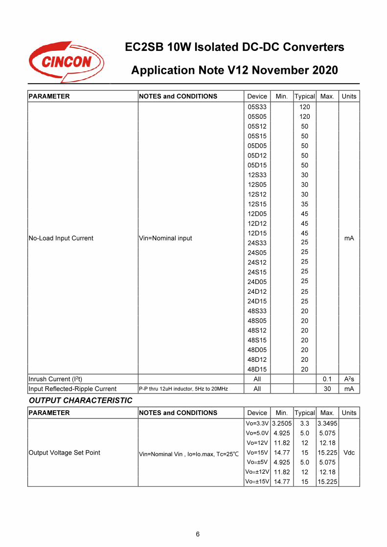
4. Technical Specifications (All specifications are typical at nominal input, full load at 25 unless otherwise noted.)
ABSOLUTE MAXIMUM RATINGS
PARAMETER NOTES and CONDITIONS Device Min. Typical Max. Units
Input Voltage
Continuous
05SXX -0.3 9
Vdc 12SXX -0.3 18
24SXX -0.3 36
48SXX -0.3 75
Transient 100ms
05SXX 12
Vdc 12SXX 25
24SXX 50
48SXX 100
Operating Ambient Temperature De-rating, Above 71 All -40 +85
Case Temperature All 105
Storage Temperature All -55 +125
Input/Output Isolation Voltage 1 minute All 1500 Vdc
INPUT CHARACTERISTICS
PARAMETER NOTES and CONDITIONS Device Min. Typical Max. Units
Operating Input Voltage
05SXX 4.7 5 9
Vdc 12SXX 9 12 18
24SXX 18 24 36
48SXX 36 48 75
Turn-On Voltage Threshold
05SXX 4.2 4.4 4.6
Vdc 12SXX 8.4 8.8 9.2
24SXX 16.5 17 17.5
48SXX 33.5 34 34.5
Turn-Off Voltage Threshold
05SXX 4 4.2 4.4
Vdc 12SXX 7.7 8 8.3
24SXX 15.5 16 16.7
48SXX 31.5 32 32.5
Lockout Hysteresis Voltage
05SXX 0.3
Vdc 12SXX 0.5
24SXX 1
48SXX 1
Maximum Input Current
100% Load, Vin=4.7V for 05XXX 05SXX 2700
mA 100% Load, Vin=9V for 12XXX 12SXX 1350
100% Load, Vin=18V for 24XXX 24SXX 675
100% Load, Vin=36V for 48XXX 48SXX 338
EC2SB 10W Isolated DC-DC Converters
Application Note V12 November 2020
6
PARAMETER NOTES and CONDITIONS Device Min. Typical Max. Units
No-Load Input Current Vin=Nominal input
05S33 120
mA
05S05 120
05S12 50
05S15 50
05D05 50
05D12 50
05D15 50
12S33 30
12S05 30
12S12 30
12S15 35
12D05 45
12D12 45
12D15 45
24S33 25
24S05 25
24S12 25
24S15 25
24D05 25
24D12 25
24D15 25
48S33 20
48S05 20
48S12 20
48S15 20
48D05 20
48D12 20
48D15 20
Inrush Current (I2t) All 0.1 A2s
Input Reflected-Ripple Current P-P thru 12uH inductor, 5Hz to 20MHz All 30 mA
OUTPUT CHARACTERISTIC
PARAMETER NOTES and CONDITIONS Device Min. Typical Max. Units
Output Voltage Set Point Vin=Nominal Vin , Io=Io.max, Tc=25
Vo=3.3V 3.2505 3.3 3.3495
Vdc
Vo=5.0V 4.925 5.0 5.075
Vo=12V 11.82 12 12.18
Vo=15V 14.77 15 15.225
Vo=±5V 4.925 5.0 5.075
Vo=±12V 11.82 12 12.18
Vo=±15V 14.77 15 15.225
EC2SB 10W Isolated DC-DC Converters
Application Note V12 November 2020
7
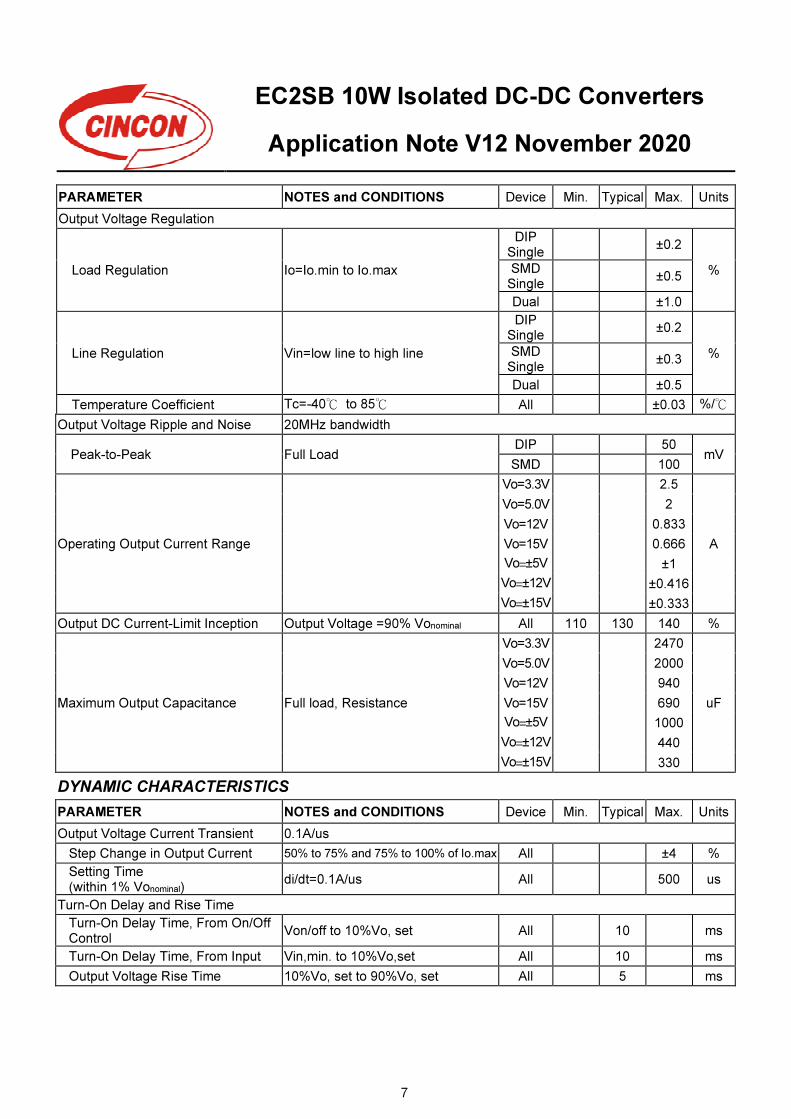
PARAMETER NOTES and CONDITIONS Device Min. Typical Max. Units
Output Voltage Regulation
Load Regulation Io=Io.min to Io.max
DIP Single
±0.2
% SMD Single
±0.5
Dual ±1.0
Line Regulation Vin=low line to high line
DIP Single
±0.2
% SMD Single
±0.3
Dual ±0.5
Temperature Coefficient Tc=-40 to 85 All ±0.03 %/
Output Voltage Ripple and Noise 20MHz bandwidth
Peak-to-Peak Full Load DIP 50
mV SMD 100
Operating Output Current Range
Vo=3.3V 2.5
A
Vo=5.0V 2
Vo=12V 0.833
Vo=15V 0.666
Vo=±5V ±1
Vo=±12V ±0.416
Vo=±15V ±0.333
Output DC Current-Limit Inception Output Voltage =90% Vonominal All 110 130 140 %
Maximum Output Capacitance Full load, Resistance
Vo=3.3V 2470
uF
Vo=5.0V 2000
Vo=12V 940
Vo=15V 690
Vo=±5V 1000
Vo=±12V 440
Vo=±15V 330
DYNAMIC CHARACTERISTICS
PARAMETER NOTES and CONDITIONS Device Min. Typical Max. Units
Output Voltage Current Transient 0.1A/us
Step Change in Output Current 50% to 75% and 75% to 100% of Io.max All ±4 %
Setting Time (within 1% Vonominal)
di/dt=0.1A/us All 500 us
Turn-On Delay and Rise Time
Turn-On Delay Time, From On/Off Control
Von/off to 10%Vo, set All 10 ms
Turn-On Delay Time, From Input Vin,min. to 10%Vo,set All 10 ms
Output Voltage Rise Time 10%Vo, set to 90%Vo, set All 5 ms

EC2SB 10W Isolated DC-DC Converters
Application Note V12 November 2020
8
EFFICIENCY
PARAMETER NOTES and CONDITIONS Device Min. Typical Max. Units
100% Load
05S33 87
%
05S05 87
05S12 87
05S15 87
05D05 85
05D12 87
05D15 87
12S33 82
12S05 85
12S12 87
12S15 87
12D05 85
12D12 87
12D15 87
24S33 82
24S05 85
24S12 87
24S15 87
24D05 85
24D12 87
24D15 87
48S33 81
48S05 85
48S12 87
48S15 87
48D05 85
48D12 87
48D15 87
ISOLATION CHARACTERISTICS
PARAMETER NOTES and CONDITIONS Device Min. Typical Max. Units
Input to Output 1 minutes All 1500 Vdc
Isolation Resistance All 1000 MΩ
Isolation Capacitance All 1000 pF
FEATURE CHARACTERISTICS
PARAMETER NOTES and CONDITIONS Device Min. Typical Max. Units
Switching Frequency All 350 KHz

EC2SB 10W Isolated DC-DC Converters
Application Note V12 November 2020
9
PARAMETER NOTES and CONDITIONS Device Min. Typical Max. Units
On/Off Control, Positive Remote On/Off logic
Logic Low (Module Off) Von/off at Ion/off=1.0mA All 0 1.2 V
Logic High (Module On) Von/off at Ion/off=0.1uA All 5.5 or open circuit
75 V
On/Off Control, Negative Remote On/Off logic
Logic High (Module On) Von/off at Ion/off=1.0mA All N/A V
Logic Low (Module Off) Von/off at Ion/off=0.0uA All N/A V
On/Off Current (for both remote on/off logic)
Ion/off at Von/off=0.0V All 1 mA
Leakage Current (for both remote on/off logic)
Logic High, Von/off=15V All 30 uA
Off Converter Input Current Shutdown input idle current
5Vin 24Vin 48Vin
5 10 mA
12Vin 10 15
Output Voltage Trim Range Pout=max rated power All -10 +10 %
Output Over Voltage Protection
Vo=3.3V 3.9
V
Vo=5.0V 6.2
Vo=12V 15
Vo=15V 18
Vo=±5V ±6.2
Vo=±12V ±15
Vo=±15V ±18
Over-Temperature Shutdown All N/A
GENERAL SPECIFICATIONS
PARAMETER NOTES and CONDITIONS Device Min. Typical Max. Units
MTBF Io=100% of Io_max; Ta=25 per
MIL-HDBK-217F_Notice 1, GBAll 1.2
M hours
Weight All 18 grams

EC2SB 10W Isolated DC-DC Converters
Application Note V12 November 2020
10
5. Main Features and Functions 5.1 Operating Temperature Range
The EC2SB series converters can be operated by a
wide ambient temperature range from -40 to 85
(de-rating above 71) The standard model has a
Copper case and case temperature can not over 105
at normal operating. 5.2 Over Current Protection
All different voltage models have full continuous short-circuit protection. To provide protection in a fault condition, the unit is equipped with internal over-current protection. The unit operates normally once the fault condition is removed. At the point of current-limit inception, the converter will go into over current protection.
5.3 Remote On/Off
The EC2SB series allows the user to switch the module on and off electronically with the remote on/off feature. All models are available in “positive logic” versions. The converter turns on if the remote on/off pin is high (>5.5Vdc to 75Vdc or open circuit). Setting the pin low (0 to <1.2Vdc) will turn the converter off. The signal level of the remote on/off input is defined with respect to ground. If not using the remote on/off pin, leave the pin open (converter will be on).
6. Applications
6.1 Recommended Layout PCB Footprints and Soldering Information
The system designer or the end user must ensure that other components and metal in the vicinity of the converter meet the spacing requirements to which the system is approved. Low resistance and low inductance PCB layout traces are the norm and should be used where possible. Due consideration must also be given to proper low impedance tracks between power module, input and output grounds. The recommended footprints and soldering profiles are shown as Figure 3.
Note: Dimensions are in inches (millimeters)
Lead Free Wave Soldering Profile
0
50
100
150
200
250
300
0 50 100 150
Time (Seconds)
Tem
per
ature
( C
)
Note:
1. Soldering Materials: Sn/Cu/Ni
2. Ramp up rate during preheat: 1.4 /Sec (From 50
to 100)
3. Soaking temperature: 0.5 /Sec (From 100 to
130), 60±20 seconds
4. Peak temperature: 260, above 250 3~6 Seconds
5. Ramp up rate during cooling: -10.0 /Sec (From
260 to 150)
Figure3 Recommended PCB Layout Footprints and Wave Soldering Profiles for SB packages

EC2SB 10W Isolated DC-DC Converters
Application Note V12 November 2020
11
6.2 Power De-Rating Curves for EC2SB Series
Operating Ambient temperature Range: -40 ~ 71 without de-rating.
Maximum case temperature under any operating condition should not exceed 105.
Typical Derating curve for Natural Convection
-40
105
71
0%
20%
40%
60%
80%
100%
120%
-40 -20 0 20 40 60 80 100
Ambient Temperature(oC)
LOAD(%
)
Natural
Convection

EC2SB 10W Isolated DC-DC Converters
Application Note V12 November 2020
12
6.3 Efficiency vs. Load Curves
EC2SB-05S33 (Eff Vs Io)
40%
50%
60%
70%
80%
90%
100%
10% 20% 30% 40% 50% 60% 70% 80% 90% 100%
Current Load (%)
Effic
iency
(%
)
4.7V
5V
9V
EC2SB-05S05 (Eff Vs Io)
50%
60%
70%
80%
90%
100%
10% 20% 30% 40% 50% 60% 70% 80% 90% 100%
Current Load (%)E
ffic
ienc
y (%
)
4.7V
5V
9V
EC2SB-05S12 (Eff Vs Io)
60%
70%
80%
90%
100%
10% 20% 30% 40% 50% 60% 70% 80% 90% 100%
Current Load (%)
Effic
iency
(%
)
4.7V
5V
9V
EC2SB-05S15 (Eff Vs Io)
60%
70%
80%
90%
100%
10% 20% 30% 40% 50% 60% 70% 80% 90% 100%
Current Load (%)
Effic
iency
(%
)
4.7V
5V
9V
EC2SB-05D05 (Eff Vs Io)
60%
70%
80%
90%
100%
10% 20% 30% 40% 50% 60% 70% 80% 90% 100%
Current Load (%)
Effic
iency
(%
)
4.7V
5V
9V
EC2SB-05D12 (Eff Vs Io)
60%
70%
80%
90%
100%
10% 20% 30% 40% 50% 60% 70% 80% 90% 100%
Current Load (%)
Effic
ienc
y (%
)
4.7V
5V
9V

EC2SB 10W Isolated DC-DC Converters
Application Note V12 November 2020
13
EC2SB-05D15 (Eff Vs Io)
60%
70%
80%
90%
100%
10% 20% 30% 40% 50% 60% 70% 80% 90% 100%
Current Load (%)
Effic
iency
(%
)
4.7V
5V
9V
EC2SB-12S33 (Eff Vs Io)
40%
50%
60%
70%
80%
90%
100%
10% 20% 30% 40% 50% 60% 70% 80% 90% 100%
Current Load (%)E
ffic
iency
(%
)
9V
12V
18V
EC2SB-12S05 (Eff Vs Io)
50%
60%
70%
80%
90%
100%
10% 20% 30% 40% 50% 60% 70% 80% 90% 100%
Current Load (%)
Effic
iency
(%
)
9V
12V
18V
EC2SB-12S12 (Eff Vs Io)
50%
60%
70%
80%
90%
100%
10% 20% 30% 40% 50% 60% 70% 80% 90% 100%
Current Load (%)
Effic
ienc
y (%
)
9V
12V
18V
EC2SB-12S15 (Eff Vs Io)
60%
70%
80%
90%
100%
10% 20% 30% 40% 50% 60% 70% 80% 90% 100%
Current Load (%)
Effic
iency
(%
)
9V
12V
18V
EC2SB-12D05 (Eff Vs Io)
50%
60%
70%
80%
90%
100%
10% 20% 30% 40% 50% 60% 70% 80% 90% 100%
Current Load (%)
Effic
ienc
y (%
)
9V
12V
18V

EC2SB 10W Isolated DC-DC Converters
Application Note V12 November 2020
14
EC2SB-12D12 (Eff Vs Io)
50%
60%
70%
80%
90%
100%
10% 20% 30% 40% 50% 60% 70% 80% 90% 100%
Current Load (%)
Effic
iency
(%
)
9V
12V
18V
EC2SB-12D15 (Eff Vs Io)
50%
60%
70%
80%
90%
100%
10% 20% 30% 40% 50% 60% 70% 80% 90% 100%
Current Load (%)
Effic
iency
(%
)
9V
12V
18V
EC2SB-24S33 (Eff Vs Io)
50%
60%
70%
80%
90%
100%
10% 20% 30% 40% 50% 60% 70% 80% 90% 100%
Current Load (%)
Effic
iency
(%
)
18V
24V
36V
EC2SB-24S05 (Eff Vs Io)
50%
60%
70%
80%
90%
100%
10% 20% 30% 40% 50% 60% 70% 80% 90% 100%
Current Load (%)
Effic
iency
(%
)
18V
24V
36V
EC2SB-24S12 (Eff Vs Io)
60%
70%
80%
90%
100%
10% 20% 30% 40% 50% 60% 70% 80% 90% 100%
Current Load (%)
Effic
iency
(%
)
18V
24V
36V
EC2SB-24S15 (Eff Vs Io)
60%
70%
80%
90%
100%
10% 20% 30% 40% 50% 60% 70% 80% 90% 100%
Current Load (%)
Effic
ienc
y (%
)
18V
24V
36V

EC2SB 10W Isolated DC-DC Converters
Application Note V12 November 2020
15
EC2SB-24D05 (Eff Vs Io)
50%
60%
70%
80%
90%
100%
10% 20% 30% 40% 50% 60% 70% 80% 90% 100%
Current Load (%)
Effic
iency
(%
)
18V
24V
36V
EC2SB-24D12 (Eff Vs Io)
60%
70%
80%
90%
100%
10% 20% 30% 40% 50% 60% 70% 80% 90% 100%
Current Load (%)
Effic
ienc
y (%
)
18V
24V
36V
EC2SB-24D15 (Eff Vs Io)
50%
60%
70%
80%
90%
100%
10% 20% 30% 40% 50% 60% 70% 80% 90% 100%
Current Load (%)
Effic
ienc
y (%
)
18V
24V
36V
EC2SB-48S33 (Eff Vs Io)
40%
50%
60%
70%
80%
90%
10% 20% 30% 40% 50% 60% 70% 80% 90% 100%
Current Load (%)
Effic
iency
(%
)
36V
48V
75V
EC2SB-48S05 (Eff Vs Io)
50%
60%
70%
80%
90%
10% 20% 30% 40% 50% 60% 70% 80% 90% 100%
Current Load (%)
Effic
iency (%
)
36V
48V
75V
EC2SB-48S12 (Eff Vs Io)
50%
60%
70%
80%
90%
100%
10% 20% 30% 40% 50% 60% 70% 80% 90% 100%
Current Load (%)
Effic
iency
(%
)
36V
48V
75V

EC2SB 10W Isolated DC-DC Converters
Application Note V12 November 2020
16
EC2SB-48S15 (Eff Vs Io)
50%
60%
70%
80%
90%
100%
10% 20% 30% 40% 50% 60% 70% 80% 90% 100%
Current Load (%)
Effic
iency
(%
)
36V
48V
75V
EC2SB-48D05 (Eff Vs Io)
50%
60%
70%
80%
90%
100%
10% 20% 30% 40% 50% 60% 70% 80% 90% 100%
Current Load (%)E
ffic
ienc
y (%
)
36V
48V
75V
EC2SB-48D12 (Eff Vs Io)
50%
60%
70%
80%
90%
100%
10% 20% 30% 40% 50% 60% 70% 80% 90% 100%
Current Load (%)
Effic
iency
(%
)
36V
48V
75V
EC2SB-48D15 (Eff Vs Io)
50%
60%
70%
80%
90%
100%
10% 20% 30% 40% 50% 60% 70% 80% 90% 100%
Current Load (%)
Effic
iency
(%
)
36V
48V
75V
EC2SB 10W Isolated DC-DC Converters
Application Note V12 November 2020
17
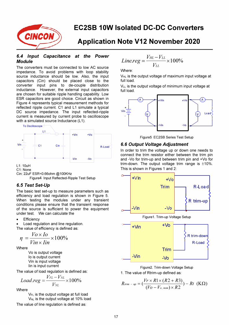
6.4 Input Capacitance at the Power Module
The converters must be connected to low AC source impedance. To avoid problems with loop stability source inductance should be low. Also, the input capacitors (Cin) should be placed close to the converter input pins to de-couple distribution inductance. However, the external input capacitors are chosen for suitable ripple handling capability. Low ESR capacitors are good choice. Circuit as shown in Figure 4 represents typical measurement methods for reflected ripple current. C1 and L1 simulate a typical DC source impedance. The input reflected-ripple current is measured by current probe to oscilloscope with a simulated source Inductance (L1).
C1 Cin
L1
To Oscilloscope
+Vin
-Vin
+Vo
-Vo
R-LoadVin
+
-
L1: 10uH C1: None Cin: 22uF ESR<0.66ohm @100KHz
Figure4 Input Reflected-Ripple Test Setup
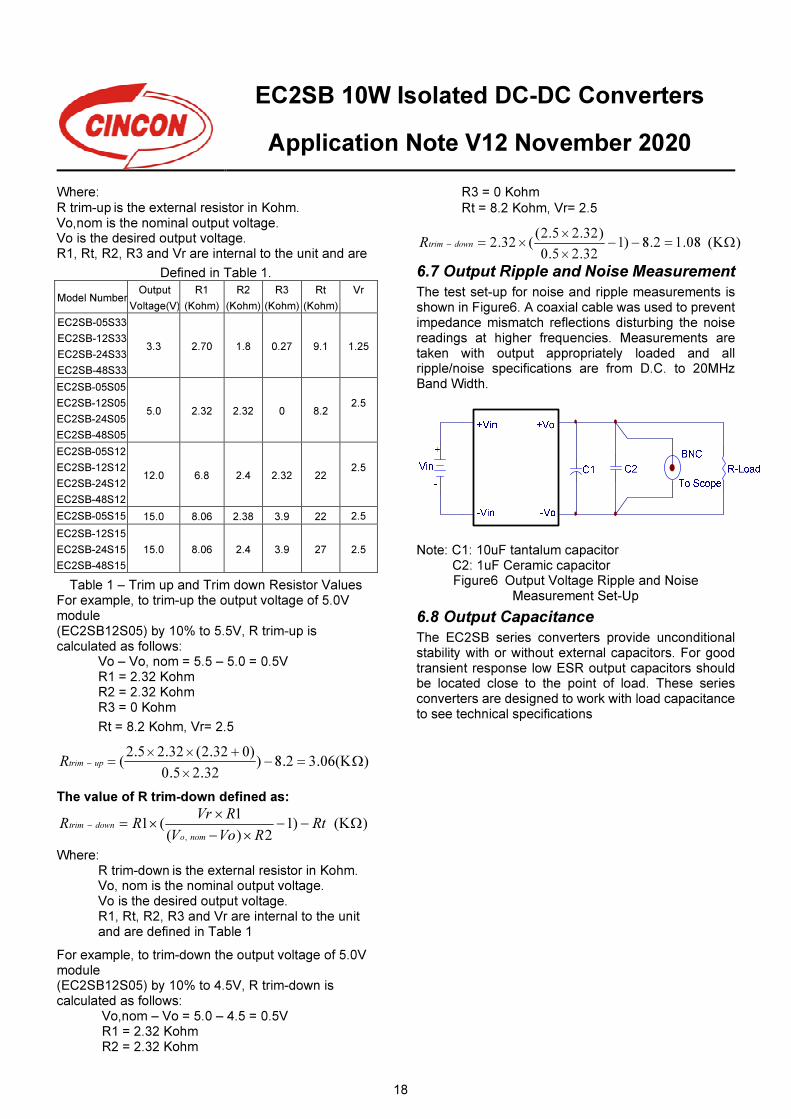
6.5 Test Set-Up
The basic test set-up to measure parameters such as efficiency and load regulation is shown in Figure 5. When testing the modules under any transient conditions please ensure that the transient response of the source is sufficient to power the equipment under test. We can calculate the
• Efficiency • Load regulation and line regulation.
The value of efficiency is defined as:
%100×
×
×
=
IinVin
IoVoη
Where Vo is output voltage Io is output current Vin is input voltage Iin is input current
The value of load regulation is defined as:
%100. ×
−
=
NL
NLFL
V
VVregLoad
Where VFL is the output voltage at full load VNL is the output voltage at 10% load
The value of line regulation is defined as:
%100. ×
−
=
LL
LLHL
V
VVregLine
Where:
VHL is the output voltage of maximum input voltage at full load.
VLL is the output voltage of minimum input voltage at full load.
Figure5 EC2SB Series Test Setup
6.6 Output Voltage Adjustment
In order to trim the voltage up or down one needs to connect the trim resistor either between the trim pin and -Vo for trim-up and between trim pin and +Vo for trim-down. The output voltage trim range is ±10%.
This is shown in Figures 1 and 2:
Figure1. Trim-up Voltage Setup
+Vin
-Vin -Vo
+Vo
R trim-down
R-Load
Trim
Figure2. Trim-down Voltage Setup
1. The value of Rtrim-up defined as:
)(K )2)(
)32(1(
,
Ω−×−
+××=− Rt
RVVo
RRRVrR
nomo
uptrim
EC2SB 10W Isolated DC-DC Converters
Application Note V12 November 2020
18
Where: R trim-up is the external resistor in Kohm. Vo,nom is the nominal output voltage. Vo is the desired output voltage. R1, Rt, R2, R3 and Vr are internal to the unit and are
Defined in Table 1.
Model Number Output
Voltage(V)
R1
(Kohm)
R2
(Kohm)
R3
(Kohm)
Rt
(Kohm)
Vr
EC2SB-05S33
EC2SB-12S33
EC2SB-24S33
EC2SB-48S33
3.3 2.70 1.8 0.27 9.1 1.25
EC2SB-05S05
EC2SB-12S05
EC2SB-24S05
EC2SB-48S05
5.0 2.32 2.32 0 8.2
2.5
EC2SB-05S12
EC2SB-12S12
EC2SB-24S12
EC2SB-48S12
12.0 6.8 2.4 2.32 22
2.5
EC2SB-05S15 15.0 8.06 2.38 3.9 22 2.5
EC2SB-12S15
EC2SB-24S15
EC2SB-48S15
15.0 8.06 2.4 3.9 27 2.5
Table 1 – Trim up and Trim down Resistor Values For example, to trim-up the output voltage of 5.0V module (EC2SB12S05) by 10% to 5.5V, R trim-up is calculated as follows:
Vo – Vo, nom = 5.5 – 5.0 = 0.5V R1 = 2.32 Kohm R2 = 2.32 Kohm R3 = 0 Kohm
Rt = 8.2 Kohm, Vr= 2.5
)06(K.32.8)32.25.0
)032.2(32.25.2( Ω=−
×
+××=− uptrimR
The value of R trim-down defined as:
)(K )12)(
1(1
,
Ω−−×−
××=− Rt
RVoV
RVrRR
nomo
downtrim
Where: R trim-down is the external resistor in Kohm. Vo, nom is the nominal output voltage. Vo is the desired output voltage. R1, Rt, R2, R3 and Vr are internal to the unit and are defined in Table 1
For example, to trim-down the output voltage of 5.0V module (EC2SB12S05) by 10% to 4.5V, R trim-down is calculated as follows:
Vo,nom – Vo = 5.0 – 4.5 = 0.5V R1 = 2.32 Kohm R2 = 2.32 Kohm
R3 = 0 Kohm
Rt = 8.2 Kohm, Vr= 2.5
)(K 08.12.8)132.25.0
)32.25.2((32.2 Ω=−−
×
××=− downtrimR
6.7 Output Ripple and Noise Measurement
The test set-up for noise and ripple measurements is shown in Figure6. A coaxial cable was used to prevent impedance mismatch reflections disturbing the noise readings at higher frequencies. Measurements are taken with output appropriately loaded and all ripple/noise specifications are from D.C. to 20MHz Band Width.
Note: C1: 10uF tantalum capacitor C2: 1uF Ceramic capacitor Figure6 Output Voltage Ripple and Noise
Measurement Set-Up
6.8 Output Capacitance
The EC2SB series converters provide unconditional stability with or without external capacitors. For good transient response low ESR output capacitors should be located close to the point of load. These series converters are designed to work with load capacitance to see technical specifications

EC2SB 10W Isolated DC-DC Converters
Application Note V12 November 2020
19
7. Safety & EMC
7.1 Input Fusing and Safety Considerations.
The EC2SB series converters have not an internal fuse. However, to achieve maximum safety and system protection, always use an input line fuse. We recommended a fast acting fuse, 5A for 5Vin, 4A for 12Vin models, 2A for 24Vin models, 1A 48Vin modules. Figure 7 circuit is recommended by a Transient Voltage Suppressor diode
across the input terminal to protect the unit against surge or spike voltage and input reverse voltage.
+Vin
-Vin
+Vo
-Vo
R-LoadVin
+
-
FUSE
TVS
Figure7 Input Protection
7.2 EMC Considerations
EMI Test standard: EN55032 Class A and Class B Conducted Emission Test Condition: Input Voltage: Nominal, Output Load: Full Load
Figure 8 Connection circuit for conducted EMI testing

EC2SB 10W Isolated DC-DC Converters
Application Note V12 November 2020
20
EN55032 Class A EN55032 Class B
Model No. C1 L1 C1 L1
EC2SB-05S33 NC Short TBD TBD
EC2SB-05S05 NC Short TBD TBD
EC2SB-05S12 NC Short TBD TBD
EC2SB-05S15 NC Short TBD TBD
EC2SB-05D05 NC Short TBD TBD
EC2SB-05D12 NC Short TBD TBD
EC2SB-05D15 NC Short TBD TBD
EC2SB-12S33 NC Short 1uF /100V 1812 3.9uH
EC2SB-12S05 NC Short 1uF /100V 1812 3.9uH
EC2SB-12S12 NC Short 1uF /100V 1812 3.9uH
EC2SB-12S15 NC Short 1uF /100V 1812 3.9uH
EC2SB-12D05 NC Short 1uF /100V 1812 3.9uH
EC2SB-12D12 NC Short 1uF /100V 1812 3.9uH
EC2SB-12D15 NC Short 1uF /100V 1812 3.9uH
EC2SB-24S33 NC Short 1uF /100V 1812 3.9uH
EC2SB-24S05 NC Short 1uF /100V 1812 3.9uH
EC2SB-24S12 NC Short 1uF /100V 1812 3.9uH
EC2SB-24S15 NC Short 1uF /100V 1812 3.9uH
EC2SB-24D05 NC Short 1uF /100V 1812 3.9uH
EC2SB-24D12 NC Short 1uF /100V 1812 3.9uH
EC2SB-24D15 NC Short 1uF /100V 1812 3.9uH
EC2SB-48S33 NC Short 1uF /100V 1812 3.9uH
EC2SB-48S05 NC Short 1uF /100V 1812 3.9uH
EC2SB-48S12 NC Short 1uF /100V 1812 3.9uH
EC2SB-48S15 NC Short 1uF /100V 1812 3.9uH
EC2SB-48D05 NC Short 1uF /100V 1812 3.9uH
EC2SB-48D12 NC Short 1uF /100V 1812 3.9uH
EC2SB48D15 NC Short 1uF /100V 1812 3.9uH
Note: All of capacitors are ceramic capacitors.

EC2SB 10W Isolated DC-DC Converters
Application Note V12 November 2020
21
Figure 9 Conducted Class A of EC2SB-05S33
Figure 10 Conducted Class A of EC2SB-05S05
Figure 11 Conducted Class A of EC2SB-05S12
Figure 12 Conducted Class A of EC2SB-05S15
Figure 13 Conducted Class A of EC2SB-05D05
Figure14 Conducted Class A of EC2SB-05D12
Figure 15 Conducted Class A of EC2SB-05D15
Figure 16 Conducted Class A of EC2SB-12S33
EC2SB 10W Isolated DC-DC Converters
Application Note V12 November 2020
22
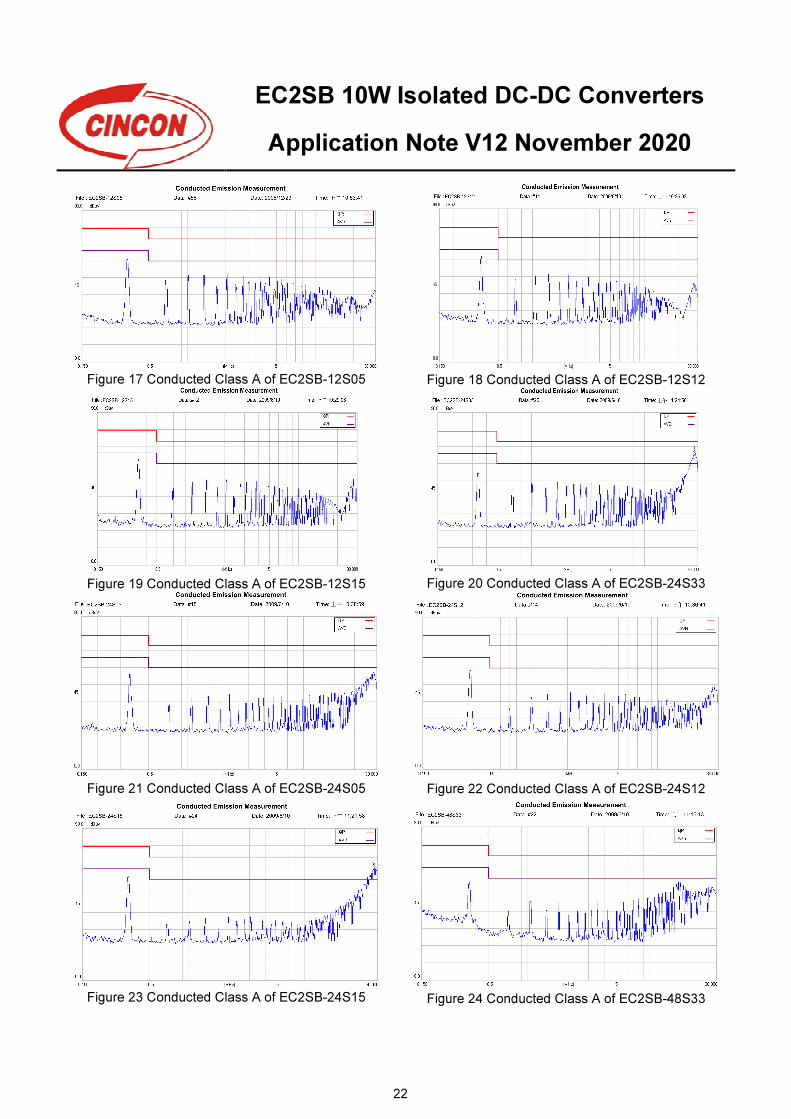
Figure 17 Conducted Class A of EC2SB-12S05
Figure 18 Conducted Class A of EC2SB-12S12
Figure 19 Conducted Class A of EC2SB-12S15
Figure 20 Conducted Class A of EC2SB-24S33
Figure 21 Conducted Class A of EC2SB-24S05
Figure 22 Conducted Class A of EC2SB-24S12
Figure 23 Conducted Class A of EC2SB-24S15
Figure 24 Conducted Class A of EC2SB-48S33

EC2SB 10W Isolated DC-DC Converters
Application Note V12 November 2020
23
Figure 25 Conducted Class A of EC2SB-48S05
Figure 26 Conducted Class A of EC2SB-48S12
Figure 27 Conducted Class A of EC2SB-48S15
Figure 28 Conducted Class B of EC2SB-12S33
Figure 29 Conducted Class B of EC2SB-12S05
Figure 30 Conducted Class B of EC2SB-12S12
Figure 31 Conducted Class B of EC2SB-12S15
Figure 32 Conducted Class B of EC2SB-24S33

EC2SB 10W Isolated DC-DC Converters
Application Note V12 November 2020
24
Figure 33 Conducted Class B of EC2SB-24S05
Figure 34 Conducted Class B of EC2SB-24S12
Figure 35 Conducted Class B of EC2SB-24S15
Figure 36 Conducted Class B of EC2SB-48S33
Figure 37 Conducted Class B of EC2SB-48S05
Figure 38 Conducted Class B of EC2SB-48S12
Figure 38 Conducted Class B of EC2SB-48S15
EC2SB 10W Isolated DC-DC Converters
Application Note V12 November 2020
25
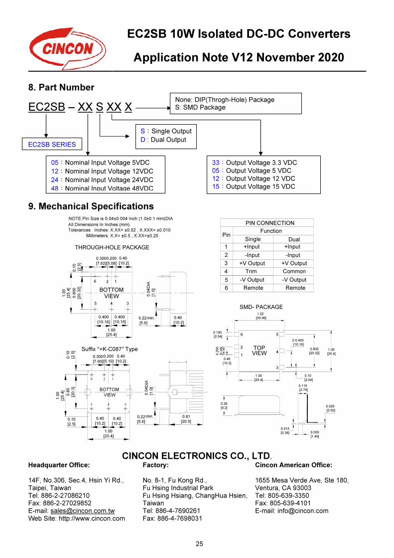
8. Part Number
EC2SB – XX S XX X
9. Mechanical Specifications
BOTTOMVIEW
12
5 4 3
PIN CONNECTION
Pin
1
2
3
4
5
+Input
-Input
+V Output
Trim
-V Output
Function
1.0
0[2
5.4
]
1.00[25.4]
0.1
0
[2.5
]
0.8
00
[20.3
2]
0.400
[10.16]
0.400
[10.16]
0.40
[10.2]
0.200
[5.08]
0.40
[10.2]0.22
[5.6]
0.0
4
[1.0
]
min.
Tolerances Inches: X.XX= ±0.02 , X.XXX= ±0.010
Millimeters: X.X= ±0.5 , X.XX=±0.25
All Dimensions In Inches (mm)
6
0.300
[7.62]
6 Remote
TOPVIEW
0.100
[2.54]
0.200
[5.08]
0.40
[10.2]
1.00
[25.4]
1.00
[25.4]
0.800
[20.32]1
2
6
3
4
5
2-0.400
[10.16]
0.015
[0.38] 0.055
[1.40]
0.110
[2.79]
0.020
[0.50]
1.22
[30.99]
0.10
[2.54]
0.36
[9.2]
Single Dual
+Input
-Input
+V Output
Common
-V Output
Remote
THROUGH-HOLE PACKAGE
SMD- PACKAGE
NOTE:Pin Size is 0.04±0.004 Inch (1.0±0.1 mm)DIA
DIA
0.300
[7.60]
0.200
[5.10]
1.00
[25.4]
1.0
0
[25
.4]
0.8
0
[20
.3]
0.1
0
[2.5
]
0.40
[10.2]
0.40
[10.2]
0.40
[10.2]0.10
[2.5]
BOTTOM
VIEW
345
6 2 1
0.0
4
[1.0
]
0.81
[20.5]
Suffix "+K-C087" Type
DIA
0.22
[5.6]
min.
CINCON ELECTRONICS CO., LTD.
Headquarter Office: 14F, No.306, Sec.4, Hsin Yi Rd., Taipei, Taiwan Tel: 886-2-27086210 Fax: 886-2-27029852 E-mail: [email protected] Web Site: http://www.cincon.com
Factory: No. 8-1, Fu Kong Rd., Fu Hsing Industrial Park Fu Hsing Hsiang, ChangHua Hsien, Taiwan Tel: 886-4-7690261 Fax: 886-4-7698031
Cincon American Office: 1655 Mesa Verde Ave, Ste 180, Ventura, CA 93003 Tel: 805-639-3350 Fax: 805-639-4101 E-mail: [email protected]
EC2SB SERIES
05:Nominal Input Voltage 5VDC
12:Nominal Input Voltage 12VDC
24:Nominal Input Voltage 24VDC
48:Nominal Input Voltage 48VDC
S:Single Output
D : Dual Output
33:Output Voltage 3.3 VDC
05:Output Voltage 5 VDC
12:Output Voltage 12 VDC
15:Output Voltage 15 VDC
None: DIP(Throgh-Hole) Package S: SMD Package