Embed Size (px)
DESCRIPTION
Lab Manual;ECE;Third Year,Anna University
Citation preview

EINSTEIN COLLEGE OF ENGINEERING Sir.C.V.Raman Nagar, Tirunelveli-12
Department of Electronics and Communication Engineering
Subject Code :EC 58
“Microprocessors and Microcontrollers Lab”
Name : ……………………………………
Reg No : ……………………………………
Branch : ……………………………………
Year & Semester : ……………………………………
Sub Code: EC 58 Microprocessors and Microcontrollers Lab
©Einstein College of Engineering
Page 2 of 76
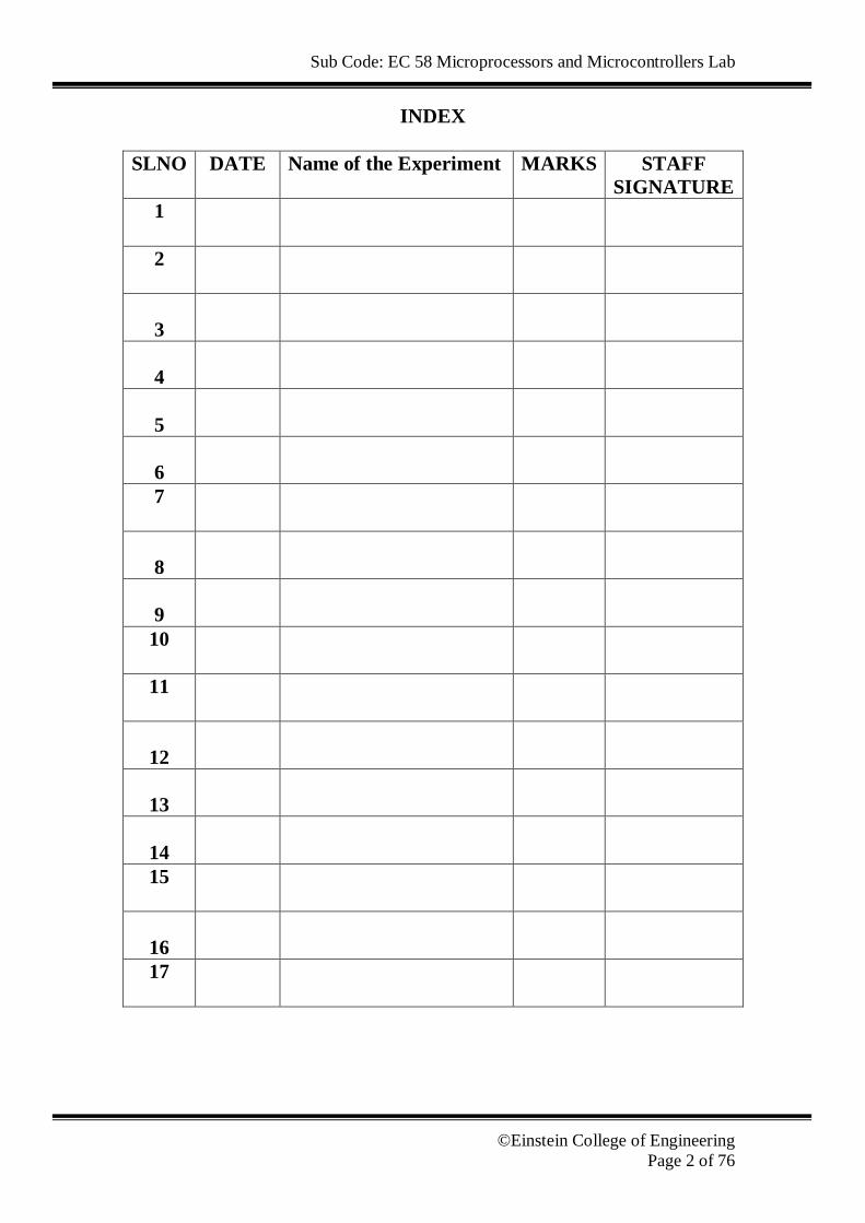
INDEX
SLNO DATE Name of the Experiment MARKS STAFF SIGNATURE
1
2
3
4
5
6
7
8
9
10
11
12
13
14
15
16
17

Sub Code: EC 58 Microprocessors and Microcontrollers Lab
©Einstein College of Engineering
Page 3 of 76
EX.NO. :1 DATE :
8-BIT ARITHMETIC OPERATIONS
8-BIT ADDITION: AIM To write an ALP to perform 8-bit addition using 8085 microprocessor trainer kit. APPARATUS REQUIRED
1. 8085 microprocessor trainer kit. 2. Power supply
ALGORITHM
1. Start the program 2. Get the first data to the accumulator. 3. The second data is given to B register. 4. The content of B register is then added with accumulator contents. 5. The addition for carry is checked and the result is stored in the specified memory location 6. The program is terminated.
PROGRAM
ADDRESS
LABEL
MNEMONICS
OPCODE
4100 4102 4104 4105 4108 410A 410D 410E 410F 4112
START L1
MVI A, 35 MVI B, 12 ADD B STA 4200 MVI C, 00 JNC L1 INR C MOV A, C STA 4201 HLT
3E,35 06,12 80 32,00,42 0E,00 D2,0E,41 0C 79 32,01,42 76

Sub Code: EC 58 Microprocessors and Microcontrollers Lab
©Einstein College of Engineering
Page 4 of 76
INPUT: 4101-35 4103-12 OUTPUT: 4200-47 4201-00 MANUAL CALCULATION:
Sub Code: EC 58 Microprocessors and Microcontrollers Lab
©Einstein College of Engineering
Page 5 of 76
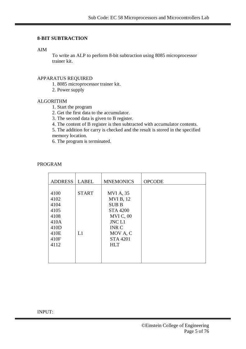
8-BIT SUBTRACTION AIM
To write an ALP to perform 8-bit subtraction using 8085 microprocessor trainer kit.
APPARATUS REQUIRED
1. 8085 microprocessor trainer kit. 2. Power supply
ALGORITHM
1. Start the program 2. Get the first data to the accumulator. 3. The second data is given to B register. 4. The content of B register is then subtracted with accumulator contents. 5. The addition for carry is checked and the result is stored in the specified memory location. 6. The program is terminated.
PROGRAM
ADDRESS
LABEL
MNEMONICS
OPCODE
4100 4102 4104 4105 4108 410A 410D 410E 410F 4112
START L1
MVI A, 35 MVI B, 12 SUB B STA 4200 MVI C, 00 JNC L1 INR C MOV A, C STA 4201 HLT
INPUT:

Sub Code: EC 58 Microprocessors and Microcontrollers Lab
©Einstein College of Engineering
Page 6 of 76
4101-35 4103-12 OUTPUT: 4200-23 4201-00 MANUAL CALCULATION:

Sub Code: EC 58 Microprocessors and Microcontrollers Lab
©Einstein College of Engineering
Page 7 of 76
8-BIT MULTIPLICATION AIM
To write an ALP to perform 8-bit multiplication using 8085 microprocessor trainer kit.
APPARATUS REQUIRED
1. 8085 microprocessor trainer kit. 2. Power supply
ALGORITHM
1. Start the program 2. Clear the accumulator 3. Get the first data to the register B. 4. Get the second data to the register C. 5. Add the contents of register B is added with the accumulator and stored in accumulator. 6. After performing the addition operation the register C would decremented by 1 7. When the zero flag is set, the result was stored in the specified memory location. 8. Otherwise the loop of addition operation was continued.
PROGRAM
ADDRESS
LABEL
MNEMONICS
OPCODE
4100 4102 4104 4106 4107 4108 410B 410E
START L1
MVI A, 00 MVI B, 12 MVI C, 45 ADD B DCR C JNZ L1 STA 4200 HLT

Sub Code: EC 58 Microprocessors and Microcontrollers Lab
©Einstein College of Engineering
Page 8 of 76
INPUT: 4103-12 4105-45 OUTPUT: 4200- MANUAL CALCULATION
Sub Code: EC 58 Microprocessors and Microcontrollers Lab
©Einstein College of Engineering
Page 9 of 76
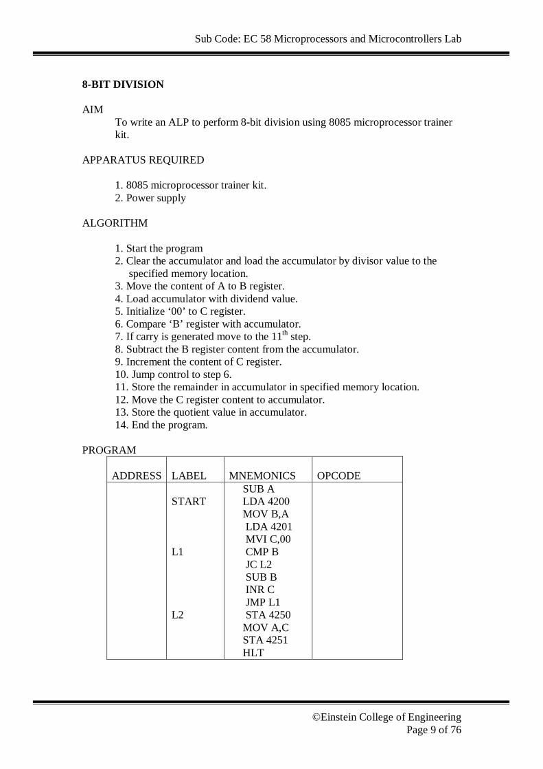
8-BIT DIVISION AIM
To write an ALP to perform 8-bit division using 8085 microprocessor trainer kit.
APPARATUS REQUIRED
1. 8085 microprocessor trainer kit. 2. Power supply
ALGORITHM
1. Start the program 2. Clear the accumulator and load the accumulator by divisor value to the specified memory location. 3. Move the content of A to B register. 4. Load accumulator with dividend value. 5. Initialize ‘00’ to C register. 6. Compare ‘B’ register with accumulator. 7. If carry is generated move to the 11th step. 8. Subtract the B register content from the accumulator. 9. Increment the content of C register. 10. Jump control to step 6. 11. Store the remainder in accumulator in specified memory location. 12. Move the C register content to accumulator. 13. Store the quotient value in accumulator. 14. End the program.
PROGRAM
ADDRESS
LABEL
MNEMONICS
OPCODE
START L1 L2
SUB A LDA 4200 MOV B,A LDA 4201 MVI C,00 CMP B JC L2 SUB B INR C JMP L1 STA 4250 MOV A,C STA 4251 HLT

Sub Code: EC 58 Microprocessors and Microcontrollers Lab
©Einstein College of Engineering
Page 10 of 76
INPUT: OUTPUT: MANUAL CALCULATION: RESULT:
Thus the ALP was written and the 8 bit arithmetic operations were performed successfully using 8085 microprocessor trainer kit.
EX.NO. :2
Sub Code: EC 58 Microprocessors and Microcontrollers Lab
©Einstein College of Engineering
Page 11 of 76
DATE : 16-BIT ARITHMETIC OPERATIONS
16-BIT ADDITION AIM
To write an ALP to perform 16-bit addition using 8086 microprocessor trainer kit.
APPARATUS REQUIRED
1. 8085 microprocessor trainer kit. 2.Power supply
ALGORITHM
.
PROGRAM
Sub Code: EC 58 Microprocessors and Microcontrollers Lab
©Einstein College of Engineering
Page 12 of 76
INPUT: OUTPUT: MANUAL CALCULATION:

Sub Code: EC 58 Microprocessors and Microcontrollers Lab
©Einstein College of Engineering
Page 13 of 76

Sub Code: EC 58 Microprocessors and Microcontrollers Lab
©Einstein College of Engineering
Page 14 of 76
Sub Code: EC 58 Microprocessors and Microcontrollers Lab
©Einstein College of Engineering
Page 15 of 76
RESULT:
Thus the ALP was written and the 16-bit arithmetic operations was performed successfully by using the 8086 microprocessor trainer
Sub Code: EC 58 Microprocessors and Microcontrollers Lab
©Einstein College of Engineering
Page 16 of 76
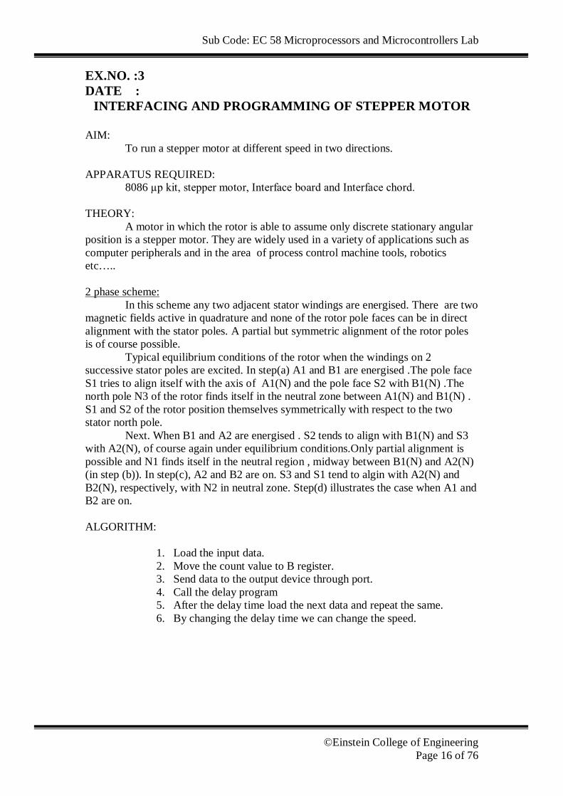
EX.NO. :3 DATE :
INTERFACING AND PROGRAMMING OF STEPPER MOTOR AIM: To run a stepper motor at different speed in two directions. APPARATUS REQUIRED: 8086 µp kit, stepper motor, Interface board and Interface chord. THEORY: A motor in which the rotor is able to assume only discrete stationary angular position is a stepper motor. They are widely used in a variety of applications such as computer peripherals and in the area of process control machine tools, robotics etc….. 2 phase scheme: In this scheme any two adjacent stator windings are energised. There are two magnetic fields active in quadrature and none of the rotor pole faces can be in direct alignment with the stator poles. A partial but symmetric alignment of the rotor poles is of course possible. Typical equilibrium conditions of the rotor when the windings on 2 successive stator poles are excited. In step(a) A1 and B1 are energised .The pole face S1 tries to align itself with the axis of A1(N) and the pole face S2 with B1(N) .The north pole N3 of the rotor finds itself in the neutral zone between A1(N) and B1(N) . S1 and S2 of the rotor position themselves symmetrically with respect to the two stator north pole. Next. When B1 and A2 are energised . S2 tends to align with B1(N) and S3 with A2(N), of course again under equilibrium conditions.Only partial alignment is possible and N1 finds itself in the neutral region , midway between B1(N) and A2(N) (in step (b)). In step(c), A2 and B2 are on. S3 and S1 tend to algin with A2(N) and B2(N), respectively, with N2 in neutral zone. Step(d) illustrates the case when A1 and B2 are on. ALGORITHM:
1. Load the input data. 2. Move the count value to B register. 3. Send data to the output device through port. 4. Call the delay program 5. After the delay time load the next data and repeat the same. 6. By changing the delay time we can change the speed.

Sub Code: EC 58 Microprocessors and Microcontrollers Lab
©Einstein College of Engineering
Page 17 of 76

Sub Code: EC 58 Microprocessors and Microcontrollers Lab
©Einstein College of Engineering
Page 18 of 76
Sub Code: EC 58 Microprocessors and Microcontrollers Lab
©Einstein College of Engineering
Page 19 of 76
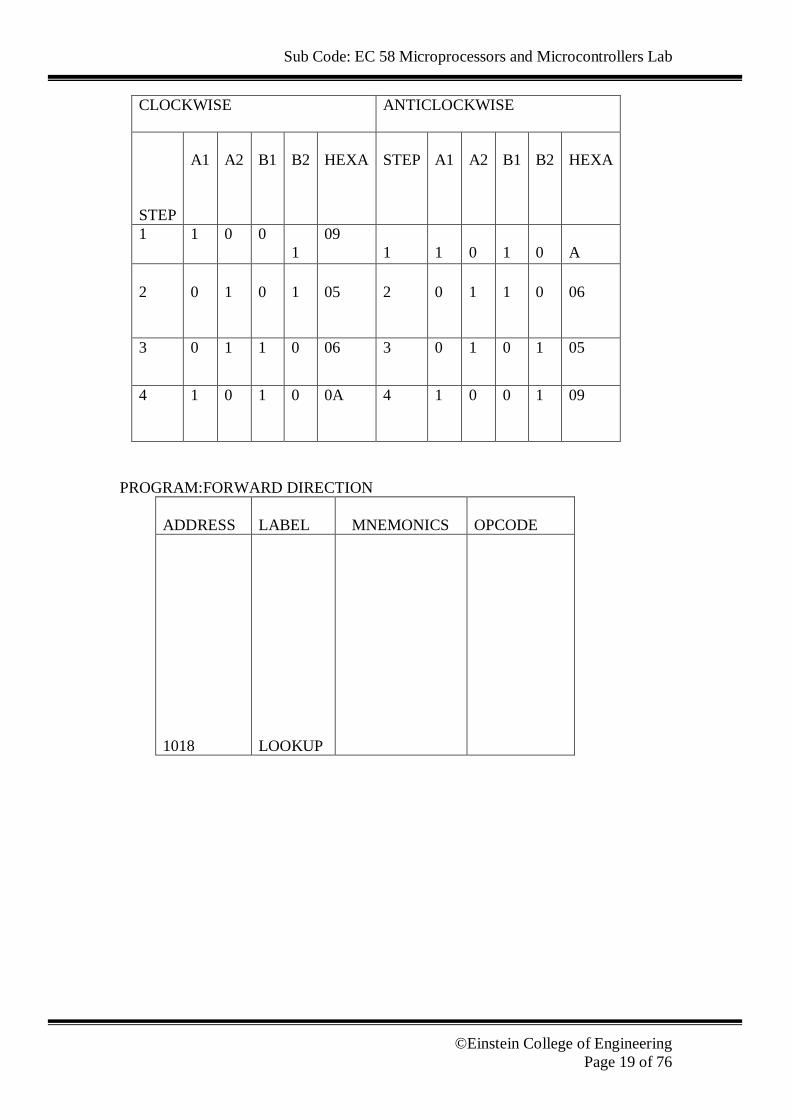
CLOCKWISE ANTICLOCKWISE
STEP
A1
A2
B1
B2
HEXA
STEP
A1
A2
B1
B2
HEXA
1
1
0
0
1
09
1
1
0
1
0
A
2
0
1
0
1
05
2
0
1
1
0
06
3 0 1 1 0 06 3 0 1 0 1 05
4 1 0 1 0 0A 4 1 0 0 1 09
PROGRAM:FORWARD DIRECTION
ADDRESS
LABEL
MNEMONICS
OPCODE
1018
LOOKUP

Sub Code: EC 58 Microprocessors and Microcontrollers Lab
©Einstein College of Engineering
Page 20 of 76
REVERSE DIRECTION
ADDRESS
LABEL
MNEMONICS
OPCODE
RESULT: Thus a program to run a stepper motor at different speeds in two directions was written and executed using 8086 µp

Sub Code: EC 58 Microprocessors and Microcontrollers Lab
©Einstein College of Engineering
Page 21 of 76
EX.NO. :4 DATE :
ANALOG TO DIGITAL CONVERTER
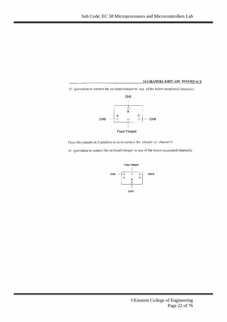
AIM: To write an assembly language program to convert analog to digital output APPARATUS REQUIRED: 8085 µp kit, ADC board, Interface chord, Power chord. ALGORITHM: 1. Load the data 10 H to make the ALE signal low. 2. Load the data 18 H to make the ALE signal low. 3. Place jumper J2 in B position. 4. Place jumper J5 in A position. 5. Enter & execute the program. 6. Vary the analog input (using prompt) and give the SOC (by pressing the SOC switch). 7. Set the corresponding digital value in the LED display. THEORY: The device contains an 8 channel single ended analog signal multiplexer. A particular input channel is selected by using the address decoding.
I/O decoding A 3:8 decoder 74LS138 is employed to generate I/O decoding logic. The address lines A3, A4, and A5 are tied to pin 1, 2, 3 of 74LS138 respectively. The address lines A6 and A7 are NANDed together and the NAND gate o/p is connected to pin 5 of 74LS 138.similarly IOW and IOR signals NANDed together and the NAND gate o/p is connected to pin 6 of 74LS 138. Pin 4 is grounded. The buffer 74LS244 which transfers the converted data output to data bus is selected when A7 A6 A5 A4 A3 A2 A1 A0 1 1 0 0 0 X X X =C0 H
Sub Code: EC 58 Microprocessors and Microcontrollers Lab
©Einstein College of Engineering
Page 22 of 76

Sub Code: EC 58 Microprocessors and Microcontrollers Lab
©Einstein College of Engineering
Page 23 of 76
Sub Code: EC 58 Microprocessors and Microcontrollers Lab
©Einstein College of Engineering
Page 24 of 76
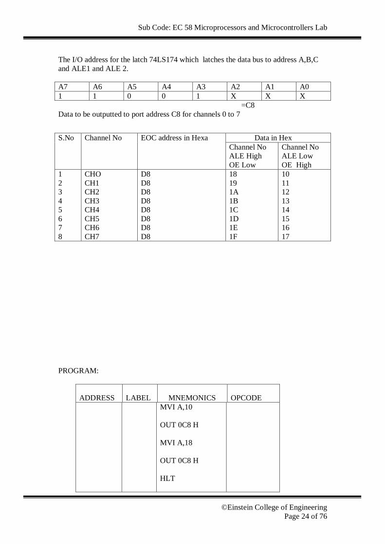
The I/O address for the latch 74LS174 which latches the data bus to address A,B,C and ALE1 and ALE 2. A7 A6 A5 A4 A3 A2 A1 A0 1 1 0 0 1 X X X =C8 Data to be outputted to port address C8 for channels 0 to 7
PROGRAM:
ADDRESS
LABEL
MNEMONICS
OPCODE
MVI A,10 OUT 0C8 H MVI A,18 OUT 0C8 H HLT
S.No Channel No
EOC address in Hexa Data in Hex Channel No ALE High OE Low
Channel No ALE Low OE High
1 2 3 4 5 6 7 8
CHO CH1 CH2 CH3 CH4 CH5 CH6 CH7
D8 D8 D8 D8 D8 D8 D8 D8
18 19 1A 1B 1C 1D 1E 1F
10 11 12 13 14 15 16 17

Sub Code: EC 58 Microprocessors and Microcontrollers Lab
©Einstein College of Engineering
Page 25 of 76
MANUAL CALCULATION RESULT: Thus the assembly language program to convert analog to digital output digital output was executed successfully.

Sub Code: EC 58 Microprocessors and Microcontrollers Lab
©Einstein College of Engineering
Page 26 of 76
EX.NO. :5 DATE :
GENRATION OF SIMPLE WAVEFORMS USING DAC
AIM To generate square, sawtooth, triangular and sine waveforms using DAC. APPARATUS REQUIRED: 8085 µp kit, CRO, DAC and interfacing chords. CIRCUIT IMPLEMENTATION: The basic DAC interface board incorporates two 8 bit digital to analog converters, DAC0800.The DAC interface section comprises of I/O decoding and D/A conversion circuit.
I/O decoding
A 3:8 decoder 74LS138 is employed to generate I/O decoding logic. The address lines A3, A4, and A5 are tied to pin 1, 2, 3 of 74LS138 respectively. The address lines A6 and A7 are NANDed together and the NAND gate o/p is connected to pin 5 of 74LS 138.similarly IOW and IOR signals NANDed together and the NAND gate o/p is connected to pin 6 of 74LS 138. Pin 4 is grounded. Thus with A7 A6 A5 A4 A3 A2 A1 A0 1 1 0 0 0 X X X =C0 H DAC1 is selected, and with A7 A6 A5 A4 A3 A2 A1 A0 1 1 0 0 1 X X X =C8 DAC2 is selected
Sub Code: EC 58 Microprocessors and Microcontrollers Lab
©Einstein College of Engineering
Page 27 of 76
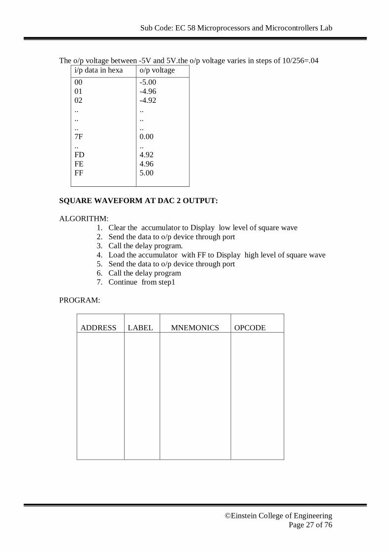
The o/p voltage between -5V and 5V.the o/p voltage varies in steps of 10/256=.04
i/p data in hexa o/p voltage 00 01 02 .. .. .. 7F .. FD FE FF
-5.00 -4.96 -4.92 .. .. .. 0.00 .. 4.92 4.96 5.00
SQUARE WAVEFORM AT DAC 2 OUTPUT: ALGORITHM:
1. Clear the accumulator to Display low level of square wave 2. Send the data to o/p device through port 3. Call the delay program. 4. Load the accumulator with FF to Display high level of square wave 5. Send the data to o/p device through port 6. Call the delay program 7. Continue from step1
PROGRAM:
ADDRESS
LABEL
MNEMONICS
OPCODE

Sub Code: EC 58 Microprocessors and Microcontrollers Lab
©Einstein College of Engineering
Page 28 of 76
OUTPUT: SAWTOOTH WAVEFORM AT DAC 1 OUTPUT: ALGORITHM :
1. Clear the accumulator 2. Send the data to o/p device through port 3. Incrément the accumulator to display next o/p voltage. 4. Do the above process until zero flag is set 5. Continue from step1
PROGRAM:
ADDRESS
LABEL
MNEMONICS
OPCODE
OUTPUT: TRIANGULAR WAVEFORM AT DAC2OUTPUT: ALGORITHM:
1. Clear the accumulator through L register. 2. Send the data to o/p device through port 3. Incrément the L register 4. Do the above process until zero flag is set 5. Load the accumulator with FF through L register.
Sub Code: EC 58 Microprocessors and Microcontrollers Lab
©Einstein College of Engineering
Page 29 of 76
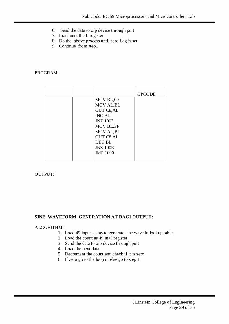
6. Send the data to o/p device through port 7. Incrément the L register 8. Do the above process until zero flag is set 9. Continue from step1
PROGRAM:
OPCODE
MOV BL,00 MOV AL,BL OUT C8,AL INC BL JNZ 1003 MOV BL,FF MOV AL,BL OUT C8,AL DEC BL JNZ 100E JMP 1000
OUTPUT: SINE WAVEFORM GENERATION AT DAC1 OUTPUT: ALGORITHM:
1. Load 49 input datas to generate sine wave in lookup table 2. Load the count as 49 in C register 3. Send the data to o/p device through port 4. Load the next data 5. Decrement the count and check if it is zero 6. If zero go to the loop or else go to step 1

Sub Code: EC 58 Microprocessors and Microcontrollers Lab
©Einstein College of Engineering
Page 30 of 76
FORMULA USED: 128+128 SINX° WHERE X=0 to 360 with step 5 EXAMPLE:
DEGREES
DECIMAL
HEXA
0
128
80
PROGRAM:
ADDRESS
LABEL
MNEMONICS
OPCODE
1100
LOOKUP
MOV BX,1100 MOV CL,49 MOV AL,[BX] OUT C0,AL INC BX LOOP 1007 JMP 1000 80,8B,96,A1,AB,B6, C0,C9,D2,DA,E2,E8, EF,F4,F8,FB,FE,FF, FF,FF,FF,FE,FB,F8, F4,EF,E8,E2,DA,D2, C9,C0,B6,AB,A1,96 ,8B,80,74,6A,5F,54, 4A,40,36,2E,25,1E, 17,11,0C,08,04,02,00, 00,00,02,04,08,0C,11, 17,1E,25,2E,36,40, 4A,54,5F,6A,74,80

Sub Code: EC 58 Microprocessors and Microcontrollers Lab
©Einstein College of Engineering
Page 31 of 76
RESULT: Thus the square, saw tooth, triangular and sine waveforms were generated using 8086 µp.
Sub Code: EC 58 Microprocessors and Microcontrollers Lab
©Einstein College of Engineering
Page 32 of 76
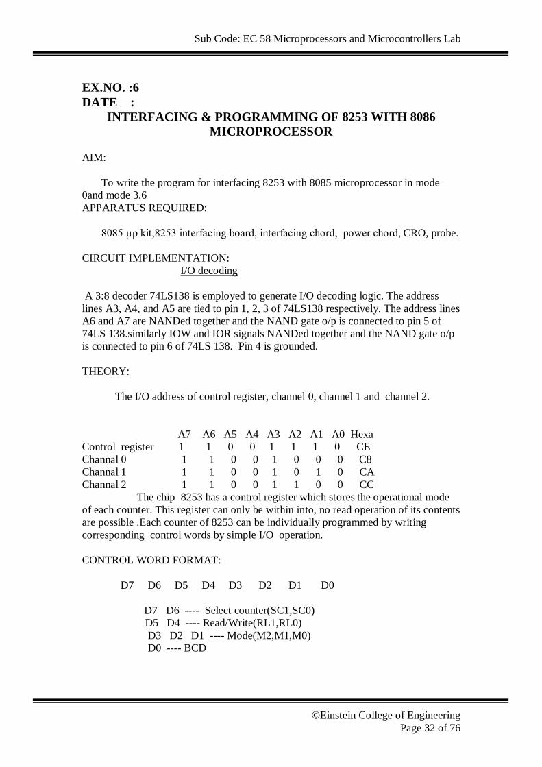
EX.NO. :6 DATE :
INTERFACING & PROGRAMMING OF 8253 WITH 8086 MICROPROCESSOR
AIM: To write the program for interfacing 8253 with 8085 microprocessor in mode 0and mode 3.6 APPARATUS REQUIRED: 8085 µp kit,8253 interfacing board, interfacing chord, power chord, CRO, probe. CIRCUIT IMPLEMENTATION:
I/O decoding A 3:8 decoder 74LS138 is employed to generate I/O decoding logic. The address lines A3, A4, and A5 are tied to pin 1, 2, 3 of 74LS138 respectively. The address lines A6 and A7 are NANDed together and the NAND gate o/p is connected to pin 5 of 74LS 138.similarly IOW and IOR signals NANDed together and the NAND gate o/p is connected to pin 6 of 74LS 138. Pin 4 is grounded. THEORY: The I/O address of control register, channel 0, channel 1 and channel 2. A7 A6 A5 A4 A3 A2 A1 A0 Hexa Control register 1 1 0 0 1 1 1 0 CE Channal 0 1 1 0 0 1 0 0 0 C8 Channal 1 1 1 0 0 1 0 1 0 CA Channal 2 1 1 0 0 1 1 0 0 CC The chip 8253 has a control register which stores the operational mode of each counter. This register can only be within into, no read operation of its contents are possible .Each counter of 8253 can be individually programmed by writing corresponding control words by simple I/O operation. CONTROL WORD FORMAT: D7 D6 D5 D4 D3 D2 D1 D0 D7 D6 ---- Select counter(SC1,SC0) D5 D4 ---- Read/Write(RL1,RL0) D3 D2 D1 ---- Mode(M2,M1,M0) D0 ---- BCD
Sub Code: EC 58 Microprocessors and Microcontrollers Lab
©Einstein College of Engineering
Page 33 of 76
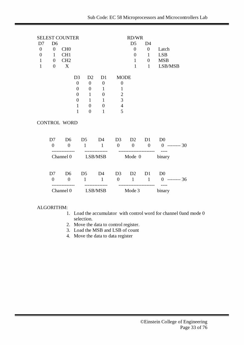
SELEST COUNTER RD/WR D7 D6 D5 D4 0 0 CH0 0 0 Latch 0 1 CH1 0 1 LSB 1 0 CH2 1 0 MSB 1 0 X 1 1 LSB/MSB D3 D2 D1 MODE 0 0 0 0 0 0 1 1 0 1 0 2 0 1 1 3 1 0 0 4 1 0 1 5 CONTROL WORD D7 D6 D5 D4 D3 D2 D1 D0 0 0 1 1 0 0 0 0 -------- 30 -------------- -------------- ---------------------- ---- Channel 0 LSB/MSB Mode 0 binary
D7 D6 D5 D4 D3 D2 D1 D0 0 0 1 1 0 1 1 0 -------- 36 -------------- -------------- ---------------------- ---- Channel 0 LSB/MSB Mode 3 binary
ALGORITHM:
1. Load the accumulator with control word for channel 0and mode 0 selection.
2. Move the data to control register. 3. Load the MSB and LSB of count 4. Move the data to data register

Sub Code: EC 58 Microprocessors and Microcontrollers Lab
©Einstein College of Engineering
Page 34 of 76
OUTPUT: EXAMPLE: CLOCK FREQUENCY=1.5MHZ REQUIRED FREQUENCY=150KHZ COUNT=1.5M/150K=10 (decimal)=0A(hexa) MANUAL CALCULATION: OUTPUT:
Sub Code: EC 58 Microprocessors and Microcontrollers Lab
©Einstein College of Engineering
Page 35 of 76
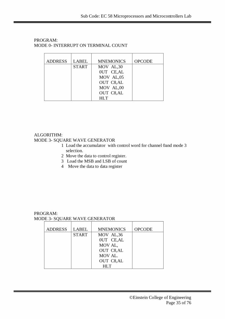
PROGRAM: MODE 0- INTERRUPT ON TERMINAL COUNT
ADDRESS
LABEL
MNEMONICS
OPCODE
START MOV AL,30 0UT CE,AL MOV AL,05 OUT C8,AL MOV AL,00 OUT C8,AL HLT
ALGORITHM: MODE 3- SQUARE WAVE GENERATOR
1 Load the accumulator with control word for channel 0and mode 3 selection. 2 Move the data to control register. 3 Load the MSB and LSB of count 4 Move the data to data register
PROGRAM: MODE 3- SQUARE WAVE GENERATOR
ADDRESS
LABEL
MNEMONICS
OPCODE
START MOV AL,36 0UT CE,AL MOV AL, OUT C8,AL MOV AL. OUT C8,AL HLT
Sub Code: EC 58 Microprocessors and Microcontrollers Lab
©Einstein College of Engineering
Page 36 of 76
RESULT: Thus the program for 8253 interfacing with 8086 microprocessor was
written successfully.
Sub Code: EC 58 Microprocessors and Microcontrollers Lab
©Einstein College of Engineering
Page 37 of 76
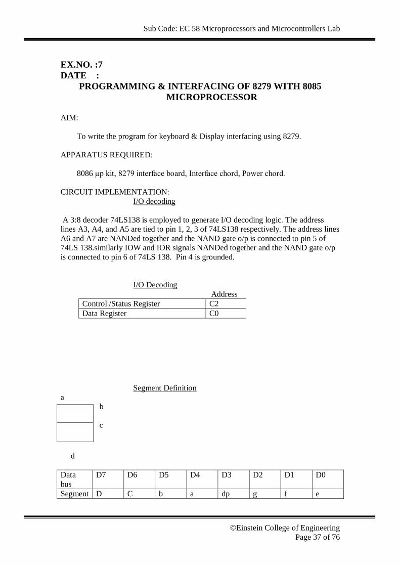
EX.NO. :7 DATE :
PROGRAMMING & INTERFACING OF 8279 WITH 8085 MICROPROCESSOR AIM: To write the program for keyboard & Display interfacing using 8279. APPARATUS REQUIRED: 8086 µp kit, 8279 interface board, Interface chord, Power chord. CIRCUIT IMPLEMENTATION:
I/O decoding A 3:8 decoder 74LS138 is employed to generate I/O decoding logic. The address lines A3, A4, and A5 are tied to pin 1, 2, 3 of 74LS138 respectively. The address lines A6 and A7 are NANDed together and the NAND gate o/p is connected to pin 5 of 74LS 138.similarly IOW and IOR signals NANDed together and the NAND gate o/p is connected to pin 6 of 74LS 138. Pin 4 is grounded. I/O Decoding
Address Control /Status Register C2 Data Register C0
Segment Definition
a b c
d Data bus
D7 D6 D5 D4 D3 D2 D1 D0
Segment D C b a dp g f e
Sub Code: EC 58 Microprocessors and Microcontrollers Lab
©Einstein College of Engineering
Page 38 of 76
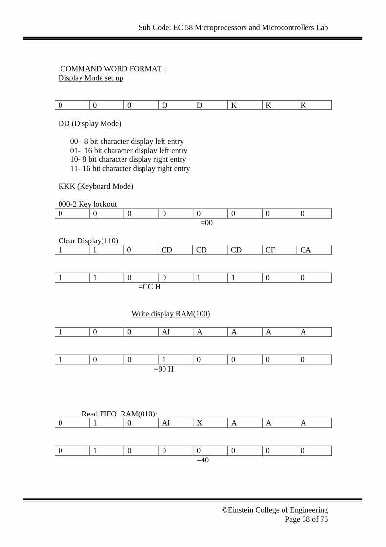
COMMAND WORD FORMAT : Display Mode set up 0 0 0 D D K K K DD (Display Mode)
00- 8 bit character display left entry 01- 16 bit character display left entry 10- 8 bit character display right entry 11- 16 bit character display right entry
KKK (Keyboard Mode) 000-2 Key lockout 0 0 0 0 0 0 0 0 =00 Clear Display(110) 1 1 0 CD CD CD CF CA 1 1 0 0 1 1 0 0
=CC H Write display RAM(100) 1 0 0 AI A A A A 1 0 0 1 0 0 0 0 =90 H
Read FIFO RAM(010): 0 1 0 AI X A A A
0 1 0 0 0 0 0 0 =40

Sub Code: EC 58 Microprocessors and Microcontrollers Lab
©Einstein College of Engineering
Page 39 of 76
Read FIFO Status
DU S/E O U F N N N
0 0 0 0 0 1 1 1 =07 CLEAR DISPLAY RAM
1 1 1 1 1 1 1 1 =FF
(A) KEYBOARD INTERFACE ALGORITHM: 1. Load the data count in B register 2. Set display mode 3. Move the data to control register. 4. Clear display. 5. Move the data to control register. 6. Write display RAM 7. Move the data to control register 8. Clear the display RAM 9. Move the data to data register. 10. Decrement the count 11. Repeat the step5 for all the data display 12. Check whether the key is pressed or not 13. If the key is pressed go to next step otherwise repeat step 12. 14. Set to read FIFO RAM. 15. Move the data to control register 16. Get the data from the pressed key & display it
Sub Code: EC 58 Microprocessors and Microcontrollers Lab
©Einstein College of Engineering
Page 40 of 76
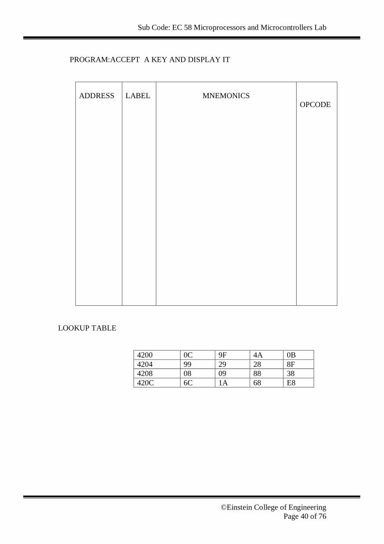
PROGRAM:ACCEPT A KEY AND DISPLAY IT
ADDRESS
LABEL
MNEMONICS
OPCODE
LOOKUP TABLE
4200 0C 9F 4A 0B 4204 99 29 28 8F 4208 08 09 88 38 420C 6C 1A 68 E8

Sub Code: EC 58 Microprocessors and Microcontrollers Lab
©Einstein College of Engineering
Page 41 of 76
(B) (ROLLING DISPLAY) ALGORITHM: 1. Initialise the counter 2. Set Display mode. 3. Move the data to control register 4. Clear display 5. Move the data to control register 6. set the write display RAM 7. Move the data to control register 8. Get the first data to be displayed 9. Display the data 10. Call the delay subroutine 11. Get the next data & repeat the steps 9,10until the count is zero

Sub Code: EC 58 Microprocessors and Microcontrollers Lab
©Einstein College of Engineering
Page 42 of 76
PROGRAM
ADDRESS
LABEL
MNEMONICS
OPCODE
LOOK UP 1200 FF FF FF FF 1204 FF FF FF FF 1208 98 68 7C C8 120C 1C 29 FF FF
Sub Code: EC 58 Microprocessors and Microcontrollers Lab
©Einstein College of Engineering
Page 43 of 76
RESULT: Thus keyboard & Display were interfaced with 8279 by using 8086microprocessor.

Sub Code: EC 58 Microprocessors and Microcontrollers Lab
©Einstein College of Engineering
Page 44 of 76
EX.NO. :8 DATE :
MAXIMUM AND MINIMUM OF NUMBERS
AIM: To write a program for searching largest and smallest numbers in an array using 8086µp. APPARATUS REQUIRED: 8086 µp kit, keyboard, power chord. MINIMUM NUMBER: ALGORITHM:
1. Get the COUNT in CX register and inputs in specified memory location. 2. Compare the 1st two datas and load the small data in accumulator. 3. Compare the accumulator with the remaining datas and store the smallest
data in accumulator. 4. Stop the program.
PROGRAM: ADDRESS
LABEL
MNEMONICS
OPCODE
START L2 L1
MOV DX,05 DEC DX MOV CX,DX MOV BX,1100 MOVAX,[BX] ADD BX,2 CMP AX,[BX] JB L1 MOV AX,[BX] LOOP L2 MOV [1500],AX HLT
Sub Code: EC 58 Microprocessors and Microcontrollers Lab
©Einstein College of Engineering
Page 45 of 76
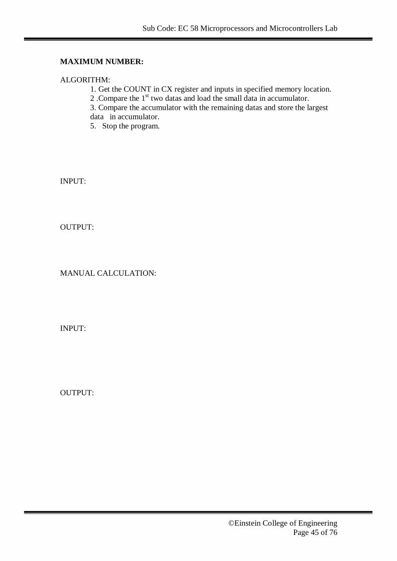
MAXIMUM NUMBER: ALGORITHM:
1. Get the COUNT in CX register and inputs in specified memory location. 2 .Compare the 1st two datas and load the small data in accumulator. 3. Compare the accumulator with the remaining datas and store the largest data in accumulator. 5. Stop the program.
INPUT: OUTPUT: MANUAL CALCULATION:
INPUT: OUTPUT:

Sub Code: EC 58 Microprocessors and Microcontrollers Lab
©Einstein College of Engineering
Page 46 of 76
PROGRAM:
ADDRESS
LABEL
MNEMONICS
OPCODE
START L2 L1
MOV DX,05 DEC DX MOV CX,DX MOV BX,1100 MOVAX,[BX] ADD BX,2 CMP AX,[BX] JNB L1 MOV AX,[BX] LOOP L2 MOV [1500],AX HLT
RESULT: Thus the ALP for searching largest and smallest numbers from an array of datas was executed using 8086µp.

Sub Code: EC 58 Microprocessors and Microcontrollers Lab
©Einstein College of Engineering
Page 47 of 76
EX.NO.:9 DATE :
SORTING AN ARRAY AIM: To write a program to sort an array in ascending and descending order by using 8086 µp. APPARATUS REQUIRED: 8086 µp kit, keyboard, power chord. ASCENDING ORDER: ALGORITHM:
1. Get the number of inputs. 2. Load the inputs in memory location 1100. 3. Compare the 1st and 2nd data. 4. If there is carry go to step 6. 5. If no carry exchange two datas. 6. Compare 2nd and 3rd data and repeat the same up to last data. 7. Now, we get the largest number in the last place. 8. Repeat the steps from 3. 9. Stop the program.
PROGRAM:
ADDRESS
LABEL
MNEMONICS
OPCODE
START L1 L2 L3
MOV CX,05 MOV DX,CX MOV BX,1100 MOV AX,[BX] CMP AX,[BX+2] JB L3 XCHG [BX+2],AX MOV [BX],AX ADD BX,2 LOOP L2 MOV CX,DX LOOP L1 HLT
Sub Code: EC 58 Microprocessors and Microcontrollers Lab
©Einstein College of Engineering
Page 48 of 76
INPUT: OUTPUT: MANUAL CALCULATION:
Sub Code: EC 58 Microprocessors and Microcontrollers Lab
©Einstein College of Engineering
Page 49 of 76
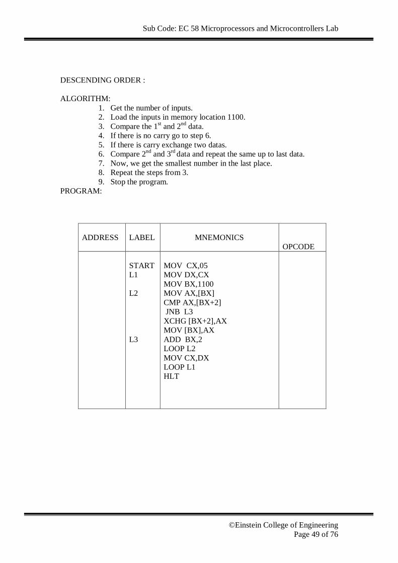
DESCENDING ORDER : ALGORITHM:
1. Get the number of inputs. 2. Load the inputs in memory location 1100. 3. Compare the 1st and 2nd data. 4. If there is no carry go to step 6. 5. If there is carry exchange two datas. 6. Compare 2nd and 3rd data and repeat the same up to last data. 7. Now, we get the smallest number in the last place. 8. Repeat the steps from 3. 9. Stop the program.
PROGRAM:
ADDRESS
LABEL
MNEMONICS
OPCODE
START L1 L2 L3
MOV CX,05 MOV DX,CX MOV BX,1100 MOV AX,[BX] CMP AX,[BX+2] JNB L3 XCHG [BX+2],AX MOV [BX],AX ADD BX,2 LOOP L2 MOV CX,DX LOOP L1 HLT

Sub Code: EC 58 Microprocessors and Microcontrollers Lab
©Einstein College of Engineering
Page 50 of 76
INPUT: OUTPUT: MANUAL CALCULATION: RESULT: Thus an ALP for sorting an array in ascending and descending order were executed using 8086 µp.

Sub Code: EC 58 Microprocessors and Microcontrollers Lab
©Einstein College of Engineering
Page 51 of 76
EX.NO. :10
DATE : STRING MANIPULATIONS
AIM: To write an ALP for performing string manipulation using 8086. APPARATUS REQUIRED:
8086 µp kit, keyboard, power chord. a) MOVING AN ARRAY OF DATA FROM SOURCE TO DESTINATION ALGORITHM:
1. Load the source and destination address. 2. Load the no of datas. 3. Facilitate auto increasing of the index register. 4. Move the string byte up to the last data. 5. Stop the program.
PROGRAM:
ADDRESS
LABEL
MNEMONICS
OPCODE
L1
MOV SI, 2000 MOV DI, 2100 MOV CX, 05 CLD MOV SB LOOP L1 HLT

Sub Code: EC 58 Microprocessors and Microcontrollers Lab
©Einstein College of Engineering
Page 52 of 76
b) STORING A DATA IN SET OF LOCATIONS: OBJECTIVE: To fill the locations in memory with the byte INPUT: OUTPUT: MANUAL CALCULATION:
ALGORITHM:
1. Load the number of inputs. 2. Load the destination address. 3. Load the data byte. 4. Facilitate auto incrementing of index register. 5. Store the data in the locations up to the last location. 6. Stop the program.

Sub Code: EC 58 Microprocessors and Microcontrollers Lab
©Einstein College of Engineering
Page 53 of 76
PROGRAM:
ADDRESS
LABEL
MNEMONICS
OPCODE
L1
MOV CX, 0006 MOV DI, 1100 MOV AX, 0034 CLD STO SB LOOP L1 HLT
c) CALCULATING THE LENGTH OF A STRING: OBJECTIVE: To find the number of character in a string ALGORITHM
1. Load the source address. 2. Clear the count register. 3. Load the assumed last data. 4. Increment the count. 5. Compare the data in source register with last data. 6. If both the datas are same, store the count in location 1100. 7. If both the datas are not same, increment the source address and load
the second data. 8. Repeat the steps from 4.
INPUT: OUTPUT:

Sub Code: EC 58 Microprocessors and Microcontrollers Lab
©Einstein College of Engineering
Page 54 of 76
MANUAL CALCULATION:
PROGRAM:
ADDRESS
LABEL
MNEMONICS
OPCODE
L1
MOV SI, 1200 MOV DX, FFFF MOV AH, FF INC DX MOV AL,[SI] INC SI CMP AH, AL JNZ L1 MOV [1100], DX HLT
Sub Code: EC 58 Microprocessors and Microcontrollers Lab
©Einstein College of Engineering
Page 55 of 76
RESULT: Thus the programs for string manipulation operations were performed by using 8086 µp.
Sub Code: EC 58 Microprocessors and Microcontrollers Lab
©Einstein College of Engineering
Page 56 of 76
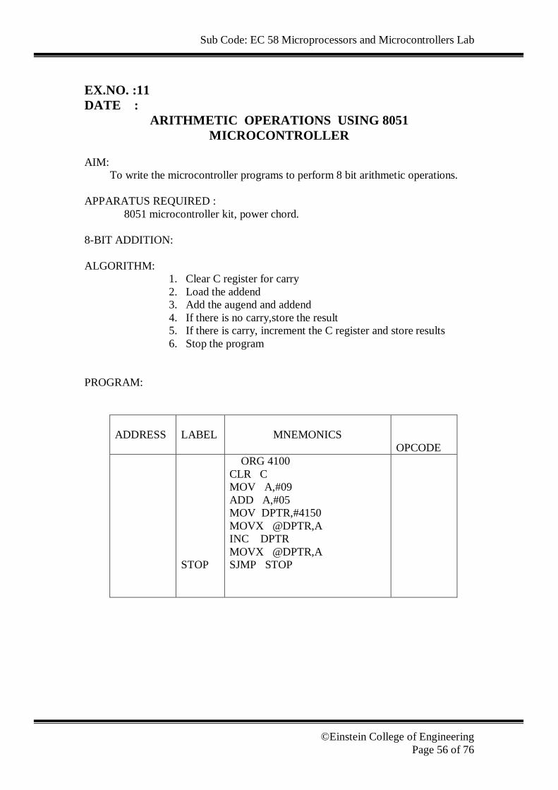
EX.NO. :11 DATE :
ARITHMETIC OPERATIONS USING 8051 MICROCONTROLLER
AIM: To write the microcontroller programs to perform 8 bit arithmetic operations. APPARATUS REQUIRED : 8051 microcontroller kit, power chord. 8-BIT ADDITION: ALGORITHM:
1. Clear C register for carry 2. Load the addend 3. Add the augend and addend 4. If there is no carry,store the result 5. If there is carry, increment the C register and store results 6. Stop the program
PROGRAM:
ADDRESS
LABEL
MNEMONICS
OPCODE
STOP
ORG 4100 CLR C MOV A,#09 ADD A,#05 MOV DPTR,#4150 MOVX @DPTR,A INC DPTR MOVX @DPTR,A SJMP STOP
Sub Code: EC 58 Microprocessors and Microcontrollers Lab
©Einstein College of Engineering
Page 57 of 76
INPUT: OUTPUT: MANUAL CALCULATION:

Sub Code: EC 58 Microprocessors and Microcontrollers Lab
©Einstein College of Engineering
Page 58 of 76
8-BIT SUBRACTION: ALGORITHM:
1. Clear C register for carry 2. Load the minuend 3. Subtact the subtrahend from minuend 4. If there is no carry,store the result 5. If there is carry, increment the C register and store results 6. Stop the program
PROGRAM:
ADDRESS
LABEL
MNEMONICS
OPCODE
STOP
ORG 4100 CLR C MOV A,#32 SUBB A,#30 MOV DPTR,#4150 MOVX @DPTR,A SJMP STOP
8-BIT MULTIPLICATION: ALGORITHM: 1. Load the two datas in A and B registers 2. Multiply the two datas 3. Store the result 4. Stop the program
Sub Code: EC 58 Microprocessors and Microcontrollers Lab
©Einstein College of Engineering
Page 59 of 76
INPUT: OUTPUT: MANUAL CALCULATION:
INPUT: OUTPUT: MANUAL CALCULATION:

Sub Code: EC 58 Microprocessors and Microcontrollers Lab
©Einstein College of Engineering
Page 60 of 76
PROGRAM:
ADDRESS
LABEL
MNEMONICS
OPCODE
STOP
ORG 4100 MOV A,#12 MOV B,#12 MUL AB MOV DPTR,#4500 MOVX @DPTR,A INC DPTR MOV A,B MOVX @DPTR,A SJMP STOP
8-BIT DIVISION: ALGORITHM:
1. Load the dividend and divisor 2. Divide the dividend by divisor 3. Store the quotient and reminder 4. Store the program
PROGRAM:
ADDRESS
LABEL
MNEMONICS
OPCODE
STOP
ORG 4100 MOV A,#12 MOV B,#12 DIV AB MOV DPTR,#4500 MOVX @DPTR,A INC DPTR MOV A,B MOVX @DPTR,A SJMP STOP
Sub Code: EC 58 Microprocessors and Microcontrollers Lab
©Einstein College of Engineering
Page 61 of 76
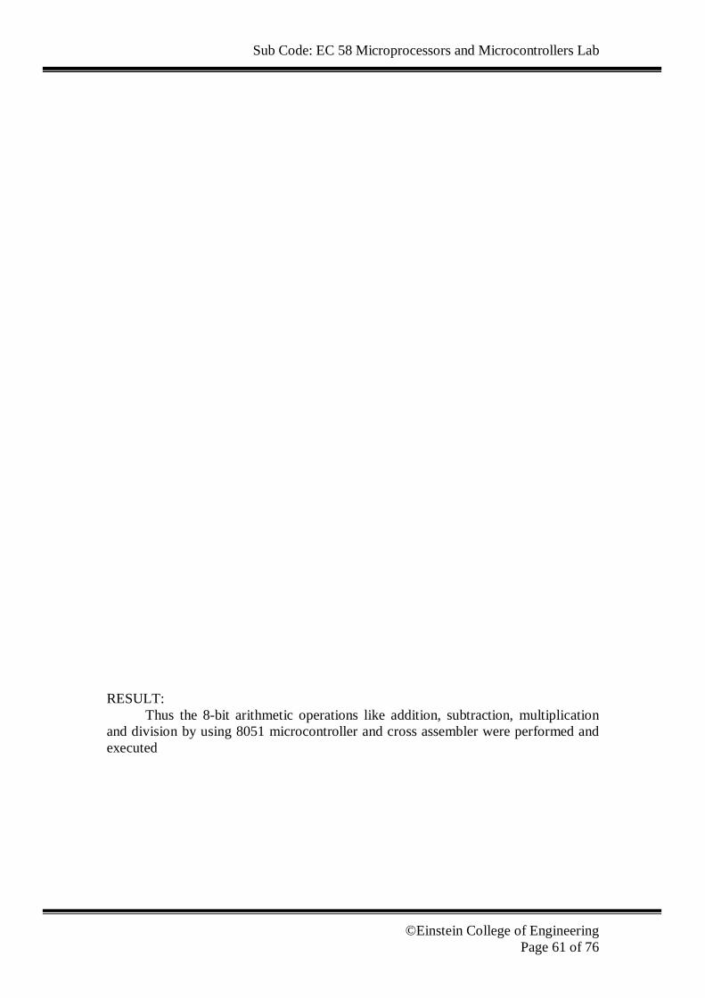
RESULT: Thus the 8-bit arithmetic operations like addition, subtraction, multiplication and division by using 8051 microcontroller and cross assembler were performed and executed

Sub Code: EC 58 Microprocessors and Microcontrollers Lab
©Einstein College of Engineering
Page 62 of 76
EX.NO. :12 DATE :
BIT MANIPULATIONS USING 8051 MICROCONTROLLER AIM: To write a program for setting and masking the bits in a b-bit data using 8051. APPARATUS REQUIRED: 8051 microcontroller kit, power chord
SETTING THE HIGHER ORDER BITS: ALGORITHM:
1. Load the given data 2. Set the bit by ORing that particular bit by 1 3. Store the result and stop the program.
PROGRAM:
ADDRESS
LABEL
MNEMONICS
OPCODE
STOP
ORG 4100 MOV A,#32 ORL A,#F0 MOV DPTR,#4500 MOVX@DPTR,A SJMP STOP
MASKING THE HIGHER ORDER BYTES: ALGORITHM:
1. Load the given data 2. Set the bit by ANDing that particular bit by 1 3. Store the result and stop the program.
PROGRAM:
ADDRESS
LABEL
MNEMONICS
OPCODE
STOP
ORG 4100 MOV A,#32 ANL A,#0F MOV DPTR,#4500 MOVX@DPTR,A SJMP STOP
Sub Code: EC 58 Microprocessors and Microcontrollers Lab
©Einstein College of Engineering
Page 63 of 76
RESULT: Thus the program for masking and setting the higher order bits by using 8051 microcontroller and cross assembler were performed and executed .

Sub Code: EC 58 Microprocessors and Microcontrollers Lab
©Einstein College of Engineering
Page 64 of 76
EX.NO. :13 DATE :
LOGICAL OPERATIONS USING 8051 MICROCONTROLLER AIM: To write a program for finding 1`s and 2`s complement of the given number and for the conversion of binary to gray using logical list. APPARATUS REQUIRED: 8051 microcontroller kit,power chord. 1`S AND 2`S COMPLEMENT: ALGORITHM:
1. Load the given data in accumulator 2. Complement the accumulator 3. Store the complement result 4. Increment the result by 1 and store 5. Stop the program
PROGRAM:
ADDRESS
LABEL
MNEMONICS
OPCODE
STOP
ORG 4100 MOV A,#12 CPL A MOV DPTR,#4200 MOVX@DPTR,A INC A INC DPTR MOVX@DPTR,A SJMP STOP
RESULT: Thus a program for performing logical operations using 8051 and cross assemler were executed

Sub Code: EC 58 Microprocessors and Microcontrollers Lab
©Einstein College of Engineering
Page 65 of 76

Sub Code: EC 58 Microprocessors and Microcontrollers Lab
©Einstein College of Engineering
Page 66 of 76

Sub Code: EC 58 Microprocessors and Microcontrollers Lab
©Einstein College of Engineering
Page 67 of 76

Sub Code: EC 58 Microprocessors and Microcontrollers Lab
©Einstein College of Engineering
Page 68 of 76

Sub Code: EC 58 Microprocessors and Microcontrollers Lab
©Einstein College of Engineering
Page 69 of 76
FAQ
1. Define opcode and operand?
2. What is Instruction cycle?
3. What is processor cycle (Machine cycle)?
4. Types of addressing modes?
5. What is immediate addressing mode?
6. What is direct addressing mode?
7. What is register addressing mode?
8. What is indirect addressing mode?
9. What is implied addressing mode?
Sub Code: EC 58 Microprocessors and Microcontrollers Lab
©Einstein College of Engineering
Page 70 of 76
10. What is the function of LXI H, 4000 instruction?
11. What is the function of INX H instruction?
12. What is the function of DCX H instruction?
13. What is the function of LHLD, 4200 instruction?
14. What is the function of XCHG instruction?
15. . What is the function of DAD instruction?
16. What is the function of SHLD instruction?
17. What is the function of SBB,B instruction?
18. What is the function of SPHL instruction?

Sub Code: EC 58 Microprocessors and Microcontrollers Lab
©Einstein College of Engineering
Page 71 of 76
19. What is the function of ORA D instruction?
20. What is the function of OUT & IN instruction?
21. What is the function of control& data register?
22. What is the difference between CALL &RET instruction?
23. Define interrupts?
24. What is the function of subroutine?
25. What is the function of RST instruction?
26. What is the function of JNC instruction?
27. What is the function of MVI instruction?
28. What is the function of STA instruction?

Sub Code: EC 58 Microprocessors and Microcontrollers Lab
©Einstein College of Engineering
Page 72 of 76
29. What is the function of MOV A, C instruction?
30. What is the function of INR instruction?
31. What is the function of DCR instruction?
32. What is the function of JNZ instruction?
33. Why interfacing is needed for I/0 devices?
34. List some of the features of INTEL 8259(Programmable Interrupt Controller)
35. What is the function of DEC DX instruction? 36. What is the function of LOOP instruction?
Sub Code: EC 58 Microprocessors and Microcontrollers Lab
©Einstein College of Engineering
Page 73 of 76
37. What is the function of JNB instruction? 38. What is the function of MOV instruction in 8086 processor? 39. What is the function of CLD instruction? 40. What is the function of STOSB instruction? 41. What is the function of INC DX, INC SI instruction? 42. What is the function of MOV DPTR, # 4150 instructions? 43. What is the function of MOVX @ DPTR, A instruction? 44. What is the function of SJMP instruction? 45. What is the function of ORL, ANL, and CPLA instruction?

Sub Code: EC 58 Microprocessors and Microcontrollers Lab
©Einstein College of Engineering
Page 74 of 76
46. What is the function of MUL AB instruction? 47. What is the function of INC DPTR instruction? 48. What is the function of LDA instruction? 49. What is the function of JMP instruction? 50. Give some examples of input devices to microprocessor-based system. 51. What is mean by microcontroller? 52. List the features of 8051 microcontroller? 53. What is the function of CMP M instruction? 54. What is the function of JNC instruction?

Sub Code: EC 58 Microprocessors and Microcontrollers Lab
©Einstein College of Engineering
Page 75 of 76
Sub Code: EC 58 Microprocessors and Microcontrollers Lab
©Einstein College of Engineering
Page 76 of 76