Embed Size (px)
Citation preview
8/14/2019 microprocessor and microcontroller module 3
http://slidepdf.com/reader/full/microprocessor-and-microcontroller-module-3 1/91
Microprocessors and Microcontrollers/Interfacing with 8086 Lecture Notes
Module 3
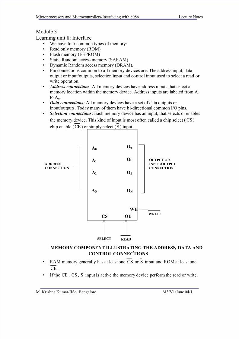
Learning unit 8: Interface• We have four common types of memory:
• Read only memory (ROM)
• Flash memory (EEPROM)
• Static Random access memory (SARAM)• Dynamic Random access memory (DRAM).
• Pin connections common to all memory devices are: The address input, data
output or input/outputs, selection input and control input used to select a read or write operation.
• Address connections: All memory devices have address inputs that select amemory location within the memory device. Address inputs are labeled from A0
to An.
• Data connections: All memory devices have a set of data outputs or input/outputs. Today many of them have bi-directional common I/O pins.
• Selection connections: Each memory device has an input, that selects or enables
the memory device. This kind of input is most often called a chip select ( CS ),
chip enable ( CE ) or simply select (S ) input.
O0A0
OA1
• RAM memory generally has at least one CS or S input and ROM at least one
CE .
• If the CE , CS , S input is active the memory device perform the read or write.
CS OE
A2
AN
O2
ON
OUTPUT OR
INPUT/OUTPUT
CONNECTION
ADDRESS
CONNECTION
WEWRITE
SELECT READ
MEMORY COMPONENT ILLUSTRATING THE ADDRESS DATA AND,
CONTROL CONNECTIONS
M. Krishna Kumar/IISc. Bangalore M3/V1/June 04/1
8/14/2019 microprocessor and microcontroller module 3
http://slidepdf.com/reader/full/microprocessor-and-microcontroller-module-3 2/91
Microprocessors and Microcontrollers/Interfacing with 8086 Lecture Notes
• If it is inactive the memory device cannot perform read or write operation.
• If more than one CS connection is present, all most be active to perform read or
write data.
• Control connections: A ROM usually has only one control input, while a RAMoften has one or two control inputs.
• The control input most often found on the ROM is the output enable (OE ) or gate
( G ), this allows data to flow out of the output data pins of the ROM.
• If OE and the selected input are both active, then the output is enable, if OE isinactive, the output is disabled at its high-impedance state.
• The OE connection enables and disables a set of three-state buffer located within
the memory device and must be active to read data.
• A RAM memory device has either one or two control inputs. If there is one
control input it is often called R/ W .
• This pin selects a read operation or a write operation only if the device is selected
by the selection input (CS ).
• If the RAM has two control inputs, they are usually labeled WE or W and OE
or G .
• ( WE ) write enable must be active to perform a memory write operation and OE
must be active to perform a memory read operation.
• When these two controls WE and OE are present, they must never be active at
the same time.• The ROM read only memory permanently stores programs and data and data was
always present, even when power is disconnected.
• It is also called as nonvolatile memory.• EPROM (erasable programmable read only memory) is also erasable if exposed
to high intensity ultraviolet light for about 20 minutes or less, depending upon thetype of EPROM.
• We have PROM (programmable read only memory)• RMM (read mostly memory) is also called the flash memory.
• The flash memory is also called as an EEPROM (electrically erasable
programmable ROM), EAROM (electrically alterable ROM), or a NOVROM(nonvolatile ROM).
• These memory devices are electrically erasable in the system, but require more
time to erase than a normal RAM.• EPROM contains the series of 27XXX contains the following part numbers :
2704(512 * 8), 2708(1K * 8), 2716(2K * 8), 2732(4K * 8), 2764(8K * 8),
27128(16K * 8) etc.• Each of these parts contains address pins, eight data connections, one or more
chip selection inputs (CE ) and an output enable pin ( OE ).
• This device contains 11 address inputs and 8 data outputs.
• If both the pin connection CE and OE are at logic 0, data will appear on the
output connection . If both the pins are not at logic 0, the data output connections
remains at their high impedance or off state.
• To read data from the EPROM Vpp pin must be placed at a logic 1.
M. Krishna Kumar/IISc. Bangalore M3/V1/June 04/2

8/14/2019 microprocessor and microcontroller module 3
http://slidepdf.com/reader/full/microprocessor-and-microcontroller-module-3 3/91
Microprocessors and Microcontrollers/Interfacing with 8086 Lecture Notes
24 Vcc1
2
3
4
5
6
7
8
9
12 13
23
22
2120
19
18
17
16
15
A7
A6 A
A5 A9
A Vpp
A3 CS
A
PIN CONFIGURATION OF 2716 EPROM
A1 PD/PGM
A10
A0 O7
O0 O6
O1 O5
OO2
O3GND
0 10A - A ADDRESSES
POWER DOWN / PROGRAMPD/PGM
CHIP SELECTCS
O0-O7 OUT PUTS
PIN NAMES
M. Krishna Kumar/IISc. Bangalore M3/V1/June 04/3

8/14/2019 microprocessor and microcontroller module 3
http://slidepdf.com/reader/full/microprocessor-and-microcontroller-module-3 4/91
Microprocessors and Microcontrollers/Interfacing with 8086 Lecture Notes
DATA OUTPUTSVcc O0 – O7
• Static RAM memory device retain data for as long as DC power is applied.
Because no special action is required to retain stored data, these devices are called
as static memory. They are also called volatile memory because they will notretain data without power.
• The main difference between a ROM and RAM is that a RAM is written under
normal operation, while ROM is programmed outside the computer and is onlynormally read.
• The SRAM stores temporary data and is used when the size of read/write memory
is relatively small.
VppGND
CHIP SELECTPOWER DOWN
AND PROGRAM
LOGIC
Y
DECODER
XDECODER
16,386 BIT
CELLMATRIX
Y-GATING
OUTPUT
BUFFERS
A0 - A10
ADDRESS
INPUTS
PD / PGM
CS
BLOCK DIAGRAM
M. Krishna Kumar/IISc. Bangalore M3/V1/June 04/4

8/14/2019 microprocessor and microcontroller module 3
http://slidepdf.com/reader/full/microprocessor-and-microcontroller-module-3 5/91
Microprocessors and Microcontrollers/Interfacing with 8086 Lecture Notes
A V247 1
2
3
4
5
6
7
8
9
10
11
12 13
14
23
22
21
20
19
18
17
16
15
PIN CONFIGURATION OF4016SRAM
A6 A8
A A9 5
A4 W
A3 G
A2 A10 A1 S
CC
A0 D8
D1 D7
D2 D6
D3 D5
VssD4
M. Krishna Kumar/IISc. Bangalore M3/V1/June 04/5

8/14/2019 microprocessor and microcontroller module 3
http://slidepdf.com/reader/full/microprocessor-and-microcontroller-module-3 6/91
Microprocessors and Microcontrollers/Interfacing with 8086 Lecture Notes
A
The control inputs of this RAM are slightly different from those presented earlier.
The OE pin is labeled G , the CS pin S and the WE pin W .
• This 4016 SRAM device has 11 address inputs and 8 data input/outputconnections.
Static RAM Interfacing
• The semiconductor RAM is broadly two types – Static RAM and Dynamic RAM.• The semiconductor memories are organised as two dimensional arrays of memory
locations.
• For example 4K * 8 or 4K byte memory contains 4096 locations, where eachlocations contains 8-bit data and only one of the 4096 locations can be selected at
a time. Once a location is selected all the bits in it are accessible using a group of
conductors called Data bus.
• For addressing the 4K bytes of memory, 12 address lines are required.• In general to address a memory location out of N memory locations, we will
require at least n bits of address, i.e. n address lines where n = Log 2 N.
• Thus if the microprocessor has n address lines, then it is able to address at the
most N locations of memory, where 2
n
=N. If out of N locations only P memorylocations are to be interfaced, then the least significant p address lines out of the
available n lines can be directly connected from the microprocessor to thememory chip while the remaining (n-p) higher order address lines may be used
for address decoding as inputs to the chip selection logic.
• The memory address depends upon the hardware circuit used for decoding the
chip select ( CS ). The output of the decoding circuit is connected with the CS pin
of the memory chip.
0 – A
ADDRESSES10 _
WRITE ENABLEW
S CHIP SELECT
DATA IN /DQ
0 _ DQ
8 DATA OUT
OUT PUT
G ENABLE
Vss GROUND
+ 5 VVccSUPPLY
PIN NAMES
M. Krishna Kumar/IISc. Bangalore M3/V1/June 04/6

8/14/2019 microprocessor and microcontroller module 3
http://slidepdf.com/reader/full/microprocessor-and-microcontroller-module-3 7/91
Microprocessors and Microcontrollers/Interfacing with 8086 Lecture Notes
• The general procedure of static memory interfacing with 8086 is briefly described
as follows:
1. Arrange the available memory chip so as to obtain 16- bit data bus width. Theupper 8-bit bank is called as odd address memory bank and the lower 8-bit bank is
called as even address memory bank.
2.
Connect available memory address lines of memory chip with those of themicroprocessor and also connect the memory RD and WR inputs to the
corresponding processor control signals. Connect the 16-bit data bus of the
memory bank with that of the microprocessor 8086.
3. The remaining address lines of the microprocessor, BHE and A0 are used for
decoding the required chip select signals for the odd and even memory banks. The
CS of memory is derived from the o/p of the decoding circuit.
• As a good and efficient interfacing practice, the address map of the system should
be continuous as far as possible, i.e. there should not be no windows in the map
and no fold back space should be allowed.• A memory location should have a single address corresponding to it, i.e. absolute
decoding should be preferred and minimum hardware should be used for decoding.
Dynamic RAM• Whenever a large capacity memory is required in a microcomputer system, the
memory subsystem is generally designed using dynamic RAM because there are
various advantages of dynamic RAM.• E.g. higher packing density, lower cost and less power consumption. A typical
static RAM cell may require six transistors while the dynamic RAM cell requires
only a transistors along with a capacitor. Hence it is possible to obtain higher packaging density and hence low cost units are available.
• The basic dynamic RAM cell uses a capacitor to store the charge as a
representation of data. This capacitor is manufactured as a diode that is reverse- biased so that the storage capacitance comes into the picture.
• This storage capacitance is utilized for storing the charge representation of data
but the reverse-biased diode has leakage current that tends to discharge the
capacitor giving rise to the possibility of data loss. To avoid this possible dataloss, the data stored in a dynamic RAM cell must be refreshed after a fixed time
interval regularly. The process of refreshing the data in RAM is called as Refresh
cycle.• The refresh activity is similar to reading the data from each and every cell of
memory, independent of the requirement of microprocessor. During this refresh
period all other operations related to the memory subsystem are suspended. Hence
the refresh activity causes loss of time, resulting in reduce system performance.• However keeping in view the advantages of dynamic RAM, like low power
consumption, high packaging density and low cost, most of the advanced
computing system are designed using dynamic RAM, at the cost of operatingspeed.
• A dedicated hardware chip called as dynamic RAM controller is the most
important part of the interfacing circuit.
M. Krishna Kumar/IISc. Bangalore M3/V1/June 04/7

8/14/2019 microprocessor and microcontroller module 3
http://slidepdf.com/reader/full/microprocessor-and-microcontroller-module-3 8/91
Microprocessors and Microcontrollers/Interfacing with 8086 Lecture Notes
• The Refresh cycle is different from the memory read cycle in the following
aspects.
1. The memory address is not provided by the CPU address bus, rather it isgenerated by a refresh mechanism counter called as refresh counter.
2. Unlike memory read cycle, more than one memory chip may be enabled at a time
so as to reduce the number of total memory refresh cycles.3. The data enable control of the selected memory chip is deactivated, and data is
not allowed to appear on the system data bus during refresh, as more than one
memory units are refreshed simultaneously. This is to avoid the data from thedifferent chips to appear on the bus simultaneously.
4. Memory read is either a processor initiated or an external bus master initiated and
carried out by the refresh mechanism.• Dynamic RAM is available in units of several kilobits to megabits of memory.
This memory is arranged internally in a two dimensional matrix array so that it
will have n rows and m columns. The row address n and column address m are
important for the refreshing operation.
•
For example, a typical 4K bit dynamic RAM chip has an internally arranged bitarray of dimension 64 * 64 , i.e. 64 rows and 64 columns. The row address and
column address will require 6 bits each. These 6 bits for each row address andcolumn address will be generated by the refresh counter, during the refresh cycles.
• A complete row of 64 cells is refreshed at a time to minimizes the refreshing time.
Thus the refresh counter needs to generate only row addresses. The row addressare multiplexed, over lower order address lines.
• The refresh signals act to control the multiplexer, i.e. when refresh cycle is in
process the refresh counter puts the row address over the address bus for
refreshing. Otherwise, the address bus of the processor is connected to the address bus of DRAM, during normal processor initiated activities.
• A timer, called refresh timer, derives a pulse for refreshing action after each
refresh interval.
• Refresh interval can be qualitatively defined as the time for which a dynamic
RAM cell can hold data charge level practically constant, i.e. no data loss takes place.
• Suppose the typical dynamic RAM chip has 64 rows, then each row should be
refreshed after each refresh interval or in other words, all the 64 rows are torefreshed in a single refresh interval.
• This refresh interval depends upon the manufacturing technology of the dynamic
RAM cell. It may range anywhere from 1ms to 3ms.• Let us consider 2ms as a typical refresh time interval. Hence, the frequency of the
refresh pulses will be calculated as follows:
• Refresh Time (per row) tr = (2 * 10 -3) / 64.
• Refresh Frequency fr = 64 / (2 * 10 -3) = 32 * 103 Hz.• The following block diagram explains the refreshing logic and 8086 interfacing
with dynamic RAM.
• Each chip is of 16K * 1-bit dynamic RAM cell array. The system contains two16K byte dynamic RAM units. All the address and data lines are assumed to be
available from an 8086 microprocessor system.
M. Krishna Kumar/IISc. Bangalore M3/V1/June 04/8

8/14/2019 microprocessor and microcontroller module 3
http://slidepdf.com/reader/full/microprocessor-and-microcontroller-module-3 9/91
Microprocessors and Microcontrollers/Interfacing with 8086 Lecture Notes
• The OE pin controls output data buffer of the memory chips. The CE pins are
active high chip selects of memory chips. The refresh cycle starts, if the refresh
output of the refresh timer goes high, OE and CE also tend to go high.
• The high CE enables the memory chip for refreshing, while high OE prevents thedata from appearing on the data bus, as discussed in memory refresh cycle. The
16K * 1-bit dynamic RAM has an internal array of 128*128 cells, requiring 7 bitsfor row address. The lower order seven lines A0-A6 are multiplexed with therefresh counter output A10-A16.
16K*1
A7 – A13
16K*1 16K*1 16K*1 16K*1 16K*1 16K*1 16K*1
OE CE
Ref. Add
Counter Refresh
Refresh
timer
To transreceivers
A15 A14
CE1 CE2
Address Deciding
logic
7 bit
bus
MUX
A7 – A13
CE1
CE2
A0-A6
OE CE OE CE OE CE OE CE OE CE OE CE OE CE
A6 – A0
16K*1
A7 – A13
16K*1 16K*1 16K*1 16K*1 16K*1 16K*116K*1
A6 – A0
OE CE OE CE CE OE CE OE CE OE OE CECEOE CEOE
Ar0
–
Ar6
Dynamic RAM Refreshing Logic
M. Krishna Kumar/IISc. Bangalore M3/V1/June 04/9

8/14/2019 microprocessor and microcontroller module 3
http://slidepdf.com/reader/full/microprocessor-and-microcontroller-module-3 10/91
8/14/2019 microprocessor and microcontroller module 3
http://slidepdf.com/reader/full/microprocessor-and-microcontroller-module-3 11/91
Microprocessors and Microcontrollers/Interfacing with 8086 Lecture Notes
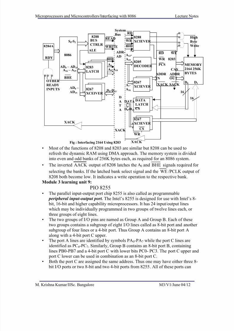
• Intel’s 8203 is a dynamic RAM controller that support 16K or 64K dynamic
RAM chip. This selection is done using pin 16K/64K. If it is high, the 8203 is
configured to control 16K dynamic RAM, else it controls 64K dynamic RAM.The address inputs of 8203 controller accepts address lines A1 to A16 on lines
AL0-AL7 and AH0-AH7.
• The A0 lines is used to select the even or odd bank. The RD and WR signalsdecode whether the cycle is a memory read or memory write cycle and areaccepted as inputs to 8203 from the microprocessor.
• The WE signal specifies the memory write cycle and is not output from 8203 that
drives the WE input of dynamic RAM memory chip. The 0OUT – 7OUT set of
eight pins is an 8-bit output bus that carries multiplexed row and column
addresses are derived from the address lines A1-A16 accepted by the controller onits inputs AL0-AL7 and AH0-AH7.
• An external crystal may be applied between X0 and X1 pins, otherwise with the
OP2 pin at +12V, a clock signal may be applied at pin CLK.
• The PCS pin accepts the chip select signal derived by an address decoder. The
REFREQ pin is used whenever the memory refresh cycle is to be initiated by an
external signal.
• The XACK signal indicates that data is available during a read cycle or it has
been written if it is a write cycle. It can be used as a strobe for data latches or as a
ready signal to the processor.
• The SACK output signal marks the beginning of a memory access cycle.
• If a memory request is made during a memory refresh cycle, the SACK signal is
delayed till the starring of memory read or write cycle.
• Following fig shows the 8203 can be used to control a 256K bytes memorysubsystem for a maximum mode 8086 microprocessor system.
• This design assumes that data and address busses are inverted and latched, hencethe inverting buffers and inverting latches are used (8283-inverting buffer and
8287- inverting latch).
M. Krishna Kumar/IISc. Bangalore M3/V1/June 04/11
8/14/2019 microprocessor and microcontroller module 3
http://slidepdf.com/reader/full/microprocessor-and-microcontroller-module-3 12/91
Microprocessors and Microcontrollers/Interfacing with 8086 Lecture Notes
• Most of the functions of 8208 and 8203 are similar but 8208 can be used to
refresh the dynamic RAM using DMA approach. The memory system is divided
into even and odd banks of 256K bytes each, as required for an 8086 system.
• The inverted AACK output of 8208 latches the A0 and BHE signals required for
selecting the banks. If the latched bank select signal and the WE /PCLK output of
8208 both become low. It indicates a write operation to the respective bank.
Module 3 learning unit 9:
PIO 8255
• The parallel input-output port chip 8255 is also called as programmable peripheral input-output port. The Intel’s 8255 is designed for use with Intel’s 8- bit, 16-bit and higher capability microprocessors. It has 24 input/output lines
which may be individually programmed in two groups of twelve lines each, or
three groups of eight lines.• The two groups of I/O pins are named as Group A and Group B. Each of these
two groups contains a subgroup of eight I/O lines called as 8-bit port and another
subgroup of four lines or a 4-bit port. Thus Group A contains an 8-bit port Aalong with a 4-bit port C upper.
• The port A lines are identified by symbols PA0-PA7 while the port C lines are
identified as PC4-PC7. Similarly, Group B contains an 8-bit port B, containing
lines PB0-PB7 and a 4-bit port C with lower bits PC0- PC3. The port C upper and port C lower can be used in combination as an 8-bit port C.
• Both the port C are assigned the same address. Thus one may have either three 8-
bit I/O ports or two 8-bit and two 4-bit ports from 8255. All of these ports can
XACK
XACK
XACK
OTHER
READY
INPUTS
8284A
RDY
AD0 –
AD15
AD – AD150
A16 – A19
BHE
8086
S0-S2
8288BUS
CTRLR
ALE
8267
XCEIVER
8283
LATCH
D0-D15
A0-A19
A0
BHE
WRITE
READ
System
Bus RD
8288
XCIEVER
8205
DECODER
8267
XCIEVER
DATA
LATCH
CS
8267
XCIEVER
CS
WR
DATA
D0-D15
MEMORY
2164 256K
BYTES
D0 D1
16
16
A1-
A16
A12-
A19
A0
WR
BHE
D
A
T
A
ADR-
AD
RD
WR
PCS
ADDR
IN
XACK SACK
8203
WE
ADDR
OUT
CAS
Fig : Interfacing 2164 Using 8203
High
Byte
Write
M. Krishna Kumar/IISc. Bangalore M3/V1/June 04/12

8/14/2019 microprocessor and microcontroller module 3
http://slidepdf.com/reader/full/microprocessor-and-microcontroller-module-3 13/91
Microprocessors and Microcontrollers/Interfacing with 8086 Lecture Notes
function independently either as input or as output ports. This can be achieved by
programming the bits of an internal register of 8255 called as control word
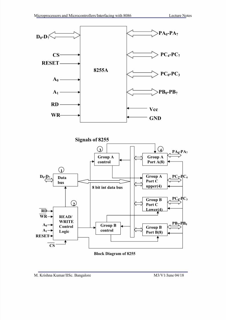
register (CWR).• The internal block diagram and the pin configuration of 8255 are shown in fig.
• The 8-bit data bus buffer is controlled by the read/write control logic. The
read/write control logic manages all of the internal and external transfers of bothdata and control words.
• RD , WR , A1, A0 and RESET are the inputs provided by the microprocessor to
the READ/ WRITE control logic of 8255. The 8-bit, 3-state bidirectional buffer is
used to interface the 8255 internal data bus with the external system data bus.
• This buffer receives or transmits data upon the execution of input or outputinstructions by the microprocessor. The control words or status information is also
transferred through the buffer.
• The signal description of 8255 are briefly presented as follows :• PA7-PA0: These are eight port A lines that acts as either latched output or
buffered input lines depending upon the control word loaded into the control word
register.• PC7-PC4 : Upper nibble of port C lines. They may act as either output latches or
input buffers lines.
• This port also can be used for generation of handshake lines in mode 1 or mode 2.• PC3-PC0 : These are the lower port C lines, other details are the same as PC7-PC4
lines.
• PB0-PB7 : These are the eight port B lines which are used as latched output lines
or buffered input lines in the same way as port A.
• RD : This is the input line driven by the microprocessor and should be low toindicate read operation to 8255.
• WR : This is an input line driven by the microprocessor. A low on this line
indicates write operation.
• CS : This is a chip select line. If this line goes low, it enables the 8255 to respond
to RD and WR signals, otherwise RD and WR signal are neglected.
• A1-A0 : These are the address input lines and are driven by the microprocessor.
These lines A1-A0 with RD , WR and CS from the following operations for
8255. These address lines are used for addressing any one of the four registers, i.e.three ports and a control word register as given in table below.
• In case of 8086 systems, if the 8255 is to be interfaced with lower order data bus,
the A0 and A1 pins of 8255 are connected with A1 and A2 respectively.
• D0-D7 : These are the data bus lines those carry data or control word to/from the
microprocessor.• RESET : A logic high on this line clears the control word register of 8255. All
ports are set as input ports by default after reset.
M. Krishna Kumar/IISc. Bangalore M3/V1/June 04/13

8/14/2019 microprocessor and microcontroller module 3
http://slidepdf.com/reader/full/microprocessor-and-microcontroller-module-3 14/91
Microprocessors and Microcontrollers/Interfacing with 8086 Lecture Notes
A1 A0 Input (Read) cycle
Block Diagram of 8255 (Architecture)
• It has a 40 pins of 4 groups.1. Data bus buffer
2. Read Write control logic
3. Group A and Group B controls
4. Port A, B and C• Data bus buffer: This is a tristate bidirectional buffer used to interface the 8255 to
system databus. Data is transmitted or received by the buffer on execution of
input or output instruction by the CPU.• Control word and status information are also transferred through this unit.
• Read/Write control logic: This unit accepts control signals (RD , WR ) and also
inputs from address bus and issues commands to individual group of control
blocks (Group A, Group B).• It has the following pins.
a) CS – Chipselect : A low on this PIN enables the communication between CPU
and 8255.
b) RD (Read) – A low on this pin enables the CPU to read the data in the ports or
the status word through data bus buffer.
RD WR CS0 1 0 Port A to Data bus00
Port B to Data bus0 1 0
Port C to Data bus
CWR to Data bus
1
1
0
0 0
0
1 0
11 0 1
A1 A0 Output (Write) cycleRD WR CS0 0 0 Data bus to Port A1 0
Data bus to Port B10 0
Data bus to Port C
Data bus to CWR
00
0 11
1
01
01
01
A1 A0 FunctionRD WR CSX X 1 X Data bus tristatedX
Data bus tristated1 1 0 XX
Control Word Register
M. Krishna Kumar/IISc. Bangalore M3/V1/June 04/14

8/14/2019 microprocessor and microcontroller module 3
http://slidepdf.com/reader/full/microprocessor-and-microcontroller-module-3 15/91
Microprocessors and Microcontrollers/Interfacing with 8086 Lecture Notes
c) WR (Write) : A low on this pin, the CPU can write data on to the ports or on to
the control register through the data bus buffer.
d) RESET: A high on this pin clears the control register and all ports are set to the
input mode
e) A0 and A1 (Address pins): These pins in conjunction with RD and WR pins
control the selection of one of the 3 ports.• Group A and Group B controls : These block receive control from the CPU and
issues commands to their respective ports.
• Group A - PA and PCU (PC7 –PC4)
• Group B - PCL (PC3 – PC0)• Control word register can only be written into no read operation of the CW
register is allowed.• a) Port A: This has an 8 bit latched/buffered O/P and 8 bit input latch. It can be
programmed in 3 modes – mode 0, mode 1, mode 2.
b) Port B: This has an 8 bit latched / buffered O/P and 8 bit input latch. It can be programmed in mode 0, mode1.
c) Port C : This has an 8 bit latched input buffer and 8 bit out put latched/buffer.This port can be divided into two 4 bit ports and can be used as control signals for port A
and port B. it can be programmed in mode 0.
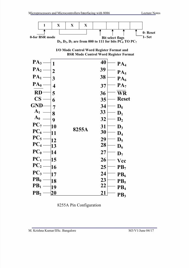
Modes of Operation of 8255• These are two basic modes of operation of 8255. I/O mode and Bit Set-Reset
mode (BSR).
• In I/O mode, the 8255 ports work as programmable I/O ports, while in BSR modeonly port C (PC0-PC7) can be used to set or reset its individual port bits.
• Under the I/O mode of operation, further there are three modes of operation of
8255, so as to support different types of applications, mode 0, mode 1 and mode2.
• BSR Mode: In this mode any of the 8-bits of port C can be set or reset dependingon D0 of the control word. The bit to be set or reset is selected by bit select flags
D3, D2 and D1 of the CWR as given in table.
• I/O Modes :a) Mode 0 (Basic I/O mode): This mode is also called as basic input/output mode.
This mode provides simple input and output capabilities using each of the three ports.
Data can be simply read from and written to the input and output ports respectively, after appropriate initialisation.
M. Krishna Kumar/IISc. Bangalore M3/V1/June 04/15

8/14/2019 microprocessor and microcontroller module 3
http://slidepdf.com/reader/full/microprocessor-and-microcontroller-module-3 16/91
8/14/2019 microprocessor and microcontroller module 3
http://slidepdf.com/reader/full/microprocessor-and-microcontroller-module-3 17/91
Microprocessors and Microcontrollers/Interfacing with 8086 Lecture Notes
1 X X X
0- Reset
1- Set0-for BSR mode Bit select flagsD3, D2, D1 are from 000 to 111 for bits PC0 TO PC7
I/O Mode Control Word Register Format and
BSR Mode Control Word Register Format
2019
18
17
16
15
14
1312
11
10
9
8
7
65
4
3
2
1
2122
23
24
25
26
27
2829
3031
33
32
34
3635
37
38
39
40
PB3
PB4
PB5
PB6
PB7
Vcc
D7
D6D5
D4
D3
D2
D1
D0
ResetWR
PA7
PA6
PA5
PA4
PB2PB1
PB0
PC3
PC2
PC1
PC0
PC4
PC5
PC6
PC7
A0
A1
GND
CSRD
PA0
PA1
PA2
PA3
8255A
8255A Pin Configuration
M. Krishna Kumar/IISc. Bangalore M3/V1/June 04/17
8/14/2019 microprocessor and microcontroller module 3
http://slidepdf.com/reader/full/microprocessor-and-microcontroller-module-3 18/91
Microprocessors and Microcontrollers/Interfacing with 8086 Lecture Notes
PA0-PA7D0-D7
PC4-PC7CSRESET
8255APC0-PC3
A0
A1 PB0-PB7
RD
VccWR GND
Signals of 8255
3 4 PA0-PA7
Group A
control
Group A
Port A(8)
1
Group A
Port C
upper(4)
D0-D7 PC7-PC4Data
bus
8 bit int data bus
PC0-PC3Group B
Port C
Lower(4)
2
RD
WR READ/
WRITE
Control
Logic
PB7-PB0A0 Group Bcontrol
Group B
Port B(8)A1
RESET
CS
Block Diagram of 8255
M. Krishna Kumar/IISc. Bangalore M3/V1/June 04/18

8/14/2019 microprocessor and microcontroller module 3
http://slidepdf.com/reader/full/microprocessor-and-microcontroller-module-3 19/91
Microprocessors and Microcontrollers/Interfacing with 8086 Lecture Notes
D7 D6 D5 D4 D3 D2 D1 D0
Mode for
Port AMode
for PBPA PC U PB PC L
Mode Set flag
1- active 0-
BSR mode
Group - A Group - B
1 InputPC u 1 InputPCL
b) Mode 1: (Strobed input/output mode) In this mode the handshaking control the input
and output action of the specified port. Port C lines PC0-PC2, provide strobe or
handshake lines for port B. This group which includes port B and PC0-PC2 is called asgroup B for Strobed data input/output. Port C lines PC3-PC5 provide strobe lines for port
A.
This group including port A and PC3-PC5 from group A. Thus port C is utilized for
generating handshake signals. The salient features of mode 1 are listed as follows:
1. Two groups – group A and group B are available for strobed data transfer.2. Each group contains one 8-bit data I/O port and one 4-bit control/data port.
3. The 8-bit data port can be either used as input and output port. The inputs andoutputs both are latched.
4. Out of 8-bit port C, PC0-PC2 are used to generate control signals for port B and
PC3-PC5 are used to generate control signals for port A. the lines PC6, PC7 may be used as independent data lines.
• The control signals for both the groups in input and output modes are
explained as follows:
Input control signal definitions (mode 1):
• STB (Strobe input) – If this lines falls to logic low level, the data available at 8-bit
input port is loaded into input latches.
• IBF (Input buffer full) – If this signal rises to logic 1, it indicates that data has
been loaded into latches, i.e. it works as an acknowledgement. IBF is set by a low
on STB and is reset by the rising edge of RD input.
• INTR (Interrupt request) – This active high output signal can be used to interruptthe CPU whenever an input device requests the service. INTR is set by a high
Control Word Format of 8255
PB
Mode
Select
0 Output1 Input
0 Output
1 InputPA0 Output00 – mode 0
0 Output
Mode
Select
of PA
01 – mode 1 0 mode- 0
10 – mode 2 1 mode- 1
M. Krishna Kumar/IISc. Bangalore M3/V1/June 04/19

8/14/2019 microprocessor and microcontroller module 3
http://slidepdf.com/reader/full/microprocessor-and-microcontroller-module-3 20/91
Microprocessors and Microcontrollers/Interfacing with 8086 Lecture Notes
STB pin and a high at IBF pin. INTE is an internal flag that can be controlled by
the bit set/reset mode of either PC4(INTEA) or PC2(INTEB) as shown in fig.
• INTR is reset by a falling edge of RD input. Thus an external input device can berequest the service of the processor by putting the data on the bus and sending the
strobe signal.
Output control signal definitions (mode 1) : • OBF (Output buffer full) – This status signal, whenever falls to low, indicates that
CPU has written data to the specified output port. The OBF flip-flop will be set by
a rising edge of WR signal and reset by a low going edge at the ACK input.
• ACK (Acknowledge input) – ACK signal acts as an acknowledgement to be
given by an output device. ACK signal, whenever low, informs the CPU that the
data transferred by the CPU to the output device through the port is received bythe output device.
• INTR (Interrupt request) – Thus an output signal that can be used to interrupt the
CPU when an output device acknowledges the data received from the CPU. INTR is set when ACK, OBF and INTE are 1. It is reset by a falling edge on WR input.
The INTEA and INTEB flags are controlled by the bit set-reset mode of PC6 andPC2 respectively.
D0D1D2D3D4D5D6D7
1 1 1/000 X X X
Input control signal definitions in Mode
1
1 X X X 1X 1 X
D5 D4 D1 D0D7 D6 D3 D2
1 - Input0 - Output
For PC6 – PC7
PB0 – PB7PA0 – PA7
Mode 1 Control Word Group A
I/P
Mode 1 Control Word Group B
I/P
INTEA INTEBPC4 PC2 STBBSTBA
PC5 PC1IBFA IBFB
PC0 INTR PC3 INTR A
PC6 – PC7 I/ORD
RD
M. Krishna Kumar/IISc. Bangalore M3/V1/June 04/20

8/14/2019 microprocessor and microcontroller module 3
http://slidepdf.com/reader/full/microprocessor-and-microcontroller-module-3 21/91
Microprocessors and Microcontrollers/Interfacing with 8086 Lecture Notes
STB
IBF
INTR
RD
DATA
from
Mode 1 Strobed Input Data Transfer
WR
OBF
INTR
ACK
Data OP to
Port
Mode 1 Strobed Data Output
M. Krishna Kumar/IISc. Bangalore M3/V1/June 04/21

8/14/2019 microprocessor and microcontroller module 3
http://slidepdf.com/reader/full/microprocessor-and-microcontroller-module-3 22/91
Microprocessors and Microcontrollers/Interfacing with 8086 Lecture Notes
Output control signal definitions Mode 1
• Mode 2 (Strobed bidirectional I/O): This mode of operation of 8255 is alsocalled as strobed bidirectional I/O. This mode of operation provides 8255 with an
additional features for communicating with a peripheral device on an 8-bit data
bus. Handshaking signals are provided to maintain proper data flow and
synchronization between the data transmitter and receiver. The interrupt
generation and other functions are similar to mode 1.• In this mode, 8255 is a bidirectional 8-bit port with handshake signals. The Rd
and WR signals decide whether the 8255 is going to operate as an input port or output port.
• The Salient features of Mode 2 of 8255 are listed as follows:
1. The single 8-bit port in group A is available.2. The 8-bit port is bidirectional and additionally a 5-bit control port is available.
3. Three I/O lines are available at port C.(PC2 – PC0)
4. Inputs and outputs are both latched.5. The 5-bit control port C (PC3-PC7) is used for generating / accepting handshake
signals for the 8-bit data transfer on port A.
• Control signal definitions in mode 2:
• INTR – (Interrupt request) As in mode 1, this control signal is active high and isused to interrupt the microprocessor to ask for transfer of the next data byte
to/from it. This signal is used for input (read) as well as output (write) operations.
• Control Signals for Output operations:
• OBF (Output buffer full) – This signal, when falls to low level, indicates that the
CPU has written data to port A.
D0D1D2D3D4D5D6D7
1 1 1/000 X X X 1 X X X X 1 0 X
D5 D4 D1 D0D7 D6 D3 D2
1 - Input0 - Output
For PC4 – PC5
PB0 –
PB7
PA0 – PA7
Mode 1 Control Word Group A Mode 1 Control Word Group B
INTEA INTEB PC1
PC2
PC0 INTR B
ACK B
OBF
I/O
INTR A
ACK A
OBFPC6
PC7
PC3
PC4 – PC5WR
M. Krishna Kumar/IISc. Bangalore M3/V1/June 04/22
8/14/2019 microprocessor and microcontroller module 3
http://slidepdf.com/reader/full/microprocessor-and-microcontroller-module-3 23/91
Microprocessors and Microcontrollers/Interfacing with 8086 Lecture Notes
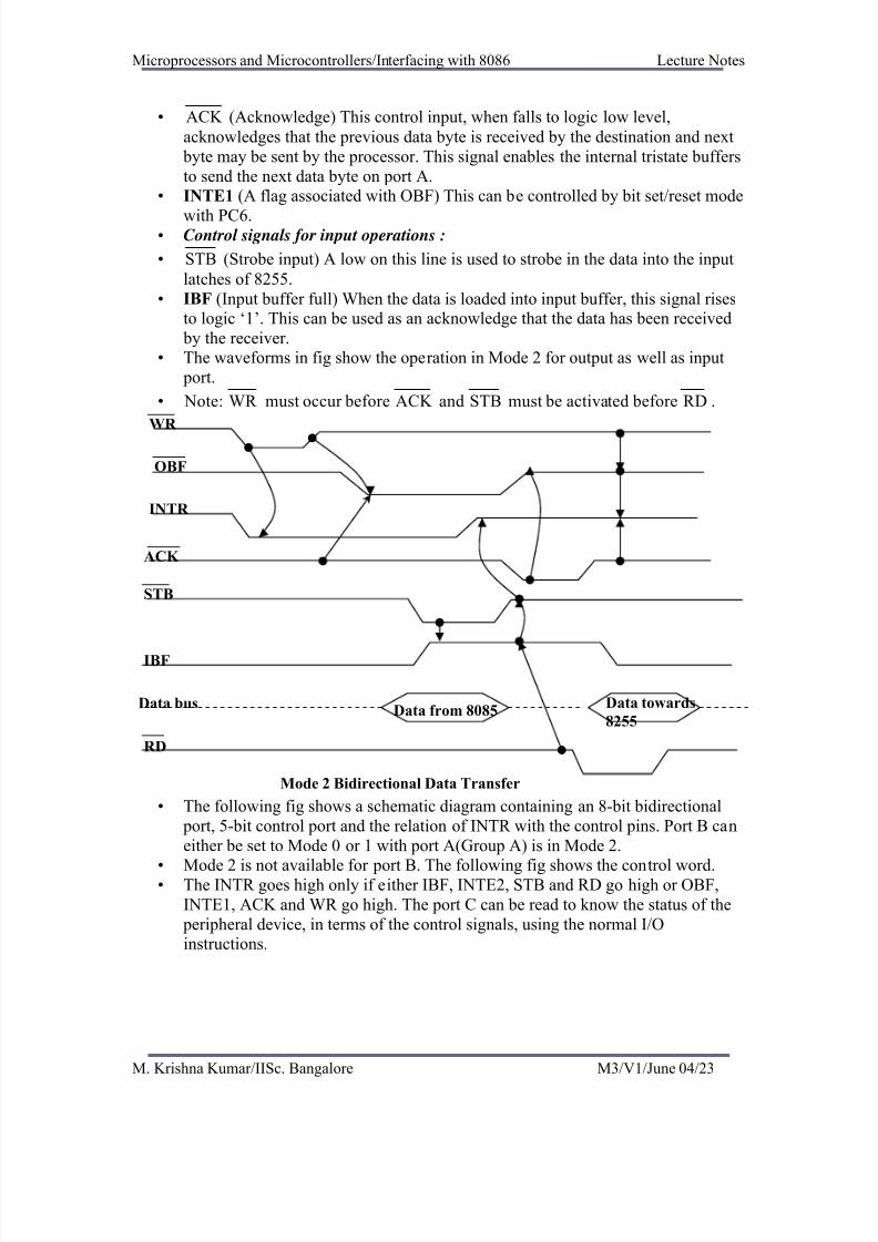
• ACK (Acknowledge) This control input, when falls to logic low level,
acknowledges that the previous data byte is received by the destination and next
byte may be sent by the processor. This signal enables the internal tristate buffers
to send the next data byte on port A.• INTE1 (A flag associated with OBF) This can be controlled by bit set/reset mode
with PC6.• Control signals for input operations :
• STB (Strobe input) A low on this line is used to strobe in the data into the input
latches of 8255.
• IBF (Input buffer full) When the data is loaded into input buffer, this signal risesto logic ‘1’. This can be used as an acknowledge that the data has been received
by the receiver.• The waveforms in fig show the operation in Mode 2 for output as well as input
port.
• Note: WR must occur before ACK and STB must be activated before RD .
• The following fig shows a schematic diagram containing an 8-bit bidirectional
port, 5-bit control port and the relation of INTR with the control pins. Port B can
either be set to Mode 0 or 1 with port A(Group A) is in Mode 2.
• Mode 2 is not available for port B. The following fig shows the control word.• The INTR goes high only if either IBF, INTE2, STB and RD go high or OBF,
INTE1, ACK and WR go high. The port C can be read to know the status of the
peripheral device, in terms of the control signals, using the normal I/Oinstructions.
WR
OBF
INTR
ACK
STB
IBF
Data towards
8255
Data busData from 8085
RD
Mode 2 Bidirectional Data Transfer
M. Krishna Kumar/IISc. Bangalore M3/V1/June 04/23
8/14/2019 microprocessor and microcontroller module 3
http://slidepdf.com/reader/full/microprocessor-and-microcontroller-module-3 24/91
Microprocessors and Microcontrollers/Interfacing with 8086 Lecture Notes
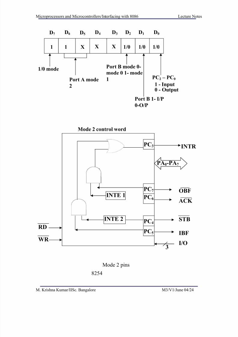
D6 D4 D3 D2 D1 D0D7 D5
8254
1 X X X1 1/0 1/0 1/0
1 - Input0 - Output
PC2 – PC0
1/0 mode
Port A mode
2
Port B mode 0-
mode 0 1- mode
1
Port B 1- I/P
0-O/P
Mode 2 control word
PC3
WR
RD
PC7
PC6
PC4
PC5
INTE 1
I/OIBF
STB
ACK
OBF
INTR
PA0-PA7
INTE 2
3
Mode 2 pins
M. Krishna Kumar/IISc. Bangalore M3/V1/June 04/24

8/14/2019 microprocessor and microcontroller module 3
http://slidepdf.com/reader/full/microprocessor-and-microcontroller-module-3 25/91
Microprocessors and Microcontrollers/Interfacing with 8086 Lecture Notes
• Compatible with All Intel and Most other Microprocessors
• Handles Inputs from DC to 10 MHz
• 8 MHz 8254• 10 MHz 8254-2
• Status Read-Back Command
•
Six Programmable Counter Modes• Three Independent 16-Bit Counters
• Binary or BCD Counting
• Single a 5V Supply• Standard Temperature Range
• The Intel 8254 is a counter/timer device designed to solve the common timing
control problems in microcomputer system design.• It provides three independent 16-bit counters, each capable of handling clock
inputs up to 10 MHz.
• All modes are software programmable. The 8254 is a superset of the 8253.The
8254 uses HMOS technology and comes in a 24-pin plastic or CERDIP package.
M. Krishna Kumar/IISc. Bangalore M3/V1/June 04/25

8/14/2019 microprocessor and microcontroller module 3
http://slidepdf.com/reader/full/microprocessor-and-microcontroller-module-3 26/91
Microprocessors and Microcontrollers/Interfacing with 8086 Lecture Notes
Figure 1. Pin Configuration
M. Krishna Kumar/IISc. Bangalore M3/V1/June 04/26

8/14/2019 microprocessor and microcontroller module 3
http://slidepdf.com/reader/full/microprocessor-and-microcontroller-module-3 27/91
Microprocessors and Microcontrollers/Interfacing with 8086 Lecture Notes
Figure 2. 8254 Block
Pin Description
Pin
No.
Type Name and FunctionSymbol
D7-D0 DATA: Bi-directional three state data bus
lines, connected to system data bus.
1 - 8 I/O
ICLK 0 9 CLOCK 0: Clock input of Counter 0.
OUT 0 10 O OUTPUT 0: Output of Counter 0.
GATE 0 11 I GATE 0: Gate input of Counter 0.
12GND GROUND: Power supply connection.
VCC 24 POWER: A 5V power supply connection.WR WRITE CONTROL: This input is low during
CPU write operations.23 I
RD 22 IREAD CONTROL: This input is low during
CPU read operations.
M. Krishna Kumar/IISc. Bangalore M3/V1/June 04/27

8/14/2019 microprocessor and microcontroller module 3
http://slidepdf.com/reader/full/microprocessor-and-microcontroller-module-3 28/91
Microprocessors and Microcontrollers/Interfacing with 8086 Lecture Notes
Functional Description• The 8254 is a programmable interval timer/counter designed for use with Intel
microcomputer systems.
• It is a general purpose, multi-timing element that can be treated as an array of I/O
ports in the system software.• The 8254 solves one of the most common problems in any microcomputer
system, the generation of accurate time delays under software control. Instead of setting up timing loops in software, the programmer configures the 8254 to match
his requirements and programs one of the counters for the desired delay.
• After the desired delay, the 8254 will interrupt the CPU. Software overhead is
minimal and variable length delays can easily be accommodated.• Some of the other counter/timer functions common to microcomputers which can
be implemented with the 8254 are:
• Real time clock • Event-counter
• Digital one-shot
• Programmable rate generator • Square wave generator
CS 21 ICHIP SELECT: A low on this input enables the
8254 to respond to RD and WR signals. RD and
WR are ignored otherwise.
ADDRESS: Used to select one of the three
Counters or the Control Word Register for read
or write operations. Normally connected to the
system address bus.
A1, A0 20 – 9 I
A1 A0 Selects
0 0 Counter 0
0 1 Counter 1
1 0 Counter 2
1 1 Control Word Register
18 I CLOCK 2: Clock input of Counter 2.CLK 2
OUT 2 17 O OUT 2: Output of Counter 2.
GATE 2 16 I GATE 2: Gate input of Counter 2.
CLK 1 15 CLOCK 1: Clock input of Counter 1.I
14 IGATE 1 GATE 1: Gate input of Counter 1.
OUT 1 OUT 1 O OUT 1: Output of Counter 1.
M. Krishna Kumar/IISc. Bangalore M3/V1/June 04/28

8/14/2019 microprocessor and microcontroller module 3
http://slidepdf.com/reader/full/microprocessor-and-microcontroller-module-3 29/91
Microprocessors and Microcontrollers/Interfacing with 8086 Lecture Notes
• Binary rate multiplier
• Complex waveform generator
• Complex motor controller
Block Diagram• DATA BUS BUFFER : This 3-state, bi-directional, 8-bit buffer is used to
interface the 8254 to the system bus, see the figure : Block Diagram ShowingData Bus Buffer and Read/Write Logic Functions.
• READ/WRITE LOGIC : The Read/Write Logic accepts inputs from the system bus and generates control signals for the other functional blocks of the 8254. A1
and A0 select one of the three counters or the Control Word Register to be read
from/written into.
• A ``low'' on the RD input tells the 8254 that the CPU is reading one of thecounters.
Figure 3. Block Diagram Showing Data Bus Buffer and Read/Write Logic Functions
• A ``low'' on the WR input tells the 8254 that the CPU is writing either a Control
Word or an initial count. Both RD and WR are qualified by CS; RD and WR are
ignored unless the 8254 has been selected by holding CS low.
• CONTROL WORD REGISTER :The Control Word Register (see Figure 4) isselected by the Read/Write Logic when A1,A0 = 11. If the CPU then does a write
operation to the 8254, the data is stored in the Control Word Register and isinterpreted as a Control Word used to define the operation of the Counters.
M. Krishna Kumar/IISc. Bangalore M3/V1/June 04/29

8/14/2019 microprocessor and microcontroller module 3
http://slidepdf.com/reader/full/microprocessor-and-microcontroller-module-3 30/91
Microprocessors and Microcontrollers/Interfacing with 8086 Lecture Notes
Figure 4. Block Diagram Showing Control Word Register and Counter Functions
• The Control Word Register can only be written to; status information is available
with the Read-Back Command.
• COUNTER 0, COUNTER 1, COUNTER 2 :These three functional blocks areidentical in operation, so only a single Counter will be described. The internal
block diagram of a single counter is shown in Figure 5.
• The Counters are fully independent. Each Counter may operate in a different
Mode.
• The Control Word Register is shown in the figure, it is not part of the Counter itself, but its contents determine how the Counter operates.
• The status register, shown in Figure 5, when latched, contains the current contentsof the Control Word Register and status of the output and null count flag. (See
detailed explanation of the Read-Back command.)
• The actual counter is labelled CE (for ``Counting Element''). It is a 16-bit presettable synchronous down counter. OLM and OLL are two 8-bit latches. OL
stands for ``Output Latch''; the subscripts M and L stand for ``Most significant
byte'' and ``Least significant byte’‘respectively.
M. Krishna Kumar/IISc. Bangalore M3/V1/June 04/30

8/14/2019 microprocessor and microcontroller module 3
http://slidepdf.com/reader/full/microprocessor-and-microcontroller-module-3 31/91
Microprocessors and Microcontrollers/Interfacing with 8086 Lecture Notes
Figure 5. Internal Block Diagram of a Counter
• Both are normally referred to as one unit and called just OL. These latches
normally ``follow'‘ the CE, but if a suitable Counter Latch Command is sent to
the 8254, the latches ``latch'' the present count until read by the CPU and thenreturn to ``following'' the CE.
•
One latch at a time is enabled by the counter's Control Logic to drive the internal bus. This is how the 16-bit Counter communicates over the 8-bit internal bus. Note that the CE itself cannot be read; whenever you read the count, it is the OL
that is being read.
• Similarly, there are two 8-bit registers called CRM and CRL (for ``CountRegister''). Both are normally referred to as one unit and called just CR.
• When a new count is written to the Counter, the count is stored in the CR and
later transferred to the CE. The Control Logic allows one register at a time to be
loaded from the internal bus. Both bytes are transferred to the CE simultaneously.• CRM and CRL are cleared when the Counter is programmed. In this way, if the
Counter has been programmed for one byte counts (either most significant byte
only or least significant byte only) the other byte will be zero.• Note that the CE cannot be written into, whenever a count is written, it is written
into the CR.
• The Control Logic is also shown in the diagram.• CLK n, GATE n, and OUT n are all connected to the outside world through the
Control Logic.
M. Krishna Kumar/IISc. Bangalore M3/V1/June 04/31
8/14/2019 microprocessor and microcontroller module 3
http://slidepdf.com/reader/full/microprocessor-and-microcontroller-module-3 32/91
Microprocessors and Microcontrollers/Interfacing with 8086 Lecture Notes
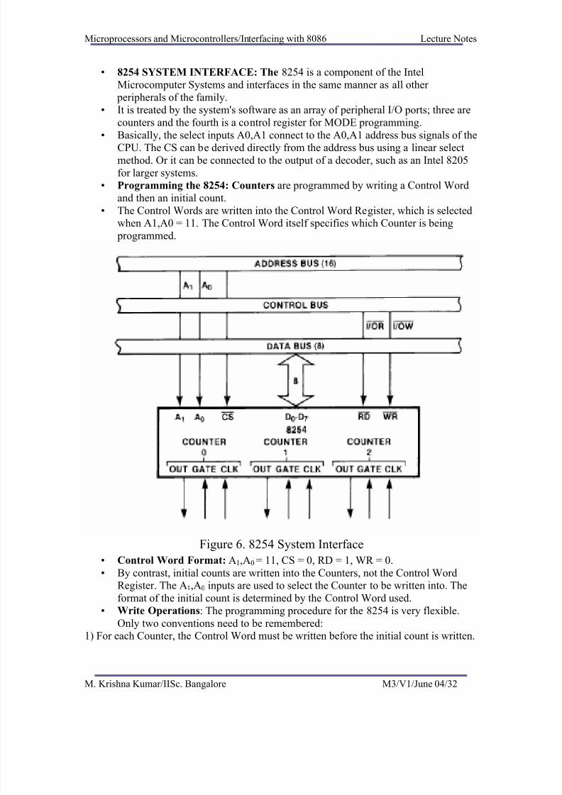
• 8254 SYSTEM INTERFACE: The 8254 is a component of the Intel
Microcomputer Systems and interfaces in the same manner as all other
peripherals of the family.• It is treated by the system's software as an array of peripheral I/O ports; three are
counters and the fourth is a control register for MODE programming.
•
Basically, the select inputs A0,A1 connect to the A0,A1 address bus signals of theCPU. The CS can be derived directly from the address bus using a linear select
method. Or it can be connected to the output of a decoder, such as an Intel 8205
for larger systems.• Programming the 8254: Counters are programmed by writing a Control Word
and then an initial count.
• The Control Words are written into the Control Word Register, which is selectedwhen A1,A0 = 11. The Control Word itself specifies which Counter is being
programmed.
Figure 6. 8254 System Interface
• Control Word Format: A1,A0 = 11, CS = 0, RD = 1, WR = 0.• By contrast, initial counts are written into the Counters, not the Control Word
Register. The A1,A0 inputs are used to select the Counter to be written into. The
format of the initial count is determined by the Control Word used.
• Write Operations: The programming procedure for the 8254 is very flexible.
Only two conventions need to be remembered:1) For each Counter, the Control Word must be written before the initial count is written.
M. Krishna Kumar/IISc. Bangalore M3/V1/June 04/32

8/14/2019 microprocessor and microcontroller module 3
http://slidepdf.com/reader/full/microprocessor-and-microcontroller-module-3 33/91
Microprocessors and Microcontrollers/Interfacing with 8086 Lecture Notes
2) The initial count must follow the count format specified in the Control Word (least
significant byte only, most significant byte only, or least significant byte and then most
significant byte).• Since the Control Word Register and the three Counters have separate addresses
(selected by the A1,A0 inputs), and each Control Word specifies the Counter it
applies to (SC0,SC1 bits), no special instruction sequence is required.• Any programming sequence that follows the conventions in Figure 7 is
acceptable.
NOTE: Don't care bits (X) should be 0 to insure compatibility with future Intel products.
Figure 7. Control Word Format
• A new initial count may be written to a Counter at any time without affecting the
Counter's programmed Mode in any way. Counting will be affected as describedin the Mode definitions. The new count must follow the programmed count
format.
• If a Counter is programmed to read/write two-byte counts, the following precaution applies: A program must not transfer control between writing the first
and second byte to another routine which also writes into that same Counter.
Otherwise, the Counter will be loaded with an incorrect count.
M. Krishna Kumar/IISc. Bangalore M3/V1/June 04/33

8/14/2019 microprocessor and microcontroller module 3
http://slidepdf.com/reader/full/microprocessor-and-microcontroller-module-3 34/91
Microprocessors and Microcontrollers/Interfacing with 8086 Lecture Notes
Figure 8. A Few Possible Programming Sequences
• Read Operations: It is often desirable to read the value of a Counter withoutdisturbing the count in progress. This is easily done in the 8254.
• There are three possible methods for reading the counters: a simple read
operation, the Counter Latch Command, and the Read-Back Command.• Each is explained below. The first method is to perform a simple read operation.
To read the Counter, which is selected with the A1, A0 inputs, the CLK input of the selected Counter must be inhibited by using either the GATE input or externallogic.
• Otherwise, the count may be in the process of changing when it is read, giving an
undefined result.• COUNTER LATCH COMMAND: The second method uses the ``Counter
Latch Command''.
• Like a Control Word, this command is written to the Control Word Register,
which is selected when A1,A0 = 11. Also like a Control Word, the SC0, SC1 bitsselect one of the three Counters, but two other bits, D5 and D4, distinguish this
command from a Control Word.
• The selected Counter's output latch (OL) latches the count at the time the Counter Latch Command is received. This count is held in the latch until it is read by the
CPU (or until the Counter is reprogrammed).
M. Krishna Kumar/IISc. Bangalore M3/V1/June 04/34

8/14/2019 microprocessor and microcontroller module 3
http://slidepdf.com/reader/full/microprocessor-and-microcontroller-module-3 35/91
Microprocessors and Microcontrollers/Interfacing with 8086 Lecture Notes
Figure 9. Counter Latching Command Format
• The count is then unlatched automatically and the OL returns to ``following'' thecounting element (CE).
• This allows reading the contents of the Counters ``on the fly'' without affecting
counting in progress.• Multiple Counter Latch Commands may be used to latch more than one Counter.
Each latched Counter's OL holds its count until it is read.
• Counter Latch Commands do not affect the programmed Mode of the Counter in
any way.• If a Counter is latched and then, some time later, latched again before the count is
read, the second Counter Latch Command is ignored. The count read will be thecount at the time the first Counter Latch Command was issued.
• With either method, the count must be read according to the programmed format;
specifically, if the Counter is programmed for two byte counts, two bytes must be
read. The two bytes do not have to be read one right after the other, read or writeor programming operations of other Counters may be inserted between them.
• Another feature of the 8254 is that reads and writes of the same Counter may be
interleaved.
M. Krishna Kumar/IISc. Bangalore M3/V1/June 04/35

8/14/2019 microprocessor and microcontroller module 3
http://slidepdf.com/reader/full/microprocessor-and-microcontroller-module-3 36/91
Microprocessors and Microcontrollers/Interfacing with 8086 Lecture Notes
• Example: If the Counter is programmed for two byte counts, the following
sequence is valid.
1) Read least significant byte.2) Write new least significant byte.
3) Read most significant byte.
4) Write new most significant byte.• If a Counter is programmed to read/write two-byte counts, the following
precaution applies: A program must not transfer control between reading the first
and second byte to another routine which also reads from that same Counter.Otherwise, an incorrect count will be read.
• READ-BACK COMMAND: The third method uses the Read-Back Command.
This command allows the user to check the count value, programmed Mode, andcurrent states of the OUT pin and Null Count flag of the selected counter (s).
• The command is written into the Control Word Register and has the format shown
in Figure 10. The command applies to the counters selected by setting their
corresponding bits D3, D2, D1 = 1.
•
The read-back command may be used to latch multiple counter output latches(OL) by setting the COUNT bit D5 = 0 and selecting the desired counter (s). This
single command is functionally equivalent to several counter latch commands,one for each counter latched.
• Each counter's latched count is held until it is read (or the counter is
reprogrammed).• The counter is automatically unlatched when read, but other counters remain
latched until they are read. If multiple count read-back commands are issued tothe same counter without reading the count, all but the first are ignored; i.e., thecount which will be read is the count at the time the first read-back command was
issued.
• The read-back command may also be used to latch status information of selectedcounter (s) by setting STATUS bit D4 = 0. Status must be latched to be read;
status of a counter is accessed by a read from that counter.
• The counter status format is shown in Figure 11.
M. Krishna Kumar/IISc. Bangalore M3/V1/June 04/36

8/14/2019 microprocessor and microcontroller module 3
http://slidepdf.com/reader/full/microprocessor-and-microcontroller-module-3 37/91
Microprocessors and Microcontrollers/Interfacing with 8086 Lecture Notes
• Bits D5 through D0 contain the counter's programmed Mode exactly as written in
the last Mode Control Word. OUTPUT bit D7 contains the current state of the
OUT pin.• This allows the user to monitor the counter's output via software, possibly
eliminating some hardware from a system. NULL COUNT bit D6 indicates when
the last count written to the counter register (CR) has been loaded into thecounting element (CE).
• The exact time this happens depends on the Mode of the counter and is described
in the Mode Definitions, but until the count is loaded into the counting element(CE), it can't be read from the counter.
Figure 11. Status Byte
• If the count is latched or read before this time, the count value will not reflect thenew count just written. The operation of Null Count is shown in Figure 12.
• If multiple status latch operations of the counter (s) are performed without reading
the status, all but the first are ignored; i.e., the status that will be read is the status
of the counter at the time the first status read-back command was issued.• Both count and status of the selected counter (s) may be latched simultaneously
by setting both COUNT and STATUS bits D5,D4 = 0. This is functionally the
same as issuing two separate read-back commands at once, and the abovediscussions apply here also.
M. Krishna Kumar/IISc. Bangalore M3/V1/June 04/37

8/14/2019 microprocessor and microcontroller module 3
http://slidepdf.com/reader/full/microprocessor-and-microcontroller-module-3 38/91
Microprocessors and Microcontrollers/Interfacing with 8086 Lecture Notes
Figure 12. Null Count Operation
• Specifically, if multiple count and/or status read-back commands are issued to thesame counter (s) without any intervening reads, all but the first are ignored. This
is illustrated in Figure 13.
• If both count and status of a counter are latched, the first read operation of that
counter will return latched status, regardless of which was latched first. The nextone or two reads (depending on whether the counter is programmed for one or
two type counts) return latched count. Subsequent reads return unlatched count.
M. Krishna Kumar/IISc. Bangalore M3/V1/June 04/38

8/14/2019 microprocessor and microcontroller module 3
http://slidepdf.com/reader/full/microprocessor-and-microcontroller-module-3 39/91
Microprocessors and Microcontrollers/Interfacing with 8086 Lecture Notes
Figure 13. Read-Back Command Example
Figure 14. Read/Write Operations Summary
• Mode Definitions :The following are defined for use in describing the operationof the 8254.
• CLK Pulse: A rising edge, then a falling edge, in that order, of a Counter's CLK
input.
• Trigger: A rising edge of a Counter's GATE input.
M. Krishna Kumar/IISc. Bangalore M3/V1/June 04/39

8/14/2019 microprocessor and microcontroller module 3
http://slidepdf.com/reader/full/microprocessor-and-microcontroller-module-3 40/91
Microprocessors and Microcontrollers/Interfacing with 8086 Lecture Notes
• Counter loading: The transfer of a count from the CR to the CE (refer to the
``Functional Description'').
• MODE 0: INTERRUPT ON TERMINAL COUNT :• Mode 0 is typically used for event counting. After the Control Word is written,
OUT is initially low, and will remain low until the Counter reaches zero.
•
OUT then goes high and remains high until a new count or a new Mode 0 ControlWord is written into the Counter.
• GATE = 1 enables counting; GATE = 0 disables counting. GATE has no effect on
OUT.• After the Control Word and initial count are written to a Counter, the initial count
will be loaded on the next CLK pulse. This CLK pulse does not decrement the
count, so for an initial count of N, OUT does not go high until N a 1 CLK pulsesafter the initial count is written.
• If a new count is written to the Counter, it will be loaded on the next CLK pulse
and counting will continue from the new count. If a two-byte count is written, the
following happens:
1) Writing the first byte disables counting. OUT is set low immediately (no clock pulse required).
2) Writing the second byte allows the new count to be loaded on the next CLK pulse.• This allows the counting sequence to be synchronized by software. Again, OUT
does not go high until Na1 CLK pulses after the new count of N is written.
• If an initial count is written while GATE e 0, it will still be loaded on the nextCLK pulse. When GATE goes high, OUT will go high N CLK pulses later; no
CLK pulse is needed to load the Counter as this has already been done.
M. Krishna Kumar/IISc. Bangalore M3/V1/June 04/40

8/14/2019 microprocessor and microcontroller module 3
http://slidepdf.com/reader/full/microprocessor-and-microcontroller-module-3 41/91
Microprocessors and Microcontrollers/Interfacing with 8086 Lecture Notes
Fi ure 15. Mode 0
Note:
1. Counters are programmed for binary (not BCD) counting and for reading/writing
least significant byte (LSB) only.
2. The counter is always selected (CS always low).
3. CW stands for ``Control Word''; CW = 10 means a control word of 10 HEX iswritten to the counter.
4. LSB stands for ``Least Significant Byte'' of count.
5. Numbers below diagrams are count values. The lower number is the leastsignificant byte. The upper number is the most significant byte. Since the counter is
programmed to read/write LSB only, the most significant byte cannot be
read. N stands for an undefined count. Vertical lines show transitions between countvalues.
• MODE 1: HARDWARE RETRIGGERABLE ONE-SHOT : OUT will be
initially high.
• OUT will go low on the CLK pulse following a trigger to begin the one-shot
pulse, and will remain low until the Counter reaches zero.• OUT will then go high and remain high until the CLK pulse after the next trigger.
• After writing the Control Word and initial count, the Counter is armed. A trigger results in loading the Counter and setting OUT low on the next CLK pulse, thus
starting the one-shot pulse. An initial count of N will result in a one-shot pulse N
CLK cycles in duration.
M. Krishna Kumar/IISc. Bangalore M3/V1/June 04/41

8/14/2019 microprocessor and microcontroller module 3
http://slidepdf.com/reader/full/microprocessor-and-microcontroller-module-3 42/91
Microprocessors and Microcontrollers/Interfacing with 8086 Lecture Notes
• The one-shot is retriggerable, hence OUT will remain low for N CLK pulses after
any trigger. The one-shot pulse can be repeated without rewriting the same count
into the counter. GATE has no effect on OUT.• If a new count is written to the Counter during a oneshot pulse, the current one-
shot is not affected unless the counter is retriggered. In that case, the Counter is
loaded with the new count and the oneshot pulse continues until the new countexpires.
Figure 16. Mode 1• MODE 2: RATE GENERATOR: This Mode functions like a divide-by-N
counter. It is typically used to generate a Real Time Clock interrupt.• OUT will initially be high. When the initial count has decremented to 1, OUT
goes low for one CLK pulse. OUT then goes high again, the Counter reloads the
initial count and the process is repeated.• Mode 2 is periodic, the same sequence is repeated indefinitely. For an initial
count of N, the sequence repeats every N CLK cycles.
• GATE = 1 enables counting; GATE = 0 disables counting. If GATE goes lowduring an output pulse, OUT is set high immediately.
• A trigger reloads the Counter with the initial count on the next CLK pulse, OUT
goes low N CLK pulses after the trigger. Thus the GATE input can be used tosynchronize the Counter.
• After writing a Control Word and initial count, the Counter will be loaded on the
next CLK pulse. OUT goes low N CLK Pulses after the initial count is written.
• This allows the Counter to be synchronized by software also. Writing a new countwhile counting does not affect the current counting sequence.
M. Krishna Kumar/IISc. Bangalore M3/V1/June 04/42

8/14/2019 microprocessor and microcontroller module 3
http://slidepdf.com/reader/full/microprocessor-and-microcontroller-module-3 43/91
Microprocessors and Microcontrollers/Interfacing with 8086 Lecture Notes
• If a trigger is received after writing a new count but before the end of the current
period, the Counter will be loaded with the new count on the next CLK pulse and
counting will continue from the new count.• Otherwise, the new count will be loaded at the end of the current counting cycle.
In mode 2, a COUNT of 1 is illegal.
•
MODE 3: SQUARE WAVE MODE :Mode 3 is typically used for Baud rategeneration. Mode 3 is similar to Mode 2 except for the duty cycle of OUT. OUT
will initially be high.
Figure 17. Mode 2
• When half the initial count has expired, OUT goes low for the remainder of thecount. Mode 3 is periodic; the sequence above is repeated indefinitely.
• An initial count of N results in a square wave with a period of N CLK cycles.
GATE = 1 enables counting; GATE = 0 disables counting. If GATE goes lowwhile OUT is low, OUT is set high immediately; no CLK pulse is required.
• A trigger reloads the Counter with the initial count on the next CLK pulse. Thus
the GATE input can be used to synchronize the Counter.
•
After writing a Control Word and initial count, the Counter will be loaded on thenext CLK pulse. This allows the Counter to be synchronized by software also.
• Writing a new count while counting does not affect the current counting
sequence. If a trigger is received after writing a new count but before the end of the current half-cycle of the square wave, the Counter will be loaded with the new
count on the next CLK pulse and counting will continue from the new count.
Otherwise, the new count will be loaded at the end of the current half-cycle.
M. Krishna Kumar/IISc. Bangalore M3/V1/June 04/43

8/14/2019 microprocessor and microcontroller module 3
http://slidepdf.com/reader/full/microprocessor-and-microcontroller-module-3 44/91
Microprocessors and Microcontrollers/Interfacing with 8086 Lecture Notes
• Mode 3:Even counts: OUT is initially high. The initial count is loaded on one
CLK pulse and then is decremented by two on succeeding CLK pulses.
• When the count expires OUT changes value and the Counter is reloaded with theinitial count. The above process is repeated indefinitely.
• Odd counts: OUT is initially high. The initial count minus one (an even number)
is loaded on one CLK pulse and then is decremented by two on succeeding CLK pulses.
Figure 18. Mode 3
• One CLK pulse after the count expires, OUT goes low and the Counter isreloaded with the initial count minus one.
• Succeeding CLK pulses decrement the count by two.
• When the count expires, OUT goes high again and the Counter is reloaded withthe initial count minus one. The above process is repeated indefinitely.
• So for odd counts, OUT will be high for (N - 1)/2 counts and low for (N - 1)/2
counts.
• MODE 4: SOFTWARE TRIGGERED STROBE :• OUT will be initially high. When the initial count expires, OUT will go low for
one CLK pulse and then go high again. The counting sequence is ``triggered'‘ bywriting the initial count.
• GATE = 1 enables counting; GATE = 0 disables counting. GATE has no effect on
OUT. After writing a Control Word and initial count, the Counter will be loaded
on the next CLK pulse.
M. Krishna Kumar/IISc. Bangalore M3/V1/June 04/44
8/14/2019 microprocessor and microcontroller module 3
http://slidepdf.com/reader/full/microprocessor-and-microcontroller-module-3 45/91
Microprocessors and Microcontrollers/Interfacing with 8086 Lecture Notes
• This CLK pulse does not decrement the count, so for an initial count of N, OUT
does not strobe low until N + 1 CLK pulses after the initial count is written.
• If a new count is written during counting, it will be loaded on the next CLK pulseand counting will continue from the new count. If a two-byte count is written, the
following happens:
1) Writing the first byte has no effect on counting.2) Writing the second byte allows the new count to be loaded on the next CLK pulse.
• This allows the sequence to be ``retriggered'' by software. OUT strobes low N a 1
CLK pulses after the new count of N is written.
Figure 19. Mode 4
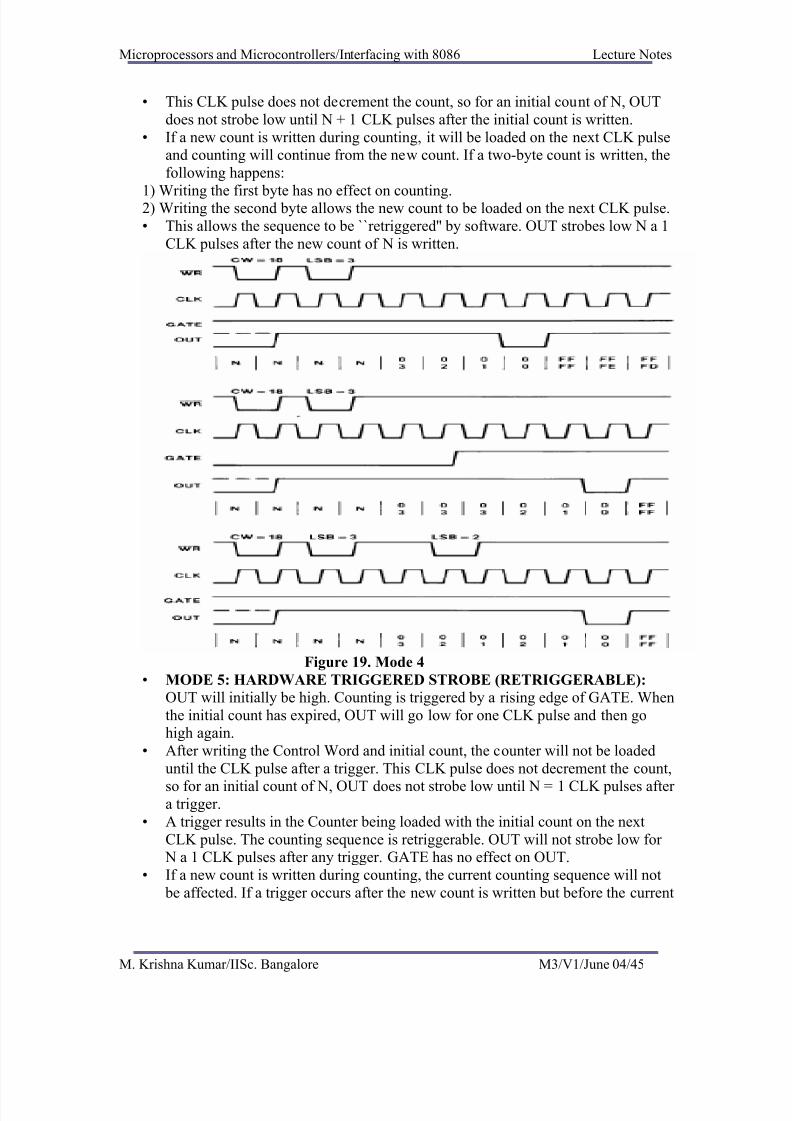
• MODE 5: HARDWARE TRIGGERED STROBE (RETRIGGERABLE):
OUT will initially be high. Counting is triggered by a rising edge of GATE. When
the initial count has expired, OUT will go low for one CLK pulse and then gohigh again.
• After writing the Control Word and initial count, the counter will not be loaded
until the CLK pulse after a trigger. This CLK pulse does not decrement the count,
so for an initial count of N, OUT does not strobe low until N = 1 CLK pulses after a trigger.
• A trigger results in the Counter being loaded with the initial count on the next
CLK pulse. The counting sequence is retriggerable. OUT will not strobe low for N a 1 CLK pulses after any trigger. GATE has no effect on OUT.
• If a new count is written during counting, the current counting sequence will not
be affected. If a trigger occurs after the new count is written but before the current
M. Krishna Kumar/IISc. Bangalore M3/V1/June 04/45

8/14/2019 microprocessor and microcontroller module 3
http://slidepdf.com/reader/full/microprocessor-and-microcontroller-module-3 46/91
Microprocessors and Microcontrollers/Interfacing with 8086 Lecture Notes
count expires, the Counter will be loaded with the new count on the next CLK
pulse and counting will continue from there.
Figure 20. Mode 5
• Operation Common to All Modes:
• PROGRAMMING: When a Control Word is written to a Counter, all Control
Logic is immediately reset and OUT goes to a known initial state; no CLK pulsesare required for this.
• GATE: The GATE input is always sampled on the rising edge of CLK. In Modes
0, 2, 3, and 4 the GATE input is level sensitive, and the logic level is sampled on
the rising edge of CLK. In Modes 1, 2, 3, and 5 the GATE input is rising-edgesensitive.
• In these Modes, a rising edge of GATE (trigger) sets an edge-sensitive flip-flop in
the Counter. This flip-flop is then sampled on the next rising edge of CLK; theflip-flop is reset immediately after it is sampled. In this way, a trigger will be
detected no matter when it occurs-a high logic level does not have to be
maintained until the next rising edge of CLK.
• Note that in Modes 2 and 3, the GATE input is both edge- and level-sensitive. InModes 2 and 3, if a CLK source other than the system clock is used, GATE
should be pulsed immediately following WR of a new count value.
M. Krishna Kumar/IISc. Bangalore M3/V1/June 04/46

8/14/2019 microprocessor and microcontroller module 3
http://slidepdf.com/reader/full/microprocessor-and-microcontroller-module-3 47/91
Microprocessors and Microcontrollers/Interfacing with 8086 Lecture Notes
Figure 21. Gate Pin Operations Summary
• COUNTER : New counts are loaded and Counters are decremented on the falling
edge of CLK.• The largest possible initial count is 0, this is equivalent to 216 for binary counting
and 104 for BCD counting. The Counter does not stop when it reaches zero.• In Modes 0, 1, 4, and 5 the Counter ``wraps around'' to the highest count, either
FFFF hex for binary counting or 9999 for BCD counting, and continues counting.
• Modes 2 and 3 are periodic; the Counter reloads itself with the initial count andcontinues counting from there.
M. Krishna Kumar/IISc. Bangalore M3/V1/June 04/47

8/14/2019 microprocessor and microcontroller module 3
http://slidepdf.com/reader/full/microprocessor-and-microcontroller-module-3 48/91
Microprocessors and Microcontrollers/Interfacing with 8086 Lecture Notes
NOTE: 0 is equivalent to 216
for binary counting and 104
for BCD counting.
Figure 22. Minimum and Maximum Initial Counts
8279• While studying 8255, we have explained the use of 8255 in interfacing keyboards
and displays with 8086. The disadvantages of this method of interfacing keyboard
and display with 8086 is that the processor has to refresh the display and check
the status of the keyboard periodically using polling technique. Thus aconsiderable amount of CPU time is wasted, reducing the system operating speed.
• Intel’s 8279 is a general purpose keyboard display controller that simultaneously
drives the display of a system and interfaces a keyboard with the CPU, leaving it
free for its routine task.
Architecture and Signal Descriptions of 8279• The keyboard display controller chip 8279 provides:a) a set of four scan lines and eight return lines for interfacing keyboards
b) A set of eight output lines for interfacing display.
• Fig shows the functional block diagram of 8279 followed by its brief description.
• I/O Control and Data Buffers : The I/O control section controls the flow of data
to/from the 8279. The data buffers interface the external bus of the system with
internal bus of 8279.
• The I/O section is enabled only if CS is low. The pins A0, RD and WR select thecommand, status or data read/write operations carried out by the CPU with 8279.
• Control and Timing Register and Timing Control : These registers store the
keyboard and display modes and other operating conditions programmed by CPU.The registers are written with A0=1 and WR=0. The Timing and control unit
controls the basic timings for the operation of the circuit. Scan counter divide
down the operating frequency of 8279 to derive scan keyboard and scan displayfrequencies.
• Scan Counter : The scan counter has two modes to scan the key matrix and
refresh the display. In the encoded mode, the counter provides binary count that is
to be externally decoded to provide the scan lines for keyboard and display (Four
M. Krishna Kumar/IISc. Bangalore M3/V1/June 04/48

8/14/2019 microprocessor and microcontroller module 3
http://slidepdf.com/reader/full/microprocessor-and-microcontroller-module-3 49/91
Microprocessors and Microcontrollers/Interfacing with 8086 Lecture Notes
externally decoded scan lines may drive upto 16 displays). In the decode scan
mode, the counter internally decodes the least significant 2 bits and provides a
decoded 1 out of 4 scan on SL0-SL3(Four internally decoded scan lines may driveupto 4 displays). The keyboard and display both are in the same mode at a time.
• Return Buffers and Keyboard Debounce and Control: This section for a key
closure row wise. If a key closer is detected, the keyboard debounce unitdebounces the key entry (i.e. wait for 10 ms). After the debounce period, if the
key continues to be detected. The code of key is directly transferred to the sensor
RAM along with SHIFT and CONTROL key status.• FIFO/Sensor RAM and Status Logic: In keyboard or strobed input mode, this
block acts as 8-byte first-in-first-out (FIFO) RAM. Each key code of the pressed
key is entered in the order of the entry and in the mean time read by the CPU, tillthe RAM become empty.
• The status logic generates an interrupt after each FIFO read operation till the
FIFO is empty. In scanned sensor matrix mode, this unit acts as sensor RAM.
Each row of the sensor RAM is loaded with the status of the corresponding row of
sensors in the matrix. If a sensor changes its state, the IRQ line goes high tointerrupt the CPU.
• Display Address Registers and Display RAM : The display address register holds the address of the word currently being written or read by the CPU to or
from the display RAM. The contents of the registers are automatically updated by
8279 to accept the next data entry by CPU.
CS A0
8279 Internal Architecture
Return
DB0-DB7
DATA
BUFFERS
I/O
CONTROL
INTERNAL 8 BIT DATA BUS
FIFO/SENSOR
RAM STATUS
RD WR
R
E
SDISPLAY
ADDRESS
REGISTERS
16*8
DISPLAY
RAM
CONTROL
AND
TIMING
REGISTERS
CLK KEYBOARD
DEBOUNCE
AND
CONTROL
8*8 FIFO/
SENSOR
RAM
TIMING
AND
CONTROLUNIT
DISPLAY
REGISTERS
SCAN
COUNTER
CNTL/
STB
BD RL0 – RL7
SHIFT
OUT A0-A3
OUT B0-B3
SL0 – SL3
M. Krishna Kumar/IISc. Bangalore M3/V1/June 04/49

8/14/2019 microprocessor and microcontroller module 3
http://slidepdf.com/reader/full/microprocessor-and-microcontroller-module-3 50/91
Microprocessors and Microcontrollers/Interfacing with 8086 Lecture Notes
RL2 Vcc1 40
8279
2
3
45
6
7
8
9
10
1112
13
14
15
16
17
1819
20
39
38
3736
35
34
33
32
31
3029
28
27
26
25
24
2322
21
RL3 RL1
RL0CLK
CNTL/STBIRQSHIFTRL4
SL3RL5
SL2RL6
SL1RL7
RESET SL0
RD OUT B0
WR OUT B1
DB0 OUT B2
DB1 OUT B3
DB2 OUT A0
DB3 OUT A1
DB4 OUT A2
DB5 OUT A3
DB6 BDCSDB7
Vss A0
8279 Pin Configuration
M. Krishna Kumar/IISc. Bangalore M3/V1/June 04/50
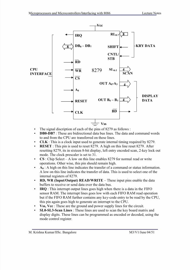
8/14/2019 microprocessor and microcontroller module 3
http://slidepdf.com/reader/full/microprocessor-and-microcontroller-module-3 51/91
Microprocessors and Microcontrollers/Interfacing with 8086 Lecture Notes
• The signal discription of each of the pins of 8279 as follows :
• DB0-DB7 : These are bidirectional data bus lines. The data and command words
to and from the CPU are transferred on these lines.
• CLK : This is a clock input used to generate internal timing required by 8279.• RESET : This pin is used to reset 8279. A high on this line reset 8279. After
resetting 8279, its in sixteen 8-bit display, left entry encoded scan, 2-key lock outmode. The clock prescaler is set to 31.
• CS : Chip Select – A low on this line enables 8279 for normal read or write
operations. Other wise, this pin should remain high.• A0 : A high on this line indicates the transfer of a command or status information.
A low on this line indicates the transfer of data. This is used to select one of the
internal registers of 8279.• RD, WR (Input/Output) READ/WRITE – These input pins enable the data
buffers to receive or send data over the data bus.
• IRQ : This interrupt output lines goes high when there is a data in the FIFOsensor RAM. The interrupt lines goes low with each FIFO RAM read operation but if the FIFO RAM further contains any key-code entry to be read by the CPU,
this pin again goes high to generate an interrupt to the CPU.• Vss, Vcc : These are the ground and power supply lines for the circuit.
• SL0-SL3-Scan Lines : These lines are used to scan the key board matrix and
display digits. These lines can be programmed as encoded or decoded, using themode control register.
Vss
Vcc
RL0-7 8IRQ
BD
4
KRY DATASHIFT
CLK
RESET
A0
CS
WR
RD
DB0 – DB78
CNTL/
STB
SL0-3 4SCAN
OUT A0-A3
OUT B0 – B3
4
DISPLAY
DATA
CPU
INTERFACE8279
M. Krishna Kumar/IISc. Bangalore M3/V1/June 04/51

8/14/2019 microprocessor and microcontroller module 3
http://slidepdf.com/reader/full/microprocessor-and-microcontroller-module-3 52/91

8/14/2019 microprocessor and microcontroller module 3
http://slidepdf.com/reader/full/microprocessor-and-microcontroller-module-3 53/91

8/14/2019 microprocessor and microcontroller module 3
http://slidepdf.com/reader/full/microprocessor-and-microcontroller-module-3 54/91
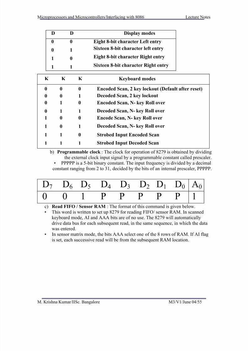
8/14/2019 microprocessor and microcontroller module 3
http://slidepdf.com/reader/full/microprocessor-and-microcontroller-module-3 55/91
Microprocessors and Microcontrollers/Interfacing with 8086 Lecture Notes
b) Programmable clock : The clock for operation of 8279 is obtained by dividing
the external clock input signal by a programmable constant called prescaler.
D D Display modes
Eight 8-bit character Left entry0 0
Sixteen 8-bit character left entry0 1
Eight 8-bit character Right entry1 0
Sixteen 8-bit character Right entry1 1
K K K Keyboard modes
0 0 0 Encoded Scan, 2 key lockout (Default after reset)
Decoded Scan, 2 key lockout0 0 1
0 1 0 Encoded Scan, N- key Roll over
Decoded Scan, N- key Roll over0 1 1
1 0 0 Encode Scan, N- key Roll over
Decoded Scan, N- key Roll over1 0 1
1 1 0 Strobed Input Encoded Scan
Strobed Input Decoded Scan1 1 1
• PPPPP is a 5-bit binary constant. The input frequency is divided by a decimal
constant ranging from 2 to 31, decided by the bits of an internal prescaler, PPPPP.
c) Read FIFO / Sensor RAM : The format of this command is given below.
D7 D6 D5 D4 D3 D2 D1 D0 A0
• This word is written to set up 8279 for reading FIFO/ sensor RAM. In scanned
keyboard mode, AI and AAA bits are of no use. The 8279 will automatically
drive data bus for each subsequent read, in the same sequence, in which the datawas entered.
• In sensor matrix mode, the bits AAA select one of the 8 rows of RAM. If AI flag
is set, each successive read will be from the subsequent RAM location.
0 0 1 P P P P P 1
M. Krishna Kumar/IISc. Bangalore M3/V1/June 04/55
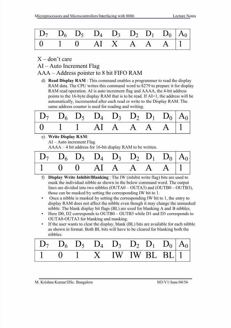
8/14/2019 microprocessor and microcontroller module 3
http://slidepdf.com/reader/full/microprocessor-and-microcontroller-module-3 56/91
Microprocessors and Microcontrollers/Interfacing with 8086 Lecture Notes
D7 D6 D5 D4 D3 D2 D1 D0 A0
0 1 0 AI X A A A 1
X – don’t careAI – Auto Increment Flag
AAA – Address pointer to 8 bit FIFO RAM
d) Read Display RAM : This command enables a programmer to read the display
RAM data. The CPU writes this command word to 8279 to prepare it for displayRAM read operation. AI is auto increment flag and AAAA, the 4-bit address
points to the 16-byte display RAM that is to be read. If AI=1, the address will be
automatically, incremented after each read or write to the Display RAM. Thesame address counter is used for reading and writing.
e) Write Display RAM:
D7 D6 D5 D4 D3 D2 D1 D0 A0
AI – Auto increment Flag.AAAA – 4 bit address for 16-bit display RAM to be written.
f) Display Write Inhibit/Blanking : The IW (inhibit write flag) bits are used to
mask the individual nibble as shown in the below command word. The outputlines are divided into two nibbles (OUTA0 – OUTA3) and (OUTB0 – OUTB3),
those can be masked by setting the corresponding IW bit to 1.
• Once a nibble is masked by setting the corresponding IW bit to 1, the entry to
display RAM does not affect the nibble even though it may change the unmaskednibble. The blank display bit flags (BL) are used for blanking A and B nibbles.
• Here D0, D2 corresponds to OUTB0 – OUTB3 while D1 and D3 corresponds to
OUTA0-OUTA3 for blanking and masking.• If the user wants to clear the display, blank (BL) bits are available for each nibble
as shown in format. Both BL bits will have to be cleared for blanking both thenibbles.
0 1 1 AI A A A A 1
D7 D6 D5 D4 D3 D2 D1 D0 A0
1 0 0 AI A A A A 1
D7 D6 D5 D4 D3 D2 D1 D0 A0
1 0 1 X IW IW BL BL 1
M. Krishna Kumar/IISc. Bangalore M3/V1/June 04/56

8/14/2019 microprocessor and microcontroller module 3
http://slidepdf.com/reader/full/microprocessor-and-microcontroller-module-3 57/91
Microprocessors and Microcontrollers/Interfacing with 8086 Lecture Notes
g) Clear Display RAM : The CD2, CD1, CD0 is a selectable blanking code to clear
all the rows of the display RAM as given below. The characters A and B
represents the output nibbles.• CD2 must be 1 for enabling the clear display command. If CD2 = 0, the clear
display command is invoked by setting CA=1 and maintaining CD1, CD0 bits
exactly same as above. If CF=1, FIFO status is cleared and IRQ line is pulleddown.
• Also the sensor RAM pointer is set to row 0. if CA=1, this combines the effect of
CD and CF bits. Here, CA represents Clear All and CF as Clear FIFO RAM.
D7 D6 D5 D4 D3 D2 D1 D0 A0
h) End Interrupt / Error mode Set : For the sensor matrix mode, this command
lowers the IRQ line and enables further writing into the RAM. Otherwise, if a
change in sensor value is detected, IRQ goes high that inhibits writing in thesensor RAM.
• For N-Key roll over mode, if the E bit is programmed to be ‘1’, the 8279 operates
in special Error mode. Details of this mode are described in scanned keyboard
special error mode. X- don’t care.
1 1 0 CD2 CD1 CD0 CF CA 1
CD2 CD1 CD0
1 0 X
1 1 01 1 1All zeros (x don’t care) AB=00
A3-A0 =2 (0010) and B3-B0=00 (0000)
All ones (AB =FF), i.e. clear RAM
D7 D6 D5 D4 D3 D2 D1 D0 A0
1 1 1 E X X X X 1
M. Krishna Kumar/IISc. Bangalore M3/V1/June 04/57

8/14/2019 microprocessor and microcontroller module 3
http://slidepdf.com/reader/full/microprocessor-and-microcontroller-module-3 58/91
Microprocessors and Microcontrollers/Interfacing with 8086 Lecture Notes
8259A• If we are working with an 8086, we have a problem here because the 8086 has
only two interrupt inputs, NMI and INTR.
• If we save NMI for a power failure interrupt, this leaves only one interrupt for all
the other applications. For applications where we have interrupts from multiplesource, we use an external device called a priority interrupt controller (PIC) to
the interrupt signals into a single interrupt input on the processor.
Architecture and Signal Descriptions of 8259A• The architectural block diagram of 8259A is shown in fig1. The functional
explication of each block is given in the following text in brief.
• Interrupt Request Register (RR): The interrupts at IRQ input lines are handled by Interrupt Request internally. IRR stores all the interrupt request in it in order to
serve them one by one on the priority basis.
• In-Service Register (ISR): This stores all the interrupt requests those are beingserved, i.e. ISR keeps a track of the requests being served.
8
4
4
8086
8279
Key
board
ShiftINT28259
Interru
pt
controll
er
INTR Control
Return
lines
8 columns8 rows
8
AD0-AD15
A16-A19
8282 (3)
Address
latch
5VA0L-A19L 3-8 decoderVDDRL0-
INT
RD
WR PCLK
(from 8284)
Address
decoder
A0L
A1L-A3L
4-16
AddresDisplay
characte
r data
Blank
display
BD
A0-3B0-3CLK A0
CS
Reset
IOWIOR
D0-7
S0-3
Vs0V
Scan
lines
3
Data 4
16
M. Krishna Kumar/IISc. Bangalore M3/V1/June 04/58

8/14/2019 microprocessor and microcontroller module 3
http://slidepdf.com/reader/full/microprocessor-and-microcontroller-module-3 59/91
Microprocessors and Microcontrollers/Interfacing with 8086 Lecture Notes
• Priority Resolver : This unit determines the priorities of the interrupt requests
appearing simultaneously. The highest priority is selected and stored into thecorresponding bit of ISR during INTA pulse. The IR0 has the highest priority
while the IR7 has the lowest one, normally in fixed priority mode. The priorities
however may be altered by programming the 8259A in rotating priority mode.• Interrupt Mask Register (IMR) : This register stores the bits required to mask
the interrupt inputs. IMR operates on IRR at the direction of the Priority Resolver. • Interrupt Control Logic: This block manages the interrupt and interrupt
acknowledge signals to be sent to the CPU for serving one of the eight interrupt
requests. This also accepts the interrupt acknowledge (INTA) signal from CPU
that causes the 8259A to release vector address on to the data bus.• Data Bus Buffer : This tristate bidirectional buffer interfaces internal 8259A bus
to the microprocessor system data bus. Control words, status and vector
information pass through data buffer during read or write operations.
• Read/Write Control Logic: This circuit accepts and decodes commands from theCPU. This block also allows the status of the 8259A to be transferred on to the
data bus.
• Cascade Buffer/Comparator: This block stores and compares the ID’s all the8259A used in system. The three I/O pins CASO-2 are outputs when the 8259A is
used as a master. The same pins act as inputs when the 8259A is in slave mode.
The 8259A in master mode sends the ID of the interrupting slave device on theselines. The slave thus selected, will send its preprogrammed vector address on the
data bus during the next INTA pulse.
• CS: This is an active-low chip select signal for enabling RD and WR operations
of 8259A. INTA function is independent of CS.
Fig:1 8259A Block Diagram
INTA INT
D0-D7 Control LogicData Bus
Buffer
RD
Interrupt Mask RegisterIMR
IN Service
Register
ISR
Priority
Resolver
Interrupt
Request
Register
IRR
Read/
Write
Logic
Cascade
Buffer/
Comparator
WR
A0
CS
IR 0
IR 1
IR 7CAS0
CAS1
CAS2
SP / EN
Internal Bus
M. Krishna Kumar/IISc. Bangalore M3/V1/June 04/59

8/14/2019 microprocessor and microcontroller module 3
http://slidepdf.com/reader/full/microprocessor-and-microcontroller-module-3 60/91
Microprocessors and Microcontrollers/Interfacing with 8086 Lecture Notes
• WR : This pin is an active-low write enable input to 8259A. This enables it to
accept command words from CPU.
• RD : This is an active-low read enable input to 8259A. A low on this line enables8259A to release status onto the data bus of CPU.
• D0-D7 : These pins from a bidirectional data bus that carries 8-bit data either to
control word or from status word registers. This also carries interrupt vector information.
• CAS0 – CAS2 Cascade Lines : A signal 8259A provides eight vectored
interrupts. If more interrupts are required, the 8259A is used in cascade mode. Incascade mode, a master 8259A along with eight slaves 8259A can provide upto
64 vectored interrupt lines. These three lines act as select lines for addressing the
slave 8259A.• PS/EN : This pin is a dual purpose pin. When the chip is used in buffered mode, it
can be used as buffered enable to control buffer transreceivers. If this is not used
in buffered mode then the pin is used as input to designate whether the chip is
used as a master (SP =1) or slave (EN = 0).
•
INT : This pin goes high whenever a valid interrupt request is asserted. This isused to interrupt the CPU and is connected to the interrupt input of CPU.
• IR0 – IR7 (Interrupt requests) :These pins act as inputs to accept interruptrequest to the CPU. In edge triggered mode, an interrupt service is requested by
raising an IR pin from a low to a high state and holding it high until it is
acknowledged, and just by latching it to high level, if used in level triggeredmode.
M. Krishna Kumar/IISc. Bangalore M3/V1/June 04/60

8/14/2019 microprocessor and microcontroller module 3
http://slidepdf.com/reader/full/microprocessor-and-microcontroller-module-3 61/91

8/14/2019 microprocessor and microcontroller module 3
http://slidepdf.com/reader/full/microprocessor-and-microcontroller-module-3 62/91
Microprocessors and Microcontrollers/Interfacing with 8086 Lecture Notes
• If more than one interrupt requests are received at a time, all the requesting
peripherals are served one by one on priority basis.
• This method of interfacing may require additional hardware if number of peripherals to be interfaced is more than the interrupt pins available with the CPU.
Interrupt Sequence in an 8086 system
• The Interrupt sequence in an 8086-8259A system is described as follows:1. One or more IR lines are raised high that set corresponding IRR bits.
2. 8259A resolves priority and sends an INT signal to CPU.3. The CPU acknowledge with INTA pulse.
4. Upon receiving an INTA signal from the CPU, the highest priority ISR bit is set
and the corresponding IRR bit is reset. The 8259A does not drive data during this
period.5. The 8086 will initiate a second INTA pulse. During this period 8259A releases an
8-bit pointer on to a data bus from where it is read by the CPU.
6. This completes the interrupt cycle. The ISR bit is reset at the end of the secondINTA pulse if automatic end of interrupt (AEOI) mode is programmed. Otherwise
ISR bit remains set until an appropriate EOI command is issued at the end of interrupt subroutine.
Command Words of 8259A• The command words of 8259A are classified in two groups
1. Initialization command words (ICW) and2. Operation command words (OCW).
• Initialization Command Words (ICW): Before it starts functioning, the 8259A
must be initialized by writing two to four command words into the respectivecommand word registers. These are called as initialized command words.
• If A0 = 0 and D4 = 1, the control word is recognized as ICW1. It contains the
control bits for edge/level triggered mode, single/cascade mode, call address
interval and whether ICW4 is required or not.• If A0=1, the control word is recognized as ICW2. The ICW2 stores details
regarding interrupt vector addresses. The initialisation sequence of 8259A is
described in form of a flow chart in fig 3 below.• The bit functions of the ICW1 and ICW2 are self explanatory as shown in fig
below.
M. Krishna Kumar/IISc. Bangalore M3/V1/June 04/62

8/14/2019 microprocessor and microcontroller module 3
http://slidepdf.com/reader/full/microprocessor-and-microcontroller-module-3 63/91
Microprocessors and Microcontrollers/Interfacing with 8086 Lecture Notes
ICW1
ICW2
NO (SINGLE =1) A : IN CASCADE MODE ?A
YES (SINGLE =0)
ICW3
NO (IC4 =0)B B : IS ICW4 NEEDED ?
YES (IC4 = 1)
ICW4
Ready to Accept
Interrupt Request
Fig 3: Initialisation Sequence of 8259A
M. Krishna Kumar/IISc. Bangalore M3/V1/June 04/63

8/14/2019 microprocessor and microcontroller module 3
http://slidepdf.com/reader/full/microprocessor-and-microcontroller-module-3 64/91
Microprocessors and Microcontrollers/Interfacing with 8086 Lecture Notes
D5 D4 D1 D0A0 D7 D6 D3 D2
0 A7 A6 A5 1 LTIM ADI SNGL IC4
• Once ICW1 is loaded, the following initialization procedure is carried outinternally.
a. The edge sense circuit is reset, i.e. by default 8259A interrupts are edge sensitive.
b. IMR is cleared.
c. IR7 input is assigned the lowest priority.d. Slave mode address is set to 7.
e. Special mask mode is cleared and status read is set to IRR.f. If IC4 = 0, all the functions of ICW4 are set to zero. Master/Slave bit in ICW4 is
used in the buffered mode only.
g. In an 8085 based system A15-A8 of the interrupt vector address are the respective
bits of ICW2.h. In 8086 based system A15-A11 of the interrupt vector address are inserted in
place of T7 – T3 respectively and the remaining three bits A8, A9, A10 are
selected depending upon the interrupt level, i.e. from 000 to 111 for IR0 to IR7.i. ICW1 and ICW2 are compulsory command words in initialization sequence of
8259A as is evident from fig, while ICW3 and ICW4 are optional. The ICW3 isread only when there are more than one 8259A in the system, cascading is used
(SNGL=0).
j. The SNGL bit in ICW1 indicates whether the 8259A in the cascade mode or not.The ICW3 loads an 8-bit slave register. It detailed functions are as follows.
k. In master mode [ SP = 1 or in buffer mode M/S = 1 in ICW4], the 8-bit slave
register will be set bit-wise to 1 for each slave in the system as in fig 5.
D0D1D2D3D4D5D6D7A0
1 = ICW4 Needed 0= No ICW4 Needed
1 – Single 0 -
Cascaded
A7-A5 of Interruptvector address MCs
80/85 mode only
ICW1
1 – Level Triggered 0
– Edge Triggered
Call Address Interval
1 – Interval of 4 bytes
0 – Interval of 8 bytes.ICW2
1 T7 T6 T5 T4 T3 A10 A9 A8
• T7 – T3 are A3 – A0 of interrupt address
• A10 – A9, A8 – Selected according to interrupt request level.
The are not the address lines of Micro rocessor
Fi 4 : Instruction Command Words ICW1 and• A0 =1 selects ICW2
M. Krishna Kumar/IISc. Bangalore M3/V1/June 04/64

8/14/2019 microprocessor and microcontroller module 3
http://slidepdf.com/reader/full/microprocessor-and-microcontroller-module-3 65/91
Microprocessors and Microcontrollers/Interfacing with 8086 Lecture Notes
l. The requesting slave will then release the second byte of a CALL sequence. In
slave mode [ SP=0 or if BUF =1 and M/S = 0 in ICW4] bits D2 to D0 identify the
slave, i.e. 000 to 111 for slave 1 to slave 8. The slave compares the cascade inputswith these bits and if they are equal, the second byte of the CALL sequence is
released by it on the data bus.
D5 D4
Master mode ICW3
D1 D0A0 D7 D6 D3 D2
1 S7 S6 S5 S4 S3 S2 S1 S0
Sn = 1-IRn Input has a slave = 0 – IRn
Input does not have a slave
Slave mode ICW3
A0 D5 D4 D1 D0D7 D6 D3 D2
1 0 0 0 0 0 ID2 ID1 ID0
D2D1D0 – 000 to 111 for IR 0 to IR 7 or slave 1 to slave 8
• ICW4: The use of this command word depends on the IC4 bit of ICW1. If IC4=1,IC4 is used, otherwise it is neglected. The bit functions of ICW4 are described as
follow:
• SFNM: If BUF = 1, the buffered mode is selected. In the buffered mode, SP/ENacts as enable output and the master/slave is determined using the M/S bit of
ICW4.
• M/S
: If M/S = 1, 8259A is a master. If M/S =0, 8259A is slave. If BUF = 0, M/Sis to be neglected.• AEOI: If AEOI = 1, the automatic end of interrupt mode is selected.
• µPM : If the µPM bit is 0, the Mcs-85 system operation is selected and if µPM=1,
8086/88 operation is selected.• Operation Command Words: Once 8259A is initialized using the previously
discussed command words for initialisation, it is ready for its normal function, i.e.
for accepting the interrupts but 8259A has its own way of handling the received
Fig : ICW3 in Master and Slave Mode, ICW4 Bit Functions
D0D1D2D3D4D5
ICW4
A0 D7 D6
1 0 0 0 SFNM BUF M/S AEOI µPM
M. Krishna Kumar/IISc. Bangalore M3/V1/June 04/65

8/14/2019 microprocessor and microcontroller module 3
http://slidepdf.com/reader/full/microprocessor-and-microcontroller-module-3 66/91
Microprocessors and Microcontrollers/Interfacing with 8086 Lecture Notes
interrupts called as modes of operation. These modes of operations can be
selected by programming, i.e. writing three internal registers called as operation
command words.
• In the three operation command words OCW1, OCW2 and OCW3 every bit
corresponds to some operational feature of the mode selected, except for a few
bits those are either 1 or 0. The three operation command words are shown in figwith the bit selection details.
• OCW1 is used to mask the masked and if it is 0 the request is enabled. In OCW2
the three bits, R, SL and EOI control the end of interrupt, the rotate mode andtheir combinations as shown in fig below.
• The three bits L2, L1 and L0 in OCW2 determine the interrupt level to be selected
for operation, if SL bit is active i.e. 1.• The details of OCW2 are shown in fig.
• In operation command word 3 (OCW3), if the ESMM bit, i.e. enable special mask
mode bit is set to 1, the SMM bit is neglected. If the SMM bit, i.e. special mask
mode. When ESMM bit is 0 the SMM bit is neglected. If the SMM bit. i.e. special
mask mode bit is 1, the 8259A will enter special mask mode provided ESMM=1.• If ESMM=1 and SMM=0, the 8259A will return to the normal mask mode. The
details of bits of OCW3 are given in fig along with their bit definitions.
A0 D3 D2 D1 D0D7 D6 D5 D4
1 M7 M6 M4 M2 M1 M0M5 M3
1 – Mask Set 0
– Mask ResetFig (a) : OCW1
A0 D3 D2 D1 D0D7 D6 D5 D4
0 0 ESMM 0 P RR RISSMM 1
Fig (b) :
0 00 0
0 1
1 0
1 1
0 11 – Poll
Command 0
– No Poll
Command
No ActionNo
Reset Special
Mask
Read IRR on
next RD pulse1 0
1 1Set Special
Mask Read IRR on
next RD pulse
Fi : O eration Command Words
M. Krishna Kumar/IISc. Bangalore M3/V1/June 04/66

8/14/2019 microprocessor and microcontroller module 3
http://slidepdf.com/reader/full/microprocessor-and-microcontroller-module-3 67/91
Microprocessors and Microcontrollers/Interfacing with 8086 Lecture Notes
Fig (c) :OCW2
A0 D3 D2 D1 D0D7 D6 D5 D4
1 R SL L1 L00 L2EOI 0
Operating Modes of 8259
• The different modes of operation of 8259A can be programmed by setting or
resting the appropriate bits of the ICW or OCW as discussed previously. The
different modes of operation of 8259A are explained in the following.• Fully Nested Mode : This is the default mode of operation of 8259A. IR0 has the
highest priority and IR7 has the lowest one. When interrupt request are noticed,
the highest priority request amongst them is determined and the vector is placedon the data bus. The corresponding bit of ISR is set and remains set till themicroprocessor issues an EOI command just before returning from the service
routine or the AEOI bit is set.
• If the ISR (in service) bit is set, all the same or lower priority interrupts areinhibited but higher levels will generate an interrupt, that will be acknowledge
only if the microprocessor interrupt enable flag IF is set. The priorities can
afterwards be changed by programming the rotating priority modes.• End of Interrupt (EOI) : The ISR bit can be reset either with AEOI bit of ICW1
or by EOI command, issued before returning from the interrupt service routine.
There are two types of EOI commands specific and non-specific. When 8259A is
operated in the modes that preserve fully nested structure, it can determine whichISR bit is to be reset on EOI.
• When non-specific EOI command is issued to 8259A it will be automatically reset
the highest ISR bit out of those already set.• When a mode that may disturb the fully nested structure is used, the 8259A is no
longer able to determine the last level acknowledged. In this case a specific EOI
command is issued to reset a particular ISR bit. An ISR bit that is masked by the
0 0 10 1 1
111
00 0
0001 1 1
1 1 000 1
0 1 2 3 4 5 6 7
000 0
00 0 1 1 1 1
111
11
1 1 0
000 0
0
NON-SPECIFIC EOI COMMANDEND OF
INTERRUPTSPECIFIC EOI COMMANDROTATE ON NON-SPECIFIC EOI MODE (SET)AUTOMATIC
ROTATIONROTATE IN AUTOMATIC EOI MODE (SET)ROTATE IN AUTOMATIC EOI (CLEAR)
SPECIFIC
ROTATION
ROTATE ON SPECIFIC EOI COMMAND
SET PRIORITY COMMAND*
NO OPERATION
* - In this Mode L0 – L2 are used
Fig : Operation Command Word
M. Krishna Kumar/IISc. Bangalore M3/V1/June 04/67

8/14/2019 microprocessor and microcontroller module 3
http://slidepdf.com/reader/full/microprocessor-and-microcontroller-module-3 68/91
Microprocessors and Microcontrollers/Interfacing with 8086 Lecture Notes
corresponding IMR bit, will not be cleared by non-specific EOI of 8259A, if it is
in special mask mode.
• Automatic Rotation : This is used in the applications where all the interruptingdevices are of equal priority.
• In this mode, an interrupt request IR level receives priority after it is served while
the next device to be served gets the highest priority in sequence. Once all thedevice are served like this, the first device again receives highest priority.
• Automatic EOI Mode : Till AEOI=1 in ICW4, the 8259A operates in AEOI
mode. In this mode, the 8259A performs a non-specific EOI operation at thetrailing edge of the last INTA pulse automatically. This mode should be used only
when a nested multilevel interrupt structure is not required with a single 8259A.
• Specific Rotation : In this mode a bottom priority level can be selected, using L2,L1 and L0 in OCW2 and R=1, SL=1, EOI=0.
• The selected bottom priority fixes other priorities. If IR5 is selected as a bottom
priority, then IR5 will have least priority and IR4 will have a next higher priority.
Thus IR6 will have the highest priority.
•
These priorities can be changed during an EOI command by programming therotate on specific EOI command in OCW2.
• Specific Mask Mode: In specific mask mode, when a mask bit is set in OCW1, itinhibits further interrupts at that level and enables interrupt from other levels,
which are not masked.
• Edge and Level Triggered Mode : This mode decides whether the interruptshould be edge triggered or level triggered. If bit LTIM of ICW1 =0 they are edge
triggered, otherwise the interrupts are level triggered.
• Reading 8259 Status : The status of the internal registers of 8259A can be read
using this mode. The OCW3 is used to read IRR and ISR while OCW1 is used toread IMR. Reading is possible only in no polled mode.
• Poll Command : In polled mode of operation, the INT output of 8259A is
neglected, though it functions normally, by not connecting INT output or by
masking INT input of the microprocessor. The poll mode is entered by setting
P=1 in OCW3.• The 8259A is polled by using software execution by microprocessor instead of the
requests on INT input. The 8259A treats the next RD pulse to the 8259A as an
interrupt acknowledge. An appropriate ISR bit is set, if there is a request. The priority level is read and a data word is placed on to data bus, after RD is
activated. A poll command may give more than 64 priority levels.
D3 D2 D1 D0D7 D6 D5 D4
1 x x x w2 w1 w0x
Binary code of
highest priority
level
If = 1, there is an interrupt
Fi : Data Word of 8259
M. Krishna Kumar/IISc. Bangalore M3/V1/June 04/68

8/14/2019 microprocessor and microcontroller module 3
http://slidepdf.com/reader/full/microprocessor-and-microcontroller-module-3 69/91
Microprocessors and Microcontrollers/Interfacing with 8086 Lecture Notes
• Special Fully Nested Mode : This mode is used in more complicated system,
where cascading is used and the priority has to be programmed in the master
using ICW4. this is somewhat similar to the normal nested mode.• In this mode, when an interrupt request from a certain slave is in service, this
slave can further send request to the master, if the requesting device connected to
the slave has higher priority than the one being currently served. In this mode, themaster interrupt the CPU only when the interrupting device has a higher or the
same priority than the one current being served. In normal mode, other requests
than the one being served are masked out.• When entering the interrupt service routine the software has to check whether this
is the only request from the slave. This is done by sending a non-specific EOI can
be sent to the master, otherwise no EOI should be sent. This mode is important,since in the absence of this mode, the slave would interrupt the master only once
and hence the priorities of the slave inputs would have been disturbed.
• Buffered Mode: When the 83259A is used in the systems where bus driving
buffers are used on data buses. The problem of enabling the buffers exists. The
8259A sends buffer enable signal on SP/ EN pin, whenever data is placed on the bus.
• Cascade Mode : The 8259A can be connected in a system containing one master and eight slaves (maximum) to handle upto 64 priority levels. The master controls
the slaves using CAS0-CAS2 which act as chip select inputs (encoded) for slaves.
• In this mode, the slave INT outputs are connected with master IR inputs. When aslave request line is activated and acknowledged, the master will enable the slave
to release the vector address during second pulse of INTA sequence.
• The cascade lines are normally low and contain slave address codes from the
trailing edge of the first INTA pulse to the trailing edge of the second INTA pulse. Each 8259A in the system must be separately initialized and programmedto work in different modes. The EOI command must be issued twice, one for
master and the other for the slave.
• A separate address decoder is used to activate the chip select line of each 8259A.
• Following Fig shows the details of the circuit connections of 8259A in cascadescheme.
M. Krishna Kumar/IISc. Bangalore M3/V1/June 04/69

8/14/2019 microprocessor and microcontroller module 3
http://slidepdf.com/reader/full/microprocessor-and-microcontroller-module-3 70/91

8/14/2019 microprocessor and microcontroller module 3
http://slidepdf.com/reader/full/microprocessor-and-microcontroller-module-3 71/91
Microprocessors and Microcontrollers/Interfacing with 8086 Lecture Notes
• When u press a key, you push the top ink line through the hole to contact the
bottom ink line.
• The advantages of membrane keyboards is that they can be made as very thin,sealed units.
• They are often used on cash registers in fast food restaurants. The lifetime of
membrane keyboards varies over a wide range. 3. Capacitive key switches: A capacitive keyswitch has two small metal plates on
the printed circuit board and another metal plate on the bottom of a piece of foam.
• When u press the key, the movable plate is pushed closer to fixed plate. Thischanges the capacitance between the fixed plates. Sense amplifier circuitry detects
this change in capacitance and produce a logic level signal that indicates a key has
been pressed.• The big advantages of a capacitive switch is that it has no mechanical contacts to
become oxidized or dirty.
• A small disadvantage is the specified circuitry needed to detect the change in
capacitance.
•
Capacitive keyswitches typically have a rated lifetime of about 20 millionkeystrokes.
4. Hall effect keyswitches: This is another type of switch which has no mechanicalcontact. It takes advantage of the deflection of a moving charge by a magnetic
field.
• A reference current is passed through a semiconductor crystal between twoopposing faces. When a key is pressed, the crystal is moved through a magnetic
field which has its flux lines perpendicular to the direction of current flow in the
crystal.
• Moving the crystal through the magnetic field causes a small voltage to bedeveloped between two of the other opposing faces of the crystal.
• This voltage is amplified and used to indicate that a key has been pressed. Hall
effect sensors are also used to detect motion in many electrically controlled
machines.
• Hall effect keyboards are more expensive because of the more complex switchmechanism, but they are very dependable and have typically rated lifetime of 100
million or more keystrokes.
M. Krishna Kumar/IISc. Bangalore M3/V1/June 04/71

8/14/2019 microprocessor and microcontroller module 3
http://slidepdf.com/reader/full/microprocessor-and-microcontroller-module-3 72/91
Microprocessors and Microcontrollers/Interfacing with 8086 Lecture Notes
Key
Motion
HALL
VOLTAGE
Reference
Current
Magnetic Field
HALL EFFECT
Keyboard Circuit Connections and Interfacing• In most keyboards, the keyswitches are connecting in a matrix of rows and
columns, as shown in fig.
• We will use simple mechanical switches for our examples, but the principle is
same for other type of switches.• Getting meaningful data from a keyboard, it requires the following three major
tasks:
1. Detect a keypress.2. Debounce the keypress.
3. Encode the keypress
• Three tasks can be done with hardware, software, or a combination of two,depending on the application.
1. Software Keyboard Interfacing:
• Circuit connection and algorithm : The following fig (a) shows how a
hexadecimal keypad can be connected to a couple of microcomputer ports so thethree interfacing tasks can be done as part of a program.
• The rows of the matrix are connected to four output port lines. The column lines
of matrix are connected to four input-port lines. To make the program simpler, therow lines are also connected to four input lines.
• When no keys are pressed, the column lines are held high by the pull-up resistor
connected to +5V. Pressing a key connects a row to a column. If a low is outputon a row and a key in that row is pressed, then the low will appear on the column
which contains that key and can be detected on the input port.
M. Krishna Kumar/IISc. Bangalore M3/V1/June 04/72

8/14/2019 microprocessor and microcontroller module 3
http://slidepdf.com/reader/full/microprocessor-and-microcontroller-module-3 73/91
Microprocessors and Microcontrollers/Interfacing with 8086 Lecture Notes
• If you know the row and column of the pressed key, you then know which key
was pressed, and you can convert this information into any code you want to
represent that key.• The following flow chart for a procedure to detect, debounce and produce the hex
code for a pressed key.
•
An easy way to detect if any key in the matrix is pressed is to output 0’s to allrows and then check the column to see if a pressed key has connected a low to a
column.
• In the algorithm we first output lows to all the rows and check the columns over and over until the column are all high. This is done before the previous key has
been released before looking for the next one. In the standard keyboard
terminology, this is called two-key lockout.
KEYBOARD
• Once the columns are found to be all high, the program enters another loop, whichwaits until a low appears on one of the columns, indicating that a key has been
pressed. This second loop does the detect task for us. A simple 20-ms delay
procedure then does the debounce task.• After the debounce time, another check is made to see if the key is still pressed. If
the columns are now all high, then no key is pressed and the initial detection was
caused by a noise pulse or a light brushing past a key. If any of the columns arestill low, then the assumption is made that it was a valid keypress.
• The final task is to determine the row and column of the pressed key and convert
this row and column information to the hex code for the pressed key. To get the
row and column information, a low is output to one row and the column are read.
ZERO TO ALL
ROWS
READ
COLUMNS
READ
COLUMNS
KEY
PRESSE
D ?
ALL
KEYS
OPEN ?
WAIT 20ms
READ
COLUMNS
KEYPRESSED
?
OUTPUT ZERO
TO ONE ROW
READ
COLUMNS
KEY
FOUND ?
CONVERT TO
HEX
RETURN
D
E
B
O
U
N
C
E
E
N
C
O
D
E
YES
NO
YES
NO
YES
NO
D
E
T
E
CT
YES
NO
FLOW CHART
M. Krishna Kumar/IISc. Bangalore M3/V1/June 04/73

8/14/2019 microprocessor and microcontroller module 3
http://slidepdf.com/reader/full/microprocessor-and-microcontroller-module-3 74/91
Microprocessors and Microcontrollers/Interfacing with 8086 Lecture Notes
If none of the columns is low, the pressed key is not in that row. So the low is
rotated to the next row and the column are checked again. The process is repeated
until a low on a row produces a low on one of the column.• The pressed key then is in the row which is low at that time.
• The connection fig shows the byte read in from the input port will contain a 4-bit
code which represents the row of the pressed key and a 4-bit code which representthe column of the pressed key.
• Error trapping: The concept of detecting some error condition such as “ no match
found” is called error trapping. Error trapping is a very important part of real programs. Even in simple programs, think what might happen with no error trap if
two keys in the same row were pressed at exactly at the same time and a column
code with two lows in it was produced.• This code would not match any of the row-column codes in the table, so after all
the values in the table were checked, assigned register in program would be
decremented from 0000H to FFFFH. The compare decrement cycle would
continue through 65,536 memory locations until, by change the value in a
memory location matched the row-column code. The contents of the lower byteregister at hat point would be passed back to the calling routine. The changes are
1 in 256 that would be the correct value for one of the pressed keys. You shouldkeep an error trap in a program whenever there is a chance for it.
2. Keyboard Interfacing with Hardware: For the system where the CPU is too
busy to be bothered doing these tasks in software, an external device is used to dothem.
• One of a MOS device which can be do this is the General Instruments AY5-2376
which can be connected to the rows and columns of a keyboard switch matrix.
• The AY5-2376 independently detects a keypress by cycling a low down throughthe rows and checking the columns. When it finds a key pressed, it waits adebounce time.
• If the key is still pressed after the debounce time, the AY5-2376 produces the 8-
bit code for the pressed key and send it out to microcomputer port on 8 parallel
lines. The microcomputer knows that a valid ASCII code is on the data lines, theAY5-2376 outputs a strobe pulse.
• The microcomputer can detect this strobe pulse and read in ASCII code on a
polled basis or it can detect the strobe pulse on an interrupt basis.• With the interrupt method the microcomputer doesn’t have to pay any attention to
the keyboard until it receives an interrupt signal.
• So this method uses very little of the microcomputer time. The AY5-2376 has afeature called two-key rollover. This means that if two keys are pressed at nearly
the same time, each key will be detected, debounced and converted to ASCII.
• The ASCII code for the first key and a strobe signal for it will be sent out then the
ASCII code for the second key and a strobe signal for it will be sent out andcompare this with two-key lockout.
M. Krishna Kumar/IISc. Bangalore M3/V1/June 04/74

8/14/2019 microprocessor and microcontroller module 3
http://slidepdf.com/reader/full/microprocessor-and-microcontroller-module-3 75/91
Microprocessors and Microcontrollers/Interfacing with 8086 Lecture Notes
+ 5V
Example• Interface a 4 * 4 keyboard with 8086 using 8255 an write an ALP for detecting a
key closure and return the key code in AL. The debounce period for a key is
10ms. Use software debouncing technique. DEBOUNCE is an available 10ms
delay routine.• Solution: Port A is used as output port for selecting a row of keys while Port B is
used as an input port for sensing a closed key. Thus the keyboard lines are
selected one by one through port A and the port B lines are polled continuouslytill a key closure is sensed. The routine DEBOUNCE is called for key
debouncing. The key code is depending upon the selected row and a low sensed
column.
D0
D1
D2
D3
Output port 01
Input port
02
10K Ω
D0
D1
DDDDDD
C D E F
D0
D1
D2
D3
D4D5
D6
D7
D3
D2
D1
D0
0
8 9 A B
4 5
1
Fig: (a) Port connections
6 7
2 3
M. Krishna Kumar/IISc. Bangalore M3/V1/June 04/75

8/14/2019 microprocessor and microcontroller module 3
http://slidepdf.com/reader/full/microprocessor-and-microcontroller-module-3 76/91
Microprocessors and Microcontrollers/Interfacing with 8086 Lecture Notes
+ 5V
• The higher order lines of port A and port B are left unused. The address of port Aand port B will respectively 8000H and 8002H while address of CWR will be
8006H. The flow chart of the complete program is as given. The control word for
this problem will be 82H. Code segment CS is used for storing the program code.• Key Debounce : Whenever a mechanical push-button is pressed or released once,
the mechanical components of the key do not change the position smoothly, rather
it generates a transient response .
10K Ω 0
C
D E F
8 9 A B
1 2 3
4 5 6 7
10
K
Ω
10
K
Ω
10
K
Ω
10
K
Ω
RESET
LOWR
Interfacing 4 * 4 Keyboard
10K Ω
10K Ω
10K Ω
IORD PA3
PA2D0-D7
8255 PA1
A1A2 PA0
A0A1
PB2
PB3
A15 PB1
PB0
CS
A0A
12A13
A
14
M. Krishna Kumar/IISc. Bangalore M3/V1/June 04/76

8/14/2019 microprocessor and microcontroller module 3
http://slidepdf.com/reader/full/microprocessor-and-microcontroller-module-3 77/91
Microprocessors and Microcontrollers/Interfacing with 8086 Lecture Notes
START
Initialise 8255 row,
column counter and key
code reg.
Key
Closed
• These transient variations may be interpreted as the multiple key pressure and
responded accordingly by the microprocessor system.• To avoid this problem, two schemes are suggested: the first one utilizes a bistable
multivibrator at the output of the key to debounce .• The other scheme suggests that the microprocessor should be made to wait for the
transient period (usually 10ms), so that the transient response settles down andreaches a steady state.
• A logic ‘0’ will be read by the microprocessor when the key is pressed.• In a number of high precision applications, a designer may have two options- the
first is to have more than one 8-bit port, read (write) the port one by one and then
from the multibyte data, the second option allows forming 16-bit ports using two8-bit ports and use 16-bit read or write operations.
Wait for Debounce
Set row counter
Ground one row
Read Column counter
Set column counter
Check for key pressed
Transfer code to accumulator
STOP
Is the key
found ?
No
Yes
rowCounter =0 ?
Decrement row counter
column
counter=0?No
NoIncrement code register
Decrement column counter
Flow chart
M. Krishna Kumar/IISc. Bangalore M3/V1/June 04/77

8/14/2019 microprocessor and microcontroller module 3
http://slidepdf.com/reader/full/microprocessor-and-microcontroller-module-3 78/91
Microprocessors and Microcontrollers/Interfacing with 8086 Lecture Notes
Logic 1+ 5 V
V0Logic 0Logic 0
Key released Key releasedKey pressed
ResponseA Mechanical Key
Interfacing To Alphanumeric Displays• To give directions or data values to users, many microprocessor-controlled
instruments and machines need to display letters of the alphabet and numbers. In
systems where a large amount of data needs to be displayed a CRT is used todisplay the data. In system where only a small amount of data needs to be
displayed, simple digit-type displays are often used.
• There are several technologies used to make these digit-oriented displays but we
are discussing only the two major types.• These are light emitting diodes (LED) and liquid-crystal displays (LCD).
• LCD displays use very low power, so they are often used in portable, battery-
powered instruments. They do not emit their own light, they simply change thereflection of available light. Therefore, for an instrument that is to be used in low-
light conditions, you have to include a light source for LCDs or use LEDs which
emit their own light.• Alphanumeric LED displays are available in three common formats. For
displaying only number and hexadecimal letters, simple 7-segment displays such
as that as shown in fig are used.
• To display numbers and the entire alphabet, 18 segment displays such as shown infig or 5 by 7 dot-matrix displays such as that shown in fig can be used. The 7-
segment type is the least expensive, most commonly used and easiest to interface
with, so we will concentrate first on how to interface with this type.
1. Directly Driving LED Displays: Figure shows a circuit that you might connect toa parallel port on a microcomputer to drive a single 7-segment , common-anode
display. For a common-anode display, a segment is tuned on by applying a logiclow to it.
• The 7447 converts a BCD code applied to its inputs to the pattern of lows
required to display the number represented by the BCD code. This circuitconnection is referred to as a static display because current is being passed
through the display at all times.
M. Krishna Kumar/IISc. Bangalore M3/V1/June 04/78

8/14/2019 microprocessor and microcontroller module 3
http://slidepdf.com/reader/full/microprocessor-and-microcontroller-module-3 79/91
Microprocessors and Microcontrollers/Interfacing with 8086 Lecture Notes
• Each segment requires a current of between 5 and 30mA to light. Let’s assume
you want a current of 20mA. The voltage drop across the LED when it is lit is
about 1.5V.• The output low voltage for the 7447 is a maximum of 0.4V at 40mA. So assume
that it is about 0.2V at 20mA. Subtracting these two voltage drop from the supply
voltage of 5V leaves 3.3V across the current limiting resistor. Dividing 3.3V by20mA gives a value of 168Ω for the current-limiting resistor. The voltage drops
across the LED and the output of 7447 are not exactly predictable and exact
current through the LED is not critical as long as we don’t exceed its maximumrating.
2. Software-Multiplexed LED Display:
• The circuit in fig works for driving just one or two LED digits with a paralleloutput port. However, this scheme has several problem if you want to drive, eight
digits.
• The first problem is power consumption. For worst-case calculations, assume that
all 8 digits are displaying the digit 8, so all 7 segments are all lit. Seven segment
time 20mA per segment gives a current of 140mA per digit. Multiplying this by 8digits gives a total current of 1120mA or 1.12A for 8 digits.
• A second problem of the static approach is that each display digit requires aseparate 7447 decoder, each of which uses of another 13mA. The current required
by the decoders and the LED displays might be several times the current required
by the reset of the circuitry in the instrument.• To solve the problem of the static display approach, we use a multiplex method ,
example for an explanation of the multiplexing.
• The fig shows a circuit you can add to a couple of microcomputer ports to drive
some common anode LED displays in a multiplexed manner. The circuit has onlyone 7447 and that the segment outputs of the 7447 are bused in parallel to thesegment inputs of all the digits.
• The question that may occur to you on first seeing this is: Aren’t all the digits
going to display the same number? The answer is that they would if all the digits
were turned on at the same time. The tricky of multiplexing displays is that onlyone display digit is turned on at a time.
• The PNP transistor is series with the common anode of each digit acts as on/off
switch for that digit. Here’s how the multiplexing process works.• The BCD code for digit 1 is first output from port B to the 7447. the 7447 outputs
the corresponding 7-segment code on the segment bus lines. The transistor
connected to digit 1 is then turned on by outputting a low to the appropriate bit of port A. All the rest of the bits of port A are made high to make sure no other digits
are turned on. After 1 or 2 ms, digit 1 is turned off by outputting all highs to port
A.
• The BCD code for digit 2 is then output to the 7447 on port B, and a word to turnon digit 2 is output on port A.
• After 1 or 2 ms, digit 2 is turned off and the process is repeated for digit 3. the
process is continued until all the digits have had a turn. Then digit 1 and thefollowing digits are lit again in turn.
M. Krishna Kumar/IISc. Bangalore M3/V1/June 04/79

8/14/2019 microprocessor and microcontroller module 3
http://slidepdf.com/reader/full/microprocessor-and-microcontroller-module-3 80/91
Microprocessors and Microcontrollers/Interfacing with 8086 Lecture Notes
• A procedure which is called on an interrupt basis every 2ms to keep these displays
refreshed wit some values stored in a table. With 8 digits and 2ms per digit, you
get back to digit 1 every 16ms or about 60 times a second.• This refresh rate is fast enough so that the digits will each appear to be lit all time.
Refresh rates of 40 to 200 times a second are acceptable.
•
The immediately obvious advantages of multiplexing the displays are that onlyone 7447 is required, and only one digit is lit at a time. We usually increase the
current per segment to between 40 and 60 mA for multiplexed displays so that
they will appear as bright as they would if they were not multiplexed. Even withthis increased segment current, multiplexing gives a large saving in power and
parts.
• The software-multiplexed approach we have just described can also be used todrive 18-segment LED devices and dot-matrix LED device. For these devices,
however you replace the 7447 in fig with ROM which generates the required
segment codes when the ASCII code for a character is applied to the address
inputs of the ROM.
M. Krishna Kumar/IISc. Bangalore M3/V1/June 04/80

8/14/2019 microprocessor and microcontroller module 3
http://slidepdf.com/reader/full/microprocessor-and-microcontroller-module-3 81/91
Microprocessors and Microcontrollers/Interfacing with 8086 Lecture Notes
+ 5 V
150 Ω
Each
7447
+ 5 V
Vcc
GND
+ 5 V
A B C D
BCD INPUTS
a
13
b
12
c
11
d
10
e
9
f
15
g
14
5BI
4RBI
3LT
7 1 2 6
Circuit for driving single 7-segment LED display with 7447
M. Krishna Kumar/IISc. Bangalore M3/V1/June 04/81

8/14/2019 microprocessor and microcontroller module 3
http://slidepdf.com/reader/full/microprocessor-and-microcontroller-module-3 82/91
Microprocessors and Microcontrollers/Interfacing with 8086 Lecture NotesMicroprocessors and Microcontrollers/Interfacing with 8086 Lecture Notes
M. Krishna Kumar/IISc. Bangalore M3/V1/June 04/82M. Krishna Kumar/IISc. Bangalore M3/V1/June 04/82

8/14/2019 microprocessor and microcontroller module 3
http://slidepdf.com/reader/full/microprocessor-and-microcontroller-module-3 83/91
Microprocessors and Microcontrollers/Interfacing with 8086 Lecture Notes
Liquid Crystal Display• Liquid Crystal displays are created by sandwiching a thin 10-12 µm layer of a
liquid-crystal fluid between two glass plates. A transparent, electrically
conductive film or backplane is put on the rear glass sheet. Transparent sectionsof conductive film in the shape of the desired characters are coated on the front
glass plate.• When a voltage is applied between a segment and the backplane, an electric field
is created in the region under the segment. This electric field changes the
transmission of light through the region under the segment film.
• There are two commonly available types of LCD : dynamic scattering and field-
effect.• The Dynamic scattering types of LCD: It scrambles the molecules where the field
is present. This produces an etched-glass-looking light character on a dark
background.• Field-effect types use polarization to absorb light where the electric field is
present. This produces dark characters on a silver- gray background.
• Most LCD’s require a voltage of 2 or 3 V between the backplane and a segment toturn on the segment.
• We cannot just connect the backplane to ground and drive the segment with the
outputs of a TTL decoder. The reason for this is a steady dc voltage of more than
about 50mV is applied between a segment and the backplane.• To prevent a dc buildup on the segments, the segment-drive signals for LCD must
be square waves with a frequency of 30 to 150 Hz.
7447
GND
Vcc
D C B A
OUTPUTPORT
A
D6D5
D4D3
D2D1D0
+ 5V
R7R1 R2 R3 R4 R5 R6
Q1 Q2 Q3 Q5 Q7Q4 Q6
MSD
OUTPUTPORT
B
+ 5 V
D0D1
150Ω 150Ω 150Ω 150Ω
150Ω 150Ω 150Ω LSD
D2D3
M. Krishna Kumar/IISc. Bangalore M3/V1/June 04/83

8/14/2019 microprocessor and microcontroller module 3
http://slidepdf.com/reader/full/microprocessor-and-microcontroller-module-3 84/91
Microprocessors and Microcontrollers/Interfacing with 8086 Lecture Notes
• Even if you pulse the TTL decoder, it still will not work because the output low
voltage of TTL devices is greater than 50mV.
• CMOS gates are often used to drive LCDs.• The Following fig shows how two CMOS gate outputs can be connected to drive
an LCD segment and backplane.
•
The off segment receives the same drive signal as the backplane. There is never any voltage between them, so no electric field is produced. The waveform for the
on segment is 180 out of phase with the backplane signal, so the voltage between
this segment and the backplane will always be +V.• The logic for this signal, a square wave and its complement. To the driving gates,
the segment-backplane sandwich appears as a somewhat leaky capacitor.
• The CMOS gates can be easily supply the current required to charge anddischarge this small capacitance.
• Older inexpensive LCD displays turn on and off too slowly to be multiplexed the
way we do LED display.
• At 0c some LCD may require as mush as 0.5s to turn on or off. To interface to
those types we use a nonmultiplexed driver device.• More expensive LCD can turn on and off faster, so they are often multiplexed
using a variety of techniques.• In the following section we show you how to interface a nonmultiplexed LCD to a
microprocessor such as SDK-86.
• Intersil ICM7211M can be connected to drive a 4-digit, nonmultiplexed, 7-segment LCD display.
• The 7211M input can be connected to port pins or directly to microcomputer bus.
We have connected the CS inputs to the Y2 output of the 74LS138 port decoder.
• According to the truth table the device will then be addressable as ports with a base address of FF10H. SDK-86 system address lines A2 is connected to thedigit-select input (DS2) and system address lines A1 is connected to the DS1
input. This gives digit 4 a system address of FF10H.
Y Output
Selected
System Base
Address
DeviceA8-A15 A5-A7 A4 A3 A2 A1 A0 M/IO
1 0 X0 0 0X
• Digit 3 will be addressed at FF12H, digit 2 at FF14H and digit 1 at FF16H.
1
1
1
1
1
1
1
0
0
0
0
0
0
0
0
0
0
0
0
0
0
0
0
0
0
0
0
1
1
1
1X
X
X
X
X
X
X
X
X
X
X
X
X
X1 1
1
1
1
0
1
0
1
0
1
0 00 F F 0 0 8259A #1
1 F F 0 8 8259A #2
2 F F 1 0
3 F F 1 8
4 F F 0 1 8254
5 F F 0 9
6 F F 1 1
7 F F 1 9
ALL OTHER STATES NONE
Fi : Truth table for 74LS138 address decoder
M. Krishna Kumar/IISc. Bangalore M3/V1/June 04/84
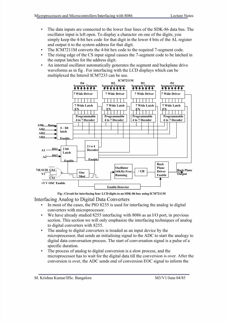
8/14/2019 microprocessor and microcontroller module 3
http://slidepdf.com/reader/full/microprocessor-and-microcontroller-module-3 85/91
Microprocessors and Microcontrollers/Interfacing with 8086 Lecture Notes
• The data inputs are connected to the lower four lines of the SDK-86 data bus. The
oscillator input is left open. To display a character on one of the digits, you
simply keep the 4-bit hex code for that digit in the lower 4 bits of the AL register and output it to the system address for that digit.
• The ICM7211M converts the 4-bit hex code to the required 7-segment code.
•
The rising edge of the CS input signal causes the 7-segment code to be latched inthe output latches for the address digit.
• An internal oscillator automatically generates the segment and backplane drive
waveforms as in fig . For interfacing with the LCD displays which can bemultiplexed the Intersil ICM7233 can be use.
Interfacing Analog to Digital Data Converters• In most of the cases, the PIO 8255 is used for interfacing the analog to digital
converters with microprocessor.
• We have already studied 8255 interfacing with 8086 as an I/O port, in previoussection. This section we will only emphasize the interfacing techniques of analog
to digital converters with 8255.• The analog to digital converters is treaded as an input device by the
microprocessor, that sends an initialising signal to the ADC to start the analogy todigital data conversation process. The start of conversation signal is a pulse of a
specific duration.
• The process of analog to digital conversion is a slow process, and themicroprocessor has to wait for the digital data till the conversion is over. After the
conversion is over, the ADC sends end of conversion EOC signal to inform the
Programmable
4 to 7 Decoder
7 Wide Latch
EN
7 Wide Driver
Programmable
4 to 7 Decoder
7 Wide Latch
EN
7 Wide Driver
Programmable
4 to 7 Decoder
7 Wide Latch
EN
7 Wide Driver
Programmable
4 to 7 Decoder
7 Wide Latch
EN
7 Wide Driver
Enable Detector
Back
PlaneDriver
Enable
Back PlaneOutput
Oscillator
16KHz Free
Running
/ 128One
Shot
2 t o 4
Decoder
Enable
+5 V OSC Enable
74LS138Y2
CS2
CS1
A1
A2
2 bit
Latch
Enable
4 – bit
latch
Enable
DataAD0
AD1
AD2
AD3
DS1
DS2
Segment OutputsD4
Segment Outputs Segment OutputsD3
ICM7211M
Segment OutputsD2 D1
Fig : Circuit for interfacing four LCD digits to an SDK-86 bus using ICM7211M
M. Krishna Kumar/IISc. Bangalore M3/V1/June 04/85

8/14/2019 microprocessor and microcontroller module 3
http://slidepdf.com/reader/full/microprocessor-and-microcontroller-module-3 86/91
Microprocessors and Microcontrollers/Interfacing with 8086 Lecture Notes
microprocessor that the conversion is over and the result is ready at the output
buffer of the ADC. These tasks of issuing an SOC pulse to ADC, reading EOC
signal from the ADC and reading the digital output of the ADC are carried out bythe CPU using 8255 I/O ports.
• The time taken by the ADC from the active edge of SOC pulse till the active edge
of EOC signal is called as the conversion delay of the ADC.• It may range any where from a few microseconds in case of fast ADC to even a
few hundred milliseconds in case of slow ADCs.
• The available ADC in the market use different conversion techniques for conversion of analog signal to digitals. Successive approximation techniques and
dual slope integration techniques are the most popular techniques used in the
integrated ADC chip.• General algorithm for ADC interfacing contains the following steps:
1. Ensure the stability of analog input, applied to the ADC.
2. Issue start of conversion pulse to ADC
3. Read end of conversion signal to mark the end of conversion processes.
4.
Read digital data output of the ADC as equivalent digital output.5. Analog input voltage must be constant at the input of the ADC right from the start
of conversion till the end of the conversion to get correct results. This may beensured by a sample and hold circuit which samples the analog signal and holds it
constant for a specific time duration. The microprocessor may issue a hold signal
to the sample and hold circuit.6. If the applied input changes before the complete conversion process is over, the
digital equivalent of the analog input calculated by the ADC may not be correct.
ADC 0808/0809 :
• The analog to digital converter chips 0808 and 0809 are 8-bit CMOS, successiveapproximation converters. This technique is one of the fast techniques for analogto digital conversion. The conversion delay is 100µs at a clock frequency of 640
KHz, which is quite low as compared to other converters. These converters do not
need any external zero or full scale adjustments as they are already taken care of
by internal circuits. These converters internally have a 3:8 analog multiplexer sothat at a time eight different analog conversion by using address lines -
ADD A, ADD B, ADD C. Using these address inputs, multichannel data acquisition
system can be designed using a single ADC. The CPU may drive these lines using output port lines in case of multichannel applications. In case of single input applications, these
may be hardwired to select the proper input.
• There are unipolar analog to digital converters, i.e. they are able to convert only positive analog input voltage to their digital equivalent. These chips do no contain
any internal sample and hold circuit.
M. Krishna Kumar/IISc. Bangalore M3/V1/June 04/86

8/14/2019 microprocessor and microcontroller module 3
http://slidepdf.com/reader/full/microprocessor-and-microcontroller-module-3 87/91
Microprocessors and Microcontrollers/Interfacing with 8086 Lecture Notes
Address linesAnalog /P
selecte C B A
• If one needs a sample and hold circuit for the conversion of fast signal intoequivalent digital quantities, it has to be externally connected at each of the
analog inputs.
• Vcc Supply pins +5V
• GND GND• Vref + Reference voltage positive +5 Volts maximum.• Vref + Reference voltage positive +5 Volts maximum.
• Vref _ Reference voltage negative 0Volts minimum.• Vref _ Reference voltage negative 0Volts minimum.
• I/P0 –I/P7 Analog inputs• I/P0 –I/P7 Analog inputs• ADD A,B,C Address lines for selecting analog inputs.• ADD A,B,C Address lines for selecting analog inputs.
• O7 – O0 Digital 8-bit output with O7 MSB and O0 LSB• O7 – O0 Digital 8-bit output with O7 MSB and O0 LSB
• SOC Start of conversion signal pin• SOC Start of conversion signal pin
• EOC End of conversion signal pin• EOC End of conversion signal pin• OE Output latch enable pin, if high enables output• OE Output latch enable pin, if high enables output
• CLK Clock input for ADC• CLK Clock input for ADC
I / P 0 0 00
I / P 0 0 11
I / P 0 1 02
0 1 1I / P 3
1 0 0I / P 4
1 0 1I / P 5
1 1 0I / P 6
1 1 1I / P 7
M. Krishna Kumar/IISc. Bangalore M3/V1/June 04/87
8/14/2019 microprocessor and microcontroller module 3
http://slidepdf.com/reader/full/microprocessor-and-microcontroller-module-3 88/91
Microprocessors and Microcontrollers/Interfacing with 8086 Lecture Notes
CLOCOC K SI / P 0
EOCI / P 1
Control and
Timing unit
• Example: Interfacing ADC 0808 with 8086 using 8255 ports. Use port A of 8255for transferring digital data output of ADC to the CPU and port C for control
O/PLa tch
O/PEnable
8- bitO/P
and .A.R.
256 R R egister
ladder andSwitch tree
V ref + V ref _
8 ChannelAnalog
Mul tiplexer
ABC
I / P 2
I / P 3
I / P 4
I / P 5
I / P 6
I / P7
Address
Block Diagram of ADC 0808 / 0809
C L OC K
ST AR T
AL E
EO C
OE
O / P
Timing Diagram of ADC 0808
M. Krishna Kumar/IISc. Bangalore M3/V1/June 04/88
8/14/2019 microprocessor and microcontroller module 3
http://slidepdf.com/reader/full/microprocessor-and-microcontroller-module-3 89/91
Microprocessors and Microcontrollers/Interfacing with 8086 Lecture Notes
signals. Assume that an analog input is present at I/P2 of the ADC and a clock
input of suitable frequency is available for ADC.
• Solution: The analog input I/P2 is used and therefore address pins A,B,C should be 0,1,0 respectively to select I/P2. The OE and ALE pins are already kept at +5V
to select the ADC and enable the outputs. Port C upper acts as the input port to
receive the EOC signal while port C lower acts as the output port to send SOC tothe ADC.
• Port A acts as a 8-bit input data port to receive the digital data output from the
ADC. The 8255 control word is written as follows:D7 D6 D5 D4 D3 D2 D1 D0
1 0 0 1 1 0 0 0
• The required ALP is as follows:MOV AL, 98h ;initialise 8255 as
OUT CWR, AL ;discussed above.
MOV AL, 02h ;Select I/P2 as analog
OUT Port B, AL ;input.
MOV AL, 00h ;Give start of conversionOUT Port C, AL ; pulse to the ADC
MOV AL, 01hOUT Port C, AL
MOV AL, 00h
OUT Port C, ALWAIT: IN AL, Port C ;Check for EOC by
RCR ; reading port C upper and
JNC WAIT ;rotating through carry.
IN AL, Port A ;If EOC, read digital equivalent in ALHLT ;Stop.
M. Krishna Kumar/IISc. Bangalore M3/V1/June 04/89

8/14/2019 microprocessor and microcontroller module 3
http://slidepdf.com/reader/full/microprocessor-and-microcontroller-module-3 90/91
Microprocessors and Microcontrollers/Interfacing with 8086 Lecture Notes
Vref +
Interfacing Digital To Analog Converters INTERFACING DIGITAL TO ANALOG CONVERTERS: The digital to analog
converters convert binary number into their equivalent voltages. The DAC find
applications in areas like digitally controlled gains, motors speed controls, programmablegain amplifiers etc.
AD 7523 8-bit Multiplying DAC : This is a 16 pin DIP, multiplying digital to
analog converter, containing R-2R ladder for D-A conversion along with single poledouble thrown NMOS switches to connect the digital inputs to the ladder.
• The pin diagram of AD7523 is shown in fig the supply range is from +5V to
+15V, while Vref may be any where between -10V to +10V. The maximumanalog output voltage will be any where between -10V to +10V, when all the
digital inputs are at logic high state.
• Usually a zener is connected between OUT1 and OUT2 to save the DAC fromnegative transients. An operational amplifier is used as a current to voltage
converter at the output of AD to convert the current out put of AD to a
proportional output voltage.
• It also offers additional drive capability to the DAC output. An external feedback resistor acts to control the gain. One may not connect any external feedback
resistor, if no gain control is required.• EXAMPLE: Interfacing DAC AD7523 with an 8086 CPU running at 8MHZ and
write an assembly language program to generate a sawtooth waveform of period
1ms with Vmax 5V.
• Solution: Fig shows the interfacing circuit of AD 74523 with 8086 using 8255. program gives an ALP to generate a sawtooth waveform using circuit.
Interfacing 0808 with 8086
CS
D0 – D7
Vref +
+ 5 V
Clock up+ 5 V Vcc
PA7 – PA0 O7 – O0
ADC
0808
AnalogI/P
Voltage
EOCPC7A2
PC0 SOCA1
OE GND
8255Reset
CA
ALE+5V B
IORD
PB1
PB0
IOWR PB2
M. Krishna Kumar/IISc. Bangalore M3/V1/June 04/90

8/14/2019 microprocessor and microcontroller module 3
http://slidepdf.com/reader/full/microprocessor-and-microcontroller-module-3 91/91