Embed Size (px)
Citation preview
EC0122 ELECTRIC CIRCUITS LABORATORY
Laboratory Manual
DEPARTMENT OF TELECOMMUNICATION ENGINEERING
SRM UNIVERSITY S.R.M. NAGAR, KATTANKULATHUR – 603 203.
FOR PRIVATE CIRCULATION ONLY
ALL RIGHTS RESERVED
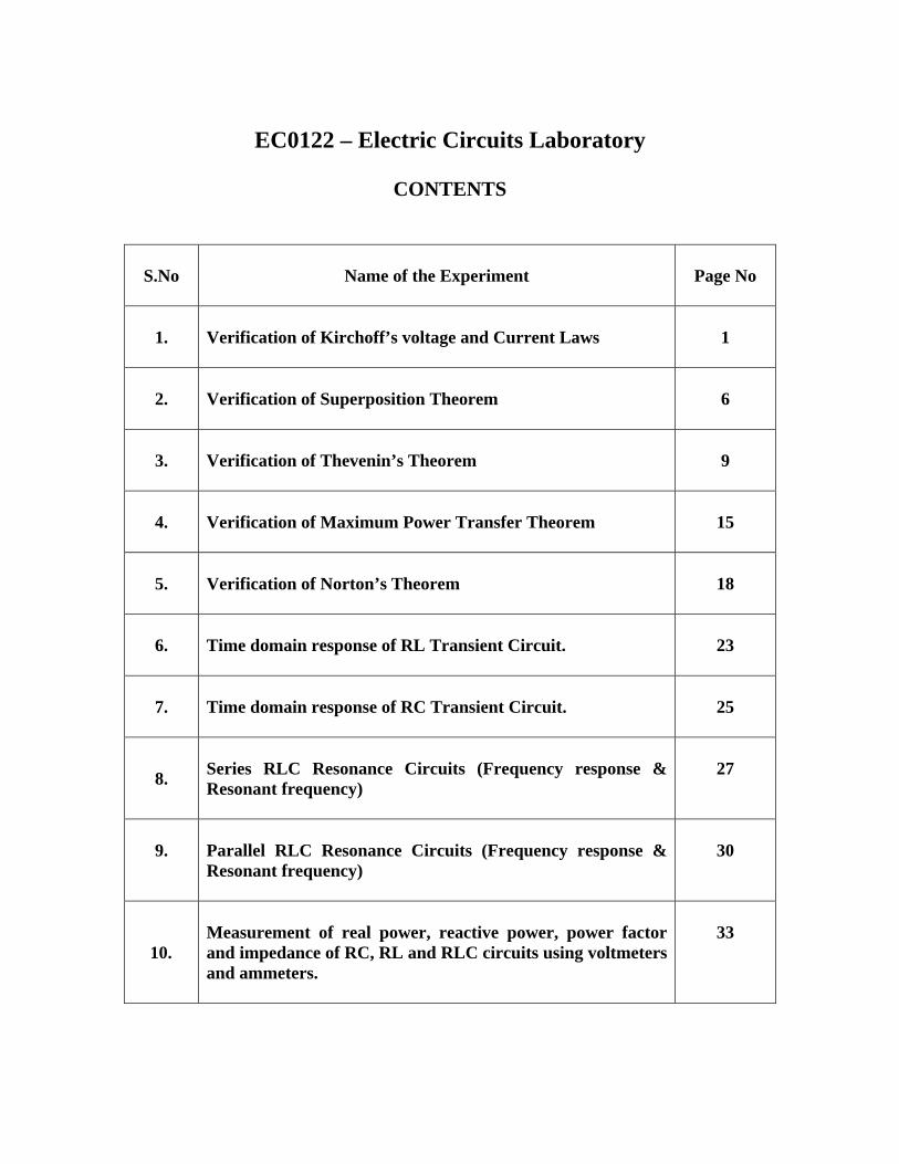
EC0122 – Electric Circuits Laboratory
CONTENTS
S.No
Name of the Experiment Page No
1.
Verification of Kirchoff’s voltage and Current Laws
1
2.
Verification of Superposition Theorem
6
3.
Verification of Thevenin’s Theorem
9
4.
Verification of Maximum Power Transfer Theorem
15
5.
Verification of Norton’s Theorem
18
6.
Time domain response of RL Transient Circuit.
23
7.
Time domain response of RC Transient Circuit.
25
8.
Series RLC Resonance Circuits (Frequency response & Resonant frequency)
27
9.
Parallel RLC Resonance Circuits (Frequency response & Resonant frequency)
30
10.
Measurement of real power, reactive power, power factor and impedance of RC, RL and RLC circuits using voltmeters and ammeters.
33
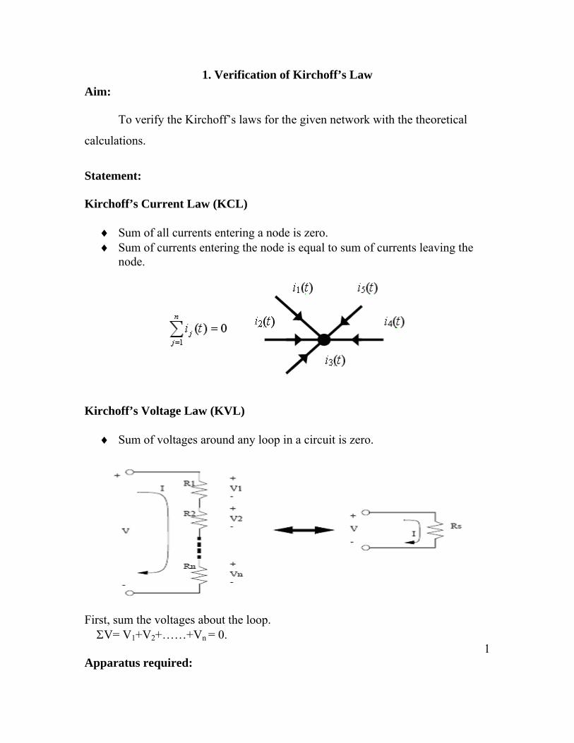
1. Verification of Kirchoff’s Law Aim: To verify the Kirchoff’s laws for the given network with the theoretical
calculations.
Statement: Kirchoff’s Current Law (KCL)
♦ Sum of all currents entering a node is zero. ♦ Sum of currents entering the node is equal to sum of currents leaving the
node.
Kirchoff’s Voltage Law (KVL) ♦ Sum of voltages around any loop in a circuit is zero.
First, sum the voltages about the loop. ΣV= V1+V2+……+Vn = 0.
1 Apparatus required:
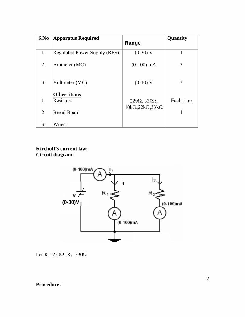
S.No Apparatus Required
Range Quantity
1.
2.
3.
1.
2.
3.
Regulated Power Supply (RPS) Ammeter (MC) Voltmeter (MC) Other items Resistors Bread Board Wires
(0-30) V
(0-100) mA
(0-10) V
220Ω, 330Ω, 10kΩ,22kΩ,33kΩ
1 3 3
Each 1 no 1
Kirchoff’s current law: Circuit diagram:
Let R1=220Ω; R2=330Ω
2 Procedure:
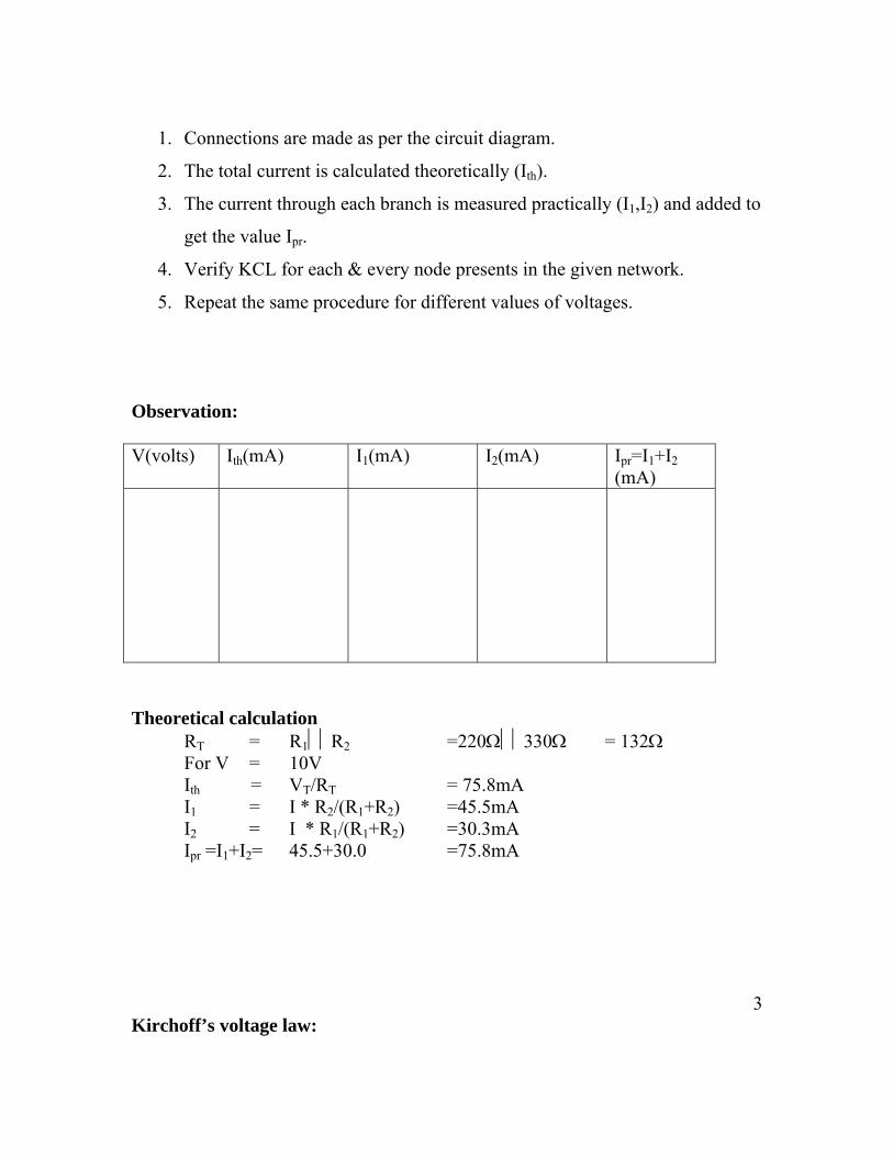
1. Connections are made as per the circuit diagram.
2. The total current is calculated theoretically (Ith).
3. The current through each branch is measured practically (I1,I2) and added to
get the value Ipr.
4. Verify KCL for each & every node presents in the given network.
5. Repeat the same procedure for different values of voltages. Observation: V(volts) Ith(mA) I1(mA) I2(mA) Ipr=I1+I2
(mA)
Theoretical calculation RT = R1R2 =220Ω330Ω = 132Ω For V = 10V Ith = VT/RT = 75.8mA I1 = I * R2/(R1+R2) =45.5mA I2 = I * R1/(R1+R2) =30.3mA Ipr =I1+I2= 45.5+30.0 =75.8mA
3 Kirchoff’s voltage law:
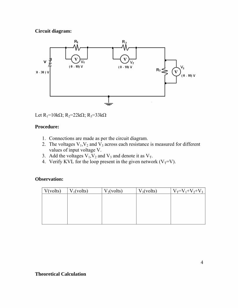
Circuit diagram:
Let R1=10kΩ; R2=22kΩ; R3=33kΩ Procedure:
1. Connections are made as per the circuit diagram. 2. The voltages V1,V2 and V3 across each resistance is measured for different
values of input voltage V. 3. Add the voltages V1,V2 and V3 and denote it as VT. 4. Verify KVL for the loop present in the given network (VT=V).
Observation:
V(volts) V1(volts) V2(volts) V3(volts) VT=V1+V2+V3
4 Theoretical Calculation
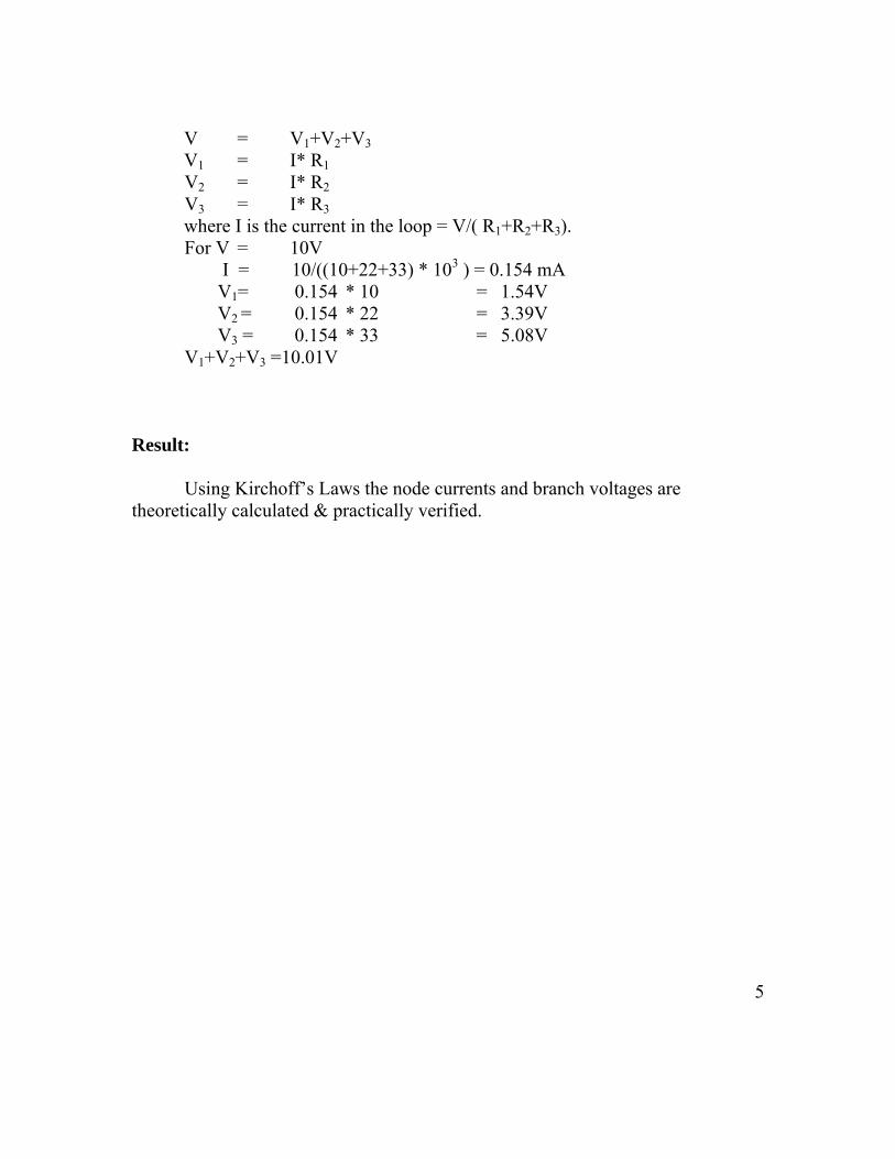
V = V1+V2+V3 V1 = I* R1 V2 = I* R2 V3 = I* R3 where I is the current in the loop = V/( R1+R2+R3).
For V = 10V I = 10/((10+22+33) * 103 ) = 0.154 mA
V1= 0.154 * 10 = 1.54V V2 = 0.154 * 22 = 3.39V V3 = 0.154 * 33 = 5.08V V1+V2+V3 =10.01V Result: Using Kirchoff’s Laws the node currents and branch voltages are theoretically calculated & practically verified.
5
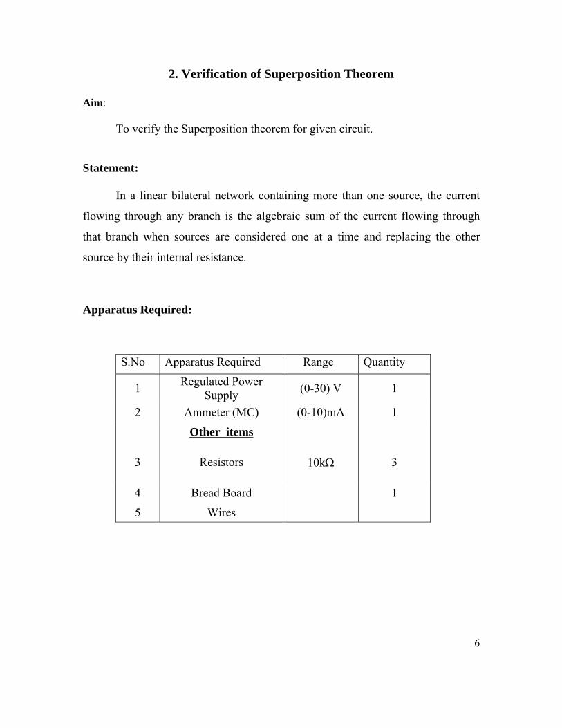
2. Verification of Superposition Theorem Aim:
To verify the Superposition theorem for given circuit.
Statement: In a linear bilateral network containing more than one source, the current
flowing through any branch is the algebraic sum of the current flowing through
that branch when sources are considered one at a time and replacing the other
source by their internal resistance.
Apparatus Required:
S.No Apparatus Required Range Quantity
1 Regulated Power Supply (0-30) V 1
2 Ammeter (MC) (0-10)mA 1
Other items
3 Resistors 10kΩ 3
4 Bread Board 1
5 Wires
6
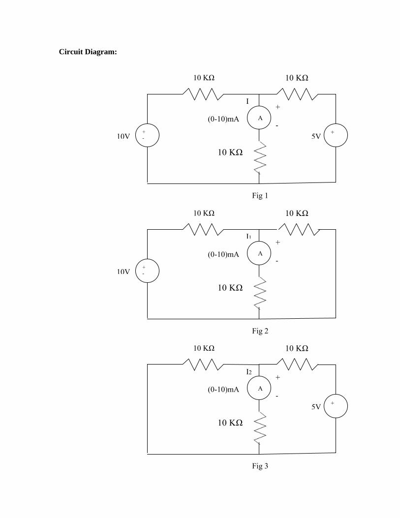
Circuit Diagram:
10 KΩ
+ - 10V
A
10 KΩ
10 KΩ
(0-10)mA +
- 5V
I
Fig 1
+
+ -
10 KΩ
10V
A
10 KΩ
10 KΩ
(0-10)mA
+ -
I1
Fig 2
10 KΩ
A
10 KΩ
10 KΩ
I2 +
(0-10)mA -
5V +
Fig 3
Procedure:
1. Connect the circuit as per the circuit diagram (Fig 1).
2. Switch on the DC power supplies (10V and 5V) and note down the
corresponding ammeter reading (Ipr).
3. Replace the second power supply (5V) by short circuit.
4. Switch on the power supply (10V) and note down the corresponding
ammeter reading (I1).
5. Connect the second power supply (5V) and replace the first power supply
by short circuit.
6. Switch on the power supply (5V) and note down the corresponding
ammeter reading (I2).
7. Verify the following condition
Ipr = I1 +I2
8. Calculate I1 , I2 theoretically using mesh equations then find Ith= I1+I2 and
compare with the Practical value Ipr.
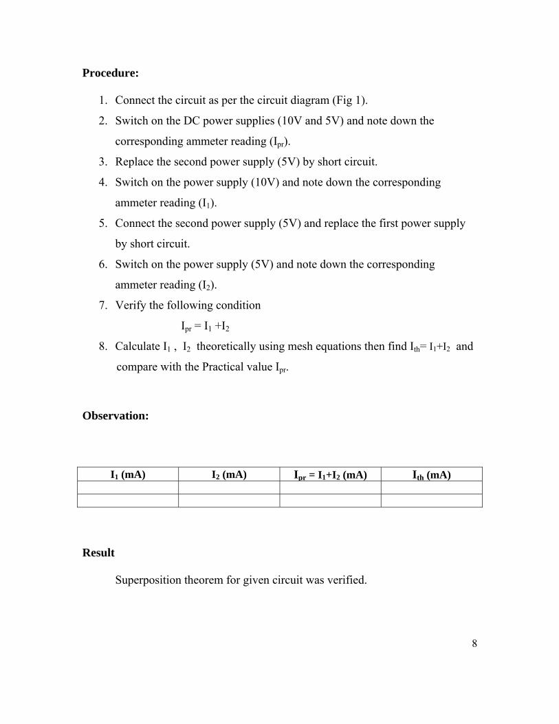
Observation:
I1 (mA) I2 (mA) Ipr = I1+I2 (mA) Ith (mA) Result Superposition theorem for given circuit was verified.
8
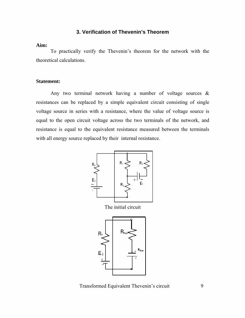
3. Verification of Thevenin’s Theorem Aim: To practically verify the Thevenin’s theorem for the network with the
theoretical calculations.
Statement: Any two terminal network having a number of voltage sources &
resistances can be replaced by a simple equivalent circuit consisting of single
voltage source in series with a resistance, where the value of voltage source is
equal to the open circuit voltage across the two terminals of the network, and
resistance is equal to the equivalent resistance measured between the terminals
with all energy source replaced by their internal resistance.
The initial circuit
Transformed Equivalent Thevenin’s circuit 9
Apparatus Required:
S.No Apparatus Required Range Quantity
1 2 3 4 5
Regulated Power Supply Voltmeter (MC) Other items Resistors Bread Board Wires
(0-30) V
(0-10) V
220Ω 330Ω, 1kΩ
1 1
Each 1 no 1
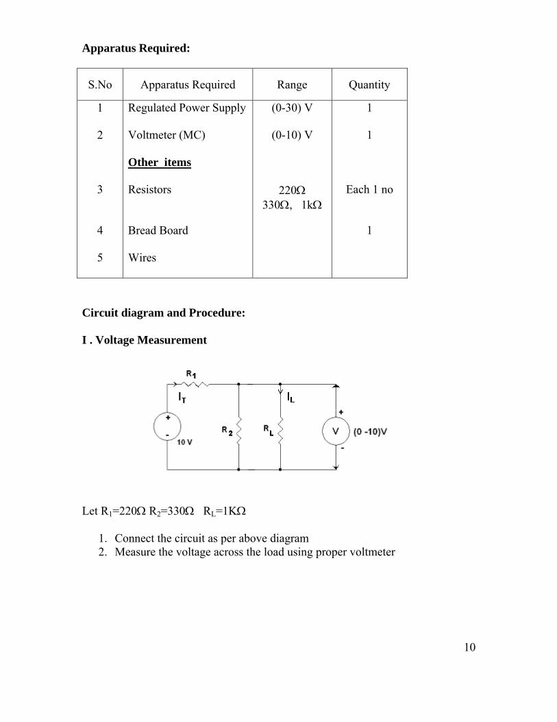
Circuit diagram and Procedure: I . Voltage Measurement
Let R1=220Ω R2=330Ω RL=1KΩ
1. Connect the circuit as per above diagram 2. Measure the voltage across the load using proper voltmeter
10
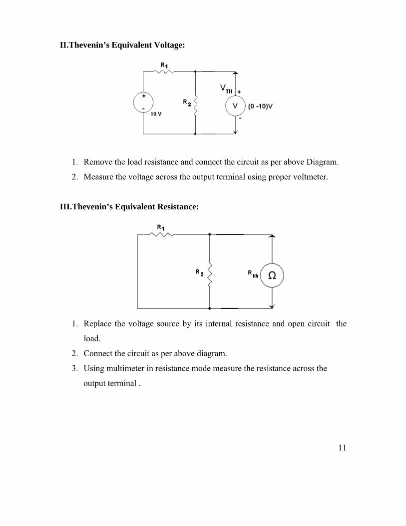
II.Thevenin’s Equivalent Voltage:
1. Remove the load resistance and connect the circuit as per above Diagram.
2. Measure the voltage across the output terminal using proper voltmeter.
III.Thevenin’s Equivalent Resistance:
1. Replace the voltage source by its internal resistance and open circuit the
load.
2. Connect the circuit as per above diagram.
3. Using multimeter in resistance mode measure the resistance across the
output terminal .
11
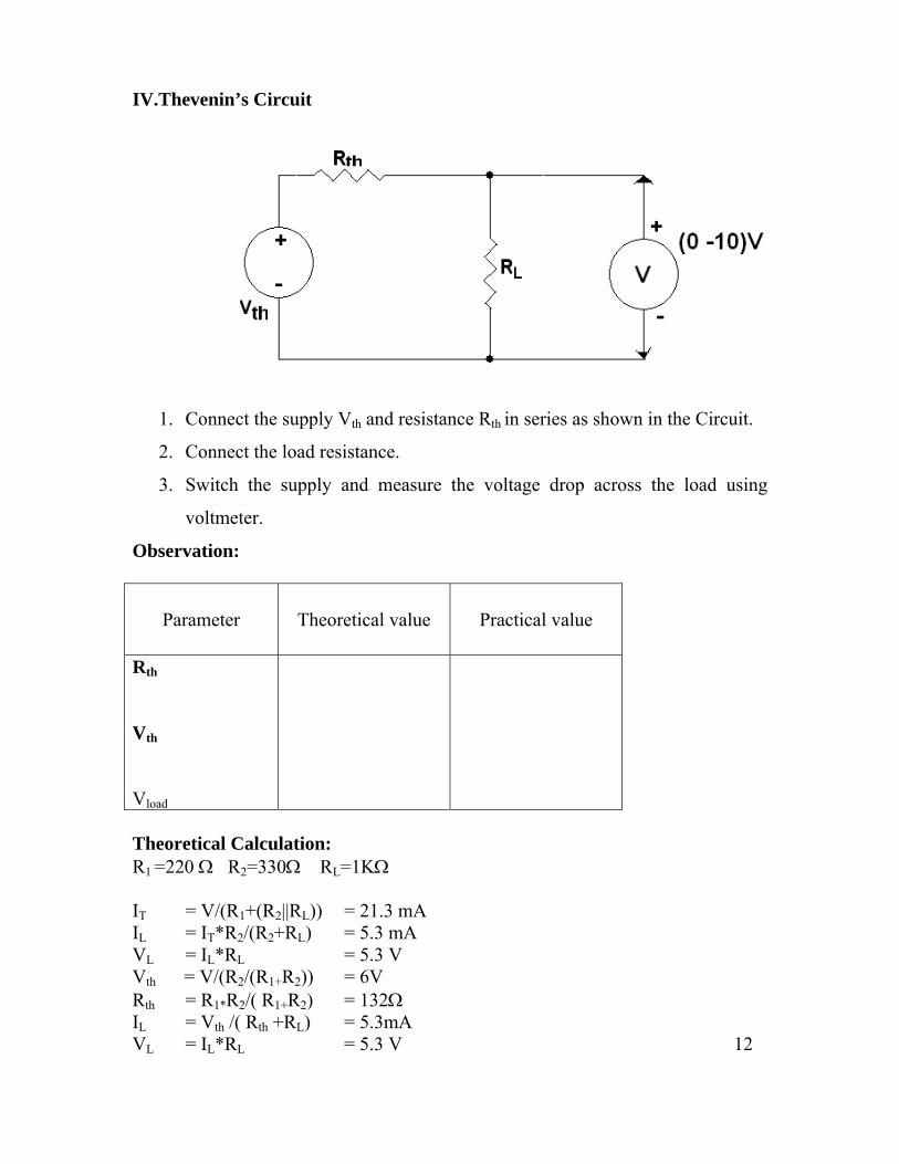
IV.Thevenin’s Circuit
1. Connect the supply Vth and resistance Rth in series as shown in the Circuit.
2. Connect the load resistance.
3. Switch the supply and measure the voltage drop across the load using
voltmeter.
Observation:
Parameter Theoretical value Practical value
Rth Vth Vload
Theoretical Calculation: R1 =220 Ω R2=330Ω RL=1KΩ IT = V/(R1+(R2||RL)) = 21.3 mA IL = IT*R2/(R2+RL) = 5.3 mA VL = IL*RL = 5.3 V Vth = V/(R2/(R1+R2)) = 6V Rth = R1*R2/( R1+R2) = 132Ω IL = Vth /( Rth +RL) = 5.3mA VL = IL*RL = 5.3 V 12
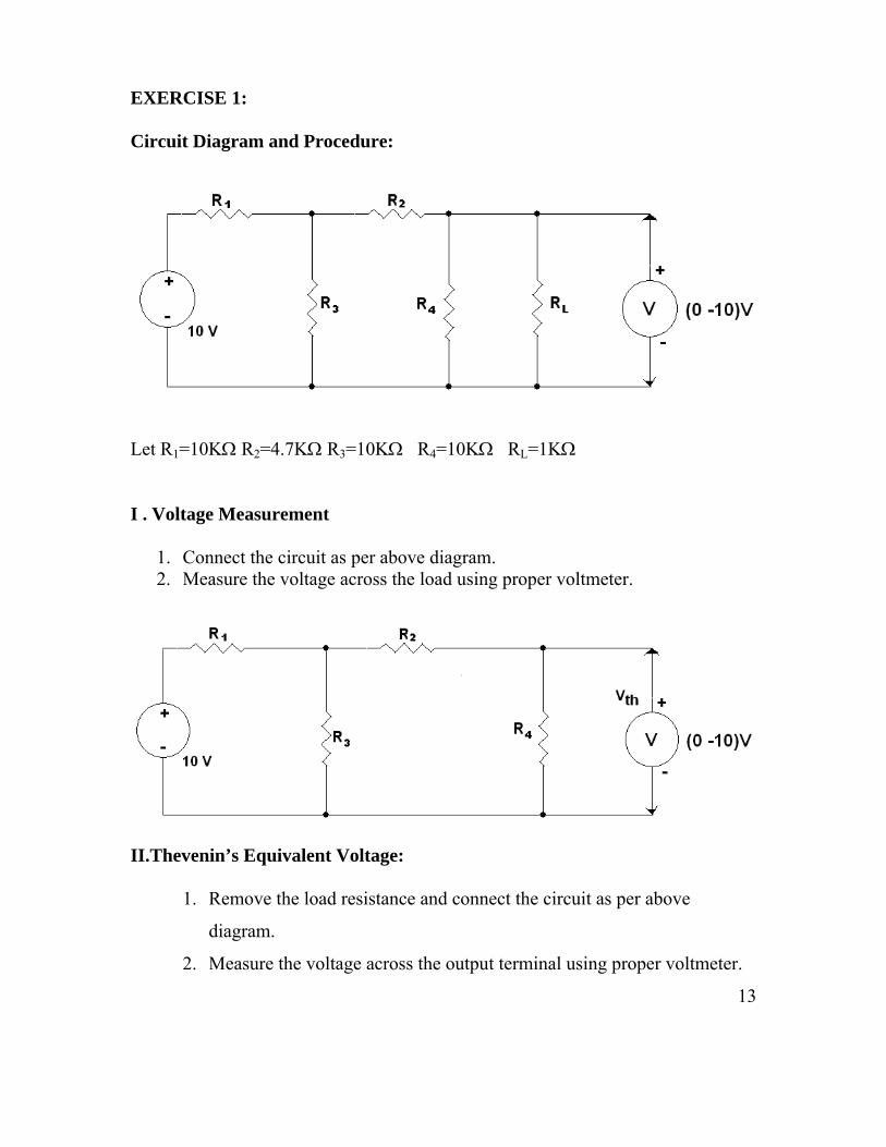
EXERCISE 1: Circuit Diagram and Procedure:
Let R1=10KΩ R2=4.7KΩ R3=10KΩ R4=10KΩ RL=1KΩ I . Voltage Measurement
1. Connect the circuit as per above diagram. 2. Measure the voltage across the load using proper voltmeter.
II.Thevenin’s Equivalent Voltage:
1. Remove the load resistance and connect the circuit as per above
diagram.
2. Measure the voltage across the output terminal using proper voltmeter.
13
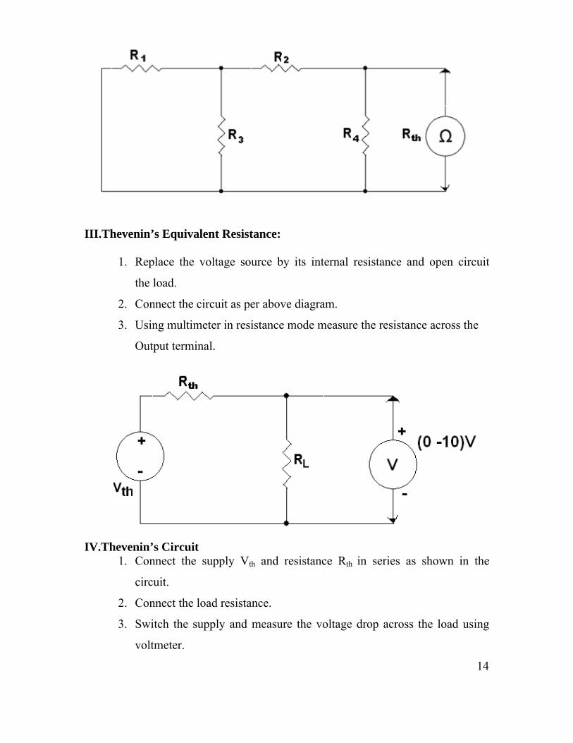
III.Thevenin’s Equivalent Resistance:
1. Replace the voltage source by its internal resistance and open circuit
the load.
2. Connect the circuit as per above diagram.
3. Using multimeter in resistance mode measure the resistance across the
Output terminal.
IV.Thevenin’s Circuit
1. Connect the supply Vth and resistance Rth in series as shown in the
circuit.
2. Connect the load resistance.
3. Switch the supply and measure the voltage drop across the load using
voltmeter.
14
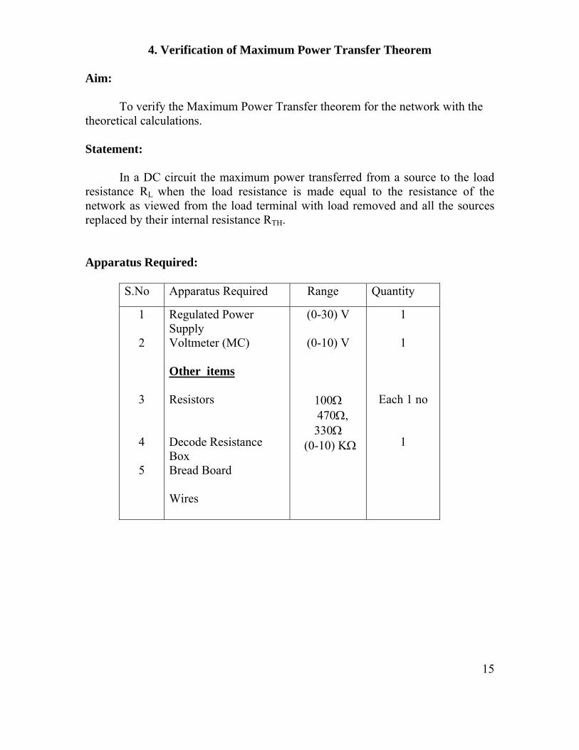
4. Verification of Maximum Power Transfer Theorem Aim: To verify the Maximum Power Transfer theorem for the network with the theoretical calculations. Statement: In a DC circuit the maximum power transferred from a source to the load resistance RL when the load resistance is made equal to the resistance of the network as viewed from the load terminal with load removed and all the sources replaced by their internal resistance RTH. Apparatus Required:
S.No Apparatus Required Range Quantity
1 2 3 4 5
Regulated Power Supply Voltmeter (MC) Other items Resistors Decode Resistance Box Bread Board Wires
(0-30) V
(0-10) V
100Ω 470Ω,
330Ω (0-10) KΩ
1 1
Each 1 no 1
15
Circuit Diagram:
Let R1= 100Ω R2= 330Ω R3= 470Ω Procedure
1. Remove the portion of the network through which maximum power has to be transferred.
2. Name those terminals as A&B. 3. Calculate Rth by substituting all sources with their internal resistances
looking back at the network. 4. Give the connection as per the circuit diagram. 5. By varying the DRB (RL), for various values of RL, measure the current
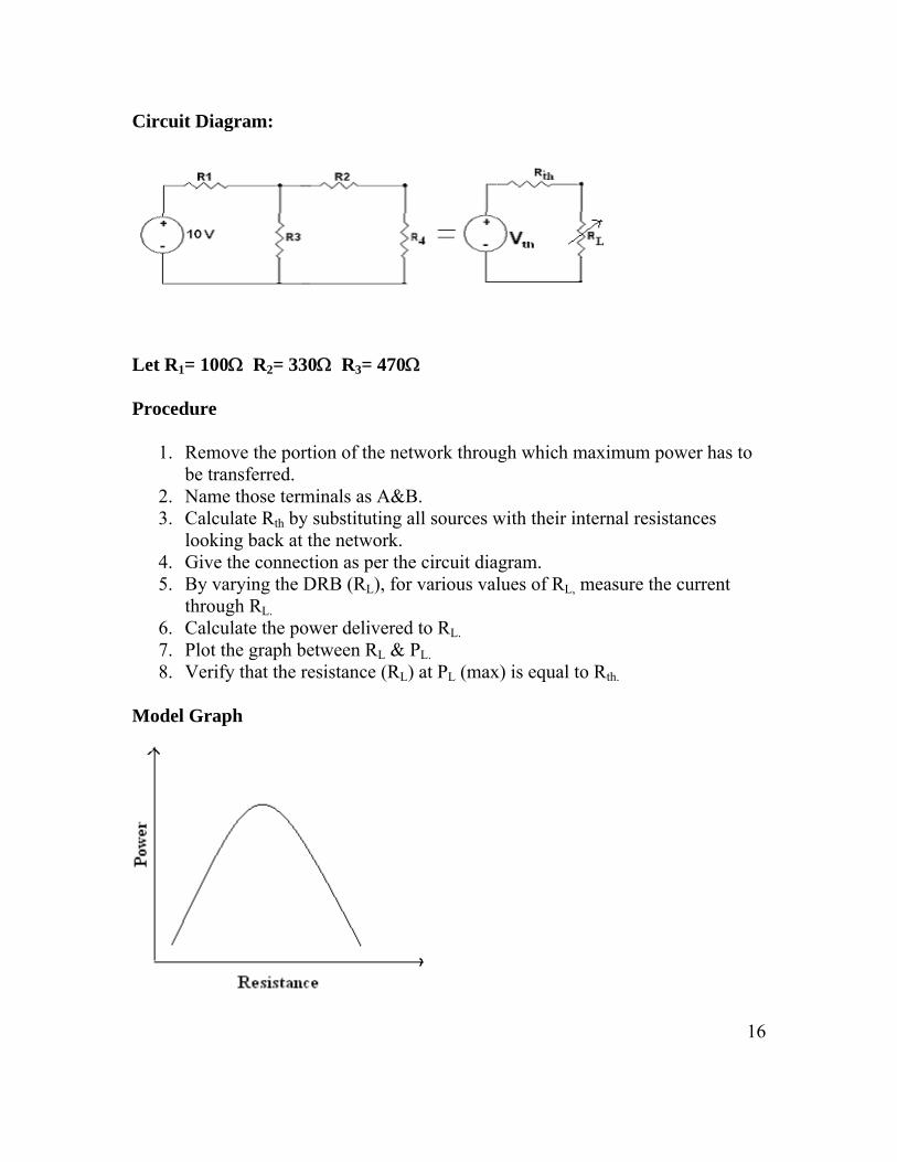
through RL. 6. Calculate the power delivered to RL. 7. Plot the graph between RL & PL. 8. Verify that the resistance (RL) at PL (max) is equal to Rth.
Model Graph
16
Theoretical Verification: Rth = (100Ω 470Ω) + 330Ω = 82.46 +330 = 412.45Ω Equivalent voltage = (10x470)/570 = 8.2456 V Current through load resistance = 8.24256/ (412+412) = 10mA Power dissipated across the resistance=I2 x RL = 100 * 10-6 * 412.45 = 41.4475mwatts. Result: Using Maximum Power Transfer theorem, theoretically calculated values of RL & PL are verified with the practically measured values.
17
5. Verification of Norton’s Theorem Aim: To verify the Norton’s theorem for the network with the theoretical calculations. Statement:
Any two terminal linear networks with current source, voltage source and resistances can be replaced by an equivalent circuit consisting of a current source in parallel with a resistance. The value of current source is the short circuit between the two terminal of the network and resistance is equal to the equivalent resistance measured between the terminals with all energy source replaced by their internal resistance. Apparatus Required:
S.No Apparatus Required Range Quantity
1 Regulated Power Supply (0-30) V 1
2 Voltmeter (MC) (0-10) V 1
Other items
3 Resistors 220Ω 330Ω, 1kΩ Each 1 no
4 Bread Board 1
5 Wires 18
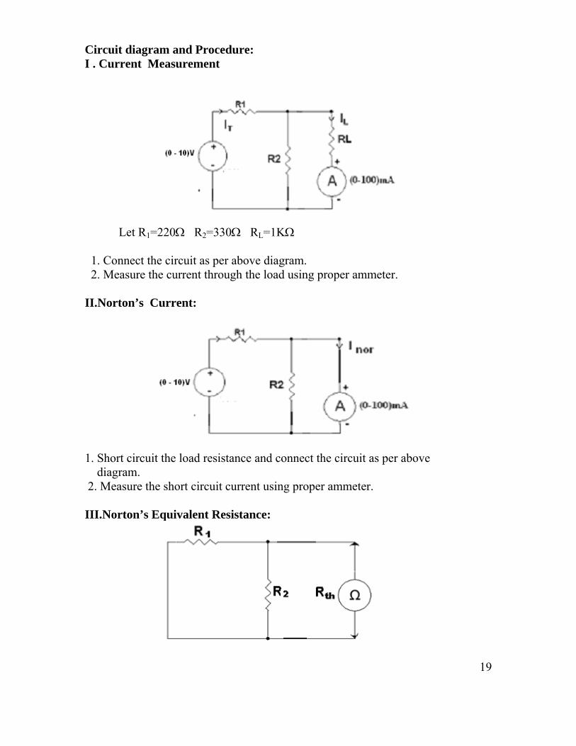
Circuit diagram and Procedure: I . Current Measurement
Let R1=220Ω R2=330Ω RL=1KΩ
1. Connect the circuit as per above diagram. 2. Measure the current through the load using proper ammeter. II.Norton’s Current:
1. Short circuit the load resistance and connect the circuit as per above diagram. 2. Measure the short circuit current using proper ammeter. III.Norton’s Equivalent Resistance:
19
1. Replace the source by its internal resistance and open circuit the load. 2. Connect the circuit as per above diagram. 3. Using multimeter in resistance mode measure the resistance across the
output terminal.
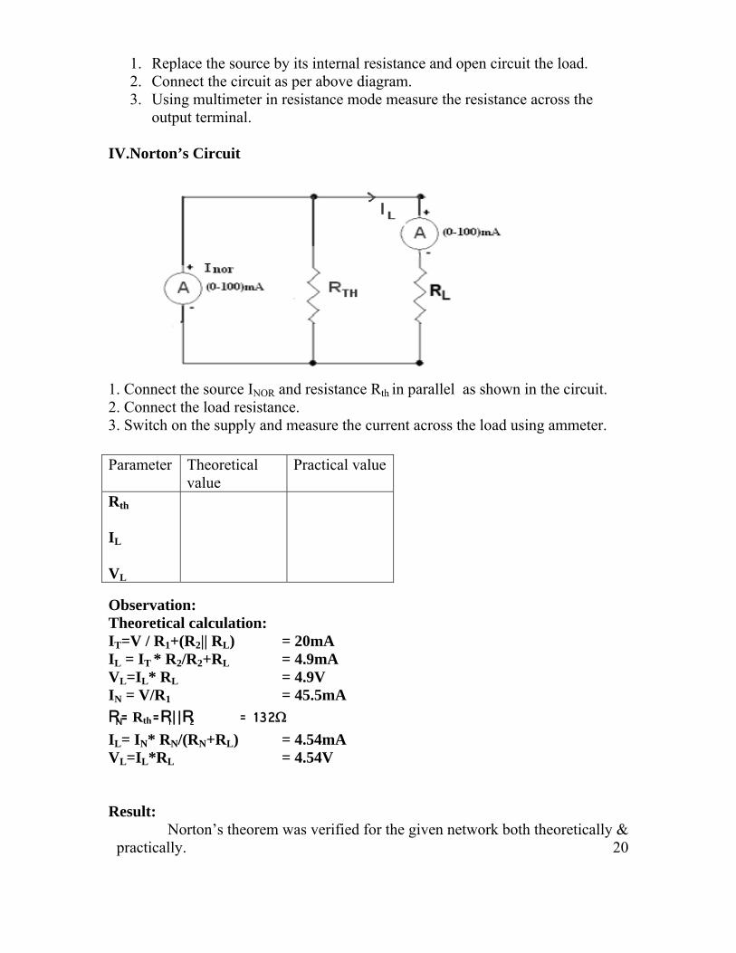
IV.Norton’s Circuit
1. Connect the source INOR and resistance Rth in parallel as shown in the circuit. 2. Connect the load resistance. 3. Switch on the supply and measure the current across the load using ammeter.
Parameter Theoretical value
Practical value
Rth IL
VL
Observation: Theoretical calculation: IT=V / R1+(R2|| RL) = 20mA IL = IT * R2/R2+RL = 4.9mA VL=IL* RL = 4.9V IN = V/R1 = 45.5mA RN= Rth R= 1 R|| 2 = 132Ω IL= IN* RN/(RN+RL) = 4.54mA VL=IL*RL = 4.54V Result:
Norton’s theorem was verified for the given network both theoretically & practically. 20
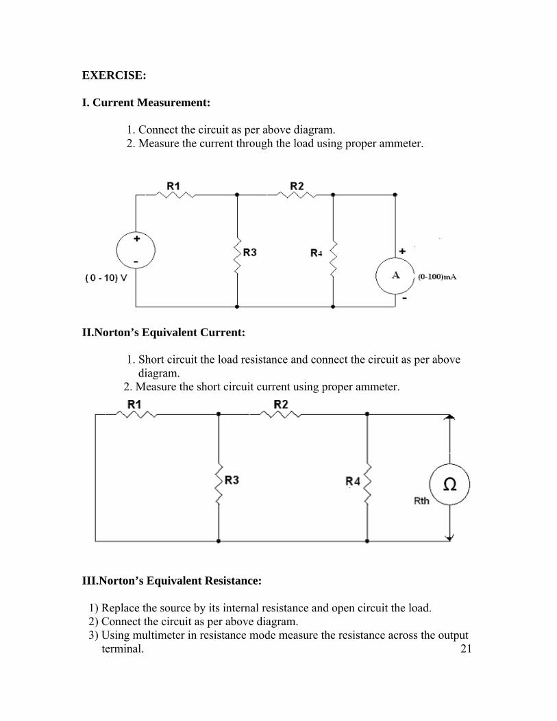
EXERCISE: I. Current Measurement: 1. Connect the circuit as per above diagram.
2. Measure the current through the load using proper ammeter.
II.Norton’s Equivalent Current: 1. Short circuit the load resistance and connect the circuit as per above diagram.
2. Measure the short circuit current using proper ammeter.
III.Norton’s Equivalent Resistance:
1) Replace the source by its internal resistance and open circuit the load. 2) Connect the circuit as per above diagram. 3) Using multimeter in resistance mode measure the resistance across the output
terminal. 21
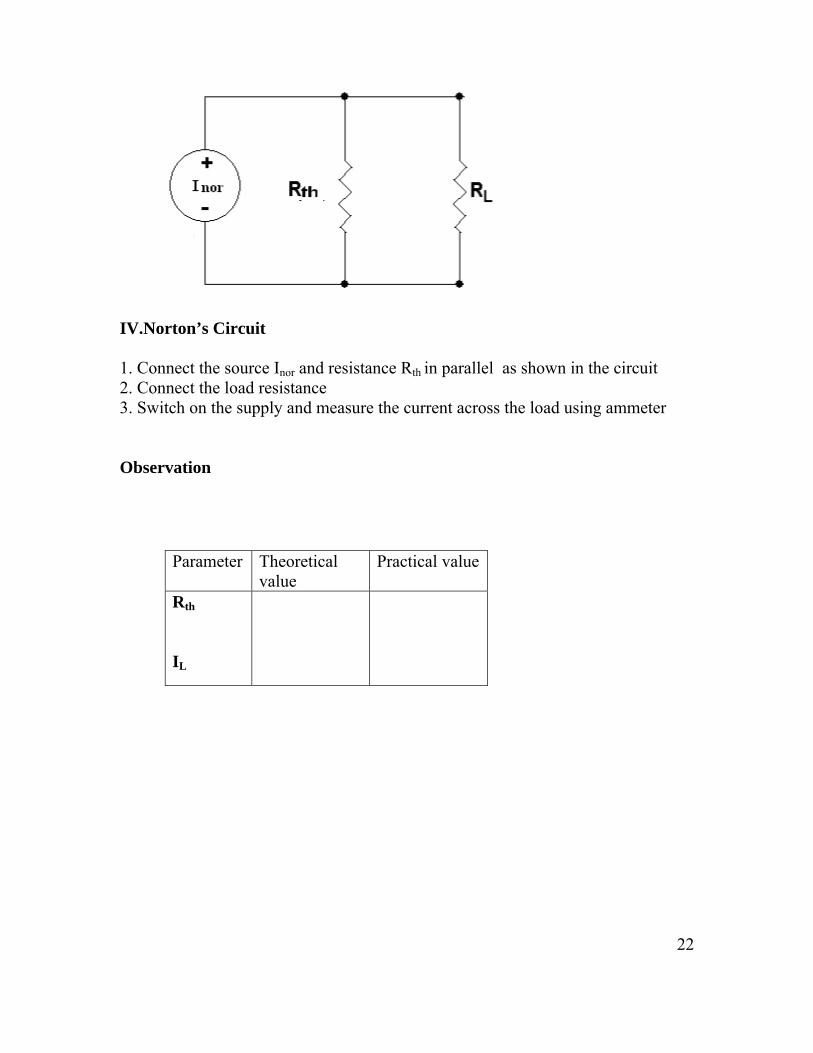
IV.Norton’s Circuit 1. Connect the source Inor and resistance Rth in parallel as shown in the circuit 2. Connect the load resistance 3. Switch on the supply and measure the current across the load using ammeter Observation
Parameter Theoretical value
Practical value
Rth IL
22
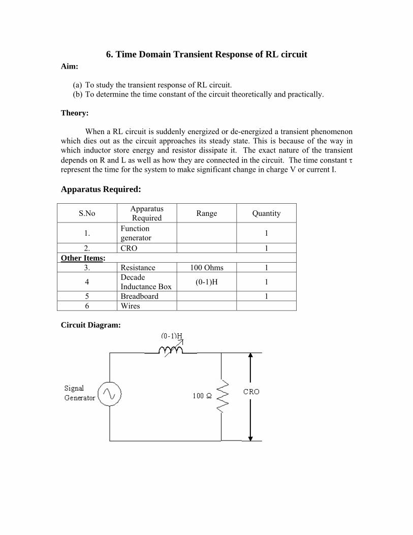
6. Time Domain Transient Response of RL circuit Aim:
(a) To study the transient response of RL circuit. (b) To determine the time constant of the circuit theoretically and practically.
Theory: When a RL circuit is suddenly energized or de-energized a transient phenomenon which dies out as the circuit approaches its steady state. This is because of the way in which inductor store energy and resistor dissipate it. The exact nature of the transient depends on R and L as well as how they are connected in the circuit. The time constant τ represent the time for the system to make significant change in charge V or current I.
Apparatus Required:
S.No Apparatus Required Range Quantity
1. Function generator 1
2. CRO 1 Other Items:
3. Resistance 100 Ohms 1
4 Decade Inductance Box (0-1)H 1
5 Breadboard 1 6 Wires
Circuit Diagram:
23
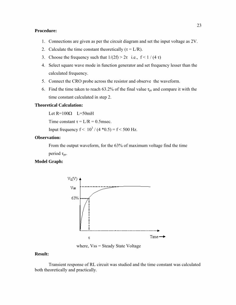
Procedure:
1. Connections are given as per the circuit diagram and set the input voltage as 2V.
2. Calculate the time constant theoretically (τ = L/R).
3. Choose the frequency such that 1/(2f) > 2τ i.e., f < 1 / (4 τ)
4. Select square wave mode in function generator and set frequency lesser than the
calculated frequency.
5. Connect the CRO probe across the resistor and observe the waveform.
6. Find the time taken to reach 63.2% of the final value τpr and compare it with the
time constant calculated in step 2.
Theoretical Calculation:
Let R=100Ω L=50mH
Time constant τ = L/R = 0.5msec.
Input frequency f < 103 / (4 *0.5) = f < 500 Hz.
Observation:
From the output waveform, for the 63% of maximum voltage find the time
period τpr.
Model Graph:
where, Vss = Steady State Voltage
Result: Transient response of RL circuit was studied and the time constant was calculated both theoretically and practically.
24
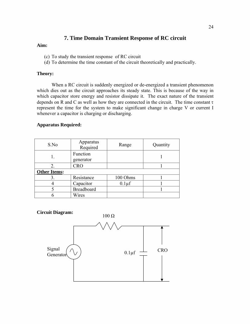
7. Time Domain Transient Response of RC circuit Aim:
(c) To study the transient response of RC circuit (d) To determine the time constant of the circuit theoretically and practically.
Theory: When a RC circuit is suddenly energized or de-energized a transient phenomenon which dies out as the circuit approaches its steady state. This is because of the way in which capacitor store energy and resistor dissipate it. The exact nature of the transient depends on R and C as well as how they are connected in the circuit. The time constant τ represent the time for the system to make significant change in charge V or current I whenever a capacitor is charging or discharging.
Apparatus Required:
S.No Apparatus Required Range Quantity
1. Function generator 1
2. CRO 1 Other Items:
3. Resistance 100 Ohms 1 4 Capacitor 0.1µf 1 5 Breadboard 1 6 Wires
100 Ω
0.1µf Signal Generator
CRO
Circuit Diagram:
25
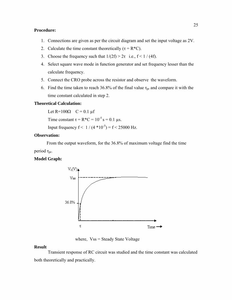
Procedure:
1. Connections are given as per the circuit diagram and set the input voltage as 2V.
2. Calculate the time constant theoretically (τ = R*C).
3. Choose the frequency such that 1/(2f) > 2τ i.e., f < 1 / (4f).
4. Select square wave mode in function generator and set frequency lesser than the
calculate frequency.
5. Connect the CRO probe across the resistor and observe the waveform.
6. Find the time taken to reach 36.8% of the final value τpr and compare it with the
time constant calculated in step 2.
Theoretical Calculation:
Let R=100Ω C = 0.1 µf
Time constant τ = R*C = 10-5 s = 0.1 µs.
Input frequency f < 1 / (4 *10-5) = f < 25000 Hz.
Observation:
From the output waveform, for the 36.8% of maximum voltage find the time
period τpr.
Model Graph:
where, Vss = Steady State Voltage Result Transient response of RC circuit was studied and the time constant was calculated
both theoretically and practically.
26
8. Parallel RLC Resonance Circuits
Aim:
To Study and plot the curve of Resonance for a parallel resonance circuits. Theory:
An ac circuit is said to be in resonance when the applied voltage and the resulting
current are in phase. In an RLC circuits at resonance, Z = R & XL = Xc where XL is
inductive reactance and Xc is capacitive reactance.
The frequency at which the voltage in RLC circuit is maximum is known as
resonant frequency (fo). At fo, IC and IL are equal in magnitude and opposite in phase.
Apparatus required :
S.No Apparatus Required Range
Quantity
1.
2.
3.
1. 2. 3. 4. 5.
Signal Generator Ammeter (MC) Voltmeter (MC) Other items Resistors Capacitor Bread Board Decade Inductance Box Wires
(0-1) MHz
(0-10) mA
(0-10) V
1KΩ, 1μF
1 3 1 2 1 1 1
Procedure:
1. Connect the circuit as per the circuit diagram. 2. Set input voltage, Vi (5 or 10 v) using signal generator and vary the frequency
from (0-1) MHz in regular steps. 3. Note down the corresponding output voltage and current. 4. Plot the graph: V, Ic & IL Vs frequencies.
27
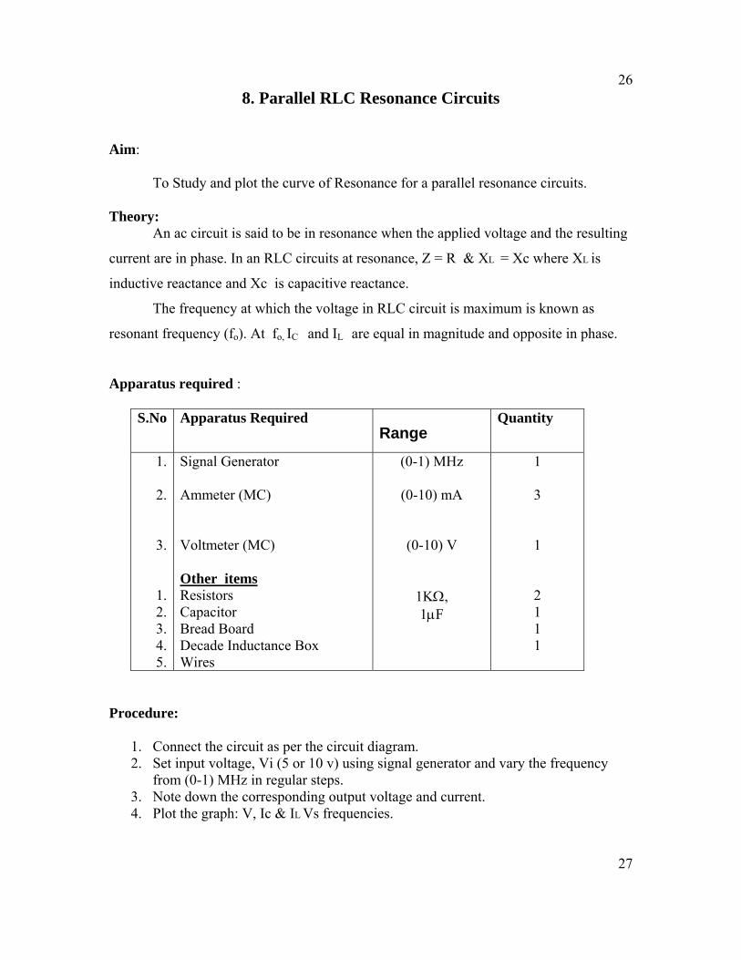
To Measure the Resonance Frequency
1. Plot the graph: Voltage Vs Frequencies 2. Draw a vertical line, from the maximum current reading to the X-axis. That is the resonant frequency f0.
Circuit Diagram:
MODEL GRAPHS:
28
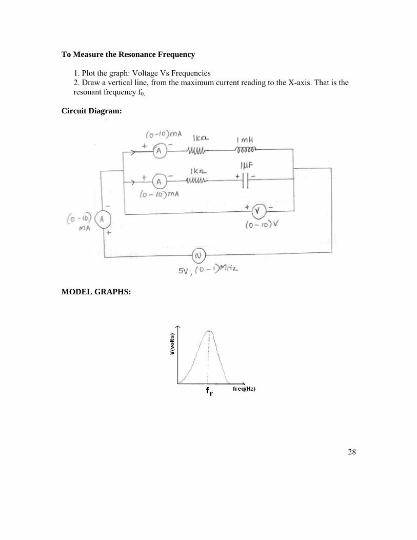
Observation: Vin= 5 V
Frequency (KHz) Voltage
Vr(volts) Current (mA) IL IC
100KHz 200KHz 300KHz . . . . 1MHz
Theoretical Calculation:
fr = 1 /(2 Π√LC) Hertz where, fr = Resonant frequency L = Inductance
C = Capacitance
Result
Thus the resonance curve for parallel resonance is plotted and verified the resonant frequency.
29
9. Series RLC Resonance Circuits
Aim:
To Study and plot the curve of Resonance for a Series resonance circuits. Theory:
An ac circuit is said to be in resonance when the applied voltage and the resulting
current are in phase. In an RLC circuits at resonance, Z = R & XL = Xc where XL is
inductive reactance and Xc is capacitive reactance.
The frequency at which the voltage in RLC circuit is maximum is known as
resonant frequency (fo). At fo IC and IL are equal in magnitude and opposite in phase.
Apparatus Required :
S.No Apparatus Required Range
Quantity
1.
2.
3.
1. 2. 3. 4. 5.
Signal Generator Ammeter (MC) Voltmeter (MC) Other items Resistors Capacitor Bread Board Decade Inductance Box Wires
(0-1) MHz
(0-10) mA
(0-10) V
1KΩ, 1μF
1 1 3 1 1 1 1
Procedure:
1. Connect the circuit as per the circuit diagram. 2. Set input voltage, Vi (5 or 10 v) using signal generator and vary the frequency
from (0-1)MHz in regular steps. 3. Note down the corresponding output voltage and current. 4. Plot the graph: I ,Vc & VL Vs frequencies.
30
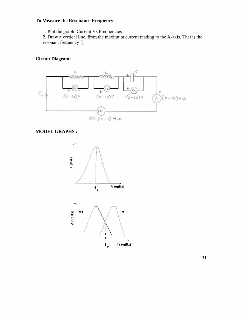
To Measure the Resonance Frequency:
1. Plot the graph: Current Vs Frequencies 2. Draw a vertical line, from the maximum current reading to the X-axis. That is the resonant frequency f0.
Circuit Diagram:
MODEL GRAPHS :
31
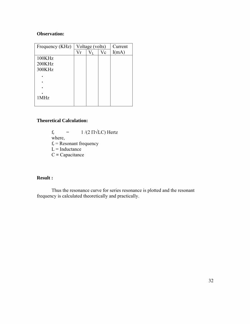
Observation: Frequency (KHz) Voltage (volts) Current
I(mA) Vr VL Vc 100KHz 200KHz 300KHz . . . . 1MHz
Theoretical Calculation:
fr = 1 /(2 Π√LC) Hertz where, fr = Resonant frequency L = Inductance
C = Capacitance
Result :
Thus the resonance curve for series resonance is plotted and the resonant frequency is calculated theoretically and practically.
32
10. POWER FACTOR MEARUREMENT
Aim To measure the real power, reactive power, power factor and impedance of the given RL and RC circuits. Theory:
• Impedance is the total measure of opposition to electric current and is the
complex (vector) sum of (“real”) resistance and (“imaginary”) reactance.
• Power is defined as the rate of flow of energy past a given point.
• In alternating current circuits, energy storage elements such as inductors and
capacitors cause periodic reversals of energy flow. The portion of power flow
averaged over a complete cycle of the AC waveform that results in net transfer of
energy in one direction is known as real power.
• The portion of power flow due to stored energy which returns to the source in
each cycle is known as reactive power.
• The ratio between real power and apparent power in a circuit is called the power
factor. Where the waveforms are purely sinusoidal, the power factor is the cosine
of the phase angle (φ) between the current and voltage sinusoid waveforms
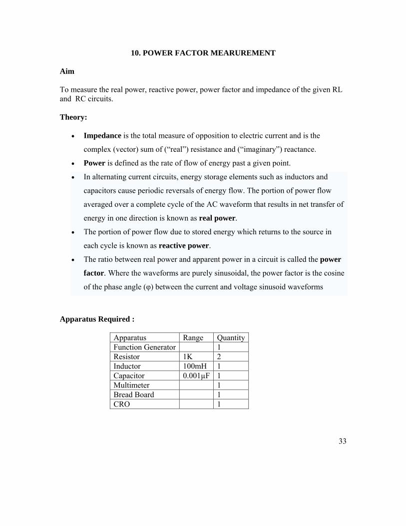
Apparatus Required :
Apparatus Range QuantityFunction Generator 1 Resistor 1K 2 Inductor 100mH 1 Capacitor 0.001µF 1 Multimeter 1 Bread Board 1 CRO 1
33

34
PROCEDURE
1. Give the connections as per the circuit diagram. 2. Connect the CRO probe at point A to get voltage waveform and at B to get the
current waveform. 3. Adjust vertical deflection of each channel such that the waveform fills the whole
screen. 4. Adjust the sweep rate and the horizontal position control until one half cycle of
the waveform spans 9 divisions on the scope’s scale. 5. Since one half cycle covers 9 divisions, it means each major division on the scope
represents 200. 6. Since each major division consists of 5 smaller divisions, each smaller division
represents 20/5 = 40. 7. Phase difference between two waveforms is determined by simply counting the
number of small divisions between corresponding points on the 2 waveforms. 8. Phase Angle φ = (no.of divisions) * ( degree / divisions). 9. Power Factor is given by Cos φ.
FORMULAS:
1. Real Power (P) = V* I Cos φ 2. Reactive Power (Q) = V* I Sin φ
3. Power Factor (P.F) = Cos φ = R / Z 4. Impedance (Z) = R / Cos φ
RESULT:
Thus the real power, reactive power, power factor and impedance of the given RLC circuit have been measured.
35