Embed Size (px)
Citation preview

1
E0-286 “VLSI Test”
1. Delay Test: LOC,LOS,PD,SDD. Delay test with multiple-clock domains. Scan architectures to improve delay test coverage. Testing memory interface logic

2
At-speed test
q Stuck-at tests ensures that the manufactured design meets the functionality, based on structural fault coverage
q At-speed tests ensures that the manufactured design meets the timing constraints, based on structural fault coverage¦ Timing constraints: setup and hold
q How many (at-speed) capture clock pulses are needed to test a design for setup timing compliance…¦ for a full-scan design?¦ for a partial-scan design?
q How many clock pulses are needed to test a design for hold timing compliance…¦ for a full-scan design?¦ for a partial-scan design?

3
Fault models for testing setup delay defects
q Path delay fault model: Delay defect in a circuit may result in cumulative delay of a combinational path to exceed the specified duration (or the clock period).¦ Number of potential fault sites = number of paths.
? Path start (end) point: output (capture input) of a scan flip-flop? Number of paths may be exponential with number of gates!
¦ Fault: Path and its transition direction
q Transition delay fault model: Delay defect at gate terminals is assumed to be large enough to prevent any passing transition through the gate from reaching any output within the specified duration (or the clock period).¦ Number of potential fault sites = number of gates¦ Fault: slow-to-rise (str) and slow-to-fall (stf) at gate terminals

4
q Two pattern tests enough to target setup in a testable full-scan circuit: V1 à V2
q V1 is initialisation pattern => initializes the state.
q V2 is launch pattern => launches a transition¦ Limitation is in generation of launch pattern from initialization
pattern.
q Capture cycle then captures the result of launch pattern
q At-speed requirement is between launch pattern (V2) and capture pattern.¦ Initialization and launch may or may not be at-speed.
Scan-based setup delay fault tests

5
5-valued algebra
q S0 (S1): Steady 0 (1); V1 = V2 = 0 (1)
q U0 (U1): Final value is 0 (1); V1 = X, V2 = 0 (1)¦ V1 may be either 0 or 1¦ U0 = S0 OR (Fall)
q XX: V1 = V2 = X (don’t-care)
q Algebra:¦ S1.U0 = U0; U0.U1 = U0; …¦ S0+U1= U1; U0+U1 = U1; …¦ ~U0 = U1; …
q ATPG may use such algebra to generate robust / non-robust tests as required.¦ Robust test requires only Rise or Fall along the path.

6
Robust path-delay test
q Guarantees detection irrespective of delays in other parts of circuit.
f3
f5
f4
f8
f7
f6
f1
f0
f2
f9
a1
a0y0
y1
y2
y3
1
1
1
1
1
One fault is targetedper-pattern.
Disjoint path tests may be merged in samepattern
FF
F
F

7
Non-robust path-delay test
q Guarantees detection only when no other path-delay fault is present.
f3
f5
f4
f8
f7
f6
f1
f0
f2
f9
a1
a0y0
y1
y2
y3
Fault-free Faulty
a1
a0
y3
Strobe-points
U1
U1
U1
U1
U0
U0
U0F
U1

8
Transition delay fault test
q Transition at fault site and final value (V2) should be observed at output. Example: slow-to-fall @ f6
Any path may be usedfor justification and propagation.
Initial value is not observed.
f3
f5
f4
f8
f7
f6
f1
f0
f2
f9
a1
a0y0
y1
y2
y3
U1
U1
U1
F
U1
U1U1
U1
F

9
Stuck-at vs. Transition fault tests
q How many test patterns are required for the following circuit?
f1
f0 f9
f8
f7
f6
f3
f2
f5
f4
f1
f0 f9
f8
f7
f6
f3
f2
f5
f4
11
11
1
1
1
R
11
1
1
1
R
Stuck-at Test Example Transition Fault Test Example
Can this be generalized?

10
Small Delay Defects
0
5
10
4 8 12 16 20 24 28 32 36 40 44
Slack
Nod
es
Earlier metric:
• # transition faults detected.
New metric:
• # transition faults detected weighted as:
• (Fault * Minimal slack) / (Slack along detected path)
• Area under the slack curve.
q Take all patterns for a given slack – accept coverage obtained.
q Take all patterns for a given coverage – accept slack used.
% of detection path slack w.r.t. minimum path slack
Pattern count Coverage
10% 20% 30% 40% 50% 60% 10% 20% 30% 40% 50% 60%% of detection path slack w.r.t.
minimum path slack

11
q Ideally, V2 should be independently generated from V1 to enable applying any possible pattern to the DUT. ¦ This may require special hardware (i.e. hold-scan flip-flops)
q Otherwise, three possible ways to generate launch (V2), after initialization (V1)¦ LOS: V2 is shifted value of V1 (combinational). Different V2 for all V1 guaranteed.¦ LOC: V2 is functional state of V1 (sequential). Different V2 for all V1 not guaranteed.¦ LOC: V2 is functional state of V1 after many cycles. Higher number of launch states
(V2) for a given V1.
Scan-based transition fault tests
shift_in (LOS) shift_outlaunch
capture
Launch off shift
Launch off capturescan_enable
scan_enable
V1 V2
shift_in (LOC)

12
LOS vs. LOC
q LOS¦ Trivial to generate V2 from V1.
? Faster ATPG¦ Large number of parallel transitions possible => many faults
detectable per pattern ? Lesser pattern count.
¦ V2->capture is at-speed => SE switches at-speed? SE drives all flops like clock. At-speed SE => similar physical design
considerations like clock.¦ Scan chain ordering impacts coverage as different scan order
results in different V2 for a given V1.q LOC
¦ Sequential simulation required to generate V2 from V1? Time-consuming ATPG
¦ V2 is functionally reachable state from V1 => Multiple arbitrarytransitions may not be justifiable? Higher pattern count.
¦ No at-speed requirement on SE and no dependence on scan order

13
Improving limitations of LOS and LOC
q LOS requires at-speed scan enable¦ Pipelined scan enable addresses this to generate local at-speed SE.¦ For full-scan designs with no-sequential feedback, bi-partitioning
provides full LOS coverage with 2 slow-speed scan enables.
q Many techniques have been proposed to combine the best worlds of LOC and LOS to improve coverage¦ LOS by definition has N shifts and 1 capture.
? Last flop in each scan chain may not see a valid transition. ? LOES (launch on extra shift) addresses this.
¦ Scan enable partitioning techniques with multiple scan enables.¦ Combining multiple scan enables with multiple capture depths.
GSELSE GSE
LSE

14
Bi-partitioned scan
Phase-I- Launch fromblue.
- Capture in red.
Phase-II- Launch fromred.
- Capture in blue.
SE_R
SE_B
SE_B
SE_R
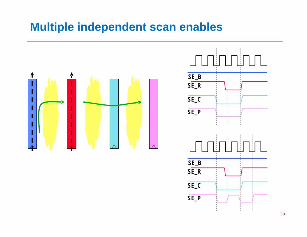
15
Multiple independent scan enables
SE_RSE_B
SE_C
SE_P
SE_RSE_B
SE_C
SE_P

16
Proof of coverage improvement
q Coverage improvement is directly related to the number of launch states (V2) possible for a given initialization state (V1)¦ V2(LOS) = S(V1), for all V1
¦ V2(LOC) = C(V1), for all V1
¦ V2(LOS+LOC) = S(V1)+C(V1), for all V1
¦ V2(2_SE) = SS(V1)+CC(V1)+SC(V1)+CS(V1), for all V1
Where S denote shift, C denotes capture
q Can this be generalized?

17
q Launch condition enabled through scan initialization (non-functional).
q Next state after scan shift is not necessarily functional. Depends on synthesis of next state functional. Very likely only reachable for incompletely state machines.
q Reachable ? Functional. Former depends upon synthesis. Latter depends upon specification. For a completely specified machine, the two are same.
q Launch-off capture and launch-off shift patterns can both have non-functional launch states.
Functional vs. scan states in transition faults

18
q Transition fault pattern does not necessarily cause a transition in the capture flip-flop.¦ 0->1 transition on S is a valid transition fault test for A = 1 and B =1->0.¦ Fault-free output does not change: 1->1. Faulty o/p: 1 -> 0.
q Path delay pattern: A transition in capture flip-flop is guaranteed. However, not necessarily through a valid path.
q Path delay tests can be robust (single launch transition), non-robust (other enabling launch transitions), functional sensitisable (other enabling paths). Considerations for multi-cycle paths and false paths.
q Multiple cycle launches may be required to achieve a functional launch state.
Desirable Transitions
AS Z = A.S + B.S’
BS’

19
Clocking considerations
q Capture with slow-speed tester clock¦ Use of two time-sets¦ Use of on-chip clock generation
q Handling multiple clock domains for capture¦ Intra-domain test is simple
? One clock domain of interest at a time works fine.
¦ Inter-domain test of synchronous clocks? Either launch or capture in each domain§ ATPG with 2 cycles is simple
? Both launch and capture in each domain § ATPG with 2 cycles is complex due to edge alignment and LOS/LOC.§ Multi-time-frame sequential ATPG needed
¦ Inter-domain interaction of asynchronous clocks may be false, with the use of synchronizers / FIFOs

20
Generating at-speed clocks
q At-speed clocks for capture interleaved with slow-speed shift clocks can be generated from¦ Tester – high-cost tester that generates such a
precision¦ On-chip PLL – this is more likely
q Leaking two at-speed clocks from on-chip PLL
PLLCLK
LEAKER
Shift clock
Ref clock
Slow shift + Fast capture
SE

21
Test time optimization with multiple clock domains
q Scan chain considerations with mixing multiple clocks: similar to mixing posedge and negedge flops
q Test time limitations with standard scan chains¦ Capture on one domain => wasted shift cycles on all
other domain? Shift-per-clock-domain for testing intra-domain faults
¦ Capture across multiple domains ? Sequential multi-cycle (>2) ATPG => run-time intensive? Simpler two-cycle ATPG§ Masking inter-domain logic for correctness
? Handling test power issues with minimal test time impact§ Staggered capture across domains

22Process Spread
Nor
mal
ized
Fm
ax
Testing logic-memory interface
q Control or observe flops do not exercise the true speed paths¦ Poor ATPG effectiveness though the coverage may be
good

23
Testing logic-memory interface
q Scan-enable partitioning can be extended here as well¦ RAM-sequential ATPG for logic->memory paths
? Q fault RAM-sequential pattern: <load, W, W, R, R, C, unload>? Address fault RAM-sequential pattern: <load, W, W, R, C, unload>
¦ Generating transition becomes simpler with shift-only scan chains – similar to LOS
RAM
C
C
C
Q
ADR
D
ME
ADR
TADR
D
TD
ME
TME
Q
ATPG_MODE = 0BISTE = 0
F
F
F
F
B
F
F
F
B
F
Shift-onlyScan chain
CaptureScan chain

24
Testing memory-memory interface
q Need to exercise true memory paths during ATPG¦ Key idea: Maximal use of simpler non-functional (BIST or
shift) paths along non-targeted memory paths
@ M1: Wr.D1A1 Wr.
D2A2 Rd.A1
Rd.A2
Wr.CA Wr.
DB Rd.B@ M2:
Rd.A2
Capture1 2 3 4 5 6 7
M2
C
C
C
Q
ADR
D
ME
ADR
TADR
D
TD
ME
TME
Q
ATPG_MODE = 0BISTE = 0
F
F
F
F
B
F
F
F
B
M1
C
C
C
Q
ADR
D
ME
ADR
TADR
D
TD
ME
TME
Q
ATPG_MODE = 0BISTE = 1
B
B
B
B
B
B
B
B
B
B
B
B
Capture depth of 7 requiredfor M1 àM2 path
Can you generalizecapture-depth needed
for ‘M’ back-to-backmemories?

25
Hold delay ATPG
q A two-pattern ATPG <V1, V2> with one capture cycle¦ Slow capture clock is sufficient
q Path-delay fault model is simpler to translate setup path-delay patterns to hold path-delay patterns¦ Ensures that the path of interest (observing flip-flop)
has transition from one state to another
q Transition fault hold-delay patterns is not possible to be translated from setup-delay patterns¦ Transitions are not ensured at the observing flip-flop¦ Need to customized ATPG algorithm
? Similar as conventional setup delay, but one less clock pulse and launch state is observed.

26
Other references
q V. R. Devanathan: Novel Bi-partitioned Scan Architecture to Improve Transition Fault Coverage. Asian Test Symposium 2005.
q Hiroyuki Nakamura, et. al.: Low Cost Delay Testing of Nanometer SoCs Using On-Chip Clocking and Test Compression. Asian Test Symposium 2005.
q N. Ahmed, C.P. Ravikumar, M. Tehranipoor and J. Plusquellic: At-Speed Transition Fault Testing With Low Speed Scan Enable. VLSI Test Symposium 2005.
q V. R. Devanathan, C. P. Ravikumar, V. Kamakoti: Reducing SoC Test Time and Test Power in Hierarchical Scan Test : Scan Architecture and Algorithms. VLSI Design 2007.
q V. R. Devanathan, Srinivas Kumar Vooka: Techniques to improve memory interface test quality for complex SoCs. International Test Conference 2011.

27
Assignments
q Suggest a technique to achieve multiple independent at-speed scan enables for designs with only one slow-speed SE pin. (Hint: LOS)
q Express the total number of paths in the following circuit as a function of k?
q Would a test that detects str @ A also detect stuck-0 @ A? Similarly would a test for stuck-0 @ A also detect str @ A?
q For the circuit in slide 7, if the scan order is SI->f0->..fi->fi+1..->SO generate a test for str fault at output of f4 with LOC and LOS.
q For the below circuit what would be the worst-case capture depth to detect memory interface logic with the standard scheme? What if we use BIST paths?
M1 M2Q ADR QADR
M3ADR Q
M4ADR Q
M5ADR Q
M6ADR Q
TADR TD
BIST flop
Func.flop
Func.flop
BIST flop