Embed Size (px)
Citation preview
EE1411
ESD II A.A. 08/09
Dynamic CMOSDynamic CMOS
In static circuits at every point in time (except when switching) the output is connected to either GND or VDD via a low resistance path.
fan-in of n requires 2n (n N-type + n P-type) devices
Dynamic circuits rely on the temporary storage of signal values on the capacitance of high impedance nodes.
requires on n + 2 (n+1 N-type + 1 P-type) transistors
EE1412
ESD II A.A. 08/09
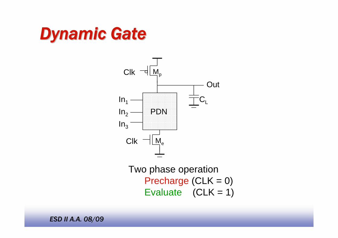
Dynamic GateDynamic Gate
In1
In2 PDNIn3
Me
Mp
Clk
ClkOut
CL
Two phase operationPrecharge (CLK = 0)Evaluate (CLK = 1)
EE1413
ESD II A.A. 08/09
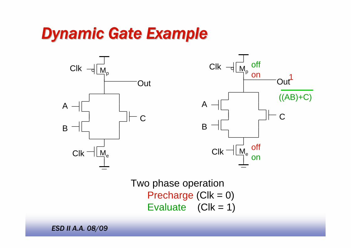
Dynamic Gate ExampleDynamic Gate Example
Out
Clk
Clk
A
BC
Mp
Me
Two phase operationPrecharge (Clk = 0)Evaluate (Clk = 1)
on
off
1off
on
((AB)+C)
Out
Clk
Clk
A
BC
Mp
Me
EE1414
ESD II A.A. 08/09
Conditions on OutputConditions on Output
Once the output of a dynamic gate is discharged, it cannot be charged again until the next precharge operation.Inputs to the gate can make at most one transition during evaluation.
Output can be in the high impedance state during and after evaluation (PDN off), state is stored on CL
EE1415
ESD II A.A. 08/09
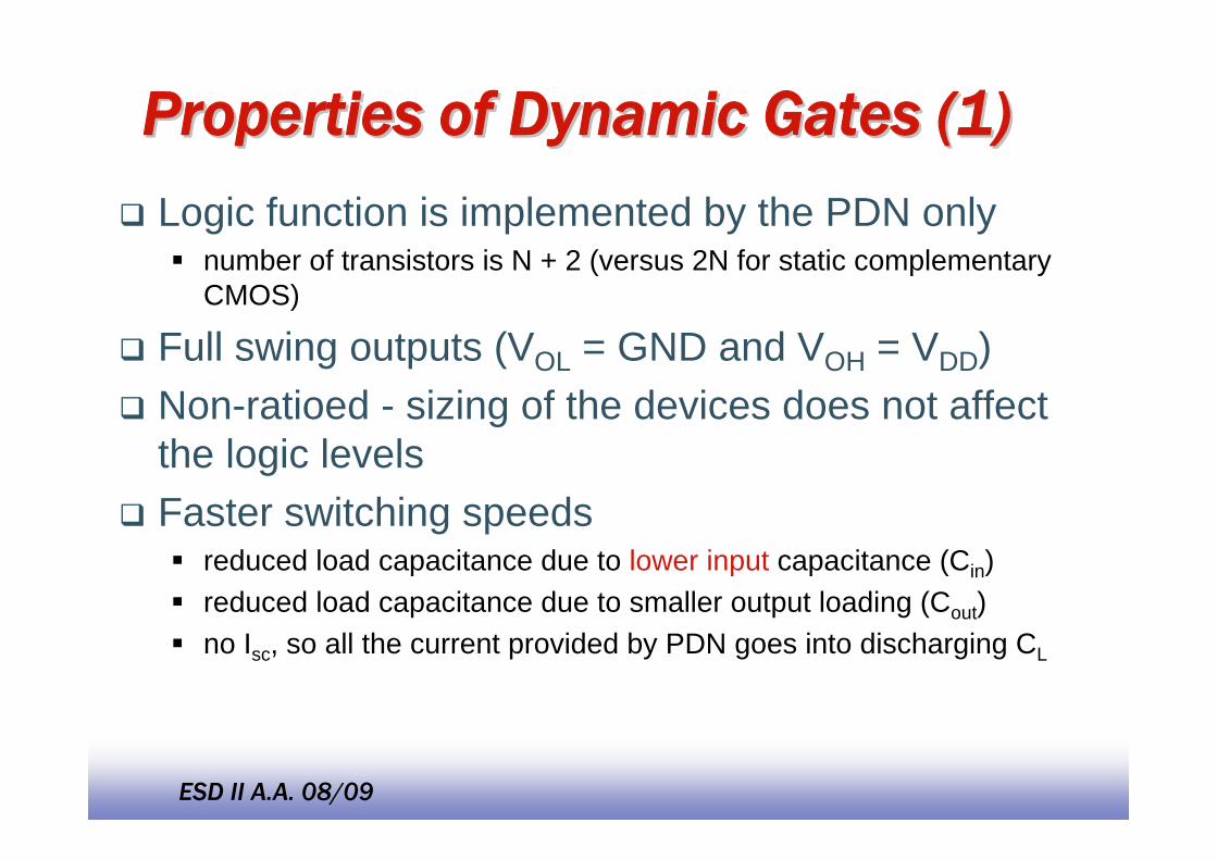
Properties of Dynamic Gates (1)Properties of Dynamic Gates (1)Logic function is implemented by the PDN only
number of transistors is N + 2 (versus 2N for static complementary CMOS)
Full swing outputs (VOL = GND and VOH = VDD)Non-ratioed - sizing of the devices does not affect the logic levelsFaster switching speeds
reduced load capacitance due to lower input capacitance (Cin)reduced load capacitance due to smaller output loading (Cout)no Isc, so all the current provided by PDN goes into discharging CL
EE1416
ESD II A.A. 08/09
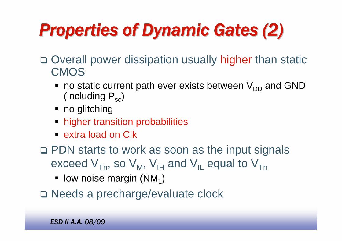
Properties of Dynamic Gates (2)Properties of Dynamic Gates (2)Overall power dissipation usually higher than static CMOS
no static current path ever exists between VDD and GND (including Psc)no glitchinghigher transition probabilitiesextra load on Clk
PDN starts to work as soon as the input signals exceed VTn, so VM, VIH and VIL equal to VTn
low noise margin (NML)Needs a precharge/evaluate clock
EE1417
ESD II A.A. 08/09
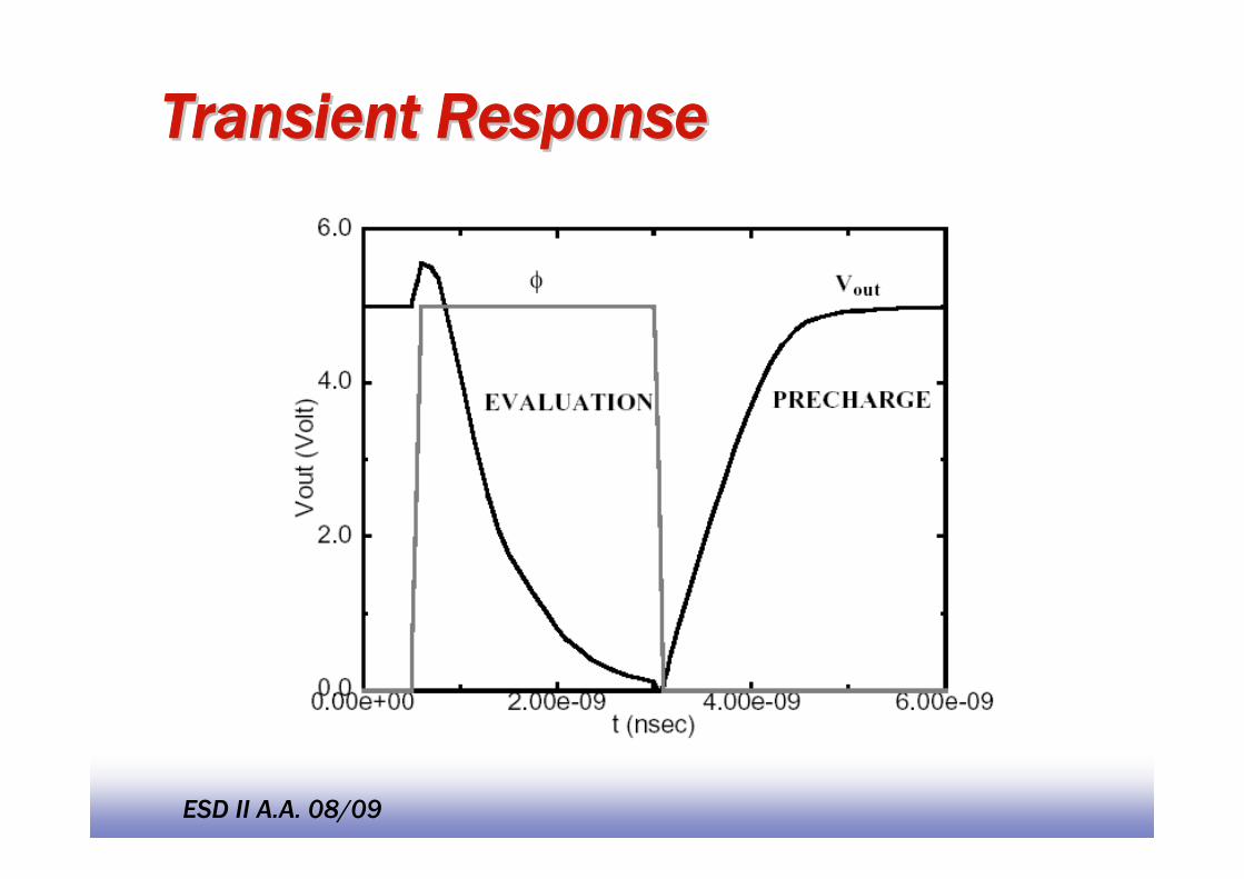
TransientTransient ResponseResponse
EE1418
ESD II A.A. 08/09
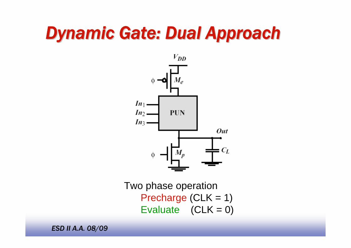
Dynamic Gate: Dual ApproachDynamic Gate: Dual Approach
Two phase operationPrecharge (CLK = 1)Evaluate (CLK = 0)
EE1419
ESD II A.A. 08/09
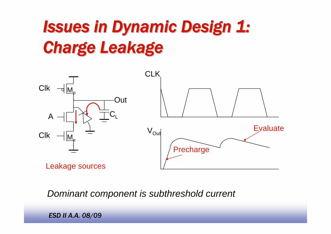
Issues in Dynamic Design 1: Issues in Dynamic Design 1: Charge LeakageCharge Leakage
CL
Clk
ClkOut
A
Mp
Me
Leakage sources
CLK
VOut
Precharge
Evaluate
Dominant component is subthreshold current
EE14110
ESD II A.A. 08/09
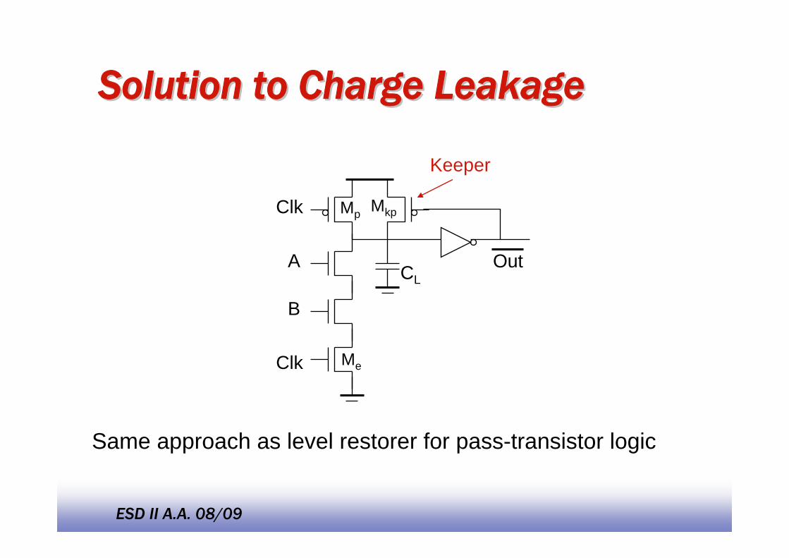
Solution to Charge LeakageSolution to Charge Leakage
Same approach as level restorer for pass-transistor logic
CL
Clk
Clk
Me
Mp
A
B
Out
Mkp
Keeper
EE14111
ESD II A.A. 08/09
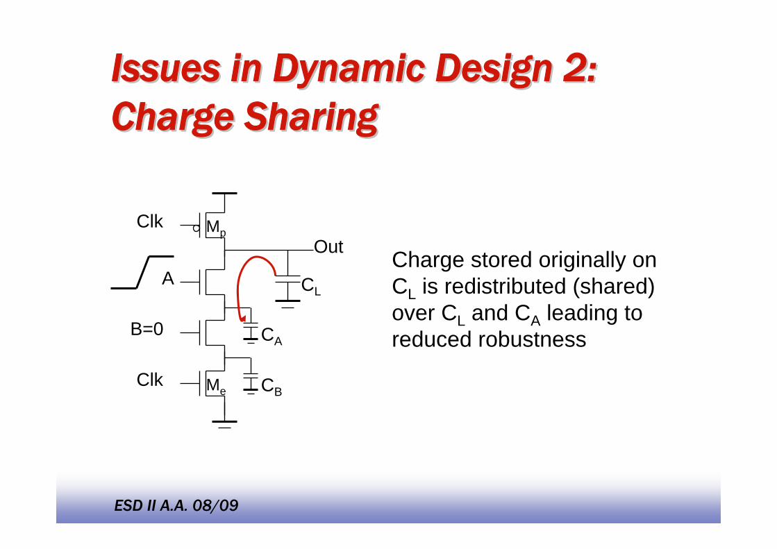
Issues in Dynamic Design 2: Issues in Dynamic Design 2: Charge SharingCharge Sharing
Charge stored originally on CL is redistributed (shared) over CL and CA leading to reduced robustness
CL
Clk
Clk
CA
CB
B=0
A
OutMp
Me
EE14112
ESD II A.A. 08/09
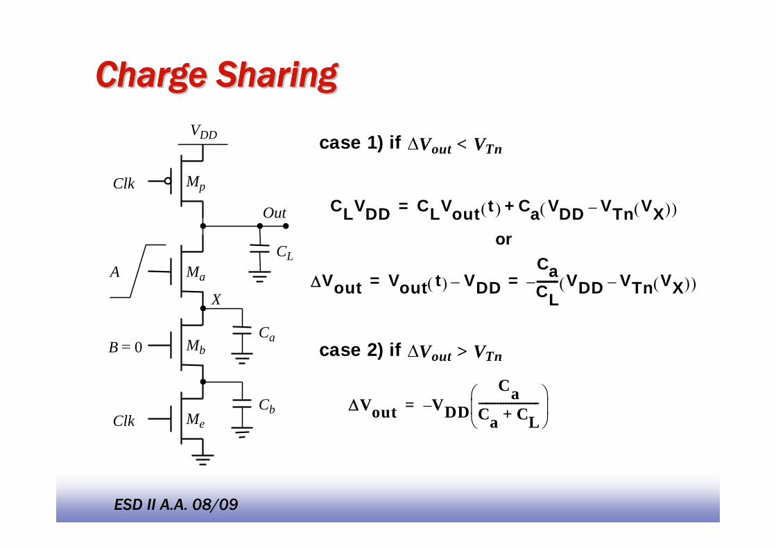
Charge SharingCharge Sharing
CLVDD CLVout t( ) Ca VDD VTn VX( )–( )+=
or
ΔVout Vout t( ) VDD–CaCL-------- VDD VTn VX( )–( )–= =
ΔVout VDDCa
Ca CL+----------------------⎝ ⎠⎜ ⎟⎛ ⎞
–=
case 1) if ΔVout < VTn
case 2) if ΔVout > VTnB = 0
Clk
X
CL
Ca
Cb
A
Out
Mp
Ma
VDD
Mb
Clk Me
EE14113
ESD II A.A. 08/09
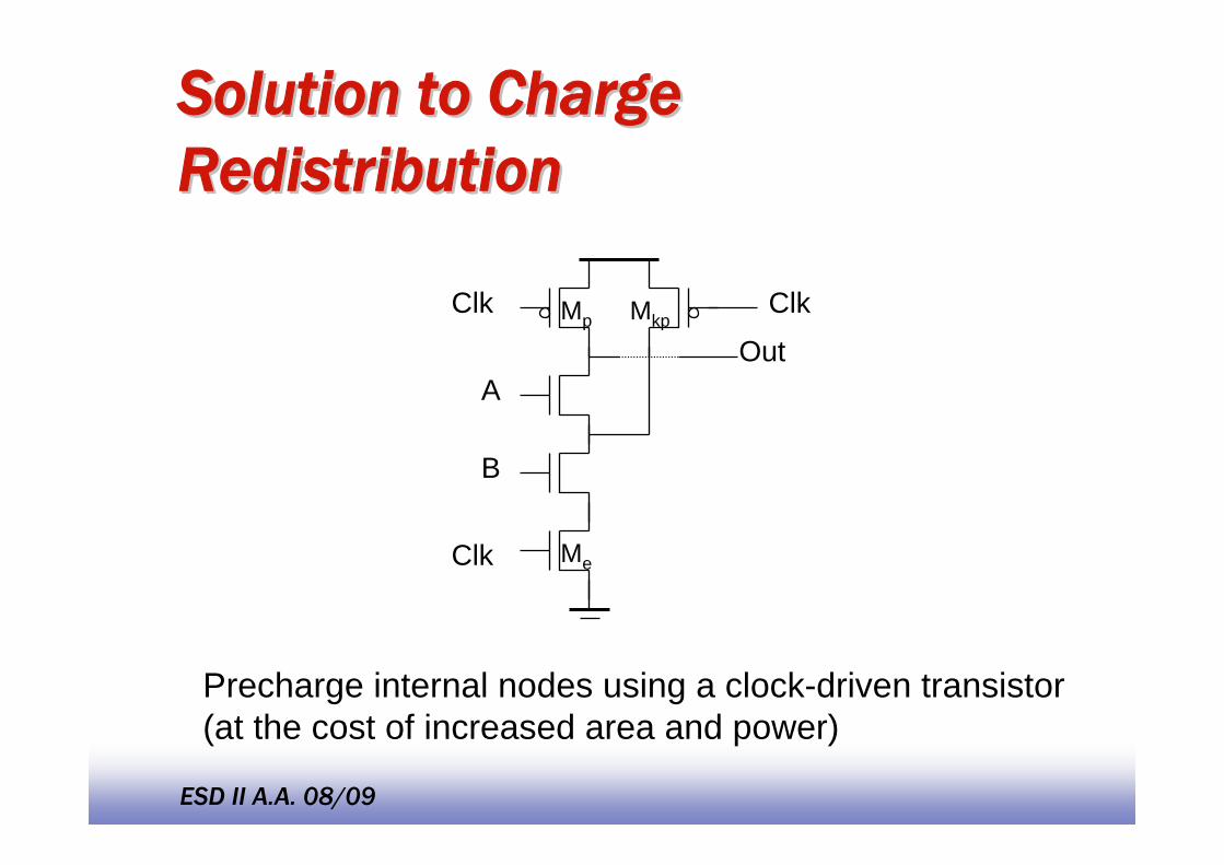
Solution to Charge Solution to Charge RedistributionRedistribution
Clk
Clk
Me
Mp
A
B
OutMkp
Clk
Precharge internal nodes using a clock-driven transistor (at the cost of increased area and power)
EE14114
ESD II A.A. 08/09
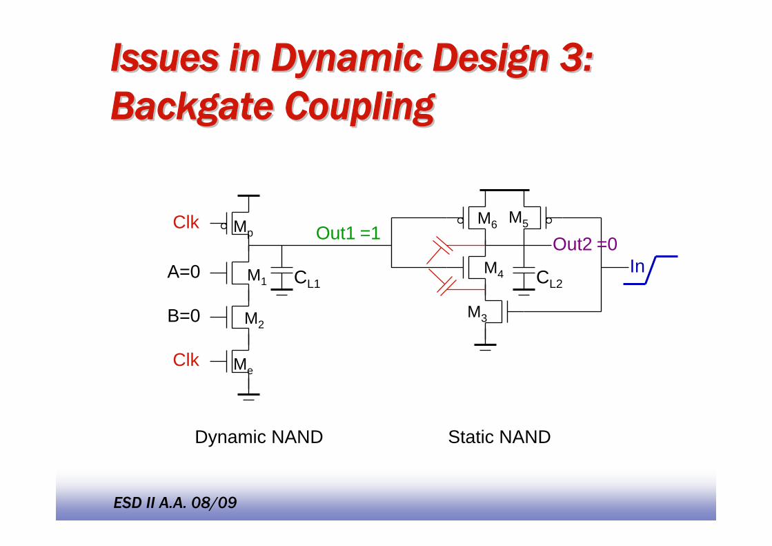
Issues in Dynamic Design 3: Issues in Dynamic Design 3: BackgateBackgate CouplingCoupling
CL1
Clk
Clk
B=0
A=0
Out1Mp
Me
Out2
CL2In
Dynamic NAND Static NAND
=1 =0M4
M3
M5M6
M1
M2
EE14115
ESD II A.A. 08/09
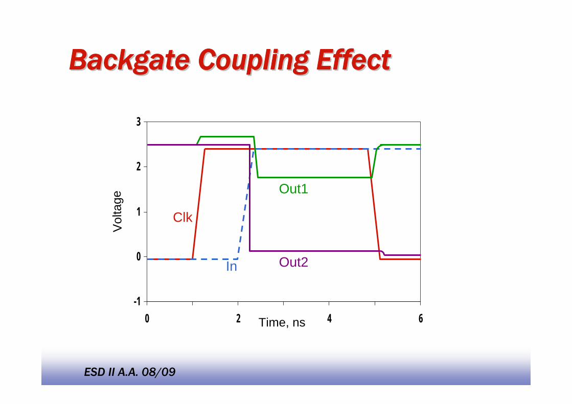
BackgateBackgate Coupling EffectCoupling Effect
-1
0
1
2
3
0 2 4 6
Vol
tage
Time, ns
Clk
In
Out1
Out2
EE14116
ESD II A.A. 08/09
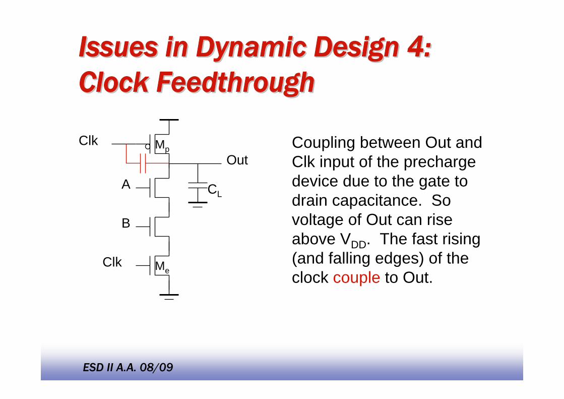
Issues in Dynamic Design 4: Issues in Dynamic Design 4: Clock Clock FeedthroughFeedthrough
CL
Clk
Clk
B
A
OutMp
Me
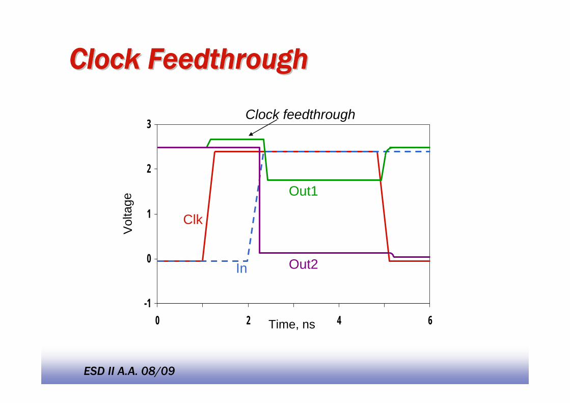
Coupling between Out and Clk input of the prechargedevice due to the gate to drain capacitance. So voltage of Out can rise above VDD. The fast rising (and falling edges) of the clock couple to Out.
EE14117
ESD II A.A. 08/09
Clock Clock FeedthroughFeedthrough
-1
0
1
2
3
0 2 4 6
Vol
tage
Time, ns
Clk
In
Out1
Out2
Clock feedthrough
EE14118
ESD II A.A. 08/09
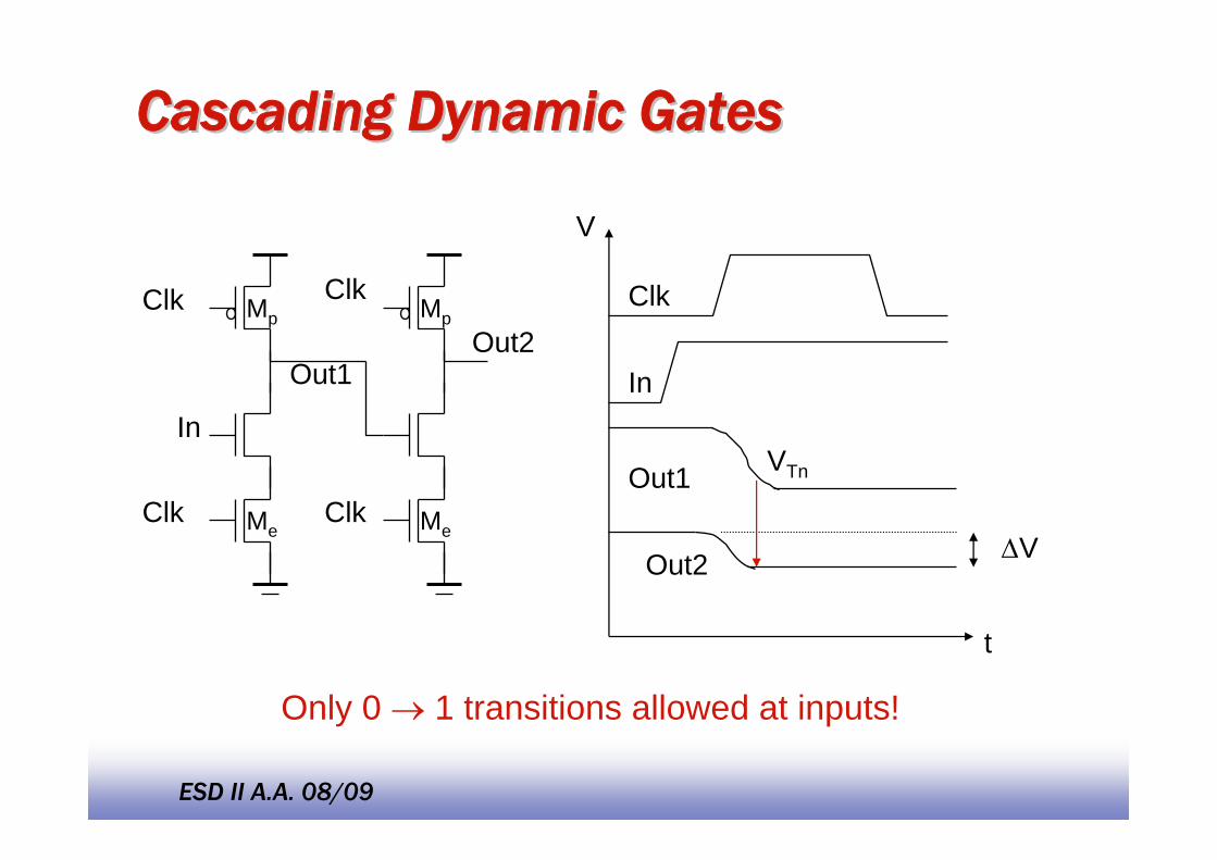
Cascading Dynamic GatesCascading Dynamic Gates
Clk
Clk
Out1
In
Mp
Me
Mp
Me
Clk
Clk
Out2
V
t
Clk
In
Out1
Out2 ΔV
VTn
Only 0 → 1 transitions allowed at inputs!
EE14119
ESD II A.A. 08/09
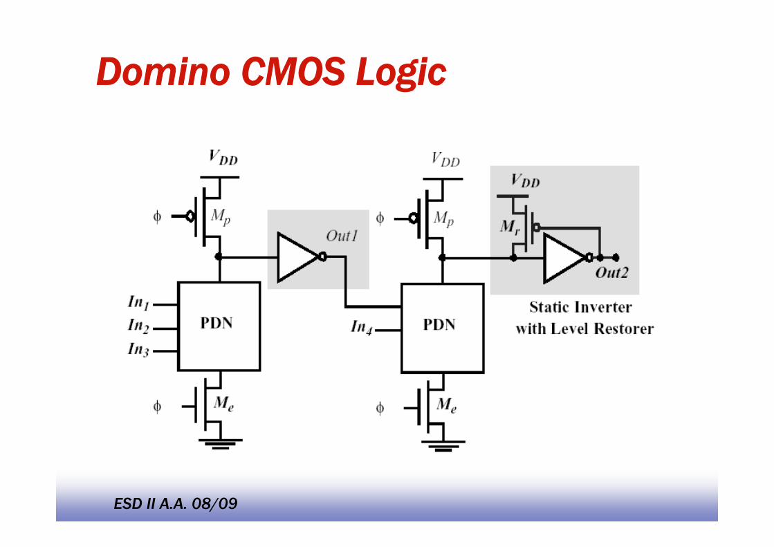
Domino CMOS Logic
EE14120
ESD II A.A. 08/09
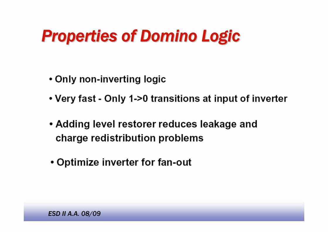
Properties of Domino LogicProperties of Domino Logic
EE14121
ESD II A.A. 08/09
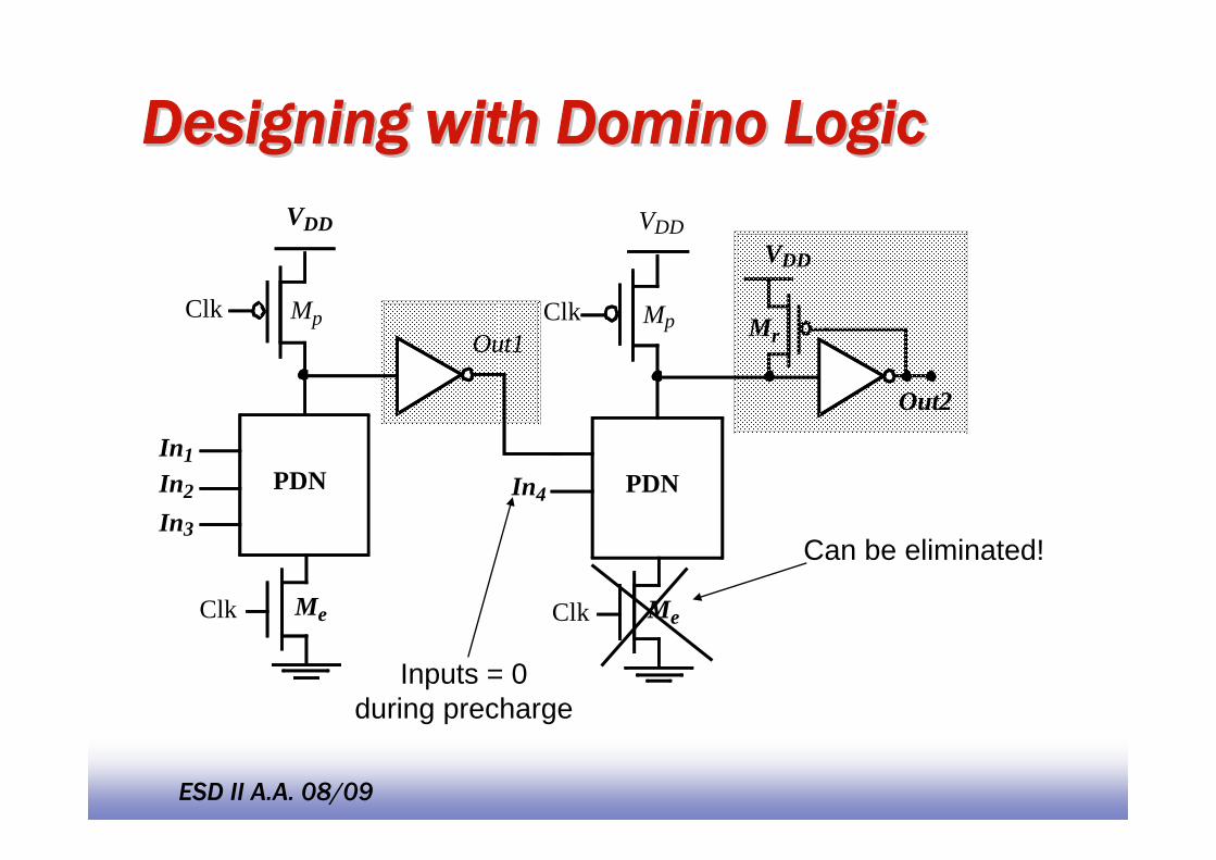
Designing with Domino LogicDesigning with Domino Logic
Mp
Me
VDD
PDN
Clk
In1In2
In3
Out1
Clk
Mp
Me
VDD
PDN
Clk
In4
Clk
Out2
Mr
VDD
Inputs = 0during precharge
Can be eliminated!
EE14122
ESD II A.A. 08/09
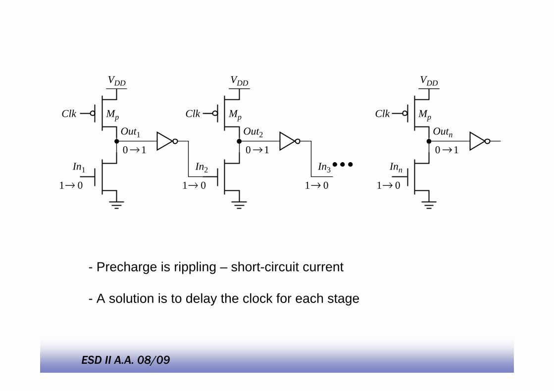
VDD
Clk Mp
Out1
In1
1 0
VDD
Clk Mp
Out2
In2
VDD
Clk Mp
Outn
InnIn3
1 0
0 1 0 1 0 1
1 0 1 0
- Precharge is rippling – short-circuit current
- A solution is to delay the clock for each stage
EE14123
ESD II A.A. 08/09
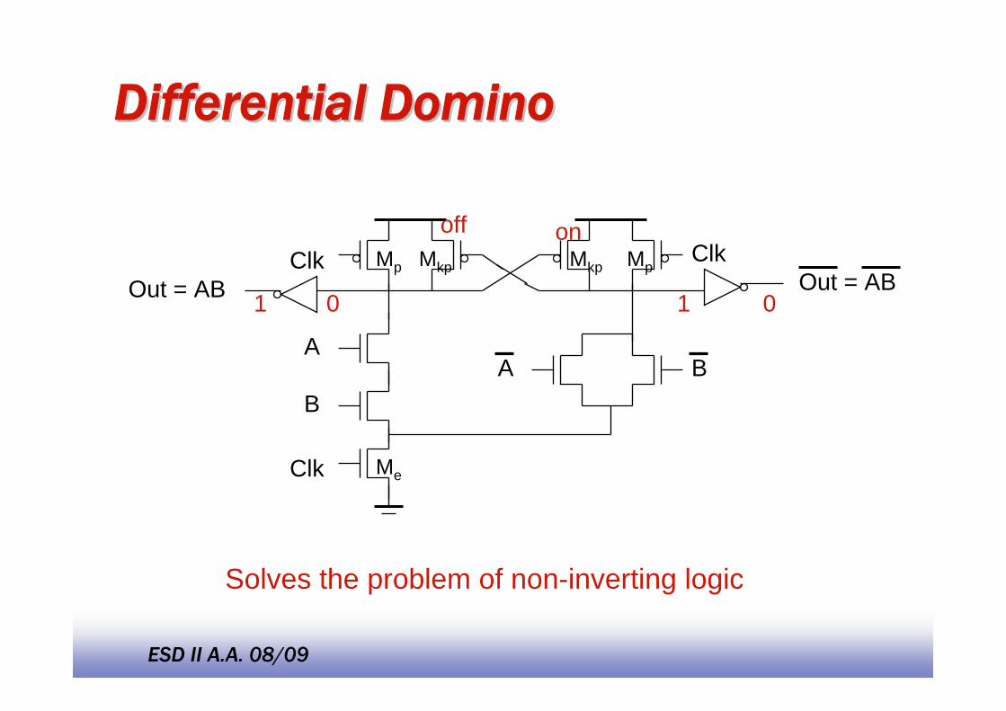
Differential DominoDifferential Domino
Solves the problem of non-inverting logic
A
B
Me
Mp
Clk
ClkOut = AB
A B
MkpClk
Out = ABMkp Mp
1 0 1 0
onoff
EE14124
ESD II A.A. 08/09
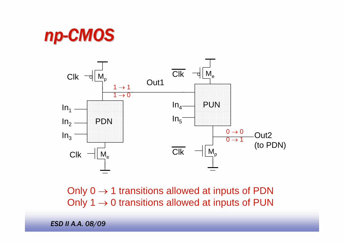
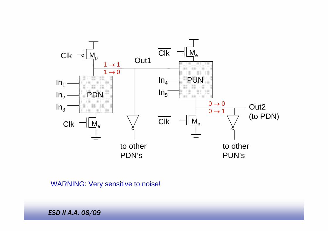
npnp--CMOSCMOS
Only 0 → 1 transitions allowed at inputs of PDN Only 1 → 0 transitions allowed at inputs of PUN
In1
In2 PDN
In3
Me
Mp
Clk
ClkOut1
In4 PUN
In5
Me
MpClk
Clk
Out2(to PDN)
1 → 11 → 0
0 → 00 → 1
EE14125
ESD II A.A. 08/09
WARNING: Very sensitive to noise!
In1
In2 PDNIn3
Me
Mp
Clk
Clk Out1
In4 PUNIn5
Me
MpClk
Clk
Out2(to PDN)
1 → 11 → 0
0 → 00 → 1
to otherPDN’s
to otherPUN’s