Embed Size (px)
Citation preview
EE1411
ESD II A.A. 08/09
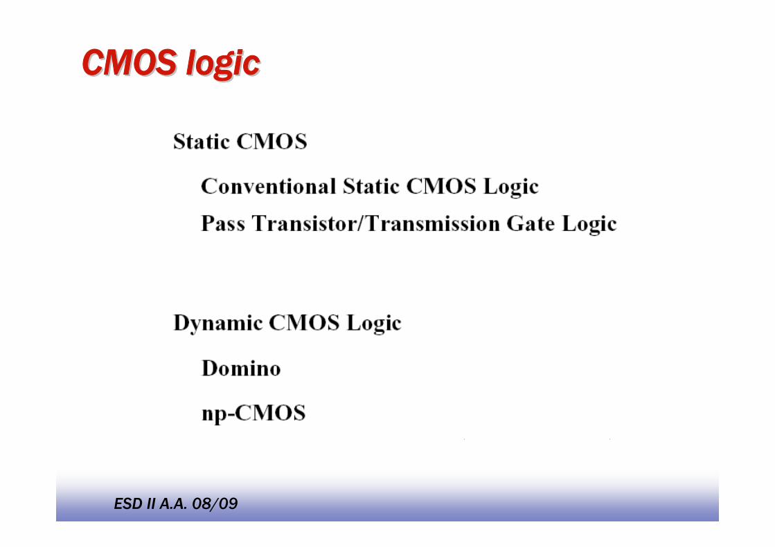
CMOS logicCMOS logic
EE1412
ESD II A.A. 08/09
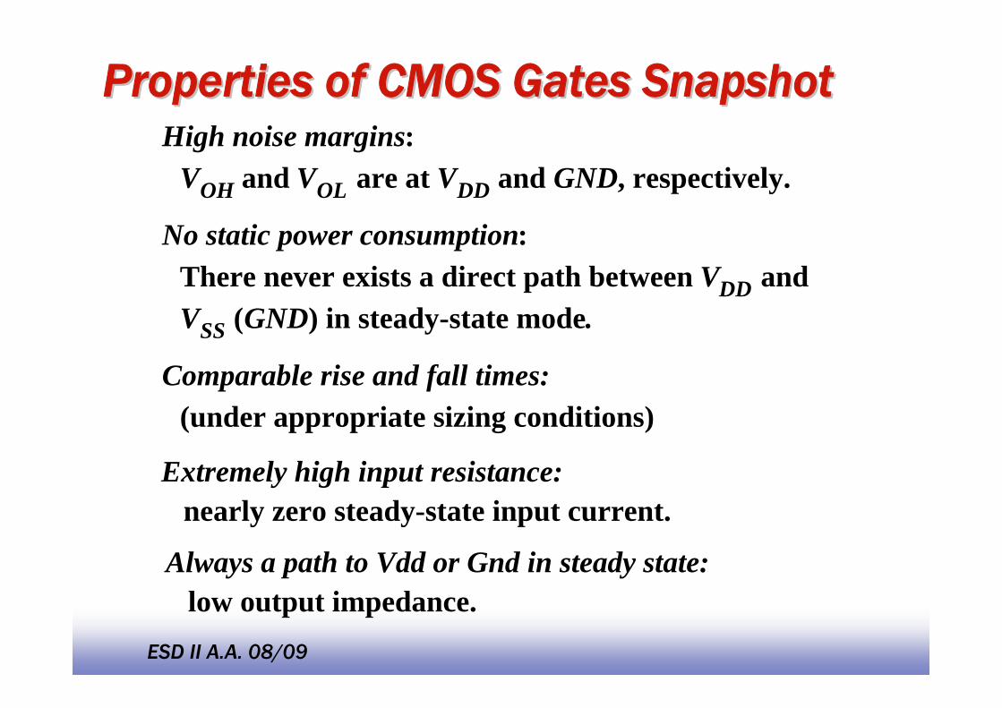
Properties of CMOS Gates SnapshotProperties of CMOS Gates SnapshotHigh noise margins:
VOH and VOL are at VDD and GND, respectively.
No static power consumption:There never exists a direct path between VDD and VSS (GND) in steady-state mode.
Comparable rise and fall times:(under appropriate sizing conditions)
Extremely high input resistance:nearly zero steady-state input current.
Always a path to Vdd or Gnd in steady state:low output impedance.
EE1413
ESD II A.A. 08/09
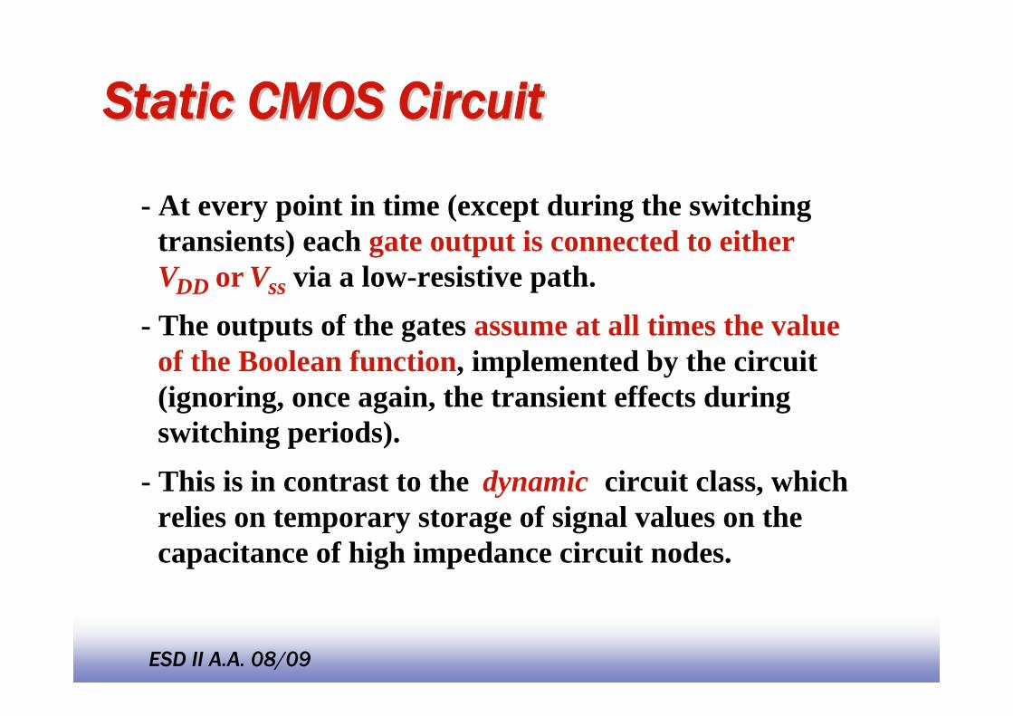
Static CMOS CircuitStatic CMOS Circuit
- At every point in time (except during the switching transients) each gate output is connected to eitherVDD or Vss via a low-resistive path.
- The outputs of the gates assume at all times the value of the Boolean function, implemented by the circuit (ignoring, once again, the transient effects during switching periods).
- This is in contrast to the dynamic circuit class, which relies on temporary storage of signal values on the capacitance of high impedance circuit nodes.
EE1414
ESD II A.A. 08/09
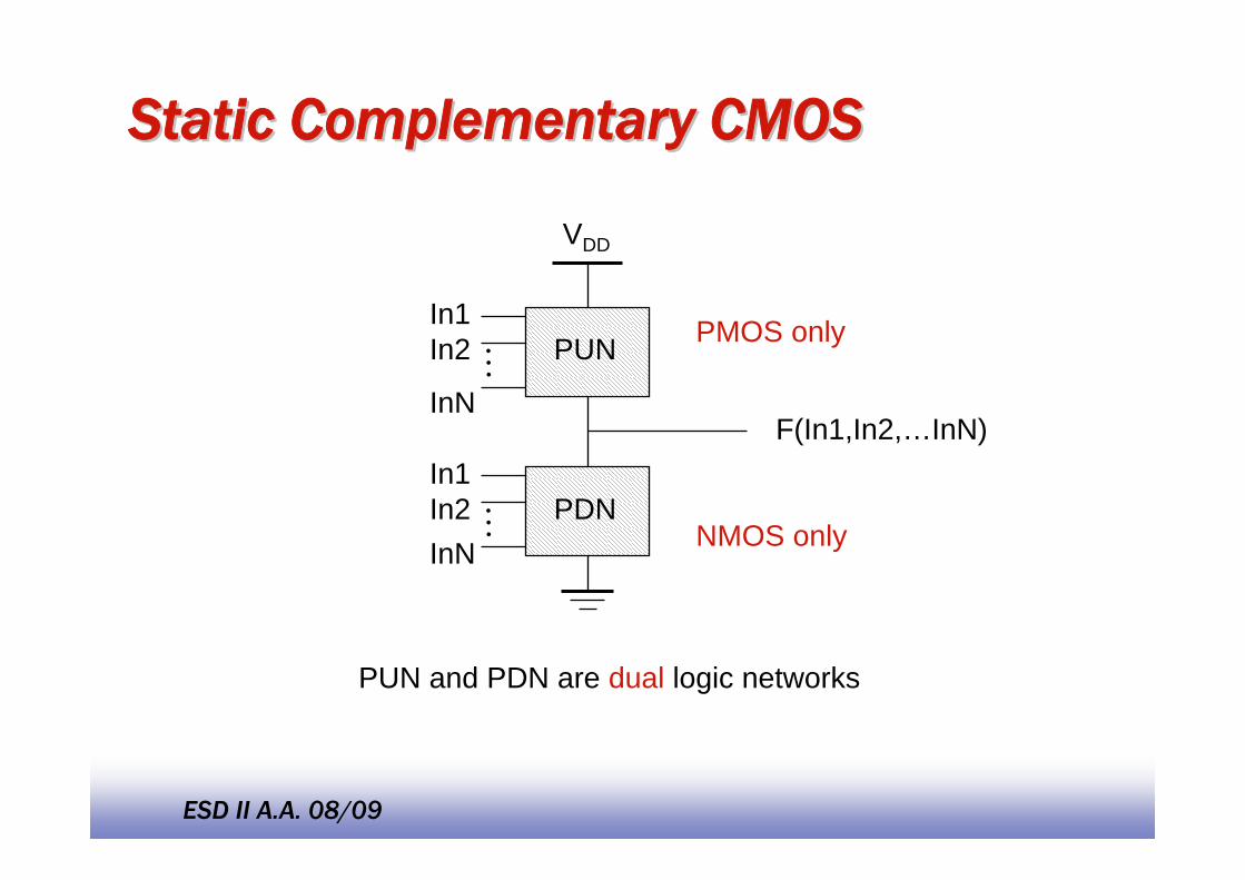
Static Complementary CMOSStatic Complementary CMOS
VDD
F(In1,In2,…InN)
In1In2
InN
In1In2InN
PUN
PDN
PMOS only
NMOS only
PUN and PDN are dual logic networks
……
EE1415
ESD II A.A. 08/09
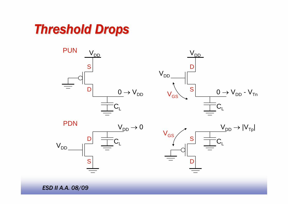
Threshold DropsThreshold DropsVDD
VDD → 0PDN
0 → VDD
CL
CL
PUN
VDD
0 → VDD - VTn
CL
VDD
VDD
VDD → |VTp|
CL
S
D S
D
VGS
S
SD
D
VGS
EE1416
ESD II A.A. 08/09
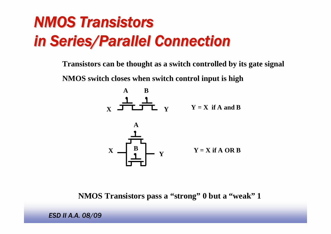
NMOS Transistors NMOS Transistors in Series/Parallel Connectionin Series/Parallel Connection
Transistors can be thought as a switch controlled by its gate signal
NMOS switch closes when switch control input is high
X Y
A B
Y = X if A and B
X Y
A
B Y = X if A OR B
NMOS Transistors pass a “strong” 0 but a “weak” 1
EE1417
ESD II A.A. 08/09
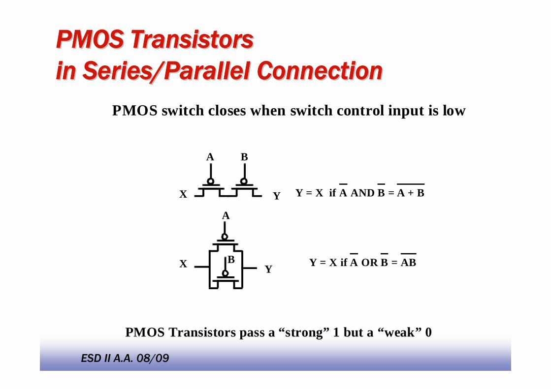
PMOS Transistors PMOS Transistors in Series/Parallel Connectionin Series/Parallel Connection
X Y
A B
Y = X if A AND B = A + B
X Y
A
B Y = X if A OR B = AB
PMOS Transistors pass a “strong” 1 but a “weak” 0
PMOS switch closes when switch control input is low
EE1418
ESD II A.A. 08/09
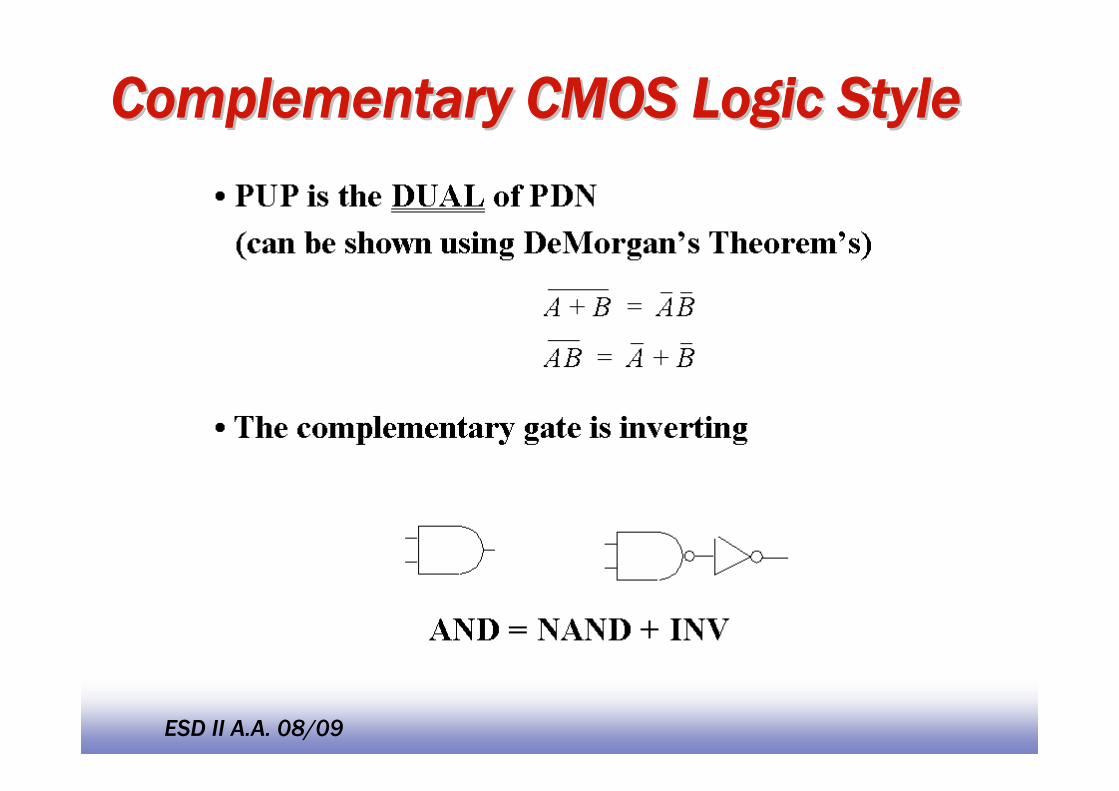
Complementary CMOS Logic StyleComplementary CMOS Logic Style
EE1419
ESD II A.A. 08/09
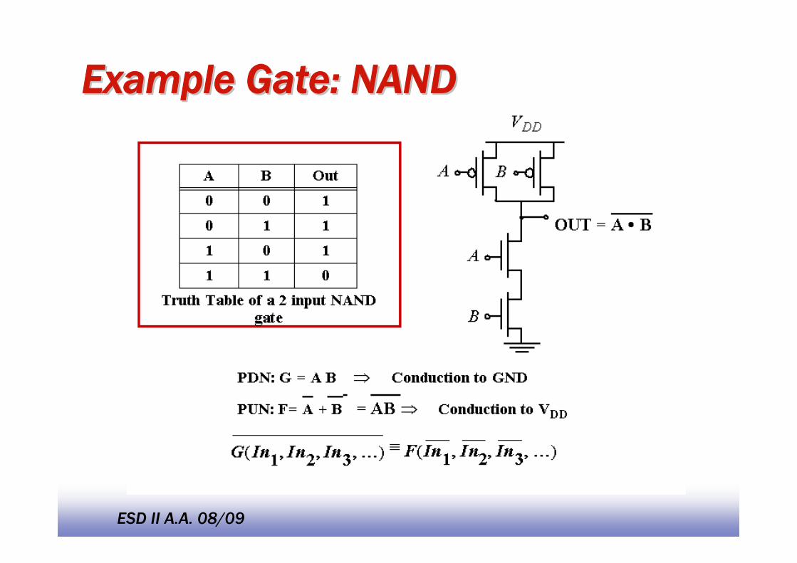
Example Gate: NANDExample Gate: NAND
EE14110
ESD II A.A. 08/09
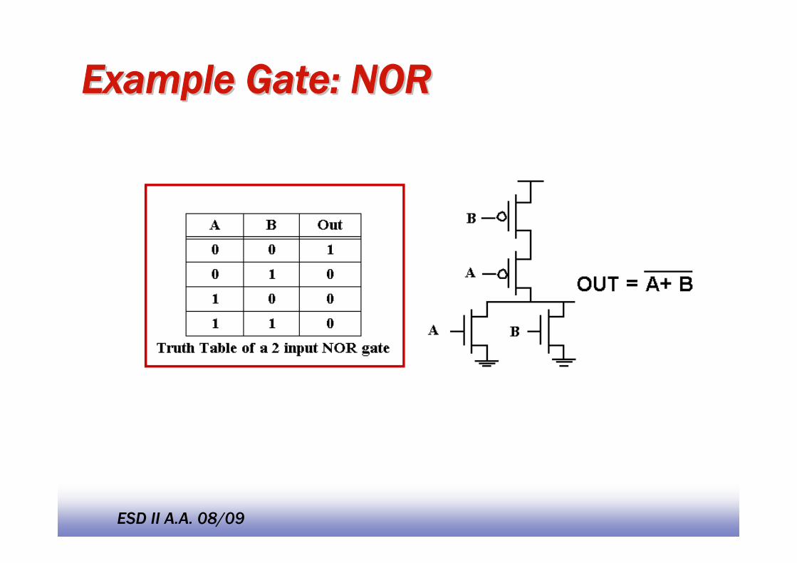
Example Gate: NORExample Gate: NOR
EE14111
ESD II A.A. 08/09
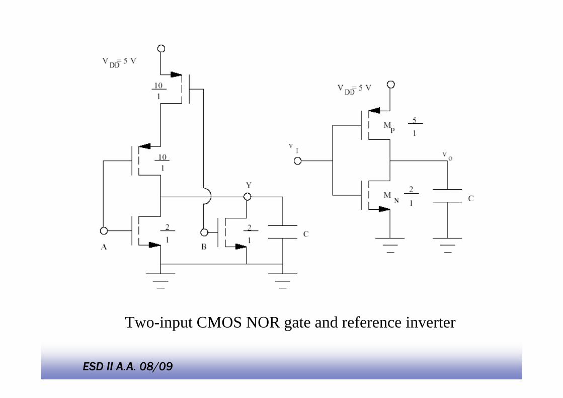
Two-input CMOS NOR gate and reference inverter
EE14112
ESD II A.A. 08/09
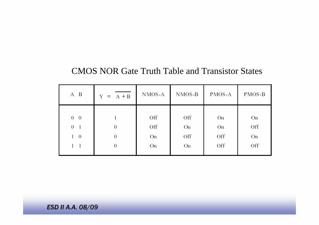
CMOS NOR Gate Truth Table and Transistor States
EE14113
ESD II A.A. 08/09
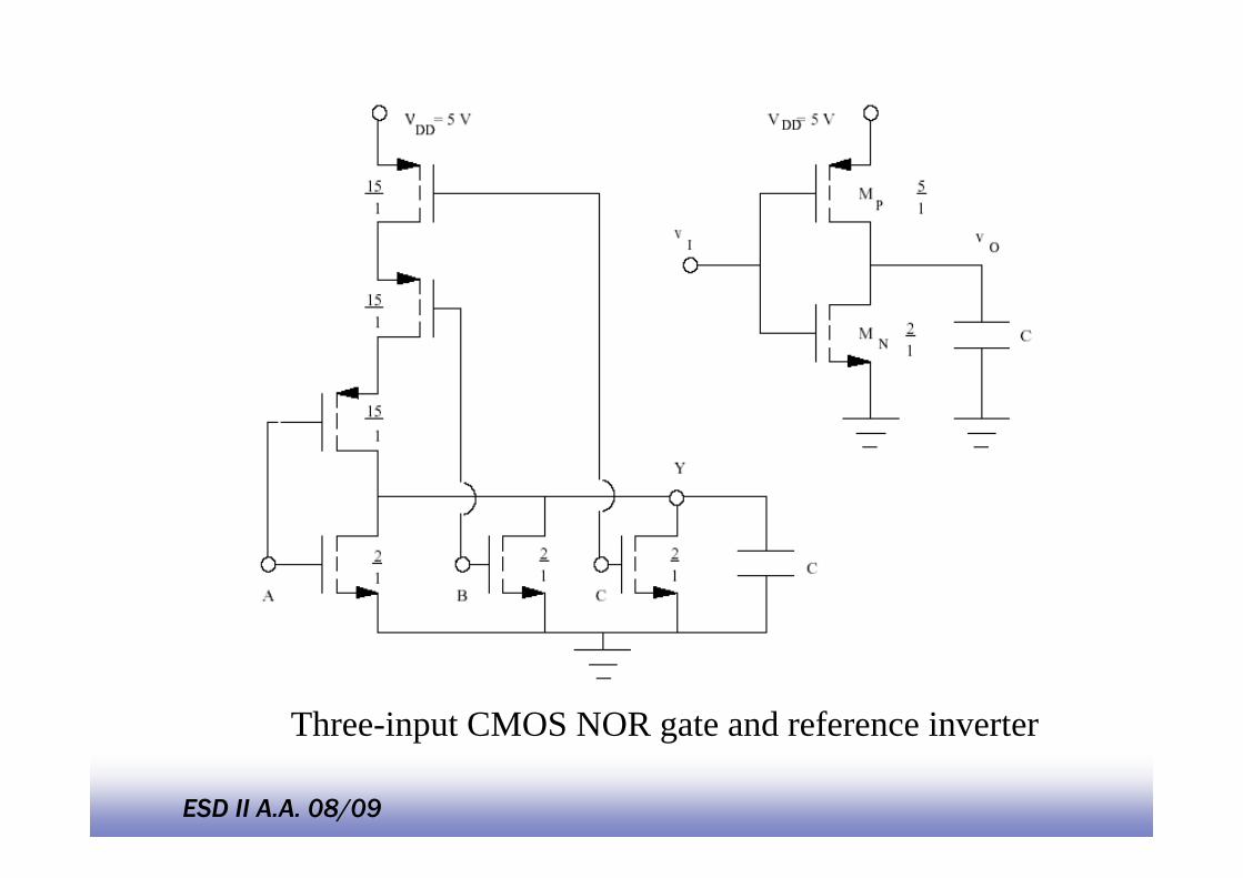
Three-input CMOS NOR gate and reference inverter
EE14114
ESD II A.A. 08/09
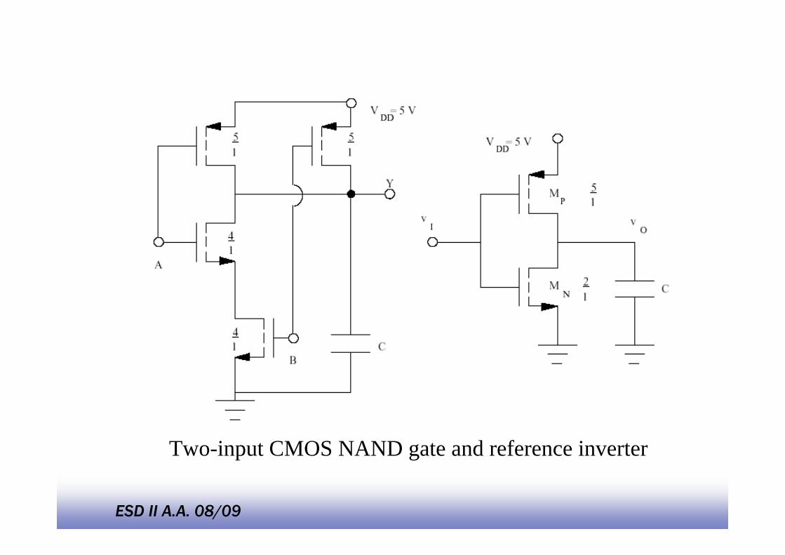
Two-input CMOS NAND gate and reference inverter
EE14115
ESD II A.A. 08/09
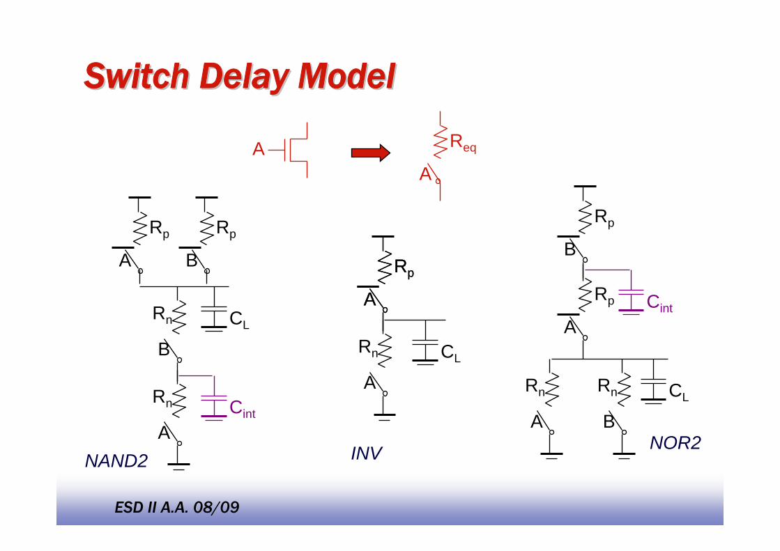
Switch Delay ModelSwitch Delay Model
A
Req
A
Rp
A
Rp
A
Rn CL
A
CL
B
Rn
A
Rp
B
Rp
A
Rn Cint
B
Rp
A
Rp
A
Rn
B
Rn CL
Cint
NAND2 INV NOR2
EE14116
ESD II A.A. 08/09
Input Pattern Effects on DelayInput Pattern Effects on Delay
Delay is dependent on the pattern of inputsLow to high transition
both inputs go low– delay is 0.69 Rp/2 CL
one input goes low– delay is 0.69 Rp CL
High to low transitionboth inputs go high
– delay is 0.69 2Rn CL
CL
B
Rn
A
Rp
B
Rp
A
Rn Cint
EE14117
ESD II A.A. 08/09
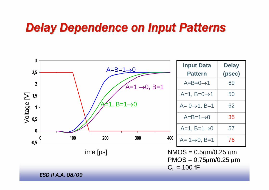
Delay Dependence on Input PatternsDelay Dependence on Input Patterns
-0,5
0
0,5
1
1,5
2
2,5
3
0 100 200 300 400
A=B=1→0
A=1, B=1→0
A=1 →0, B=1
time [ps]
Vol
tage
[V]
76A= 1→0, B=1
57A=1, B=1→0
35A=B=1→0
62A= 0→1, B=1
50A=1, B=0→1
69A=B=0→1
Delay(psec)
Input DataPattern
NMOS = 0.5μm/0.25 μmPMOS = 0.75μm/0.25 μmCL = 100 fF
EE14118
ESD II A.A. 08/09
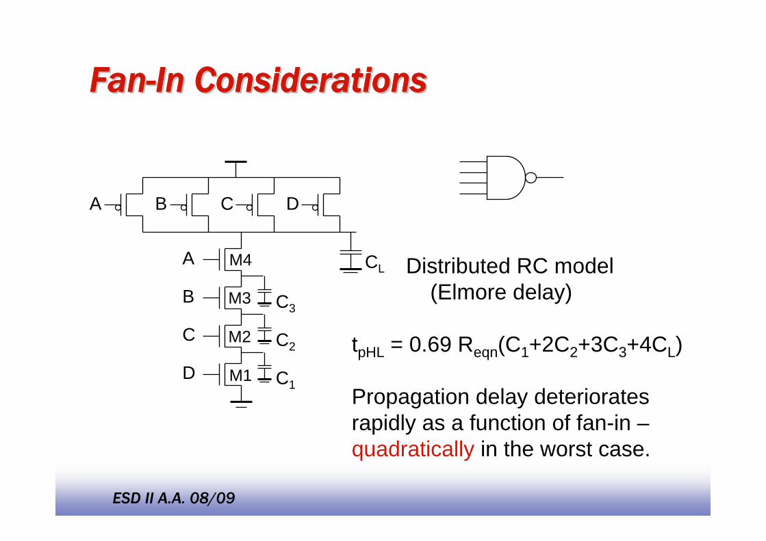
FanFan--In ConsiderationsIn Considerations
DCBA
D
C
B
A CL
C3
C2
C1
Distributed RC model(Elmore delay)
tpHL = 0.69 Reqn(C1+2C2+3C3+4CL)
Propagation delay deteriorates rapidly as a function of fan-in –quadratically in the worst case.
M1
M2
M3
M4
EE14119
ESD II A.A. 08/09
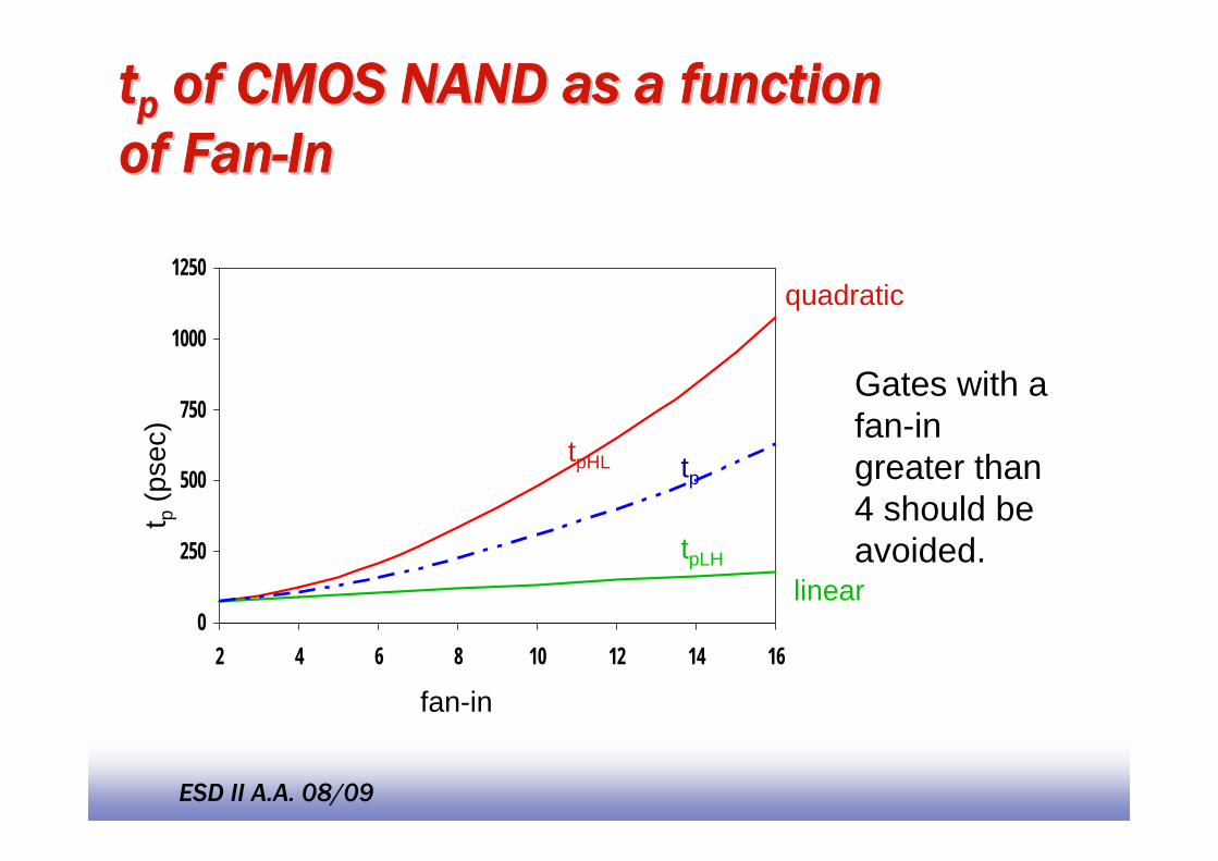
ttpp of CMOS NAND as a functionof CMOS NAND as a functionof Fanof Fan--InIn
0
250
500
750
1000
1250
2 4 6 8 10 12 14 16
tpHL
quadratic
lineartpLH
t p(p
sec)
fan-in
Gates with a fan-in greater than 4 should be avoided.
tp
EE14120
ESD II A.A. 08/09
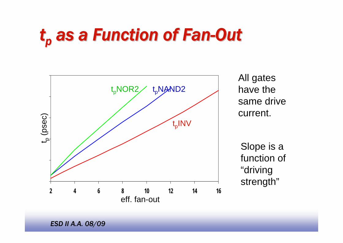
ttpp as a Function of Fanas a Function of Fan--OutOut
2 4 6 8 10 12 14 16
tpNOR2
t p(p
sec)
eff. fan-out
All gates have the same drive current.
tpNAND2
tpINV
Slope is a function of “driving strength”
EE14121
ESD II A.A. 08/09
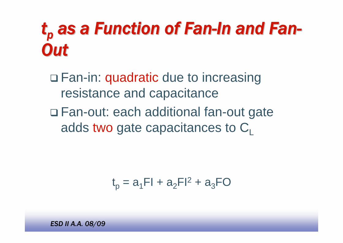
ttpp as a Function of Fanas a Function of Fan--In and FanIn and Fan--OutOut
Fan-in: quadratic due to increasing resistance and capacitanceFan-out: each additional fan-out gate adds two gate capacitances to CL
tp = a1FI + a2FI2 + a3FO
EE14122
ESD II A.A. 08/09
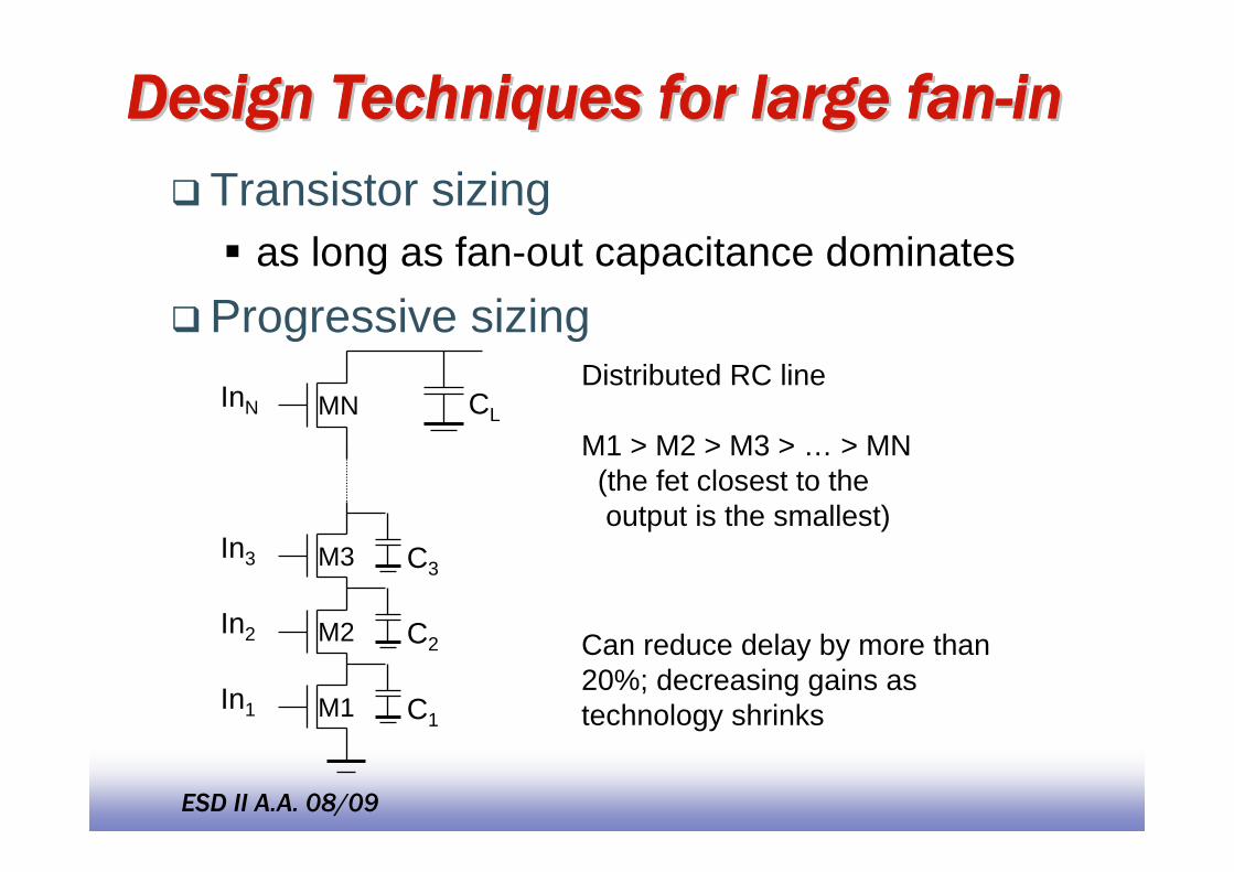
Design Techniques for large fanDesign Techniques for large fan--ininTransistor sizing
as long as fan-out capacitance dominatesProgressive sizingInN CL
C3
C2
C1In1
In2
In3
M1
M2
M3
MNDistributed RC line
M1 > M2 > M3 > … > MN(the fet closest to theoutput is the smallest)
Can reduce delay by more than 20%; decreasing gains as technology shrinks
EE14123
ESD II A.A. 08/09
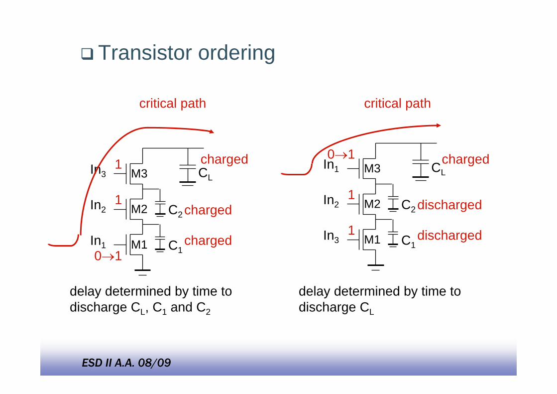
Transistor ordering
C2
C1In1
In2
In3
M1
M2
M3 CL
C2
C1In3
In2
In1
M1
M2
M3 CL
critical path critical path
charged1
0→1charged
charged1
delay determined by time to discharge CL, C1 and C2
delay determined by time to discharge CL
1
1
0→1 charged
discharged
discharged
EE14124
ESD II A.A. 08/09
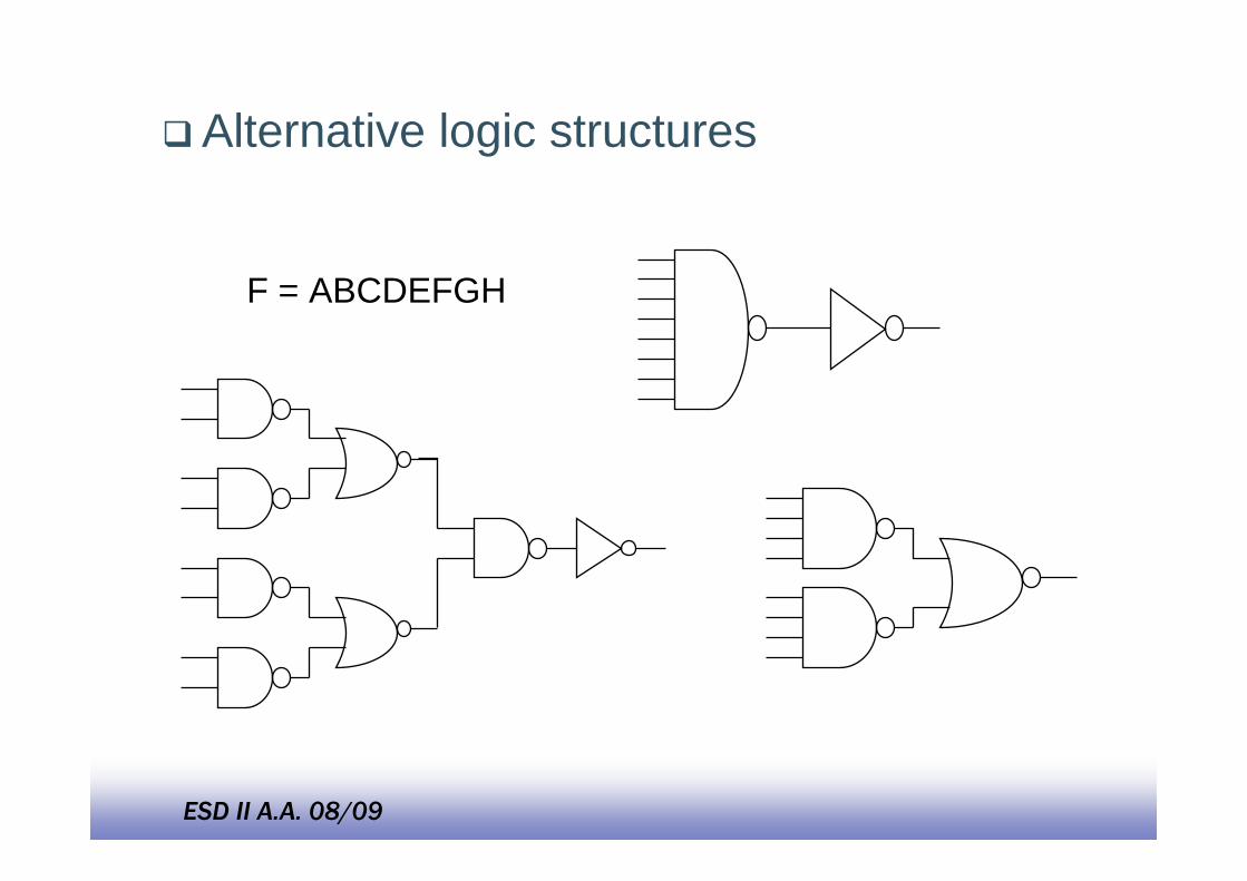
Alternative logic structures
F = ABCDEFGH
EE14125
ESD II A.A. 08/09
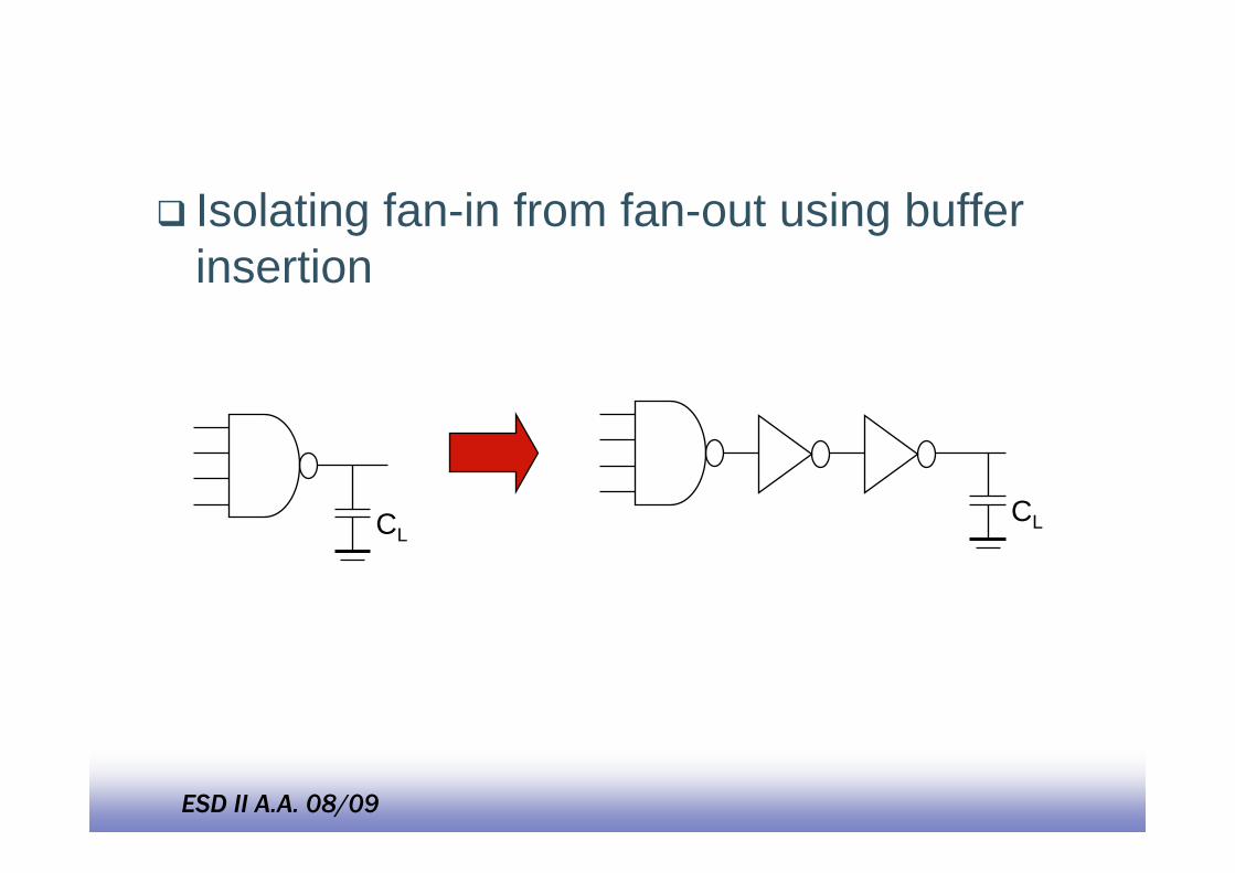
Isolating fan-in from fan-out using buffer insertion
CLCL
EE14126
ESD II A.A. 08/09
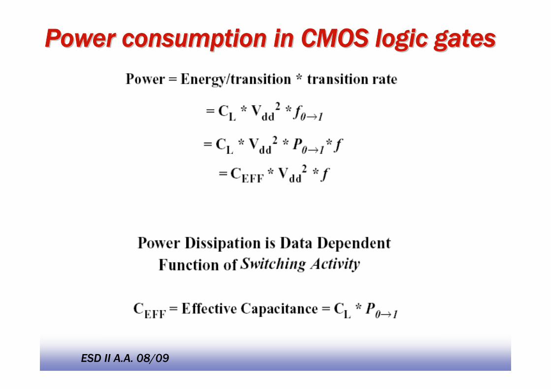
Power consumption in CMOS logic gatesPower consumption in CMOS logic gates
EE14127
ESD II A.A. 08/09
A
B
C
ZX
A
BZ
X
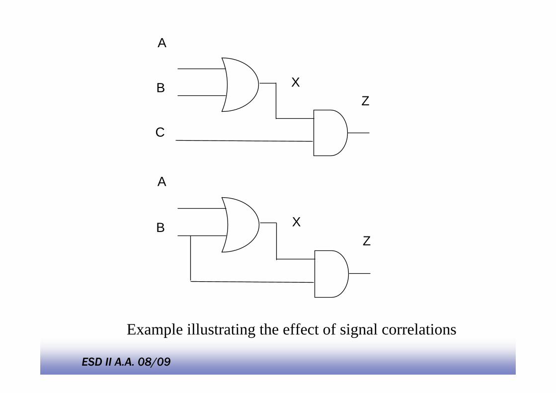
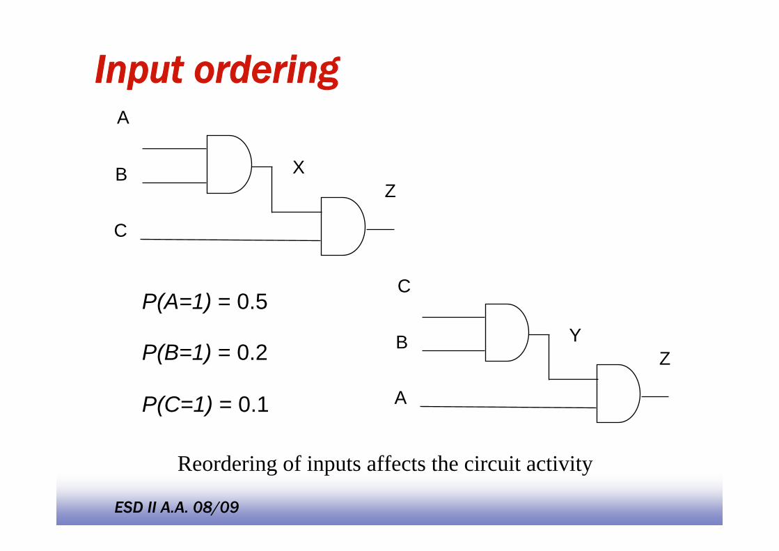
Example illustrating the effect of signal correlations
EE14128
ESD II A.A. 08/09
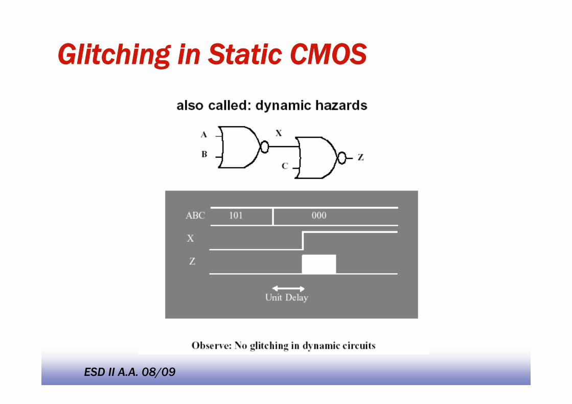
Glitching in Static CMOS
EE14129
ESD II A.A. 08/09
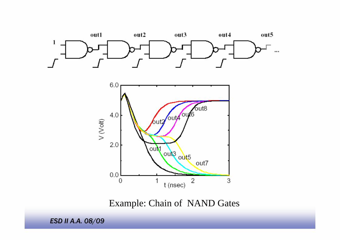
Example: Chain of NAND Gates
EE14130
ESD II A.A. 08/09
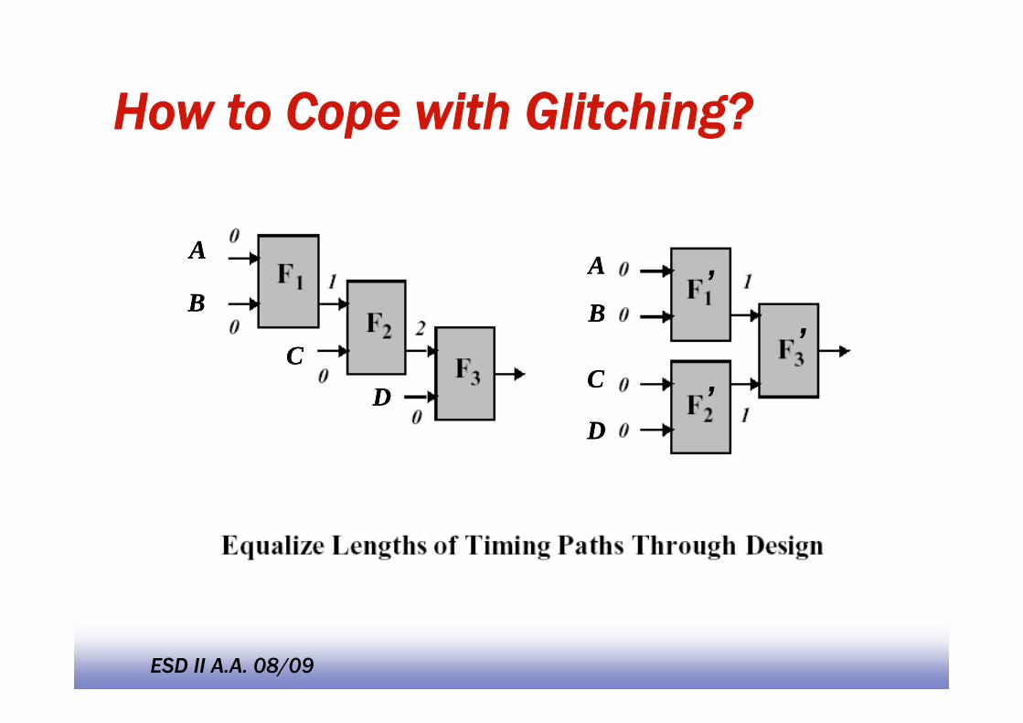
How to Cope with Glitching?
A
B
CD
A
B
C
D
,
,
,
A
B
CD
A
B
C
D
,
,
,
A
B
CD
A
B
C
D
,
,
,
EE14131
ESD II A.A. 08/09
Reordering of inputs affects the circuit activity
A
B
C
ZX
C
B
A
ZY
P(A=1) = 0.5
P(B=1) = 0.2
P(C=1) = 0.1
Input ordering
EE14132
ESD II A.A. 08/09
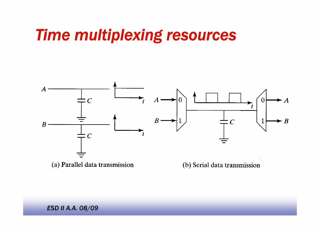
Time multiplexing resources
EE14133
ESD II A.A. 08/09
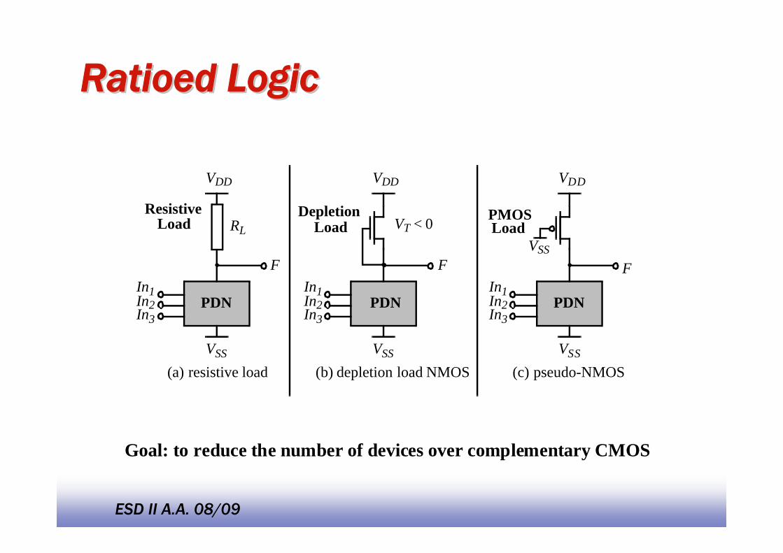
RatioedRatioed LogicLogic
VDD
VSS
PDNIn1In2In3
F
RLLoad
VDD
VSS
In1In2In3
F
VDD
VSS
PDNIn1In2In3
FVSS
PDN
Resistive DepletionLoad
PMOSLoad
(a) resistive load (b) depletion load NMOS (c) pseudo-NMOS
VT < 0
Goal: to reduce the number of devices over complementary CMOS
EE14134
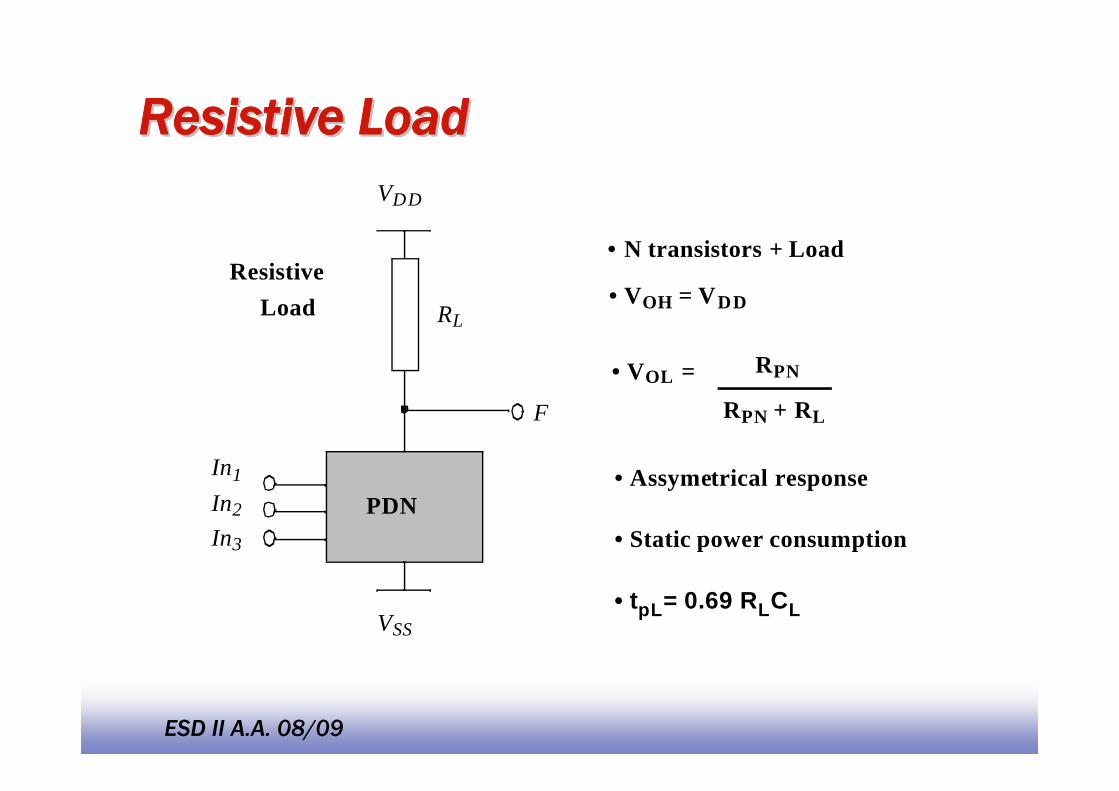
ESD II A.A. 08/09
VDD
VSS
PDNIn1In2In3
F
RLLoadResistive
N transistors + Load
• VOH = VDD
• VOL = RPN
RPN + RL
• Assymetrical response
• Static power consumption
•
• tpL= 0.69 RLCL
ResistiveResistive LoadLoad
EE14135
ESD II A.A. 08/09
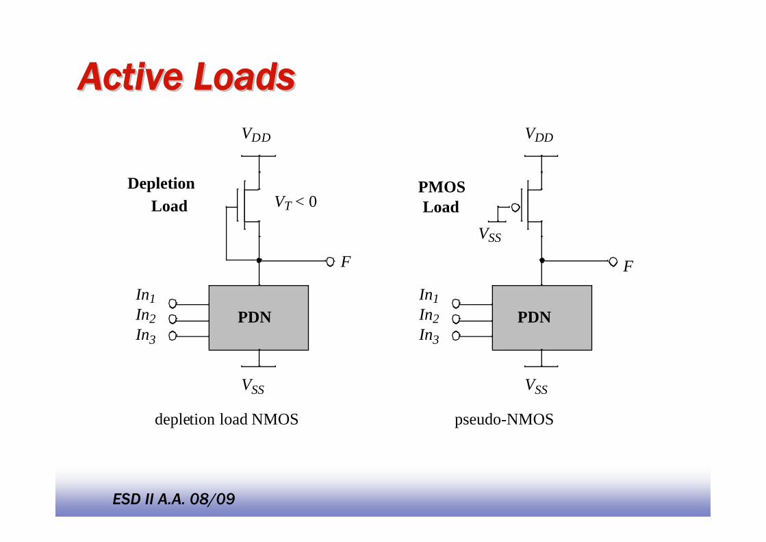
Active LoadsActive LoadsVDD
VSS
In1In2In3
F
VDD
VSS
PDNIn1In2In3
F
VSS
PDN
DepletionLoad
PMOSLoad
depletion load NMOS pseudo-NMOS
VT < 0
EE14136
ESD II A.A. 08/09
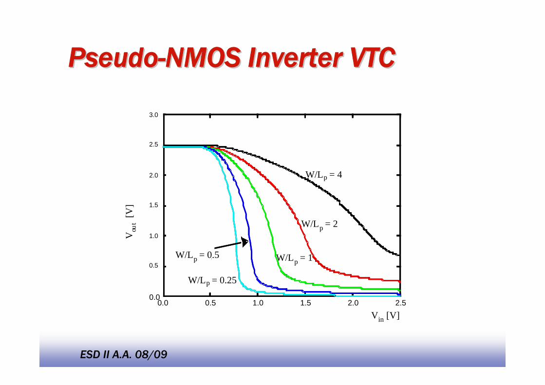
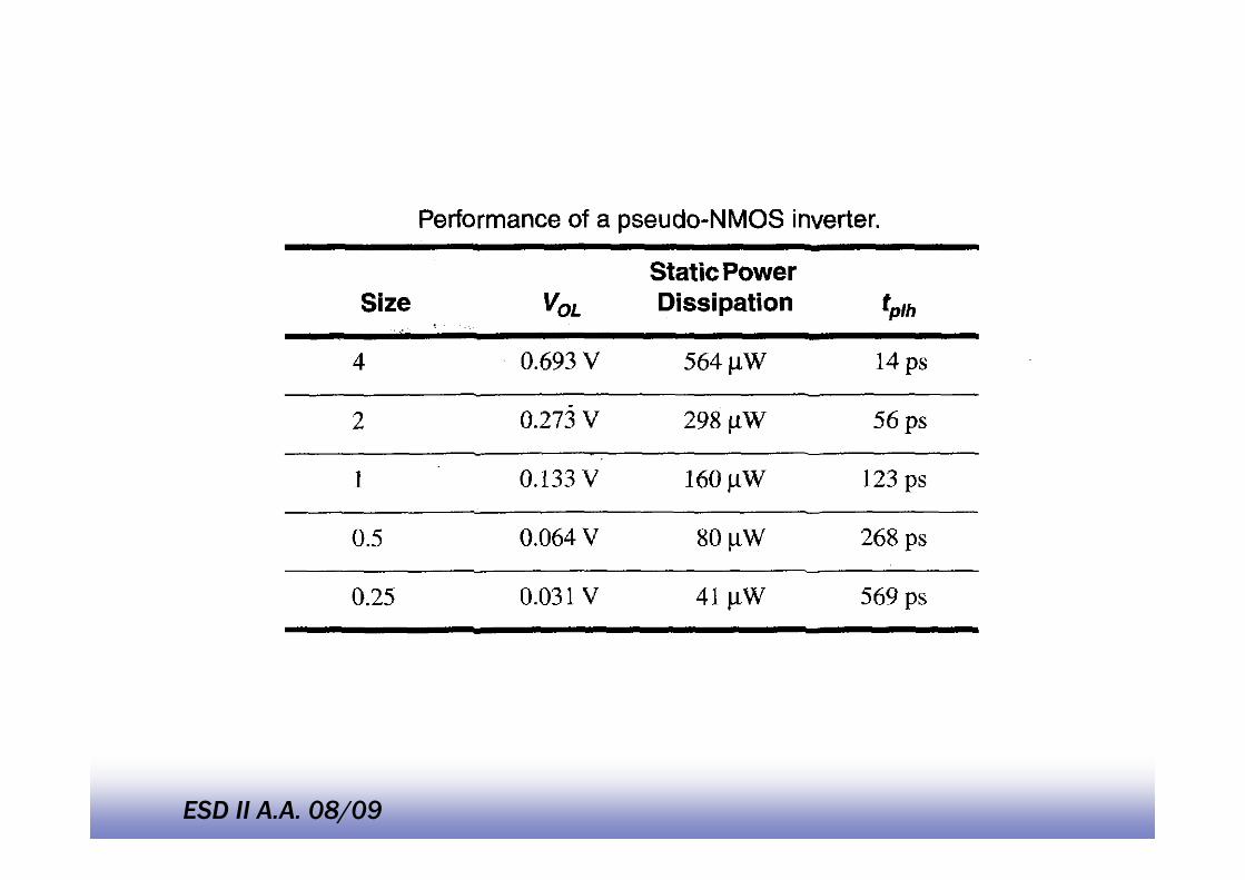
PseudoPseudo--NMOS Inverter VTCNMOS Inverter VTC
0.0 0.5 1.0 1.5 2.0 2.50.0
0.5
1.0
1.5
2.0
2.5
3.0
Vin [V]
Vou
t[V
]
W/Lp = 4
W/Lp = 2
W/Lp = 1
W/Lp = 0.25
W/Lp = 0.5
EE14137
ESD II A.A. 08/09
EE14138
ESD II A.A. 08/09
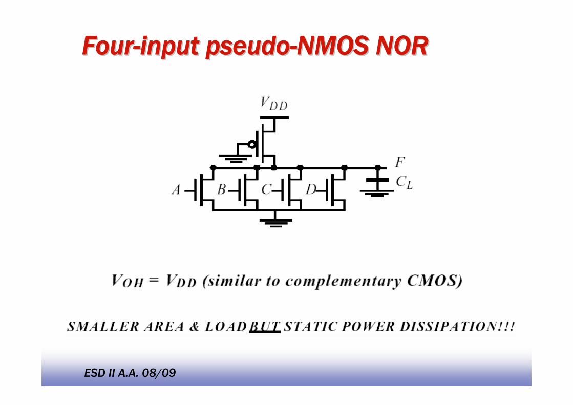
FourFour--input pseudoinput pseudo--NMOS NORNMOS NOR
EE14139
ESD II A.A. 08/09
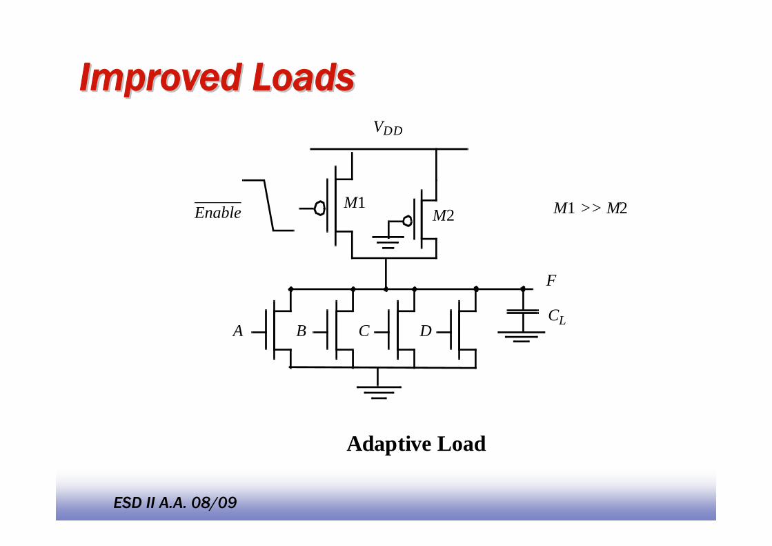
Improved LoadsImproved Loads
A B C D
F
CL
M1M2 M1 >> M2Enable
VDD
Adaptive Load
EE14140
ESD II A.A. 08/09
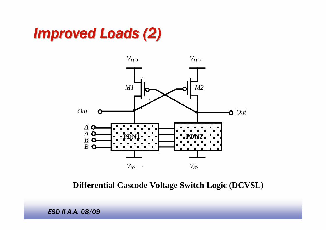
Improved Loads (2)Improved Loads (2)VDD
VSS
PDN1
Out
VDD
VSS
PDN2
Out
AABB
M1 M2
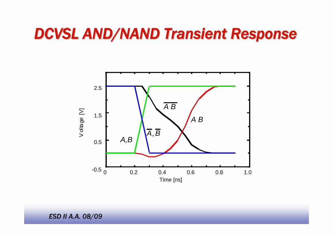
Differential Cascode Voltage Switch Logic (DCVSL)
EE14141
ESD II A.A. 08/09
0 0.2 0.4 0.6 0.8 1.0-0.5
0.5
1.5
2.5
Time [ns]
Vol
tage
[V] A B
A B
A,BA, B
DCVSL AND/NAND Transient ResponseDCVSL AND/NAND Transient Response
EE14142
ESD II A.A. 08/09
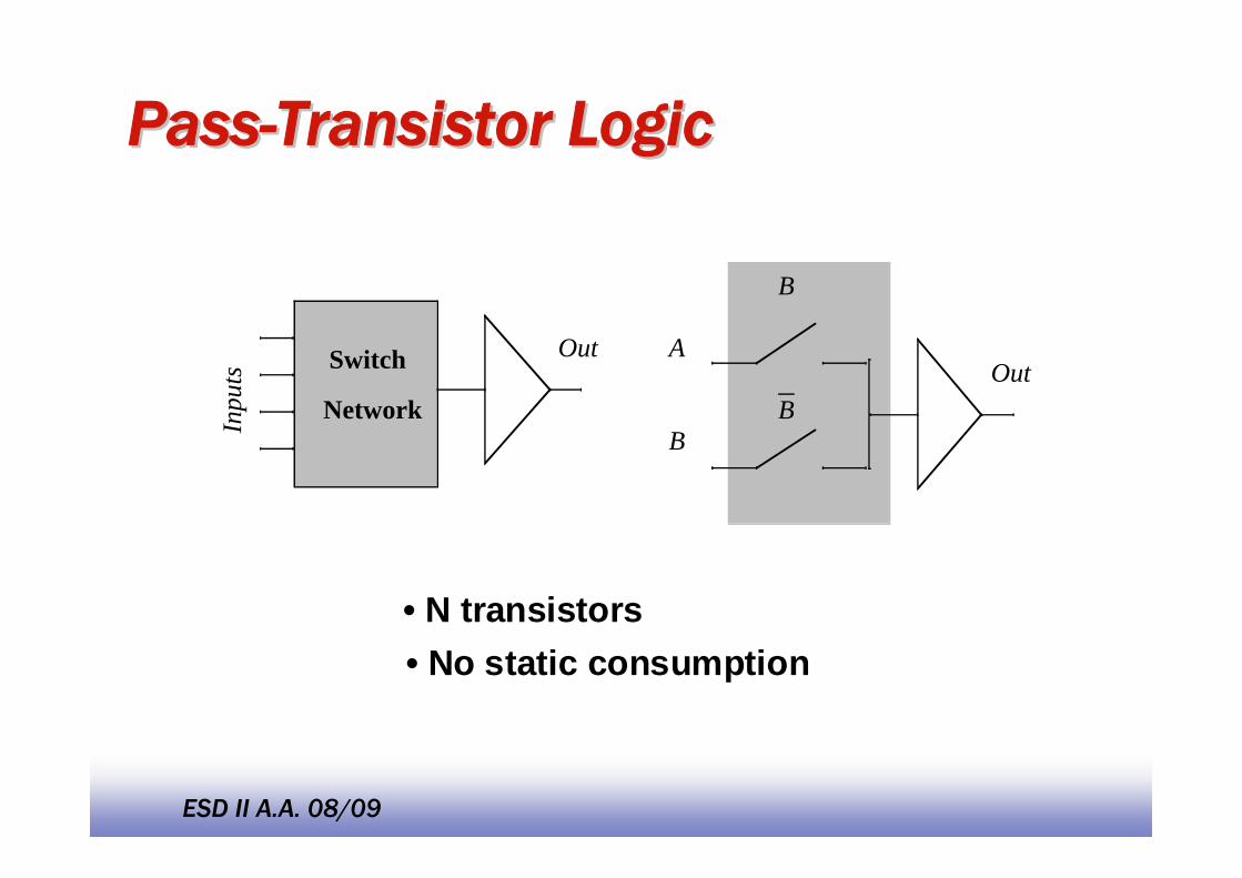
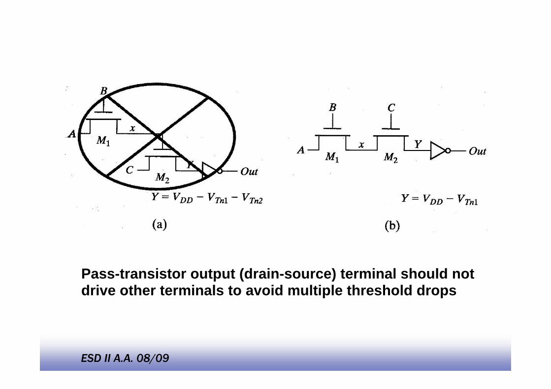
PassPass--Transistor LogicTransistor LogicIn
puts Switch
Network
OutOut
A
B
B
B
• N transistors• No static consumption
EE14143
ESD II A.A. 08/09
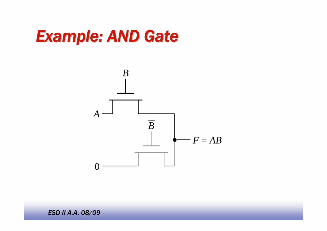
Example: AND GateExample: AND Gate
B
B
A
F = AB
0
EE14144
ESD II A.A. 08/09
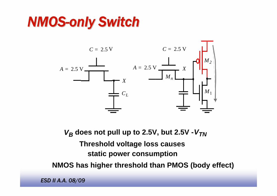
NMOSNMOS--only Switchonly Switch
A = 2.5 V
X
C = 2.5 V
CL
A = 2.5 V
C = 2.5 V
XM2
M1
Mn
Threshold voltage loss causesstatic power consumption
VB does not pull up to 2.5V, but 2.5V -VTN
NMOS has higher threshold than PMOS (body effect)
EE14145
ESD II A.A. 08/09
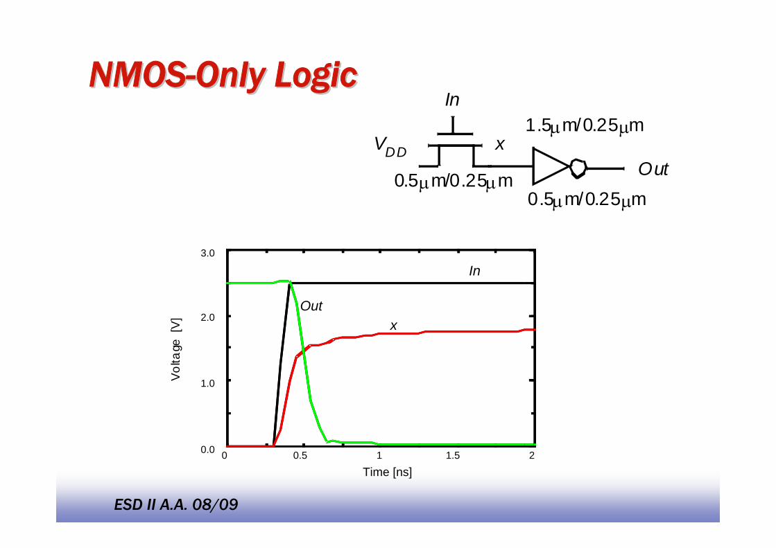
NMOSNMOS--Only LogicOnly Logic
VDD
In
Outx
0.5μm/0.25μm0.5μm/0.25μm
1.5μm/0.25μm
0 0.5 1 1.5 20.0
1.0
2.0
3.0
Time [ns]
Volta
ge[V
] xOut
In
EE14146
ESD II A.A. 08/09
Pass-transistor output (drain-source) terminal should not drive other terminals to avoid multiple threshold drops
EE14147
ESD II A.A. 08/09
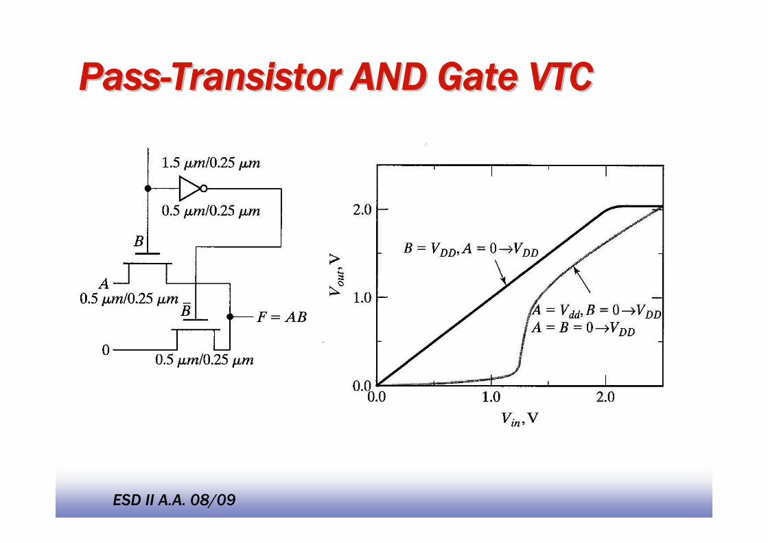
PassPass--Transistor AND Gate VTCTransistor AND Gate VTC
EE14148
ESD II A.A. 08/09
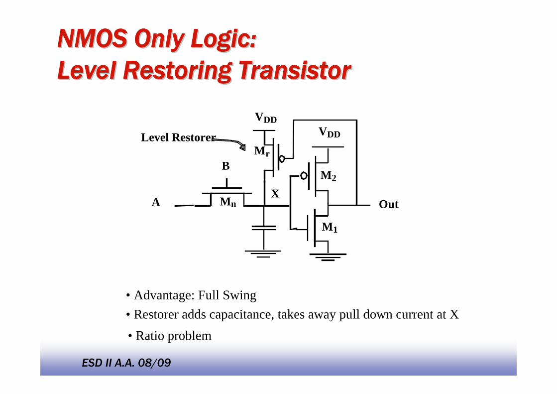
NMOS Only Logic: NMOS Only Logic: Level Restoring TransistorLevel Restoring Transistor
M2
M1
Mn
Mr
OutA
B
VDDVDDLevel Restorer
X
• Advantage: Full Swing• Restorer adds capacitance, takes away pull down current at X• Ratio problem
EE14149
ESD II A.A. 08/09
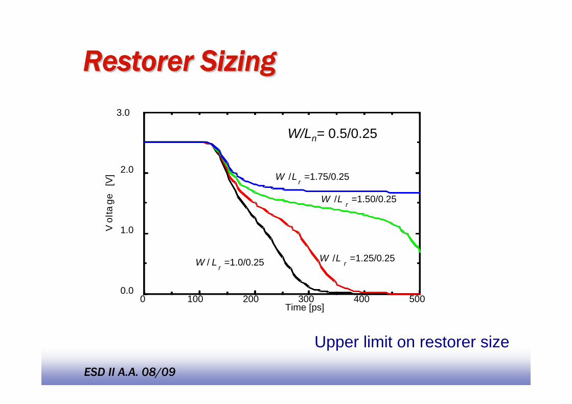
Restorer SizingRestorer Sizing
0 100 200 300 400 5000.0
1.0
2.0
W / Lr
=1.0/0.25 W /L r =1.25/0.25
W /Lr
=1.50/0.25
W /L r =1.75/0.25
Vo l
tag e
[V]
Time [ps]
3.0
W/Ln= 0.5/0.25
Upper limit on restorer size
EE14150
ESD II A.A. 08/09
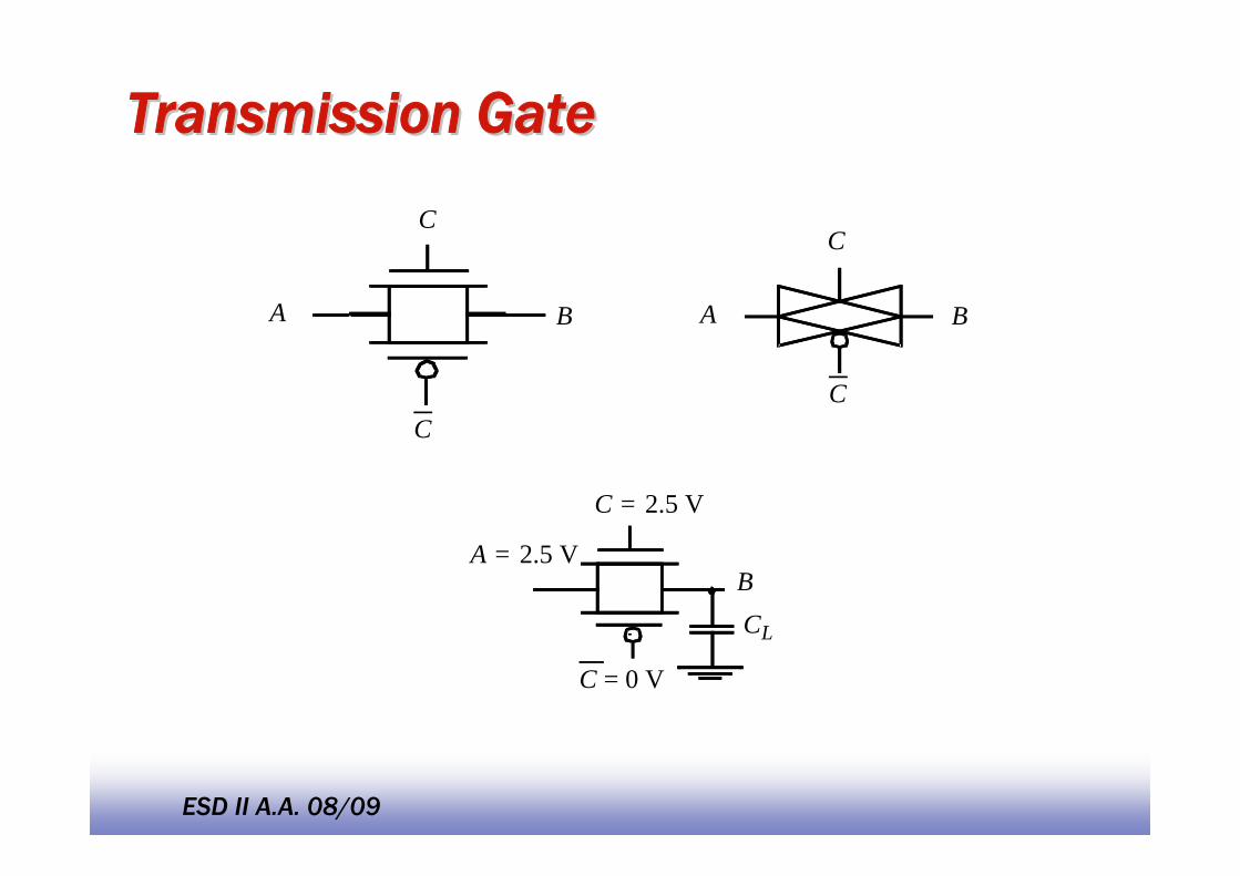
Transmission GateTransmission Gate
A B
C
C
A B
C
C
BCL
C = 0 V
A = 2.5 V
C = 2.5 V
EE14151
ESD II A.A. 08/09
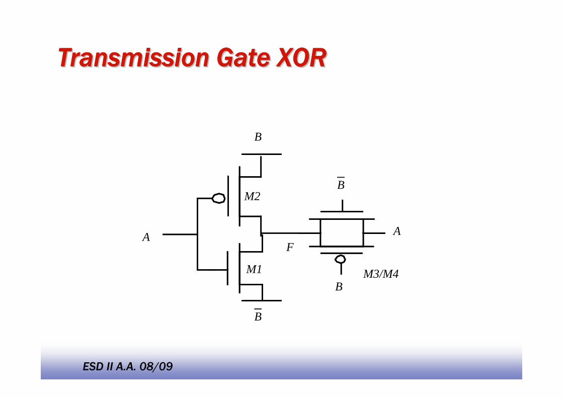
Transmission Gate XORTransmission Gate XOR
A
B
F
B
A
B
BM1
M2
M3/M4
EE14152
ESD II A.A. 08/09
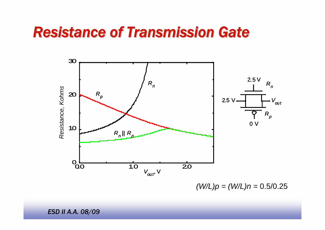
Resistance of Transmission GateResistance of Transmission Gate
Vout
0 V
2.5 V
2.5 VRn
Rp
0.0 1.0 2.00
10
20
30
Vout, V
Res
ista
nce,
ohm
s
Rn
Rp
Rn || RpRes
ista
nce,
Koh
ms
Vou t
0 V
2.5 V
2.5 VRn
Rp
0.0 1.0 2.00
10
20
30
Vout, V
Res
ista
nce,
ohm
s
Rn
Rp
Rn || Rp
Vout
0 V
2.5 V
2.5 VRn
Rp
0.0 1.0 2.00
10
20
30
Vout, V
Res
ista
nce,
ohm
s
Rn
Rp
Rn || RpRes
ista
nce,
Koh
ms
(W/L)p = (W/L)n = 0.5/0.25
EE14153
ESD II A.A. 08/09
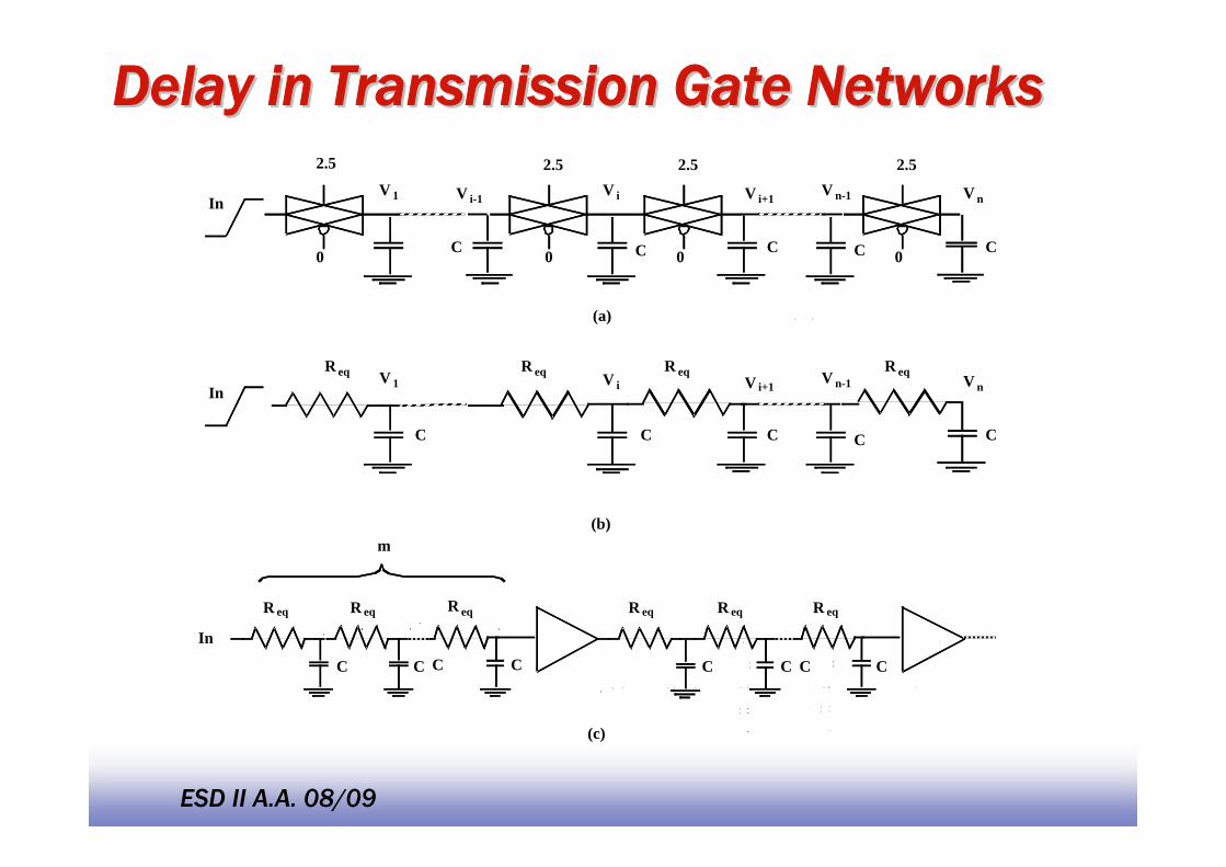
Delay in Transmission Gate NetworksDelay in Transmission Gate NetworksV 1 V i-1
C
2.5 2.5
0 0
V i V i+1
CC
2.5
0
V n-1 V n
CC
2.5
0
In
V 1 V i V i+1
C
V n-1 V n
CC
In
R eqR eq R eq R eq
CC
(a)
(b)
C
R eq R eq
C C
R eq
C C
R eq R eq
C C
R eq
C
In
m
(c)
EE14154
ESD II A.A. 08/09
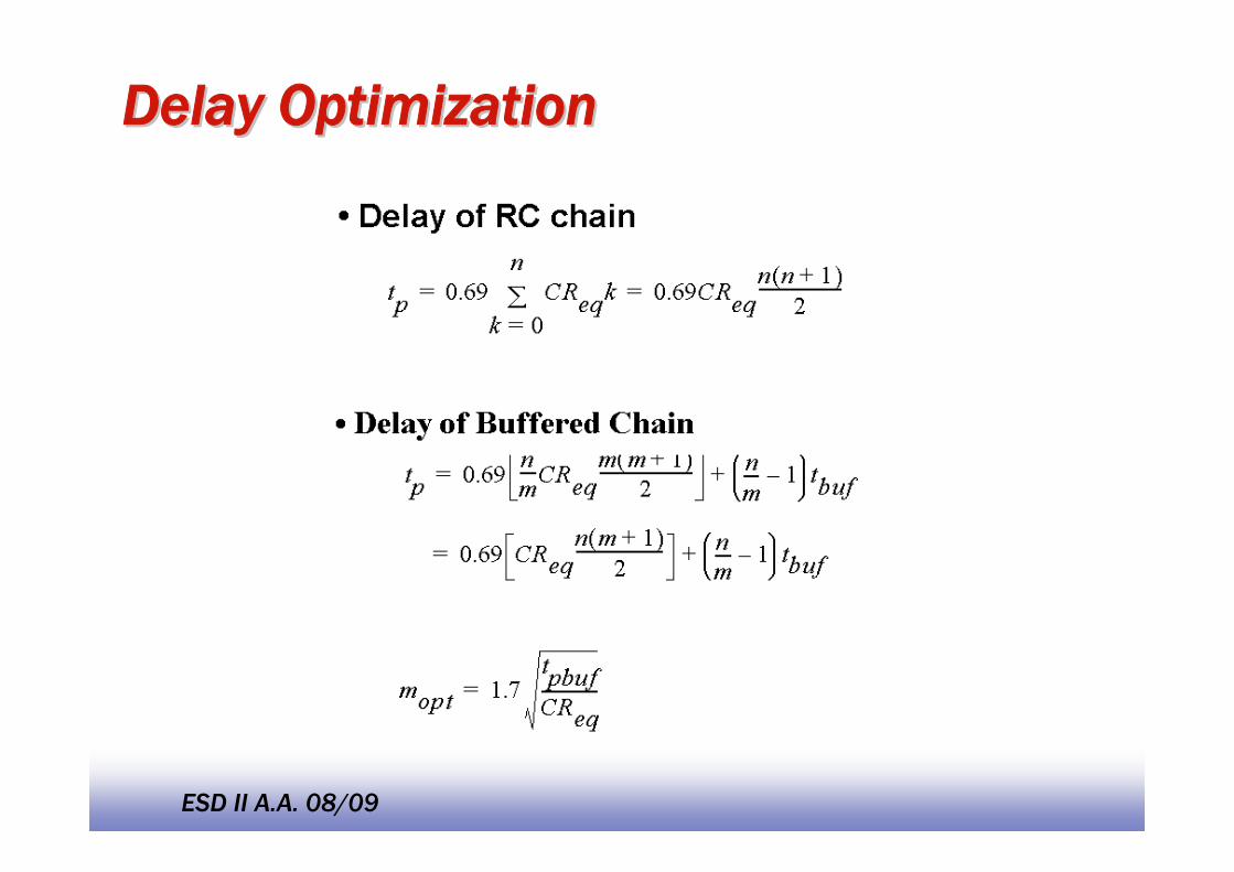
Delay OptimizationDelay Optimization