Embed Size (px)
Citation preview
Dual-band superconducting bandpass filterwith embedded resonator structure
Yong Heng, Xubo Guo, Bisong Cao, Zhijun Ying, Bin Wei,Xiaoping Zhang, Guoyong Zhang, Xiaoke Song andJingchen Wang
ELECT
A dual-band superconducting microstrip filter with two passbands of2.985–3.015 GHz and 3.045–3.075 GHz, respectively, is synthesisedby a frequency transformation method. Open-loop resonators withembedded single spiral resonators are proposed to realise the syn-thesised resonator frequencies and coupling coefficients. This structurehas the advantages of compact size and weak parasitic couplings,which benefit the implementation of the dual-band planar filter. Thefilter is successfully designed and fabricated on an MgO substrate.The measured results show high performance and match well withthe simulations.
Introduction: Modern multiband and multi-functional wireless systemsrequire efficient utilisation of the allocated frequency bands in anincreasingly crowded spectrum. Multiband filters are one of the keycomponents for wireless systems to satisfy such a requirement.Several different methods have been reported for designing multibandfilters [1–6]. One method is to connect several bandpass filters in parallelor cascade a broadband bandpass filter with a narrowband bandstop filterto obtain multiband characteristics [1]. This method is straightforward,but the circuit size is comparatively large. Multimode resonators, includ-ing stepped-impedance resonators and stub-loaded resonators, with theadvantage of compact size are widely used to design multiband filters[2, 3]. The disadvantage of this method is that the required guardbands between the multiple bandwidths should be relatively large.Moreover, it is difficult to adjust the couplings between the multimoderesonators to meet the requirements of multiple bandwidths simul-taneously. Synthesis methods including coupling matrix optimisationand frequency transformation are also used to design multiband filters[4–6]. However, it is a challenge to implement the synthesised topologywith planar structures because the problem of unwanted parasitic coup-lings is very complicated to solve, which leads to unsatisfactory returnloss.
In this Letter, a dual-band high-temperature superconducting (HTS)microstrip filter is proposed. The filter topology is synthesised by a fre-quency transformation method. Open-loop resonators with embeddedsingle spiral resonators are proposed to realise this topology. The pro-posed filter structure minimises the parasitic couplings between the res-onators and reduces the circuit size. The measured results show highperformance and match well with the simulations, which validates thedesign methods.
Filter design: The dual-band filter is synthesised by thelowpass-to-bandpass frequency transformation T introduced in [5]
V = T (v) = b1v
vo1− vo1
v
( )
− 1
b2 v/ vo2( )( )− vo2( )/v( )( )
where Ω is the normalised radian frequency, ω is the de-normalisedradian frequency and b1, b2, ωo1 and ωo2 are the parameters thatdefine the transformation. In our design, the dual-band filter is specifiedby two passbands with 2.985–3.015 GHz and 3.045–3.075 GHz,respectively. Then the transformation parameters can be calculated tobe [5]
[vo1, vo2] = 2p× [3.0295, 3.0301]
[b1, b2] = [50.49, 67.34]
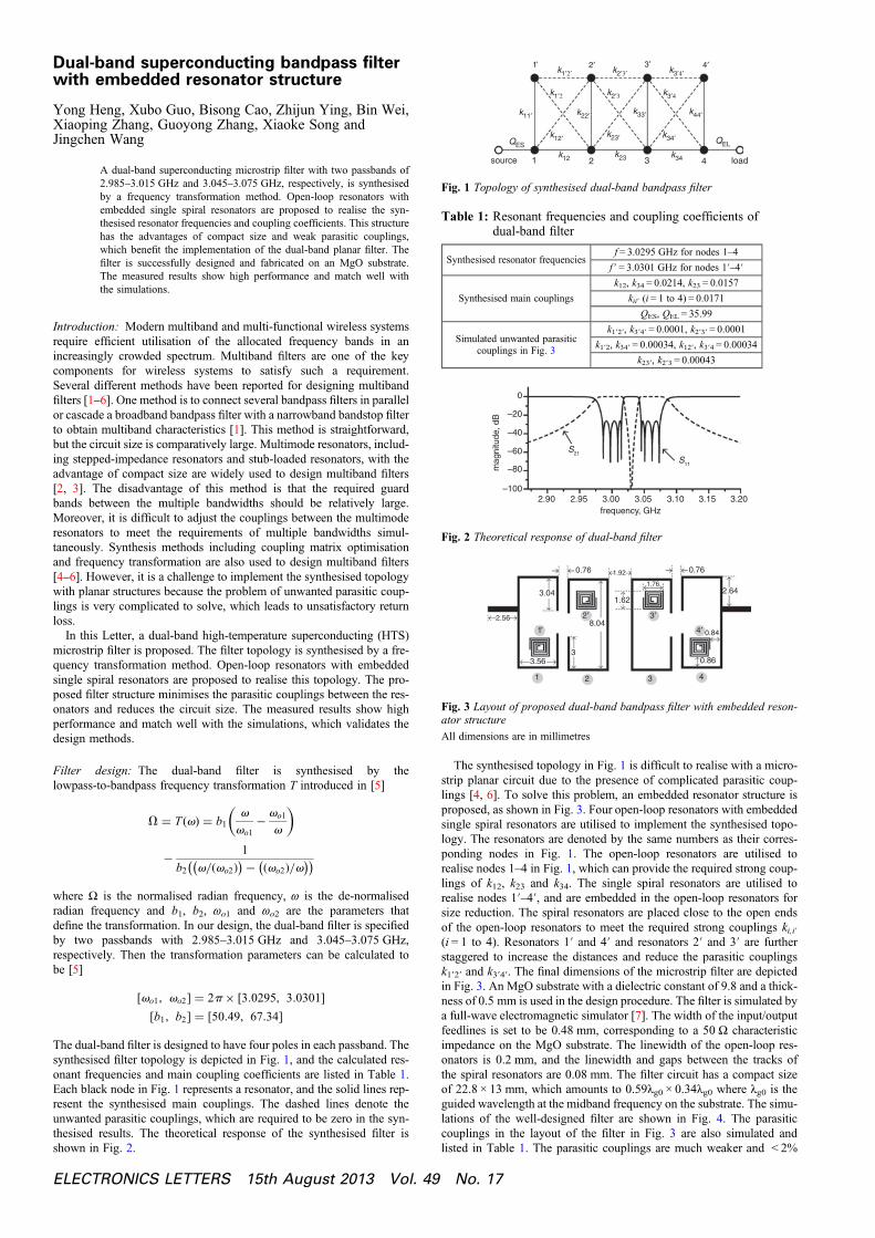
The dual-band filter is designed to have four poles in each passband. Thesynthesised filter topology is depicted in Fig. 1, and the calculated res-onant frequencies and main coupling coefficients are listed in Table 1.Each black node in Fig. 1 represents a resonator, and the solid lines rep-resent the synthesised main couplings. The dashed lines denote theunwanted parasitic couplings, which are required to be zero in the syn-thesised results. The theoretical response of the synthesised filter isshown in Fig. 2.
RONICS LETTERS 15th August 2013 Vol. 49
k12
k12¢ k23¢ k34¢
k44¢
k3¢4
k1¢2¢
k11¢
k2¢3¢ k3¢4¢
k2¢3k1¢2
k33¢k22¢
QESQEL
source 1 2 3 4 loadk23 k34
1¢ 2¢ 3¢ 4¢
Fig. 1 Topology of synthesised dual-band bandpass filter
Table 1: Resonant frequencies and coupling coefficients ofdual-band filter
Synthesised resonator frequencies
No. 17
f = 3.0295 GHz for nodes 1–4f ′ = 3.0301 GHz for nodes 1′–4′
Synthesised main couplings
k12, k34 = 0.0214, k23 = 0.0157
kii′ (i = 1 to 4) = 0.0171
QES, QEL = 35.99
Simulated unwanted parasiticcouplings in Fig. 3
k1′2′, k3′4′ = 0.0001, k2′3′ = 0.0001
k1′2, k34′ = 0.00034, k12′, k3′4 = 0.00034
k23′, k2′3 = 0.00043
frequency, GHz2.90 2.95 3.00 3.05 3.10 3.15 3.20
mag
nitu
de, d
B
0
–20
–40
–60
–80
–100
S11
S21
Fig. 2 Theoretical response of dual-band filter
0.76 1.92
3.04
2.56
1¢
2¢ 3¢
4¢8.04
0.84
0.863
1 2 3 4
3.56
1.62
1.76
0.76
2.64
Fig. 3 Layout of proposed dual-band bandpass filter with embedded reson-ator structure
All dimensions are in millimetres
The synthesised topology in Fig. 1 is difficult to realise with a micro-strip planar circuit due to the presence of complicated parasitic coup-lings [4, 6]. To solve this problem, an embedded resonator structure isproposed, as shown in Fig. 3. Four open-loop resonators with embeddedsingle spiral resonators are utilised to implement the synthesised topo-logy. The resonators are denoted by the same numbers as their corres-ponding nodes in Fig. 1. The open-loop resonators are utilised torealise nodes 1–4 in Fig. 1, which can provide the required strong coup-lings of k12, k23 and k34. The single spiral resonators are utilised torealise nodes 1′–4′, and are embedded in the open-loop resonators forsize reduction. The spiral resonators are placed close to the open endsof the open-loop resonators to meet the required strong couplings ki,i′(i = 1 to 4). Resonators 1′ and 4′ and resonators 2′ and 3′ are furtherstaggered to increase the distances and reduce the parasitic couplingsk1′2′ and k3′4′. The final dimensions of the microstrip filter are depictedin Fig. 3. An MgO substrate with a dielectric constant of 9.8 and a thick-ness of 0.5 mm is used in the design procedure. The filter is simulated bya full-wave electromagnetic simulator [7]. The width of the input/outputfeedlines is set to be 0.48 mm, corresponding to a 50 Ω characteristicimpedance on the MgO substrate. The linewidth of the open-loop res-onators is 0.2 mm, and the linewidth and gaps between the tracks ofthe spiral resonators are 0.08 mm. The filter circuit has a compact sizeof 22.8 × 13 mm, which amounts to 0.59λg0 × 0.34λg0 where λg0 is theguided wavelength at the midband frequency on the substrate. The simu-lations of the well-designed filter are shown in Fig. 4. The parasiticcouplings in the layout of the filter in Fig. 3 are also simulated andlisted in Table 1. The parasitic couplings are much weaker and < 2%
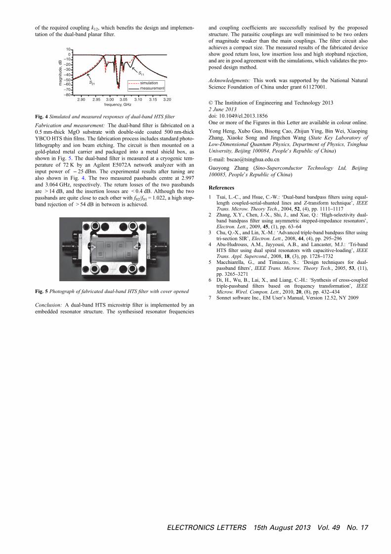
of the required coupling k12, which benefits the design and implemen-tation of the dual-band planar filter.
100
–10–20–30–40–50–60–70–80
mag
nitu
de, d
B
frequency, GHz
simulationS21
S11
measurement
2.90 2.95 3.00 3.05 3.10 3.15 3.20
Fig. 4 Simulated and measured responses of dual-band HTS filter
Fabrication and measurement: The dual-band filter is fabricated on a0.5 mm-thick MgO substrate with double-side coated 500 nm-thickYBCO HTS thin films. The fabrication process includes standard photo-lithography and ion beam etching. The circuit is then mounted on agold-plated metal carrier and packaged into a metal shield box, asshown in Fig. 5. The dual-band filter is measured at a cryogenic tem-perature of 72 K by an Agilent E5072A network analyzer with aninput power of − 25 dBm. The experimental results after tuning arealso shown in Fig. 4. The two measured passbands centre at 2.997and 3.064 GHz, respectively. The return losses of the two passbandsare > 14 dB, and the insertion losses are < 0.4 dB. Although the twopassbands are quite close to each other with f02/f01 = 1.022, a high stop-band rejection of > 54 dB in between is achieved.
Fig. 5 Photograph of fabricated dual-band HTS filter with cover opened
Conclusion: A dual-band HTS microstrip filter is implemented by anembedded resonator structure. The synthesised resonator frequencies
ELECTRONIC
and coupling coefficients are successfully realised by the proposedstructure. The parasitic couplings are well minimised to be two ordersof magnitude weaker than the main couplings. The filter circuit alsoachieves a compact size. The measured results of the fabricated deviceshow good return loss, low insertion loss and high stopband rejection,and are in good agreement with the simulations, which validates the pro-posed design method.
Acknowledgments: This work was supported by the National NaturalScience Foundation of China under grant 61127001.
© The Institution of Engineering and Technology 20132 June 2013doi: 10.1049/el.2013.1856One or more of the Figures in this Letter are available in colour online.
Yong Heng, Xubo Guo, Bisong Cao, Zhijun Ying, Bin Wei, XiaopingZhang, Xiaoke Song and Jingchen Wang (State Key Laboratory ofLow-Dimensional Quantum Physics, Department of Physics, TsinghuaUniversity, Beijing 100084, People’s Republic of China)E-mail: [email protected]
Guoyong Zhang (Sino-Superconductor Technology Ltd, Beijing100085, People’s Republic of China)
References
1 Tsai, L.-C., and Hsue, C.-W.: ‘Dual-band bandpass filters using equal-length coupled-serial-shunted lines and Z-transform technique’, IEEETrans. Microw. Theory Tech., 2004, 52, (4), pp. 1111–1117
2 Zhang, X.Y., Chen, J.-X., Shi, J., and Xue, Q.: ‘High-selectivity dual-band bandpass filter using asymmetric stepped-impedance resonators’,Electron. Lett., 2009, 45, (1), pp. 63–64
3 Chu, Q.-X., and Lin, X.-M.: ‘Advanced triple-band bandpass filter usingtri-section SIR’, Electron. Lett., 2008, 44, (4), pp. 295–296
4 Abu-Hudrouss, A.M., Jayyousi, A.B., and Lancaster, M.J.: ‘Tri-bandHTS filter using dual spiral resonators with capacitive-loading’, IEEETrans. Appl. Supercond., 2008, 18, (3), pp. 1728–1732
5 Macchiarella, G., and Timiazzo, S.: ‘Design techniques for dual-passband filters’, IEEE Trans. Microw. Theory Tech., 2005, 53, (11),pp. 3265–3271
6 Di, H., Wu, B., Lai, X., and Liang, C.-H.: ‘Synthesis of cross-coupledtriple-passband filters based on frequency transformation’, IEEEMicrow. Wirel. Compon. Lett., 2010, 20, (8), pp. 432–434
7 Sonnet software Inc., EM User’s Manual, Version 12.52, NY 2009
S LETTERS 15th August 2013 Vol. 49 No. 17