Embed Size (px)
Citation preview

Jeong et al. Nanoscale Research Letters 2014, 9:619http://www.nanoscalereslett.com/content/9/1/619
NANO EXPRESS Open Access
Dual active layer a-IGZO TFT via homogeneousconductive layer formation by photochemicalH-dopingSeung-Ki Jeong1, Myeong-Ho Kim1, Sang-Yeon Lee2, Hyungtak Seo2* and Duck-Kyun Choi1*
Abstract
In this study, InGaZnO (IGZO) thin film transistors (TFTs) with a dual active layer (DAL) structure are fabricated byinserting a homogeneous embedded conductive layer (HECL) in an amorphous IGZO (a-IGZO) channel with theaim of enhancing the electrical characteristics of conventional bottom-gate-structure TFTs. A highly conductiveHECL (carrier concentration at 1.6 × 1013 cm−2, resistivity at 4.6 × 10⁻³ Ω∙cm, and Hall mobility at 14.6 cm2/Vs atroom temperature) is fabricated using photochemical H-doping by irradiating UV light on an a-IGZO film. Theelectrical properties of the fabricated DAL TFTs are evaluated by varying the HECL length. The results reveal thatcarrier mobility increased proportionally with the HECL length. Further, a DAL TFT with a 60-μm-long HECLembedded in an 80-μm-long channel exhibits comprehensive and outstanding improvements in its electricalproperties: a saturation mobility of 60.2 cm2/Vs, threshold voltage of 2.7 V, and subthreshold slope of 0.25 V/decadeagainst the initial values of 19.9 cm2/Vs, 4.7 V, and 0.45 V/decade, respectively, for a TFT without HECL. This resultconfirms that the photochemically H-doped HECL significantly improves the electrical properties of DAL IGZO TFTs.
Keywords: TFT; UV irradiation; Photochemical doping; Hydrogen donor; a-IGZO; Dual active layers
BackgroundRecently, there has been a growing need in the next-generation display industry for the development of newchannel thin film transistors (TFTs) in order to implementactive-matrix organic light-emitting diode (AMOLED)displays with a large area, rapid information transmission,high resolution, and high frame rates [1]. Among the vari-ous candidates for new channel TFTs, oxide TFTs are re-ceiving great attention owing to their several advantagessuch as high electron mobility, high on/off ratio, low leak-age current, and good uniformity even when deposited atlow temperatures. In particular, amorphous InGaZnO(a-IGZO) TFT is emerging as the most viable option amongoxide TFTs for use in the next-generation display industry,as it provides good uniformity as an amorphous TFT suit-able for large displays and has a relatively high mobility ofover 10 cm2/Vs [2-4].
* Correspondence: [email protected]; [email protected] of Materials Science and Engineering and Department ofEnergy System Research, Ajou University, 206 Worldcup-ro, Yeongtong-Gu,Suwon 443-739, Republic of Korea1Department of Materials Science and Engineering, 222 Wangsimni-Ro,Seongdong-Gu, Hanyang University, Seoul 133-791, Republic of Korea
© 2014 Jeong et al.; licensee Springer. This is aAttribution License (http://creativecommons.orin any medium, provided the original work is p
A-IGZO TFT has higher electron mobility than exist-ing silicon-based TFTs, which are less amorphous. How-ever, for OLED pixels that are utilized in large AMOLEDTVs, high current is generally required in order to emitlight through electrical current injection. In addition,there is a great demand for TFTs with electron mobilityhigher than 30 cm2/Vs in order to realize the requireddisplay resolutions and pixel circuits [5]. To fulfill theserequirements, extensive research has been conducted inan attempt to enhance the electron mobility of a-IGZOvia different methods, including oxygen vacancy control,[6,7] hydrogen annealing, [8,9] use of a Ca capping layer,[10] sputtering power control, [6] and by combining vari-ous oxide components [11,12]. However, oxygen vacancycontrol - one of the most commonly used methods to en-hance the electrical conductivity of oxide semiconductors -may improve their conductivity, but the conductivityrange in which this method is applicable is very limited.Hydrogen annealing increases the number of oxygen va-cancies by artificially creating a reducing atmosphere andmakes it possible to realize high electrical conductivity;however, this method requires a lengthy thermal process
n Open Access article distributed under the terms of the Creative Commonsg/licenses/by/4.0), which permits unrestricted use, distribution, and reproductionroperly credited.

Jeong et al. Nanoscale Research Letters 2014, 9:619 Page 2 of 9http://www.nanoscalereslett.com/content/9/1/619
carried out above 300°C and is very limited in its applic-ability as it may damage surrounding devices throughrapid hydrogen diffusion. In addition, attempts have beenmade to enhance the electron mobility of a-IGZO byforming an additional Ca capping layer on top of the ac-tive layer to induce the reduction of a-IGZO and increasethe number of oxygen vacancies. However, this methodencountered problems such as restrictions by the sur-rounding environment due to vulnerability of Ca to oxy-gen or moisture in the atmosphere and the complexityof the fabrication process in forming additional layers[10]. Further, sputtering power control and the combin-ation of various oxide materials have reproducibility prob-lems, since target, equipment, and process requirementshave not been standardized.With this background, many researches have been con-
ducted on dual active layer (DAL) TFTs to enhance theirmobility by forming additional materials with high elec-trical conductivity on either the top or bottom of activelayers. Kim et al. [13] achieved improvement in mobilityby depositing an additional layer of a Mo thin film on theactive layer. However, the mobility did not increasenoticeably (2.5 to 4.7 cm2/Vs), and the transparencydecreased with increasing metal length. In another study,a high electrical conductivity oxide such as ITO was em-bedded in the channel path of the active layer to enhanceboth transmittance and mobility [14]. However, in thismethod, an interface is generated between the activelayer and oxide material owing to the formation of a het-erojunction [15], and this interface formation may de-grade the electrical properties of the TFTs.Hence, clearly distinguished from all the above-
discussed previous reports, the present study was focusedon high-performance DAL TFTs fabricated using a strik-ingly convenient optical method called ‘permanent photo-chemical doping,’ which can uniformly enhance electricalproperties by the effective H donor incorporation in thechannel, in an attempt to resolve the issues encounteredby existing DAL TFTs. Among the available oxide semi-conductors, a-IGZO with excellent electrical propertieswas used for fabricating the TFT active layer, and a homo-geneous embedded conductive layer (HECL) obtainedthrough photochemical doping at room temperature wasembedded in the channel path to enhance electrical mo-bility. In addition, the electrical characteristics of the fabri-cated DAL TFTs were evaluated by varying the HECLlength within a certain range to be shorter than the lengthof the active layer to investigate the effect of HECL on thechannel path.
MethodsBottom-gate-structure TFTs with an embedded highlyconductive a-IGZO path in a-IGZO active layer werefabricated on a glass substrate. A 100-nm-thick Mo gate
electrode was deposited using DC sputtering at roomtemperature and patterned out using wet etching. Thiswas followed by the deposition of a 100-nm-thick SiO2
gate insulator at 300°C using plasma-enhanced chemicalvapor deposition. For HECL formation, a 20-nm-thicka-IGZO layer was deposited on PR-patterned SiO2 sub-strates with a width of 50 μm and lengths of 20, 40, and60 μm by RF sputtering at room temperature by using asingle oxide target. During a-IGZO deposition, an ambi-ent atmosphere of Ar:O2 with a ratio of 90:10 was main-tained at 5 mTorr. For HECL formation, after a lift-offprocess, patterned a-IGZO layers were steadily irradiatedby deep-UV light (with main wavelengths of 185 and 254nm) for 240 min. An additional 20-nm-thick active layerof a-IGZO was then deposited at an RF power of 40 Wand room temperature. The 50-μm-wide and 80-μm-longa-IGZO active layer was patterned again using a lift-offprocess. For fabricating source and drain electrodes, 100-nm-thick Mo layers were deposited using DC sputteringat room temperature.The electrical properties of the fabricated TFTs were
evaluated via current–voltage (I-V) measurements per-formed using an Agilent E5270B parameter analyzer(Agilent Technologies, Inc., Santa Clara, CA, USA). Theelectrical properties of the HECL itself were analyzedusing the Van der Pauw method by Hall measurement(Ecopia HMS 3000, Ecopia, Anyang, Korea) at roomtemperature. The chemical compositions of the oxidethin films were analyzed using X-ray photoelectron spec-troscopy (XPS; Theta probe base system, Thermo FisherScientific Co., Seoul, South Korea). The energy reso-lution for each point was 0.05 eV, and the peak energywas self-calibrated to C1s and O1s reference peak states.The optical absorption data were measured by a rotatingcompensator-enhanced SE device with a spectral reso-lution of 15 meV and were analyzed using a three-phaseoptical model.
Results and discussionWe fabricated DAL TFTs by utilizing the bottom-gate-structure TFT that is typically used in displays becauseof its superior surface properties and also because itdoes not require a separate shield layer. Figure 1 showsa schematic of the fabrication process for a DAL TFTwith a channel width and length of 50 and 80 μm, re-spectively. The DALs were fabricated by forming anHECL below the active layer; the placement of theHECL was selected by considering the actual channelpath formed between the source and drain. When usinga DAL structure design in which the DAL is formed byemploying other highly conductive materials, the elec-tronic band structure of these materials should be con-sidered. This is because injected carriers from the sourceelectrode can be blocked by the formation of a barrier

Figure 1 A schematic representation of the fabrication process for DAL TFTs in the process order from (a-e). The placement of the20-nm-thick HECL was selected by considering the channel path formed between the actual source and drain. To confirm the direct influence ofHECL, the HECL length was varied within a range to be shorter than the channel path (0, 20, 40, and 60 μm).
Jeong et al. Nanoscale Research Letters 2014, 9:619 Page 3 of 9http://www.nanoscalereslett.com/content/9/1/619
and their movement toward the drain electrode can behindered, which will lead to low mobility [14]. However,under such a situation of barrier formation, the electricalproperties are expected not to degrade, since the photo-chemically processed highly conductive HECL and theactive layer are formed from the same material, namely,a-IGZO, and thus, they form a pseudo-homogeneousjunction.Figure 2 shows the I-V curves, Hall mobility, and car-
rier concentration for a-IGZO thin films, depicting thedependence of their electrical properties on UV irradi-ation time in an air atmosphere; the films were depositedon a glass substrate at an Ar:O2 partial pressure ratio of90:10 at room temperature. By comparing the electricalproperties of a-IGZO thin films at various UV irradiation
-10 -5 0 5 10 15 2010
-14
10-13
10-12
10-11
10-10
10 -9
10 -8
10 -7
10 -6
10 -5
10 -4
10-3
10-2
0min
30min
1hr
2hr
Cu
rren
t(A
)
Voltage(V)
UV4hr
a b
Hal
l mo
bili
ty (
cm2 /V
sec)
Figure 2 Electrical properties such as conductivity and Hall mobility asuch as (a) conductivity and (b) Hall mobility and carrier concentration ofand 240 min). As UV irradiation time increases, electrical properties increase
times, we confirmed that the electrical conductivityincreased up to nine orders of magnitude proportionallyto UV irradiation time, although the initial electricalproperties of the thin films were identical. According toHall measurement result at the room temperature onUV-irradiated a-IGZO film, it was confirmed that elec-trical properties such as Hall mobility and carrier con-centration of the a-IGZO film also increase as UVirradiation time increases. In particular, the Hall meas-urement on 4-h UV-irradiated a-IGZO film revealed itsmetallic electrical properties such as the carrier concen-tration at 1.6 × 1013 cm−2, resistivity at 4.6 × 10⁻³ Ω∙cm,and Hall mobility at 14.6 cm2/Vs at room temperature.Since the Hall measurement was impossible for the as-deposited a-IGZO due to its highly insulating property,
0 30 60 90 120 150 180 210 24023456789
10111213141516
1016
1017
1018
1019
1020
Car
rier
co
nce
ntr
atio
n (
cm-3)
UV irradiation time (min)
nd carrier concentration of a-IGZO thin films. Electrical propertiesa-IGZO thin films as a function of UV irradiation time (0, 30, 60, 120,linearly owing to permanent optical doping.

Jeong et al. Nanoscale Research Letters 2014, 9:619 Page 4 of 9http://www.nanoscalereslett.com/content/9/1/619
this is equivalent to the insulator-to-metal conversion ofamorphous oxide by UV irradiation. This UV irradiationeffect is permanently maintained since the time-dependant Hall measurement revealed no significantchange in electrical properties over a 4-week air-agingtest [see Additional file 1: Figure S1 for air-aging time-dependant Hall measurement data], and this impliesthat UV irradiation on a-IGZO more possibly leads toan irreversible change in chemistry acting as chemicaldoping to alter the electrical property of a-IGZO signifi-cantly. Therefore, the in-depth investigation on surfacechemistry upon UV irradiation was performed by XPSanalysis in the next section.XPS analyses were performed to investigate the origin
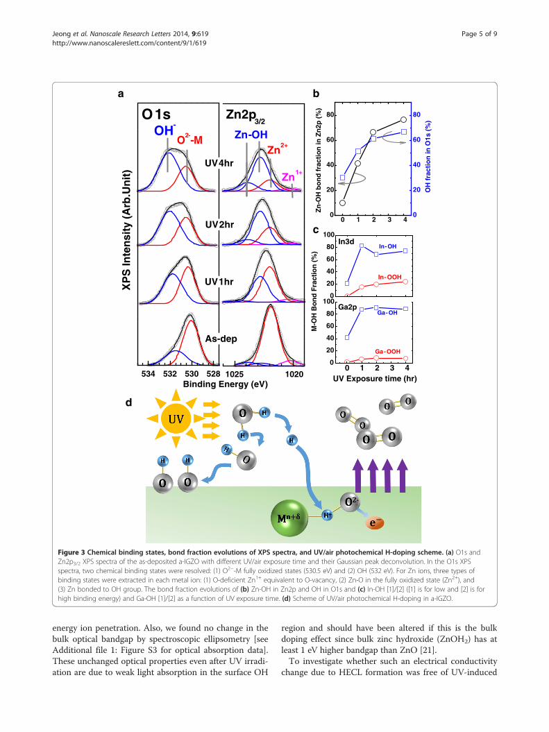
of HECL in terms of the change in UV-assisted surfacechemistry. Figure 3 shows narrow XPS scan spectra ofO1s and Zn2p3/2 chemical binding states in the as-deposited and UV-irradiated a-IGZO. In the O1s XPSspectrum, two chemical binding states were resolved: (i)O-metal (530.5 eV) and (ii) OH-M (532 eV) bindingstates (where M represents In, Ga, and Zn); these bindingstates agree with those reported in many previous reports[16,17]. For Zn ions, three types of binding states wereobserved: (i) O-deficient Zn1+ (1,020 eV), (ii) Zn2+ in itsfull oxidation state (1,021.7 eV), and (iii) Zn-OH-relatedbinding states (Zn-OH at 1,022.8 eV and Zn-OOH at1,023.9 eV). In and Ga ions were also found to displaythe identical O- and OH-related binding states [seeAdditional file 1: Figure S2 for In3d and Ga2p spectra].Each Zn2p binding state was consistent in the O1s andmetal XPS spectra, except O-deficient Zn1+ that originatesfrom the O-vacancy defect in the local metal-oxygen-bonding environment. The unsaturated O binding state inO-vacancy was not well resolved in the O1s spectra, whileZn1+ binding states were clearly resolved in the Zn2pspectra.UV-irradiated a-IGZO surfaces showed significant
changes in the metal-OH states. The metal-OH bondfractions normalized to the total areal intensity in eachmetal ion increase with increase in UV irradiation; thistrend corresponds to an increase in the OH bond frac-tion in the O1s XPS spectra corresponding to UV irradi-ation. The chemical reason for higher binding energiesof Zn-OH-related bonds is due to the higher group elec-tronegativity of OH compared to O. Although the groupelectronegativity of OH varies at 2.3 to 3.9 due to thelone pair π electrons with the remainder of the mol-ecule, Zn-OH configuration is subject to the highergroup electronegativity of OH than that of O (3.44) atleast since the binding energy of Zn-OH is higher thanZn-O in Zn2p spectra.The origin of significantly increased OH bond of
a-IGZO upon UV irradiation is related to the UV/air photo-chemistry. As described in the reaction scheme (Figure 3d),
due to UV photon energies used in this study, abundantexcited OH and H radicals are produced by photochem-ical water dissociation and react with the a-IGZO surface.Among those radical species, H is most effective for sur-face reaction due to the fast diffusion near the a-IGZOsurface. On the other hand, UV light itself is well knownto break O-metal bonds to create O-vacancy sites inmetal-oxygen bonds like Zn-O by the photocarrier-induced O desorption [18]. This provides the basis forsubstitutional H incorporation in addition to interstitialincorporation. Therefore, the proposed a-IGZO surfacereaction scheme under UV/air irradiation can be regardedas H incorporation to (1) O-vacancy substitutional sitesand (2) interstitial sites (due to a small size of H) andfinally appears as OH bonds. It was suggested that Hincorporation into a-IGZO always results in surface OHbond formation where conversion of H atoms to H+ ions(i.e., donor ions) increases the carrier concentrationgreatly as expressed in the following equation: H(ads) +Zn2+ + O2− (in a-IGZO)→H+(in lattice) + Zn2+ + O2− +e−→OH− (in a-IGZO) + Zn2+ + e−9. Here, similar reac-tions for In and Ga in addition to Zn can be considered.In order words, H atom donates excess electrons while be-ing the positively ionized donor ion in a-IGZO and isfinally converted to −OH or −O2−H+. This effect is alsoconfirmed in H-doped ZnO in the view of electronic bondstate, and interestingly, it was explained that an excesselectron initially occupies the high-lying Zn (4s)-H (1s)antibonding molecular orbital (MO) state above conduc-tion band (CB) edge of ZnO and deexcites to CB mini-mum states to be free carriers [19]. Similar chemicaldoping mechanism and coupling of excess electrons withIn/Ga (5s)-H (1s) is highly expected. Since electrons areconfined in s-orbital character MO state positioned at theedge of CB minimum, the carrier mobility should behigher than electrons trapped at the d-band dominantdeep donor level of O-vacancy. The OH formation ofa-IGZO upon H-induced n-type doping has been experi-mentally demonstrated in previous studies using thermalanneal and ion implantation [20]. However, the overalldoping effect with such doping methods is not so signifi-cant, and this was believed due to the doping effect com-pensation by the complicated interaction between looselybound O and H subject to the thermal diffusion through-out the bulk. Nevertheless, UV-induced H-doping in thisstudy reveals the remarkable effect of the insulator-to-metal transition. We regard that the key mechanismfor this distinguishable from other H-doping technique isrelated to double simultaneous photochemical reactions;O-vacancy creation and H incorporation, synergisticallyforming highly OH-rich a-IGZO surface not throughoutthe bulk. The surface localized H incorporation is inher-ent property of UV photochemistry done at roomtemperature free of significant thermal diffusion or high
Zn‐OH
UV4hr
UV2hr
UV1hr
Zn2+
OH‐
Zn2p3/2
XP
S In
ten
sity
(A
rb.U
nit
)O1s
O2‐‐M
As-dep
534 532 530 528 1025 1020
Zn1+
Binding Energy (eV)
0 1 2 3 40
20
40
60
80
Zn
‐OH
bo
nd
fra
ctio
n in
Zn
2p (
%)
0
20
40
60
80
OH
fra
ctio
n in
O1s
(%
)
0
20
40
60
80
100
Ga‐OOH
Ga‐OH
In‐OOH
In‐OH
Ga2pM
-OH
Bo
nd
Fra
ctio
n (
%)
UV Exposure time (hr)
In3d
0 1 2 3 40
20
40
60
80
100
a b
c
d
Figure 3 Chemical binding states, bond fraction evolutions of XPS spectra, and UV/air photochemical H-doping scheme. (a) O1s andZn2p3/2 XPS spectra of the as-deposited a-IGZO with different UV/air exposure time and their Gaussian peak deconvolution. In the O1s XPSspectra, two chemical binding states were resolved: (1) O2−-M fully oxidized states (530.5 eV) and (2) OH (532 eV). For Zn ions, three types ofbinding states were extracted in each metal ion: (1) O-deficient Zn1+ equivalent to O-vacancy, (2) Zn-O in the fully oxidized state (Zn2+), and(3) Zn bonded to OH group. The bond fraction evolutions of (b) Zn-OH in Zn2p and OH in O1s and (c) In-OH [1]/[2] ([1] is for low and [2] is forhigh binding energy) and Ga-OH [1]/[2] as a function of UV exposure time. (d) Scheme of UV/air photochemical H-doping in a-IGZO.
Jeong et al. Nanoscale Research Letters 2014, 9:619 Page 5 of 9http://www.nanoscalereslett.com/content/9/1/619
energy ion penetration. Also, we found no change in thebulk optical bandgap by spectroscopic ellipsometry [seeAdditional file 1: Figure S3 for optical absorption data].These unchanged optical properties even after UV irradi-ation are due to weak light absorption in the surface OH
region and should have been altered if this is the bulkdoping effect since bulk zinc hydroxide (ZnOH2) has atleast 1 eV higher bandgap than ZnO [21].To investigate whether such an electrical conductivity
change due to HECL formation was free of UV-induced

Figure 4 XRD pattern analysis for a-IGZO thin film phasessubjected to UV irradiation for different times. Regardless of UVirradiation time, all a-IGZO thin films exhibited an amorphous phase.This observation confirmed that electrical conductivity changes afterUV irradiation cannot be attributed to the formation of acrystalline structure.
10 5 0 5 10 15 2010
11
1010
109
108
107
106
105
104
103
10 5 0 5 10 15 200.0
0.1
0.2
Dra
in c
urre
nt (
A)
Gate voltage (V)
HECL_60 mHECL_40 mHECL_20 mHECL_0 m
Dra
in c
urre
nt (
mA
)
Gate voltage (V)
a
Figure 5 Transfer characteristics and Ids-Vds curves of DAL TFTs with vof DAL TFTs with varying HECL length. On-current increased monotonicallyfigure is the linear scale curve. This observation confirmed that superior eleno change in the off-current, as a semiconducting gap with a width of 10
Jeong et al. Nanoscale Research Letters 2014, 9:619 Page 6 of 9http://www.nanoscalereslett.com/content/9/1/619
bulk phase change in the a-IGZO thin films, X-ray dif-fraction measurements were performed to analyze thecrystallinity of thin films after UV irradiation for varioustimes. Figure 4 shows the XRD patterns of a-IGZO thinfilms deposited at room temperature using a sputteringmethod and UV irradiation for various times. The XRDpatterns do not indicate a crystalline peak regardless ofthe UV irradiation time; thus, it can be stated as XRDamorphous. Nevertheless, XRD is unable to detect ananocrystallinity (nc) at the length of ordering scale lessthan approximately 4 nm [22]. To investigate the effectsof HECL formation for TFT performance, we comparedthe transfer characteristics of TFTs according to changesin HECL length in the active layer (Figure 5). Eachtransfer curve shows the results measured under thesame conditions of Vds =18 V and TFT drain current inthe saturation region (Vds ≥ Vgs −Vth) as represented byEquation 1
Ids ¼ WμsatCi
2LV gs−V th� �2 ð1Þ
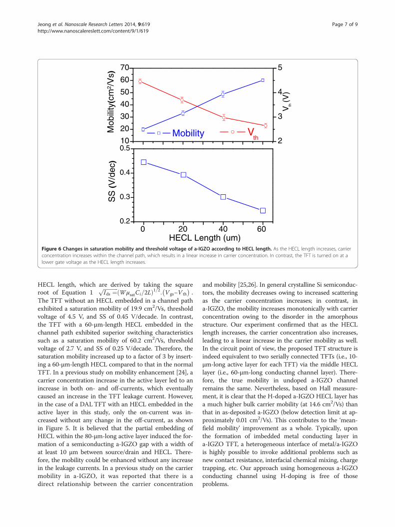
where μsat is the saturation mobility, Vth is the thresholdvoltage, L is the channel length, W is the channel width,and Ci is the electrostatic capacity of a dielectric layerper unit area [23]. The systematic increase in the draincurrent level is observed with UV irradiation time, andthis trend is also confirmed in Ids-Vds curve (Figure 5b).Figure 6 shows changes in the threshold voltage, satur-
ation mobility, and subthreshold swing (SS) with the
0 5 10 15 20 25 300.0
0.1
0.2
0 m
40 m
20 m
Source-Drain Voltage (V)
HECL 60 m
b
arying HECL length. (a) Transfer characteristics and (b) Ids-Vds curvesas the HECL length increased within the same channel. The insetctrical properties are obtained with an increase in the on-current andμm exists between source/drain and HECL.
10
20
30
40
50
60
70
2
3
4
5
Mob
ility
(cm
2 /V
s)
Mobility
V th(V
)
Vth
0.2
0.3
0.4
0.5
SS
(V
/dec
)
HECL Length (um)0 20 40 60
Figure 6 Changes in saturation mobility and threshold voltage of a-IGZO according to HECL length. As the HECL length increases, carrierconcentration increases within the channel path, which results in a linear increase in carrier concentration. In contrast, the TFT is turned on at alower gate voltage as the HECL length increases.
Jeong et al. Nanoscale Research Letters 2014, 9:619 Page 7 of 9http://www.nanoscalereslett.com/content/9/1/619
HECL length, which are derived by taking the squareroot of Equation 1
ffiffiffiffiffiffiffiffiffiffiffiIds ¼
pWμsatCi=2Lð Þ1=2: V gs−V th
� �.
The TFT without an HECL embedded in a channel pathexhibited a saturation mobility of 19.9 cm2/Vs, thresholdvoltage of 4.5 V, and SS of 0.45 V/decade. In contrast,the TFT with a 60-μm-length HECL embedded in thechannel path exhibited superior switching characteristicssuch as a saturation mobility of 60.2 cm2/Vs, thresholdvoltage of 2.7 V, and SS of 0.25 V/decade. Therefore, thesaturation mobility increased up to a factor of 3 by insert-ing a 60-μm-length HECL compared to that in the normalTFT. In a previous study on mobility enhancement [24], acarrier concentration increase in the active layer led to anincrease in both on- and off-currents, which eventuallycaused an increase in the TFT leakage current. However,in the case of a DAL TFT with an HECL embedded in theactive layer in this study, only the on-current was in-creased without any change in the off-current, as shownin Figure 5. It is believed that the partial embedding ofHECL within the 80-μm-long active layer induced the for-mation of a semiconducting a-IGZO gap with a width ofat least 10 μm between source/drain and HECL. There-fore, the mobility could be enhanced without any increasein the leakage currents. In a previous study on the carriermobility in a-IGZO, it was reported that there is adirect relationship between the carrier concentration
and mobility [25,26]. In general crystalline Si semiconduc-tors, the mobility decreases owing to increased scatteringas the carrier concentration increases; in contrast, ina-IGZO, the mobility increases monotonically with carrierconcentration owing to the disorder in the amorphousstructure. Our experiment confirmed that as the HECLlength increases, the carrier concentration also increases,leading to a linear increase in the carrier mobility as well.In the circuit point of view, the proposed TFT structure isindeed equivalent to two serially connected TFTs (i.e., 10-μm-long active layer for each TFT) via the middle HECLlayer (i.e., 60-μm-long conducting channel layer). There-fore, the true mobility in undoped a-IGZO channelremains the same. Nevertheless, based on Hall measure-ment, it is clear that the H-doped a-IGZO HECL layer hasa much higher bulk carrier mobility (at 14.6 cm2/Vs) thanthat in as-deposited a-IGZO (below detection limit at ap-proximately 0.01 cm2/Vs). This contributes to the ‘mean-field mobility’ improvement as a whole. Typically, uponthe formation of imbedded metal conducting layer ina-IGZO TFT, a heterogeneous interface of metal/a-IGZOis highly possible to invoke additional problems such asnew contact resistance, interfacial chemical mixing, chargetrapping, etc. Our approach using homogeneous a-IGZOconducting channel using H-doping is free of thoseproblems.
Jeong et al. Nanoscale Research Letters 2014, 9:619 Page 8 of 9http://www.nanoscalereslett.com/content/9/1/619
In addition to the mobility enhancement, it was con-firmed that TFTs can be turned on at a lower gate voltagewhen the carrier concentration increases, and the thresh-old voltage is gradually lowered owing to the increasedlength of embedded HECL within a channel path. The re-lationship between the carrier concentration and thresh-old voltage has been reported in a previous study [4].The concurrent changes in crucial TFT parameters suchas saturation mobility and Vth are closely related tochemical changes of a-IGZO by UV-induced H-doping.As shown in Figure 3d, the high OH fraction is equiva-lent to a surface H-doping effect or hydroxide formationon a-IGZO. Thus, the surface potential of an HECL ledby UV photochemistry leads to a relatively negative Vth
shift in TFT devices.Additionally, it can be found that intensity of the O-
deficient Zn1+ (1,020 eV) peak is decrease with in UV ir-radiation, as shown in Figure 3. It means that O-vacancydefects acting trap site in the local metal-oxygen-bondingenvironment decreased. Therefore, increase of HECLlength leads to the decrease in the density of trap site atthe whole active channel layer. In general, SS value isclosely related to the density of trap site in active layer ofTFTs [27]. Hence, as the HECL length increases, the SSvalue of the device also improves.
ConclusionsIn this study, we fabricated DAL TFTs via a new ap-proach called permanent photochemical doping to en-hance the mobility of existing bottom-gate-structureTFTs. Different from existing DAL TFT mobility en-hancement methods, the structure resulting from this ap-proach employs the same phase and material; thus,degradation in electrical properties due to physical inter-face formation or band offset does not occur. The chem-ical origin of permanent optical doping in HECL wasfound as UV photochemistry induced intensive and uni-form surface H-doping of a-IGZO proved by XPS. More-over, the effects of changes in the HECL length on thechannel path were investigated. The obtained resultsshowed that the mobility increased monotonically as thelength of the embedded HECL increased. This result wasattributed to the carrier concentration increase in the ac-tive layer channel area triggered by changes in the HECLlength. Finally, the highest mobility of 60.2 cm2/Vs wasobtained when a 60-μm-long HECL was embedded in an80-μm-long channel path. This observation confirmedthat an HECL length 75% of the total active layer lengthresults in high-performance characteristics for materialswith 200% improvement in mobility: a threshold voltageof 2.7 V, SS of 0.25 V/decade, and an on/off ratio of 107.Moreover, the leakage current level was maintained at10−11 A. All these significant improvements in a-IGZOTFTs are explained by the effective n-doping in HECL by
UV-induced H-incorporation on the surface, confirmedby OH-rich surface of a-IGZO. Surface H-doping resultsin a high electron donation in the HECL even foramorphous a-IGZO without any heat treatment to im-prove crystallinity and dopant activation. Therefore,owing to its great simplicity, the comprehensive per-formance improvement achievable, and stability, thedoping technique proposed herein can be effectively uti-lized for large-scale a-IGZO TFT arrays employed inflat-panel displays. The applicability of the H-dopingtechnique proposed in this study can be extended if itbecomes possible to carry out selective UV irradiationalong with in situ a-IGZO deposition through improve-ments in process equipment in the future.
Additional file
Additional file 1: Dual active layer a-IGZO TFT via homogeneousconductive layer formation by photochemical H-doping. Figure S1.Hall measurement results (carrier concentration and Hall mobility) as afunction of air aging-time. Figure S2. In3d and Ga2p XPS data of theas-deposited and UV-exposed a-IGZO with Gaussian peak deconvolution.Figure S3. Absorption coefficient spectra for the as-deposited andUV-irradiated a-IGZO taken by spectroscopic ellipsometry analysis.
Competing interestsThe authors declare that they have no competing interests.
Authors’ contributionsSJ, HS, and DC designed the experiments. SJ, MK, and SL carried out theexperiments and tested the devices. SJ, HS, and DC analyzed the data andwrote the manuscript. All authors read and approved the final manuscript.
AcknowledgementsThis research was supported by the Basic Science Research Program throughthe National Research Foundation of Korea (NRF) funded by the Ministry ofScience, ICT and Future Planning (2013R1A1A2064715) and also supportedby the Basic Science Program (NRF-2012R1A1A1005014) through theNational Research Foundation (NRF) of the Ministry of Science, ICT andFuture Planning.
Received: 1 September 2014 Accepted: 24 October 2014Published: 18 November 2014
References1. Bardsley JN: International OLED technology roadmap. IEEE J Sel Top Quant
Electron, IEEE Journal of 2004, 10:3–9.2. Nomura K, Ohta H, Takagi A, Kamiya T, Hirano M, Hosono H: Room-
temperature fabrication of transparent flexible thin-film transistors usingamorphous oxide semiconductors. Nature 2004, 432:488–492.
3. Yabuta H, Sano M, Abe K, Aiba T, Den T, Kumomi H, Nomura K, Kamiya T,Hosono H: High-mobility thin-film transistor with amorphous InGaZnO4channel fabricated by room temperature rf-magnetron sputtering. ApplPhys Lett 2006, 89. 112123-1-112123-3.
4. Jeong JK, Jeong JH, Yang HW, Park J-S, Mo Y-G, Kim HD: High performancethin film transistors with cosputtered amorphous indium gallium zincoxide channel. Appl Phys Lett 2007, 91. 113505-1-113505-3.
5. Park J-S, Kim H, Kim I-D: Overview of electroceramic materials for oxidesemiconductor thin film transistors. J Electroceram 2014, 32:117–140.
6. Chiang HQ, McFarlane BR, Hong D, Presley RE, Wager JF: Processing effectson the stability of amorphous indium gallium zinc oxide thin-filmtransistors. J Non-Cryst Solids 2008, 354:2826–2830.
7. Suresh A, Gollakota P, Wellenius P, Dhawan A, Muth JF: Transparent, highmobility InGaZnO thin films deposited by PLD. Thin Solid Films 2008,516:1326–1329.

Jeong et al. Nanoscale Research Letters 2014, 9:619 Page 9 of 9http://www.nanoscalereslett.com/content/9/1/619
8. Se IO, Godeuni C, Hyunsang H, Wu L, Jae-Hyung J: Hydrogenated IGZOthin-film transistors using high-pressure hydrogen annealing. IEEE TransElectron Dev 2013, 60:2537–2541.
9. Kamiya T, Nomura K, Hosono H: Origins of high mobility and lowoperation voltage of amorphous oxide TFTs: electronic structure,electron transport, defects and doping*. J Display Technol 2009,5:468–483.
10. Zan H-W, Yeh C-C, Meng H-F, Tsai C-C, Chen L-H: Achieving high field-effect mobility in amorphous indium-gallium-zinc oxide by capping astrong reduction layer. Adv Mater 2012, 24:3509–3514.
11. Hosono H: Ionic amorphous oxide semiconductors: Material design,carrier transport, and device application. J Non-Cryst Solids 2006,352:851–858.
12. Iwasaki T, Itagaki N, Den T, Kumomi H, Nomura K, Kamiya T, Hosono H:Combinatorial approach to thin-film transistors using multicomponentsemiconductor channels: an application to amorphous oxidesemiconductors in In–Ga–Zn–O system. Appl Phys Lett 2007, 90.242114-1242114-3.
13. Kim ES, Ryu MK, Son KS, Kim TS, Lee K-H, Park KB, Park JS, Maeng WJ, KimHS, Seon JB, Choi W, Lee S: Metal-channel-aided oxide thin film transistor.Meeting Abstracts 2010, 1819:MA2010–02.
14. Kim MJ, Choi D-k: Effect of enhanced-mobility current path on the mobilityof AOS TFT. Microelectron Reliab 2012, 52:1346–1349.
15. Flores F, Tejedor C: Energy barriers and interface states atheterojunctions. J Phys C Solid State Phys 1979, 12:731.
16. Mosbacker HL, Strzhemechny YM, White BD, Smith PE, Look DC, ReynoldsDC, Litton CW, Brillson LJ: Role of near-surface states in ohmic-Schottkyconversion of Au contacts to ZnO. Appl Phys Lett 2005, 87.012102-1-012102-3.
17. Tay YY, Li S, Sun CQ, Chen P: Size dependence of Zn 2p3/2 bindingenergy in nanocrystalline ZnO. Appl Phys Lett 2006, 88. 173118-1-173118-3.
18. Lim SJ, Kim J-M, Kim D, Lee C, Park J-S, Kim H: The effects of UV exposureon plasma-enhanced atomic layer deposition ZnO thin film transistor.Electrochem Solid-State Lett 2010, 13:H151–H154.
19. Janotti A, Van de Walle CG: Hydrogen multicentre bonds. Nat Mater 2007,6:44–47.
20. Nomura K, Kamiya T, Hosono H: Effects of diffusion of hydrogen andoxygen on electrical properties of amorphous oxide semiconductor,In-Ga-Zn-O. ECS J Solid State Sci Technol 2013, 2:P5–P8.
21. Bang S, Lee S, Ko Y, Park J, Shin S, Seo H, Jeon H: Photocurrent detectionof chemically tuned hierarchical ZnO nanostructures grown on seedlayers formed by atomic layer deposition. Nanoscale Res Lett 2012, 7:290.
22. Seo H, Lucovsky G, Fleming LB, Ulrich MD, Lüning J, Koster G, Geballe TH:Length scales for coherent π-bonding interactions in complex high-koxide dielectrics and their interfaces. Microelectron Eng 2007,84:2298–2301.
23. Schroder DK: Semiconductor Material and Device Characterization. Hoboken,New Jersey, United States of America: Wiley-Interscience; 2006.
24. Tsao SW, Chang TC, Huang SY, Chen MC, Chen SC, Tsai CT, Kuo YJ, ChenYC, Wu WC: Hydrogen-induced improvements in electrical characteristicsof a-IGZO thin-film transistors. Solid State Electron 2010, 54:1497–1499.
25. Nomura K, Kamiya T, Ohta H, Ueda K, Hirano M, Hosono H: Carriertransport in transparent oxide semiconductor with intrinsic structuralrandomness probed using single-crystalline InGaO3(ZnO)5 films. ApplPhys Lett 2004, 85:1993–1995.
26. Takagi A, Nomura K, Ohta H, Yanagi H, Kamiya T, Hirano M, Hosono H:Carrier transport and electronic structure in amorphous oxidesemiconductor, a-InGaZnO4. Thin Solid Films 2005, 486:38–41.
27. Park JS, Jeong JK, Chung HJ, Mo YG, Kim HD: Electronic transportproperties of amorphous indium-gallium-zinc oxide semiconductor uponexposure to water. Appl Phys Lett 2008, 92. 072104-1–072104-3.
doi:10.1186/1556-276X-9-619Cite this article as: Jeong et al.: Dual active layer a-IGZO TFT viahomogeneous conductive layer formation by photochemical H-doping.Nanoscale Research Letters 2014 9:619.
Submit your manuscript to a journal and benefi t from:
7 Convenient online submission
7 Rigorous peer review
7 Immediate publication on acceptance
7 Open access: articles freely available online
7 High visibility within the fi eld
7 Retaining the copyright to your article
Submit your next manuscript at 7 springeropen.com