Embed Size (px)
Citation preview

CHR2270-QRG
Ref. : DSCHR2270-QRG1180 - 30 Jun 21 1/18 Specifications subject to change without notice United Monolithic Semiconductors S.A.S.
Bât. Charmille - Parc Mosaic - 10, Avenue du Québec - 91140 VILLEBON-SUR-YVETTE - France Tel.: +33 (0) 1 69 86 32 00 - Fax: +33 (0) 1 69 86 34 34 - www.ums-rf.com
5.8GHz Transponder SiGe Monolithic Microwave IC in SMD leadless package
Description
The CHR2270-QRG is an integrated transponder circuit, manufactured in SiGe technology and designed to be compatible with ETSI ES 200 674 and EN 300 674 dedicated to short-range communications at 5.8GHz. It includes all the RF functions for bi-directional transmission and digital interfaces to controller, with high flexibility for performances customization. Three modes are implemented: STANDBY: ultra-low current AM detector, with integrated RF filtering, providing a selective wake-up signal on SB_out & SB_CPT outputs. These outputs are active when an AM modulated RF signal is applied to the RF input with either ETSI ES 200 674 or EN 300 674 patterns. DOWNLINK: low current AM detector, with optimized IF bandwidth, providing the demodulated data at the Data_out output. UPLINK: multipliers based on passive reflective mixers operating either in phase or amplitude modulation. Main Features 5.8GHz ISM band operating frequency Single RF port and antenna for compact system Integrated wake-up circuit with additional selective output 3V battery bias voltage range oriented with Ultra low Standby current and IDLE mode Adjustable Standby time & threshold parameters with 2 bits wake-up sensitivity digital control High wake-up selectivity High AM detection sensitivity for Downlink Adjustable Downlink parameters Downlink RF input power level monitoring Digital output interfaces CMOS compatible Wide Uplink and Downlink IF bandwidth High performance phase and amplitude modulator for low Uplink losses Uplink gain control Integrated loop for emitted RF spectrum power limitation -40°C to +90°C temperature range ESD protected
UMS CHR2270
YYWW

CHR2270-QRG 5.8GHz Transponder
Ref. : DSCHR2270-QRG1180 - 30 Jun 21 2/18 Specifications subject to change without notice
Bât. Charmille - Parc Mosaic - 10, Avenue du Québec - 91140 VILLEBON-SUR-YVETTE - France Tel.: +33 (0) 1 69 86 32 00 - Fax: +33 (0) 1 69 86 34 34 - www.ums-rf.com
High performances small leadless plastic package RoHS compliant Main Electrical Characteristics
Full operating range
Symbol Parameter Test conditions Min Typ Max Unit
Vcc Bias voltage +2.7 +3 +3.2 V
Top Operating Temperature range -25 +25 +90 °C
Fop Operating RF frequency range 5.72 5.8 5.88 GHz
BW_rf RF bandwidth 40 MHz
RL_rf (*) RF return loss 50 Ω (1) UL_Gc_v<0.1V
-12 -8 dB
DP_v Digital ports input voltage high low
Vcc-0.1 0
Vcc +0.1
V
WK_in_v WK_in port input voltage high low
+2.7 -0.1
+3 0
+3.2 +0.1
V V
WK_in_imp (*) WK_in port impedance 1350
10
Ω pF
WK_in_t_d (*) WK_in recovery time to receive WK_in ‘0’ to ‘1’ 30 µs
WK_in_t_u (*) WK_in recovery time to transmit WK_in ‘0’ to ‘1’ 10 µs
T/R_imp (*) T/R input port impedance 100 kΩ
pF 5 10
T/R_t (*) Transmit to Receive recovery time 30 µs
R/T_t (*) Receive to Transmit recovery time
AGC=’0’ AGC=’1’ 0.5
20 1 30 µs

5.8GHz Transponder CHR2270-QRG
Ref. : DSCHR2270-QRG1180 - 30 Jun 21 3/18 Specifications subject to change without notice
Bât. Charmille - Parc Mosaic - 10, Avenue du Québec - 91140 VILLEBON-SUR-YVETTE - France Tel.: +33 (0) 1 69 86 32 00 - Fax: +33 (0) 1 69 86 34 34 - www.ums-rf.com
All modes (Full operating range)
Symbol Parameter Test conditions Min Typ Max Unit
Vcc Bias voltage +2.7 3 +3.2 V Top Operating Temperature range -25 25 90 °C op Operating RF frequency range 5.72 5.8 5.88 GHz
BW_rf RF bandwidth 40 MHz
RL_rf (*) RF return loss 50 Ω (1)
-12 -8 dB UL_Gc_v<0.1V
DP_v Digital ports input voltage high
Vcc-0.1
Vcc
V low 0 +0.1
WK_in_v WK_in port input voltage high
+2.7 3 +3.2 V
low -0.1 0 +0.1 V
WK_in_imp (*) WK_in port impedance 1350
Ω
10 pF WK_in_t_d (*) WK_in recovery time to receive WK_in ‘0’ to ‘1’ 30 µs WK_in_t_u (*) WK_in recovery time to transmit WK_in ‘0’ to ‘1’ 10 µs
T/R_imp (*) T/R input port impedance 100 kW
5 10 pF T/R_t (*) Transmit to Receive recovery time 30 µs
R/T_t (*) Receive to Transmit recovery time AGC=’0’
0.5 1
µs AGC=’1’ 20 30
(1) An external matching may be required to optimise performances versus substrate height. (*) Note : Min & Max values include technological spreads, supply & temperature range effect.

CHR2270-QRG 5.8GHz Transponder
Ref. : DSCHR2270-QRG1180 - 30 Jun 21 4/18 Specifications subject to change without notice
Bât. Charmille - Parc Mosaic - 10, Avenue du Québec - 91140 VILLEBON-SUR-YVETTE - France Tel.: +33 (0) 1 69 86 32 00 - Fax: +33 (0) 1 69 86 34 34 - www.ums-rf.com
STANDBY mode: T/R=‘0’, MT=’0’, MOD=’0’, WK_in=‘low’
Symbol Parameter Test conditions Min Typ Max Unit
SB_load Standby SB_out & SB_CPT output ports load impedance
1
MW 10 pF
SB_v (*)
Standby SB_out & SB_CPT output ports DC voltage
V
high level (1) Vcc-0.2 Vcc
low level 0 +0.2
RF_sb_out_bw Amplitude modulation frequency of RF for SB_out wake-up 250 500 kHz
RF_sb_CPT_am Amplitude modulation frequency of RF for SB_CPT wake-up 240 250 260 kHz
RF_sb_cf (*) Amplitude modulation frequency of RF on RF port for non-wake-up at any Fop
RF_sb_p_max<0dBm DC 10 kHz m=1
C_Delay=any pF
RF_sb_p_min (*) Amplitude modulated RF minimum input power on RF port for wake-up
(2) -49 -44 -39 dBm IDLE=”0”
(4)
RF_sb_p_ds (*) RF_sb_p_min digital step IDLE=”0” 1.5 2 2.5 dB
SB_Sn_imp RF_sb_p digital setting ports impedance
10
MW 3 pF
RF_sb_p_max (*) Amplitude modulated RF maximum input power on RF port for wake-up (2)
-10 -6 dBm
SB_wk_delay (*) Time delay for wake-up -3 12.5 25 50 µs SB_CPT_delay (*) Time delay for CPT wake-up 35 70 140 µs
IDLE_imp IDLE setting port impedance 10
MW
3 pF IDLE_delay (*) IDLE recovery delay ”1” to “0” @ RF_sb_p_min 1 ms
Vcc_sb_i (*) Standby DC current
Without RF input signal
3.8 8
µA
(RF_sb_p<-35dBm & SB_out=’1’) 40 60
(RF_sb_p >-20dBm &
SB_out=’0’) 80 120
IDLE=”1” any RF 1.8 4 (1) Wake-up signal is given by a transition on SB_v from low level to high-level state. (2) Total received power of the modulated signal (modulation index = 0.5). (3) C_Delay unconnected (no external capacitor). (4) SB_Sn & R (on Sens_SB) as recommended to match -44dBm typical on a given wafers lot. (*) Note: Min & Max values include technological spreads, supply & temperature range effect.

5.8GHz Transponder CHR2270-QRG
Ref. : DSCHR2270-QRG1180 - 30 Jun 21 5/18 Specifications subject to change without notice
Bât. Charmille - Parc Mosaic - 10, Avenue du Québec - 91140 VILLEBON-SUR-YVETTE - France Tel.: +33 (0) 1 69 86 32 00 - Fax: +33 (0) 1 69 86 34 34 - www.ums-rf.com
DOWNLINK mode: IDLE=’0’, T/R=‘0’, MOD=’0’, WK_in=‘high’
Symbol Parameter Test conditions Min Typ Max Unit
Data_out_load Downlink output port load impedance
1
MW 10 pF
Data_out_v (*)
Downlink output port DC voltage
high level (1) WK_in-0.2 WK_in V
low level (1) 0 +0.2 V
Data_out_f Amplitude demodulation frequency 250 1000 kHz
Data_out_f_3dB Amplitude demodulation 3dB frequency band 50 2000 kHz
Data_out_dc (*) Data_out signal duty cycle 42.5 50 57.5 %
RF_dl_p_min (*) Amplitude modulated RF minimum input power on RF port for downlink
(2) -44 -39 dBm
UL_Gc_v<0.1V
RF_dl_p_max (*) Amplitude modulated RF maximum input power on RF port for downlink
(2) -10 -6 dBm
DL_Pd_v (*) RF port incident power detection voltage (DL_Pd DC voltage) (3) +0.1 WK_in
-0.25 V
Pd_RF_p RF port incident power detection range -40 -10 dBm
Pd_delay (*) RF port incident power detection delay 10 µs
DL_Pd_load DL_Pd output port load impedance
1
MW 10 pF
Pd_Ref_v (*) Power detection reference voltage (Pd_Ref DC voltage) (3) WK_in
-1.25 WK_in
-1 WK_in-0.75 V
Pd_Ref_load Pd_Ref output port load impedance
1
MW 10 pF
Pd_diff_offset (*) Pd_diff initial offset (3) RF_dl_p_min 0 +0.15 V
Pd_diff_15 (*) Pd_diff guaranteed DC detection voltage (3)
RF_dl_p = +0.2 +0.6 V -15dBm
UL_Gc_v<0.1V WK_in_i (*) WK_in DC current 0.25 2 mA
(1) Data_out is valid only in the downlink window specified above, and noise may produce inconsistent data below RF_dl_p_min power level. (2) Total received power of the modulated signal (modulation index = 0.5). (3) Pd_diff = Pd_Ref_v-DL_Pd_v = function (RF_dl_p), RF input signal modulated or not. (*) Note: Min & Max values include technological spreads, supply & temperature range effect.
CHR2270-QRG 5.8GHz Transponder
Ref. : DSCHR2270-QRG1180 - 30 Jun 21 6/18 Specifications subject to change without notice
Bât. Charmille - Parc Mosaic - 10, Avenue du Québec - 91140 VILLEBON-SUR-YVETTE - France Tel.: +33 (0) 1 69 86 32 00 - Fax: +33 (0) 1 69 86 34 34 - www.ums-rf.com
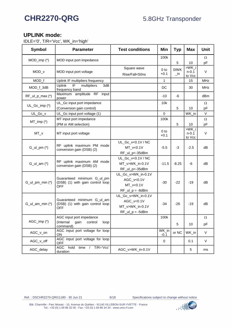
UPLINK mode: IDLE=’0’, T/R=‘Vcc’, WK_in=‘high’
Symbol Parameter Test conditions Min Typ Max Unit
MOD_imp (*) MOD input port impedance 100k Ω
5 10 pF
MOD_v MOD input port voltage Square wave 0 to
+0.1 0/WK_in
>WK_in-0.1 to Vcc
V Rise/Fall<50ns
MOD_f Uplink IF multipliers frequency 1 15 MHz
MOD_f_3dB Uplink IF multipliers 3dB frequency band DC 30 MHz
RF_ul_p_max (*) Maximum amplitude RF input power -10 -6 dBm
UL_Gc_imp (*) UL_Gc input port impedance
10k Ω
(Conversion gain control) 5 10 pF UL_Gc_v UL_Gc input port voltage (1) 0 WK_in V
MT_imp (*) MT input port impedance
100k Ω
(PM or AM selection) 5 10 pF
MT_v MT input port voltage 0 to +0.1
>WK_in-0.1 to Vcc
V
G_ul_pm (*) RF uplink maximum PM mode conversion gain (DSB) (2)
UL_Gc_v<0.1V / NC -5.5 -3 -2.5 dB MT_v<0.1V
RF_ul_p<-35dBm
G_ul_am (*) RF uplink maximum AM mode conversion gain (DSB) (2)
UL_Gc_v<0.1V / NC -11.5 -8.25 -6 dB MT_v>WK_in-0.1V
RF_ul_p<-35dBm
G_ul_pm_min (*) Guaranteed minimum G_ul_pm (DSB) (1) with gain control loop OFF
UL_Gc_v>WK_in-0.1V
-30 -22 -19 dB AGC_v<0.1V MT_v<0.1V
RF_ul_p = -8dBm
G_ul_am_min (*) Guaranteed minimum G_ul_am (DSB) (1) with gain control loop OFF
UL_Gc_v>WK_in-0.1V
-34 -26 -19 dB AGC_v<0.1V
MT_v>WK_in-0.1V RF_ul_p = -5dBm
AGC_imp (*) AGC input port impedance
100k Ω
(Internal gain control loop command)
5 10 pF
AGC_v_on AGC input port voltage for loop ON WK_in
-0.1 or NC WK_in V
AGC_v_off AGC input port voltage for loop OFF 0 0.1 V
AGC_delay AGC hold time / T/R=’Vcc’ duration AGC_v>WK_in-0.1V 5 ms

5.8GHz Transponder CHR2270-QRG
Ref. : DSCHR2270-QRG1180 - 30 Jun 21 7/18 Specifications subject to change without notice
Bât. Charmille - Parc Mosaic - 10, Avenue du Québec - 91140 VILLEBON-SUR-YVETTE - France Tel.: +33 (0) 1 69 86 32 00 - Fax: +33 (0) 1 69 86 34 34 - www.ums-rf.com
Symbol Parameter Test conditions Min Typ Max Unit
G_ul_pm_min_l (*) Guaranteed minimum G_ul_pm (DSB) (1) with gain control loop ON
UL_Gc NC
-32 -25 -15 dB
AGC_v>WK_in-0.1V MT_v<0.1V
RF_ul_p = -8dBm Appropriate R on DL_Pd to PD_Ref or Sens_AGC for
Typ
G_ul_am_min_l (*) Guaranteed minimum G_ul_am (DSB) (1) with gain control loop ON
UL_Gc NC
-33 -26 -16 dB
AGC_v>WK_in-0.1V MT_v>WK_in-0.1V RF_ul_p = -5dBm
Appropriate R on DL_Pd to PD_Ref or Sens_AGC for
Typ
UL_TSM RF emitted maximum spurious level in 500kHz Rbw
@ Fop +/- 1.5, 2, 3, 3.5, 6.5, 7 MHz excluding Fop +/-
MOD_f -39 dBm UL_Gc_v>WK_in-0.1V
Sub - carrier is pseudo random modulated as
defined by ETSI WK_in_i (*) WK_in DC current 1 2 mA
(1) G_ul = Function(UL_Gc_v) (2) G_ul = Emitted_Power(RF port @ (Fop + MOD_f)) + Emitted_Power(RF port @ (Fop - MOD_f)) - Incident_Power(RF port @ Fop) (*) Note : Min & Max values include technological spreads, supply & temperature range effect.

CHR2270-QRG 5.8GHz Transponder
Ref. : DSCHR2270-QRG1180 - 30 Jun 21 8/18 Specifications subject to change without notice
Bât. Charmille - Parc Mosaic - 10, Avenue du Québec - 91140 VILLEBON-SUR-YVETTE - France Tel.: +33 (0) 1 69 86 32 00 - Fax: +33 (0) 1 69 86 34 34 - www.ums-rf.com
Absolute Maximum Ratings (1) Tamb.= +25°C Symbol Parameter Values Unit
Vcc Bbias voltage >-0.3 & <4 V
WK_in_v WK_in input port voltage >-0.3 & <4 & <Vcc+0.3 V
T/R_v Transmit / Receive input voltage >-0.3 & <4 & <Vcc+0.3 V
MOD_v MOD port input voltage >-0.3 & <4 & <Vcc+0.3 V
RF_dl_p RF_ul_p
Maximum Standby, Downlink and Uplink RF input power on RF port +5 dBm
Top Operating temperature range -40 to +90 °C Tstg Storage temperature range -50 to +150 °C
(1) Operation of this device above anyone of these parameters may cause permanent damage.

5.8GHz Transponder CHR2270-QRG
Ref. : DSCHR2270-QRG1180 - 30 Jun 21 9/18 Specifications subject to change without notice
Bât. Charmille - Parc Mosaic - 10, Avenue du Québec - 91140 VILLEBON-SUR-YVETTE - France Tel.: +33 (0) 1 69 86 32 00 - Fax: +33 (0) 1 69 86 34 34 - www.ums-rf.com
Timing characteristics Downlink mode
Parameter MIN TYP MAX UNIT Condition Tsb_wake_delay 12.5 25 50 µs Cdelay unconnected
Tdelay 0 t µs Capacitor (k*t) pF on Cdelay
Tsb-r 10 µs Tsb_cpt_delay 35 70 140 µs
Tsb_cpt-r 10 µs Twk_in-r 0 µs Tdata-s 1 µs Tdata-sw 30 µs Tdata-str 30 µs
Tdata-r 1 µs
Data noise filters threshold settled with R
on Sens_DT input to GND
modulated carrier Un-modulated carrier Un-modulated carrier
DATA_OUT
RF input
WK_IN
SB_OUT
Tsb_wake_del
Tdelay Tsb-r
Twk_in-r
T/R
Tdata-s Tdata-r Tdata-str Tdata-sw

CHR2270-QRG 5.8GHz Transponder
Ref. : DSCHR2270-QRG1180 - 30 Jun 21 10/18 Specifications subject to change without notice
Bât. Charmille - Parc Mosaic - 10, Avenue du Québec - 91140 VILLEBON-SUR-YVETTE - France Tel.: +33 (0) 1 69 86 32 00 - Fax: +33 (0) 1 69 86 34 34 - www.ums-rf.com
Timing characteristics Uplink mode
Parameter MIN TYP MAX UNIT Condition
Tup-sw 10 µs Tagci 10 µs Tagch 5000 µs Tmod-s 30 µs Trf-sr 1 µs Trf-r 1 µs Ttr-r 1 µs
MOD
Tmod-s
Ttr-r Tagci Tagch
modulated carrier Un-modulated carrier Un-modulated carrier RF
T/R
WK_IN
Trf-sr Trf-r
Tup-sw
5.8GHz Transponder CHR2270-QRG
Ref. : DSCHR2270-QRG1180 - 30 Jun 21 11/18 Specifications subject to change without notice
Bât. Charmille - Parc Mosaic - 10, Avenue du Québec - 91140 VILLEBON-SUR-YVETTE - France Tel.: +33 (0) 1 69 86 32 00 - Fax: +33 (0) 1 69 86 34 34 - www.ums-rf.com
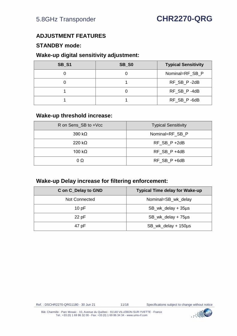
ADJUSTMENT FEATURES STANDBY mode: Wake-up digital sensitivity adjustment:
SB_S1 SB_S0 Typical Sensitivity
0 0 Nominal=RF_SB_P
0 1 RF_SB_P -2dB
1 0 RF_SB_P -4dB
1 1 RF_SB_P -6dB
Wake-up threshold increase:
R on Sens_SB to +Vcc Typical Sensitivity
390 kΩ Nominal=RF_SB_P
220 kΩ RF_SB_P +2dB
100 kΩ RF_SB_P +4dB
0 Ω RF_SB_P +6dB
Wake-up Delay increase for filtering enforcement: C on C_Delay to GND Typical Time delay for Wake-up
Not Connected Nominal=SB_wk_delay
10 pF SB_wk_delay + 35µs
22 pF SB_wk_delay + 75µs
47 pF SB_wk_delay + 150µs

CHR2270-QRG 5.8GHz Transponder
Ref. : DSCHR2270-QRG1180 - 30 Jun 21 12/18 Specifications subject to change without notice
Bât. Charmille - Parc Mosaic - 10, Avenue du Québec - 91140 VILLEBON-SUR-YVETTE - France Tel.: +33 (0) 1 69 86 32 00 - Fax: +33 (0) 1 69 86 34 34 - www.ums-rf.com
DOWNLINK mode: DATA Noise filters threshold increase:
R on Sens_DT to GND Typical Sensitivity
330 kΩ Nominal=RF_DL_P
180 kΩ RF_DL_P +2dB
100 kΩ RF_DL_P +4dB
68 kΩ RF_DL_P +6dB

5.8GHz Transponder CHR2270-QRG
Ref. : DSCHR2270-QRG1180 - 30 Jun 21 13/18 Specifications subject to change without notice
Bât. Charmille - Parc Mosaic - 10, Avenue du Québec - 91140 VILLEBON-SUR-YVETTE - France Tel.: +33 (0) 1 69 86 32 00 - Fax: +33 (0) 1 69 86 34 34 - www.ums-rf.com
Package outline (1)
Matte tin, Lead Free (Green) 1- RF 9- SB_S0 17- Nc Units : mm 2- T/R 10- SB_S1 18- IDLE From the standard : JEDEC MO-220 3- MOD 11- Vcc 19- Sens_DT (VGGD) 4- Gnd(2) 12- Sens_SB 20- Nc
25- Gnd(2) 5- Vcc 13- Gc_SB) 21- WK_in 6- Nc 14- C_delay 22- Cext1 7- UL-Gc 15- SB_out 23- Nc 8- Cext2 16- Data_out 24- Nc (1) The package outline drawing included to this data-sheet is given for indication. Refer to the application note AN0017 (https://www.rf.com/) for exact package dimensions. (2) It is strongly recommended to ground all pins marked “Gnd” through the PCB board. Ensure that the PCB board is designed to provide the best possible ground to the package.
CHR2270-QRG 5.8GHz Transponder
Ref. : DSCHR2270-QRG1180 - 30 Jun 21 14/18 Specifications subject to change without notice
Bât. Charmille - Parc Mosaic - 10, Avenue du Québec - 91140 VILLEBON-SUR-YVETTE - France Tel.: +33 (0) 1 69 86 32 00 - Fax: +33 (0) 1 69 86 34 34 - www.ums-rf.com
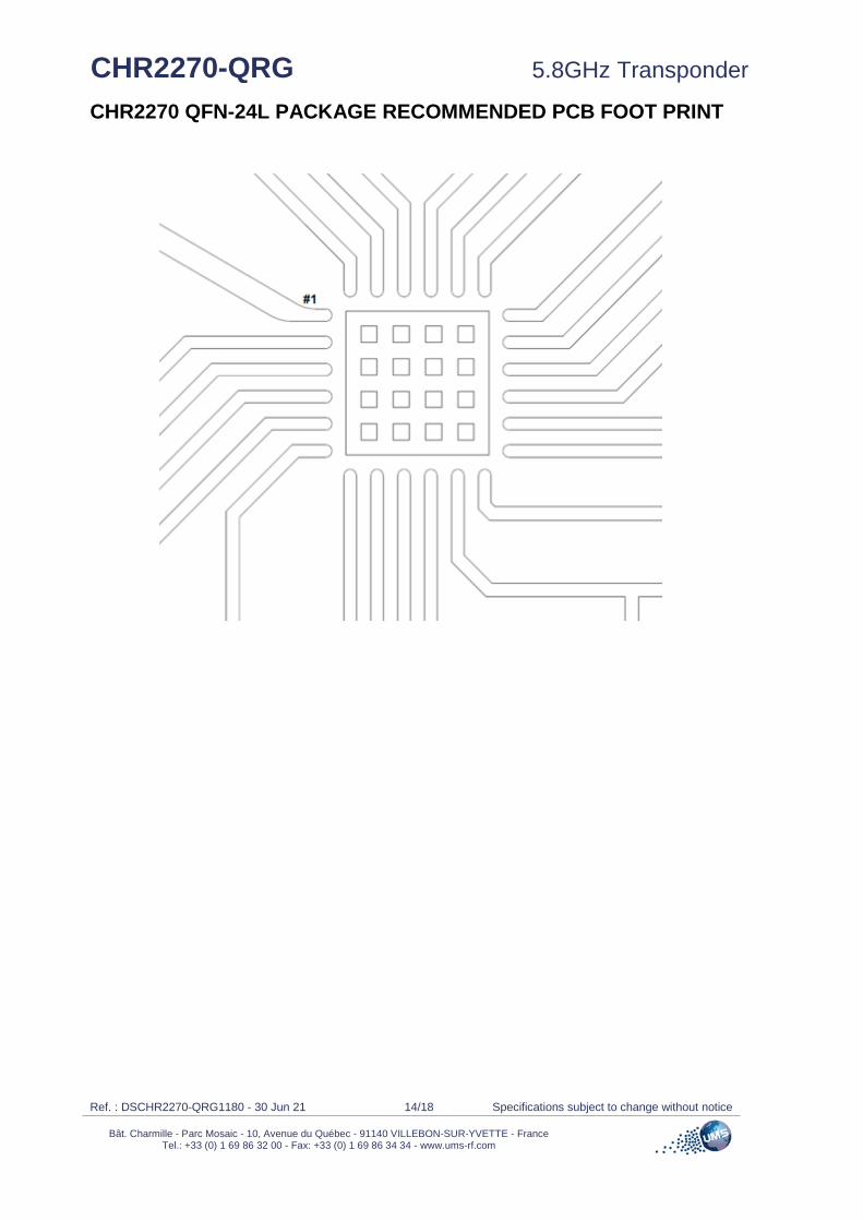
CHR2270 QFN-24L PACKAGE RECOMMENDED PCB FOOT PRINT

5.8GHz Transponder CHR2270-QRG
Ref. : DSCHR2270-QRG1180 - 30 Jun 21 15/18 Specifications subject to change without notice
Bât. Charmille - Parc Mosaic - 10, Avenue du Québec - 91140 VILLEBON-SUR-YVETTE - France Tel.: +33 (0) 1 69 86 32 00 - Fax: +33 (0) 1 69 86 34 34 - www.ums-rf.com
Evaluation mother board Compatible with the proposed footprint. Based on typically Ro4003 / 8mils or equivalent. Using a micro-strip to coplanar transition to access the package. Recommended for the implementation of this product on a module board. Decoupling capacitors of 10nF ±10% are recommended for all DC accesses. See application note AN0017 for details.
Note: All board measurements are performed using shielded cables, even for DC bias, to ensure safe operation.

CHR2270-QRG 5.8GHz Transponder
Ref. : DSCHR2270-QRG1180 - 30 Jun 21 16/18 Specifications subject to change without notice
Bât. Charmille - Parc Mosaic - 10, Avenue du Québec - 91140 VILLEBON-SUR-YVETTE - France Tel.: +33 (0) 1 69 86 32 00 - Fax: +33 (0) 1 69 86 34 34 - www.ums-rf.com
CHR2270 EXTERNAL COMPONENTS See “Specifications” and “ADJUSTMENT FEATURES” for appropriate values.

5.8GHz Transponder CHR2270-QRG
Ref. : DSCHR2270-QRG1180 - 30 Jun 21 17/18 Specifications subject to change without notice
Bât. Charmille - Parc Mosaic - 10, Avenue du Québec - 91140 VILLEBON-SUR-YVETTE - France Tel.: +33 (0) 1 69 86 32 00 - Fax: +33 (0) 1 69 86 34 34 - www.ums-rf.com
Notes

CHR2270-QRG 5.8GHz Transponder
Ref. : DSCHR2270-QRG1180 - 30 Jun 21 18/18 Specifications subject to change without notice
Bât. Charmille - Parc Mosaic - 10, Avenue du Québec - 91140 VILLEBON-SUR-YVETTE - France Tel.: +33 (0) 1 69 86 32 00 - Fax: +33 (0) 1 69 86 34 34 - www.ums-rf.com
Recommended package footprint Refer to the application note AN0017 available at https://www.ums-rf.com for package foot print recommendations. SMD mounting procedure For the mounting process standard techniques involving solder paste and a suitable reflow process can be used. For further details, see application note AN0017 at https://www.ums-rf.com. Recommended environmental management UMS products are compliant with the regulation in particular with the directives RoHS N°2011/65 and REACh N°1907/2006. More environmental data are available in the application note AN0019 also available at https://www.ums-rf.com. Recommended ESD management Refer to the application note AN0020 available at https://www.ums-rf.com for ESD sensitivity and handling recommendations for the UMS package products. Ordering Information QFN 4x4 package: CHR2270-QRG/XY Stick: XY = 20 Tape & reel: XY = 21 Information furnished is believed to be accurate and reliable. However United Monolithic Semiconductors S.A.S. assumes no responsibility for the consequences of use of such information nor for any infringement of patents or other rights of third parties which may result from its use. No license is granted by implication or otherwise under any patent or patent rights of United Monolithic Semiconductors S.A.S.. Specifications mentioned in this publication are subject to change without notice. This publication supersedes and replaces all information previously supplied. United Monolithic Semiconductors S.A.S. products are not authorised for use as critical components in life support devices or systems without express written approval from United Monolithic Semiconductors S.A.S.