Embed Size (px)
Citation preview
General DescriptionThe DS28E07 is a 1024-bit, 1-Wire® EEPROM chip orga-nized as four memory pages of 256 bits each. Data is written to an 8-byte scratchpad, verified, and then copied to the EEPROM memory. As a special feature, the four user memory pages can individually be write protected or put in EPROM-emulation mode, where bits can only be changed from a 1 to a 0 state. Each device has its own guaranteed unique 64-bit ROM identification number (ROM ID) that is factory programmed into the chip. The communication follows the 1-Wire protocol with the ROM ID acting as node address in the case of a multiple-device 1-Wire network.
Applications Accessory/PCB Identification Medical Sensor Calibration Data Storage Analog Sensor Calibration Including IEEE P1451.4
Smart Sensors Ink and Toner Print Cartridge Identification After-Market Management of Consumables
Benefits and Features Partitioning of Memory Provides Greater Flexibility in
Programming User Data• 1024 Bits of EEPROM Memory Organized as Four
Pages of 256 Bits• Individual Memory Pages Can Be Permanently
Write Protected or Put in EPROM-Emulation Mode (Write to 0)
Advanced 1-Wire Protocol Minimizes Interface to Just Single IO Reducing Required Pin Count and Enhancing Reliability• Unique Factory-Programmed, Unalterable 64-Bit
Identification Number• Switchpoint Hysteresis and Filtering to Optimize
Performance in the Presence of Noise• Communicates to Host with a Single Digital Signal
at 15.4kbps or 125kbps Using 1-Wire Protocol• Reads and Writes over a Wide Voltage Range from
3.0V to 5.25V from -40°C to +85°C• ±8kV HBM ESD Protection (typ) for IO Pin
Ordering Information appears at end of data sheet.
1-Wire is a registered trademark of Maxim Integrated Products, Inc.
19-7674; Rev 2; 1/17
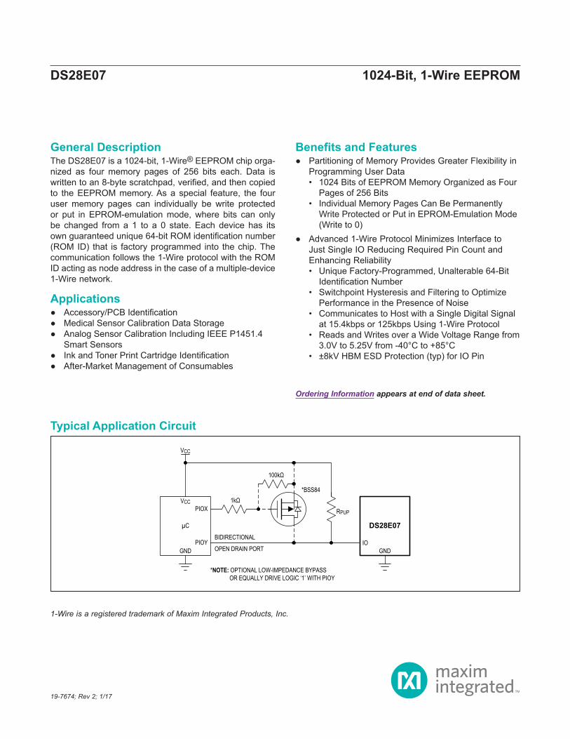
Typical Application Circuit
µC
PIOX
PIOY
100kΩ
DS28E07
RPUP
*BSS84
IO
*NOTE: OPTIONAL LOW-IMPEDANCE BYPASS OR EQUALLY DRIVE LOGIC ‘1’ WITH PIOY
BIDIRECTIONAL
GND
VCC
GND OPEN DRAIN PORT
1kΩ
VCC
DS28E07 1024-Bit, 1-Wire EEPROM
IO Voltage Range to GND .......................................-0.5V to +6VIO Sink Current.................................................................±10mAOperating Temperature Range ........................... -40°C to +85°CJunction Temperature ......................................................+150°C
Storage Temperature Range ............................ -55°C to +125°CLead Temperature (soldering, 10s) .................................+300°CLead Temperature (reflow) TO-92 ...................................+250°CLead Temperature (reflow) TDFN, TSOC........................+260°C
TSOC Junction-to-Ambient Thermal Resistance (θJA) ........127°C/W Junction-to-Case Thermal Resistance (θJC) ...............37°C/W
TO-92 Junction-to-Ambient Thermal Resistance (θJA) ........132°C/W Junction-to-Case Thermal Resistance (θJC) .................4°C/W
TDFN Junction-to-Ambient Thermal Resistance (θJA) ..........55°C/W Junction-to-Case Thermal Resistance (θJC) .................9°C/W
(Note 1)
(TA = -40°C to +85°C, unless otherwise noted.) (Note 2)
Note 1: Package thermal resistances were obtained using the method described in JEDEC specification JESD51-7, using a four-layer board. For detailed information on package thermal considerations, refer to www.maximintegrated.com/thermal-tutorial.
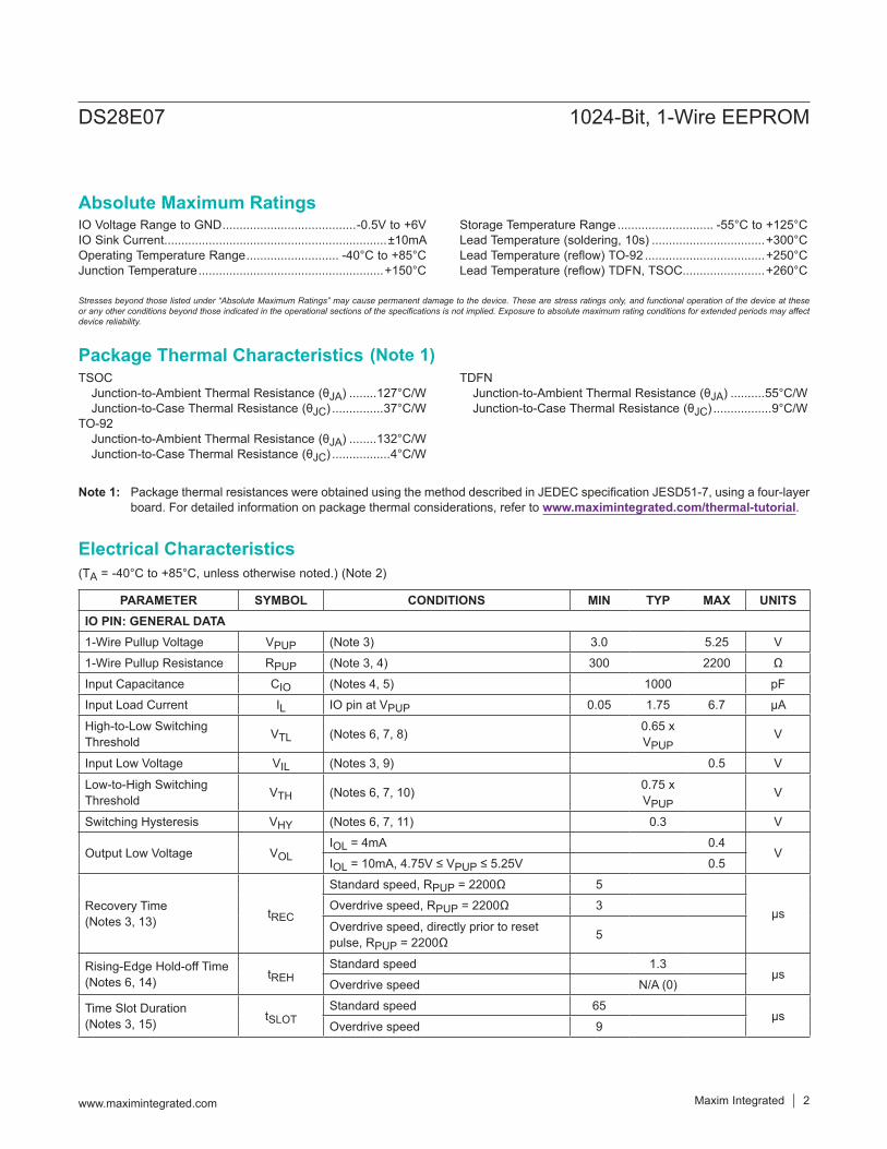
PARAMETER SYMBOL CONDITIONS MIN TYP MAX UNITSIO PIN: GENERAL DATA1-Wire Pullup Voltage VPUP (Note 3) 3.0 5.25 V
1-Wire Pullup Resistance RPUP (Note 3, 4) 300 2200 Ω
Input Capacitance CIO (Notes 4, 5) 1000 pF
Input Load Current IL IO pin at VPUP 0.05 1.75 6.7 µA
High-to-Low Switching Threshold VTL (Notes 6, 7, 8) 0.65 x
VPUPV
Input Low Voltage VIL (Notes 3, 9) 0.5 V
Low-to-High Switching Threshold VTH (Notes 6, 7, 10) 0.75 x
VPUPV
Switching Hysteresis VHY (Notes 6, 7, 11) 0.3 V
Output Low Voltage VOLIOL = 4mA 0.4
VIOL = 10mA, 4.75V ≤ VPUP ≤ 5.25V 0.5
Recovery Time(Notes 3, 13) tREC
Standard speed, RPUP = 2200Ω 5
µsOverdrive speed, RPUP = 2200Ω 3
Overdrive speed, directly prior to reset pulse, RPUP = 2200Ω 5
Rising-Edge Hold-off Time(Notes 6, 14) tREH
Standard speed 1.3µs
Overdrive speed N/A (0)
Time Slot Duration(Notes 3, 15) tSLOT
Standard speed 65µs
Overdrive speed 9
DS28E07 1024-Bit, 1-Wire EEPROM
www.maximintegrated.com Maxim Integrated 2
Absolute Maximum Ratings
Stresses beyond those listed under “Absolute Maximum Ratings” may cause permanent damage to the device. These are stress ratings only, and functional operation of the device at these or any other conditions beyond those indicated in the operational sections of the specifications is not implied. Exposure to absolute maximum rating conditions for extended periods may affect device reliability.
Package Thermal Characteristics
Electrical Characteristics
(TA = -40°C to +85°C, unless otherwise noted.) (Note 2)
Note 2: Limits are 100% production tested at TA = +25°C and TA = +85°C. Limits over the operating temperature range and relevant supply voltage range are guaranteed by design and characterization. Typical values are at TA = +25°C.
Note 3: System requirement.Note 4: Maximum allowable pullup resistance is a function of the number of 1-Wire devices in the system and 1-Wire recovery times.
The specified value here applies to systems with only one device and with the minimum 1-Wire recovery times.Note 5: Maximum value represents the internal parasite capacitance when VPUP is first applied. Once the parasite capacitance is
charged, it does not affect normal communication.Note 6: Guaranteed by design and/or characterization only. Not production tested.Note 7: VTL, VTH, and VHY are a function of the internal supply voltage, which is a function of VPUP, RPUP, 1-Wire timing, and
capacitive loading on IO. Lower VPUP, higher RPUP, shorter tREC, and heavier capacitive loading all lead to lower values of VTL, VTH, and VHY.
Note 8: Voltage below which, during a falling edge on IO, a logic-zero is detected.Note 9: The voltage on IO must be less than or equal to VILMAX at all times the master is driving IO to a logic-zero level.Note 10: Voltage above which, during a rising edge on IO, a logic-one is detected.Note 11: After VTH is crossed during a rising edge on IO, the voltage on IO must drop by at least VHY to be detected as logic-zero.
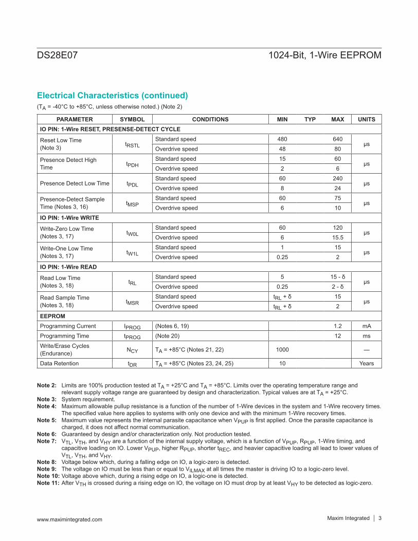
PARAMETER SYMBOL CONDITIONS MIN TYP MAX UNITSIO PIN: 1-Wire RESET, PRESENSE-DETECT CYCLE
Reset Low Time(Note 3) tRSTL
Standard speed 480 640µs
Overdrive speed 48 80
Presence Detect High Time tPDH
Standard speed 15 60µs
Overdrive speed 2 6
Presence Detect Low Time tPDLStandard speed 60 240
µsOverdrive speed 8 24
Presence-Detect Sample Time (Notes 3, 16) tMSP
Standard speed 60 75µs
Overdrive speed 6 10
IO PIN: 1-Wire WRITE
Write-Zero Low Time(Notes 3, 17) tW0L
Standard speed 60 120µs
Overdrive speed 6 15.5
Write-One Low Time(Notes 3, 17) tW1L
Standard speed 1 15µs
Overdrive speed 0.25 2
IO PIN: 1-Wire READ
Read Low Time(Notes 3, 18) tRL
Standard speed 5 15 - δµs
Overdrive speed 0.25 2 - δ
Read Sample Time(Notes 3, 18) tMSR
Standard speed tRL + δ 15µs
Overdrive speed tRL + δ 2
EEPROMProgramming Current IPROG (Notes 6, 19) 1.2 mA
Programming Time tPROG (Note 20) 12 ms
Write/Erase Cycles (Endurance) NCY TA = +85°C (Notes 21, 22) 1000 —
Data Retention tDR TA = +85°C (Notes 23, 24, 25) 10 Years
DS28E07 1024-Bit, 1-Wire EEPROM
www.maximintegrated.com Maxim Integrated 3
Electrical Characteristics (continued)
Note 13: Applies to a single device attached to a 1-Wire line.Note 14: The earliest recognition of a negative edge is possible at tREH after VTH has been previously reached. Note 15: Defines maximum possible bit rate. Equal to 1/(tW0LMIN + tRECMIN).Note 16: Interval after tRSTL during which a bus master can read a logic 0 on IO if there is a DS28E07 present. The power-up
presence detect pulse could be outside this interval but will be complete within 2ms after power-up.Note 17: ε in Figure 11 represents the time required for the pullup circuitry to pull the voltage on IO up from VIL to VTH. The actual
maximum duration for the master to pull the line low is tW1LMAX + tF - ε and tW0LMAX + tF - ε, respectively.Note 18: δ in Figure 11 represents the time required for the pullup circuitry to pull the voltage on IO up from VIL to the input-high
threshold of the bus master. The actual maximum duration for the master to pull the line low is tRLMAX + tF.Note 19: Current drawn from IO during the EEPROM programming interval. The pullup circuit on IO during the programming interval
should be such that the voltage at IO is greater than or equal to VPUPMIN. If VPUP in the system is close to VPUPMIN, a low impedance bypass of RPUP, which can be activated during programming, may need to be added.
Note 20: Interval begins tREHMAX after the trailing rising edge on IO for the last time slot of the E/S byte for a valid Copy Scratchpad sequence. Interval ends once the device’s self-timed EEPROM programming cycle is complete and the current drawn by the device has returned from IPROG to IL.
Note 21: Write-cycle endurance is tested in compliance with JESD47G.Note 22: Not 100% production tested; guaranteed by reliability monitor sampling.Note 23: Data retention is tested in compliance with JESD47G.Note 24: Guaranteed by 100% production test at elevated temperature for a shorter time; equivalence of this production test to the
data sheet limit at operating temperature range is established by reliability testing.Note 25: EEPROM writes can become nonfunctional after the data-retention time is exceeded. Long-term storage at elevated
temperatures is not recommended.
DS28E07 1024-Bit, 1-Wire EEPROM
www.maximintegrated.com Maxim Integrated 4
2
3
1
2
3
1
3
2
1
N.C.
IO
GND
TO-92
TOP VIEW
N.C.
IO
GND
N.C.
N.C.
N.C.
TSOC
+
5
4
6
2
3
1
DS28E07
FRONT VIEW (T&R VERSION)
FRONT VIEWSIDE VIEW
1 6N.C. N.C.
2 5IO N.C.
3 4GND N.C.
TDFN(3mm x 3mm)
TOP VIEW
2807ym
rrF
+
*EP
*EXPOSED PAD
DS28E07 1024-Bit, 1-Wire EEPROM
www.maximintegrated.com Maxim Integrated 5
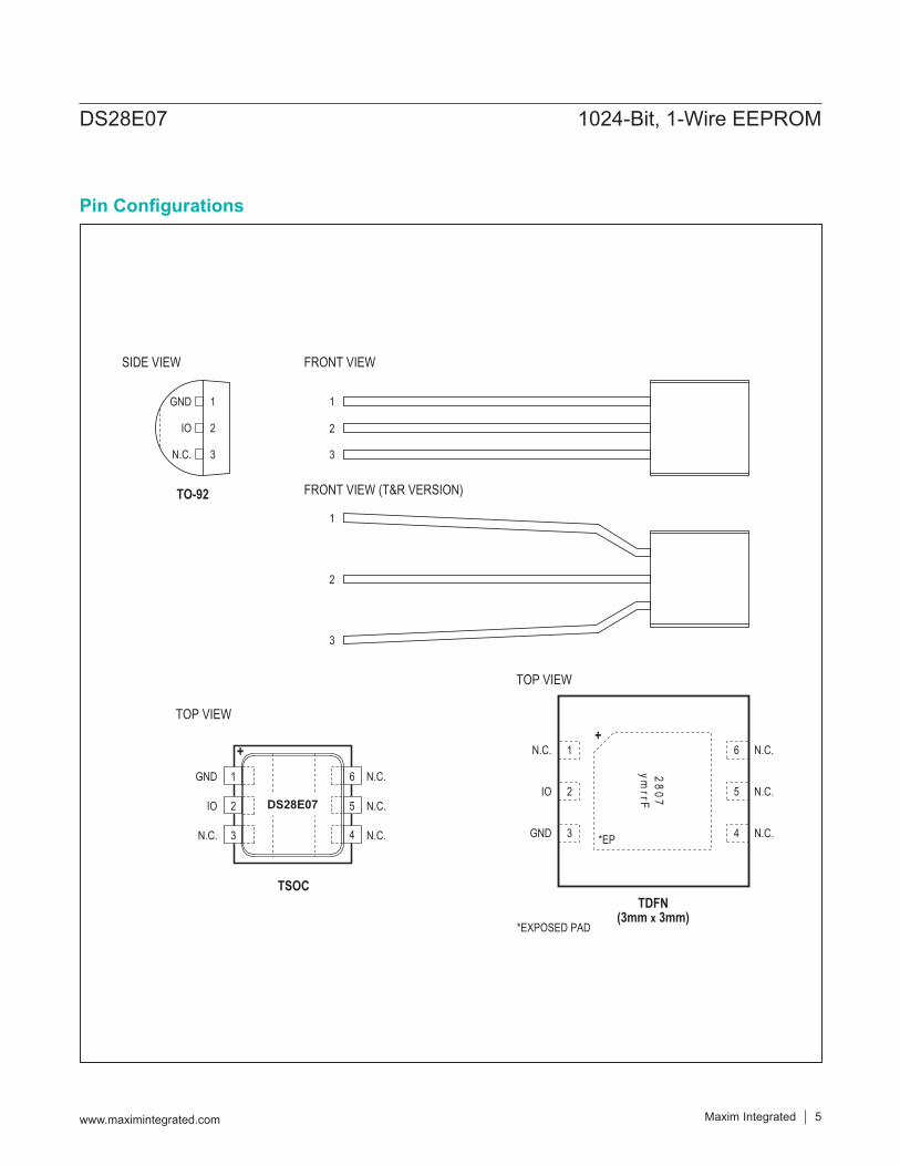
Pin Configurations
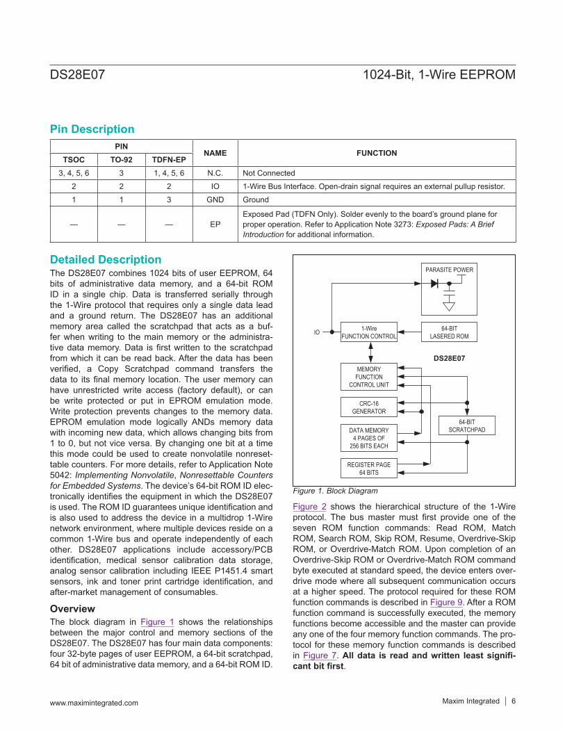
Detailed DescriptionThe DS28E07 combines 1024 bits of user EEPROM, 64 bits of administrative data memory, and a 64-bit ROM ID in a single chip. Data is transferred serially through the 1-Wire protocol that requires only a single data lead and a ground return. The DS28E07 has an additional memory area called the scratchpad that acts as a buf-fer when writing to the main memory or the administra-tive data memory. Data is first written to the scratchpad from which it can be read back. After the data has been verified, a Copy Scratchpad command transfers the data to its final memory location. The user memory can have unrestricted write access (factory default), or can be write protected or put in EPROM emulation mode. Write protection prevents changes to the memory data. EPROM emulation mode logically ANDs memory data with incoming new data, which allows changing bits from 1 to 0, but not vice versa. By changing one bit at a time this mode could be used to create nonvolatile nonreset-table counters. For more details, refer to Application Note 5042: Implementing Nonvolatile, Nonresettable Counters for Embedded Systems. The device’s 64-bit ROM ID elec-tronically identifies the equipment in which the DS28E07 is used. The ROM ID guarantees unique identification and is also used to address the device in a multidrop 1-Wire network environment, where multiple devices reside on a common 1-Wire bus and operate independently of each other. DS28E07 applications include accessory/PCB identification, medical sensor calibration data storage, analog sensor calibration including IEEE P1451.4 smart sensors, ink and toner print cartridge identification, and after-market management of consumables.
OverviewThe block diagram in Figure 1 shows the relationships between the major control and memory sections of the DS28E07. The DS28E07 has four main data components: four 32-byte pages of user EEPROM, a 64-bit scratchpad, 64 bit of administrative data memory, and a 64-bit ROM ID.
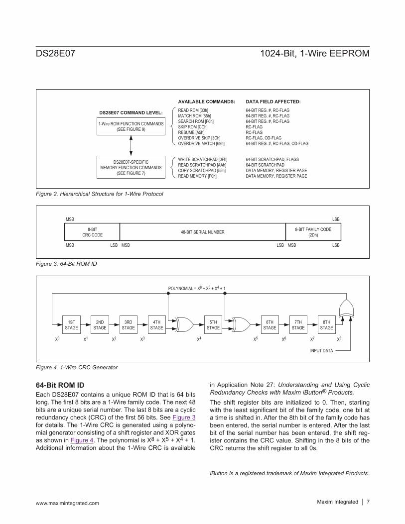
Figure 2 shows the hierarchical structure of the 1-Wire protocol. The bus master must first provide one of the seven ROM function commands: Read ROM, Match ROM, Search ROM, Skip ROM, Resume, Overdrive-Skip ROM, or Overdrive-Match ROM. Upon completion of an Overdrive-Skip ROM or Overdrive-Match ROM command byte executed at standard speed, the device enters over-drive mode where all subsequent communication occurs at a higher speed. The protocol required for these ROM function commands is described in Figure 9. After a ROM function command is successfully executed, the memory functions become accessible and the master can provide any one of the four memory function commands. The pro-tocol for these memory function commands is described in Figure 7. All data is read and written least signifi-cant bit first.
PINNAME FUNCTION
TSOC TO-92 TDFN-EP3, 4, 5, 6 3 1, 4, 5, 6 N.C. Not Connected
2 2 2 IO 1-Wire Bus Interface. Open-drain signal requires an external pullup resistor.
1 1 3 GND Ground
— — — EPExposed Pad (TDFN Only). Solder evenly to the board’s ground plane for proper operation. Refer to Application Note 3273: Exposed Pads: A Brief Introduction for additional information.
Figure 1. Block Diagram
MEMORYFUNCTION
CONTROL UNIT
DATA MEMORY4 PAGES OF
256 BITS EACH
CRC-16GENERATOR
64-BITSCRATCHPAD
1-WireFUNCTION CONTROL
64-BITLASERED ROM
PARASITE POWER
IO
REGISTER PAGE64 BITS
DS28E07
DS28E07 1024-Bit, 1-Wire EEPROM
www.maximintegrated.com Maxim Integrated 6
Pin Description
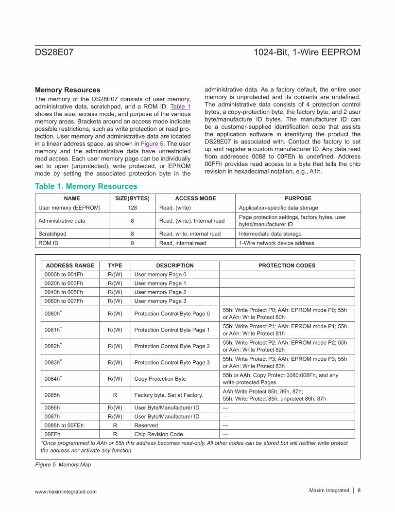
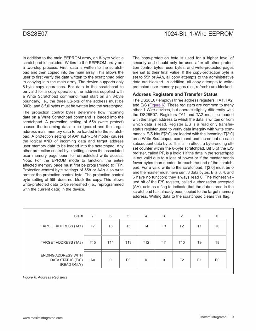
64-Bit ROM IDEach DS28E07 contains a unique ROM ID that is 64 bits long. The first 8 bits are a 1-Wire family code. The next 48 bits are a unique serial number. The last 8 bits are a cyclic redundancy check (CRC) of the first 56 bits. See Figure 3 for details. The 1-Wire CRC is generated using a polyno-mial generator consisting of a shift register and XOR gates as shown in Figure 4. The polynomial is X8 + X5 + X4 + 1. Additional information about the 1-Wire CRC is available
in Application Note 27: Understanding and Using Cyclic Redundancy Checks with Maxim iButton® Products.The shift register bits are initialized to 0. Then, starting with the least significant bit of the family code, one bit at a time is shifted in. After the 8th bit of the family code has been entered, the serial number is entered. After the last bit of the serial number has been entered, the shift reg-ister contains the CRC value. Shifting in the 8 bits of the CRC returns the shift register to all 0s.
Figure 2. Hierarchical Structure for 1-Wire Protocol
Figure 3. 64-Bit ROM ID
Figure 4. 1-Wire CRC Generator
DS28E07 COMMAND LEVEL:
AVAILABLE COMMANDS: DATA FIELD AFFECTED:
READ ROM [33h]MATCH ROM [55h]SEARCH ROM [F0h]SKIP ROM [CCh]RESUME [A5h]OVERDRIVE SKIP [3Ch]OVERDRIVE MATCH [69h]
64-BIT REG. #, RC-FLAG64-BIT REG. #, RC-FLAG64-BIT REG. #, RC-FLAGRC-FLAGRC-FLAGRC-FLAG, OD-FLAG64-BIT REG. #, RC-FLAG, OD-FLAG
1-Wire ROM FUNCTION COMMANDS(SEE FIGURE 9)
WRITE SCRATCHPAD [0Fh]READ SCRATCHPAD [AAh]COPY SCRATCHPAD [55h]READ MEMORY [F0h]
64-BIT SCRATCHPAD, FLAGS64-BIT SCRATCHPADDATA MEMORY, REGISTER PAGEDATA MEMORY, REGISTER PAGE
DS28E07-SPECIFICMEMORY FUNCTION COMMANDS
(SEE FIGURE 7)
MSB
8-BITCRC CODE 48-BIT SERIAL NUMBER
MSB MSBLSB
LSB
LSB
8-BIT FAMILY CODE(2Dh)
MSBLSB
1STSTAGE
2NDSTAGE
3RDSTAGE
4THSTAGE
7THSTAGE
8THSTAGE
6THSTAGE
5THSTAGE
X0 X1 X2 X3 X4
POLYNOMIAL = X8 + X5 + X4 + 1
INPUT DATA
X5 X6 X7 X8
DS28E07 1024-Bit, 1-Wire EEPROM
www.maximintegrated.com Maxim Integrated 7
iButton is a registered trademark of Maxim Integrated Products.
Memory ResourcesThe memory of the DS28E07 consists of user memory, administrative data, scratchpad, and a ROM ID. Table 1 shows the size, access mode, and purpose of the various memory areas. Brackets around an access mode indicate possible restrictions, such as write protection or read pro-tection. User memory and administrative data are located in a linear address space, as shown in Figure 5. The user memory and the administrative data have unrestricted read access. Each user memory page can be individually set to open (unprotected), write protected, or EPROM mode by setting the associated protection byte in the
administrative data. As a factory default, the entire user memory is unprotected and its contents are undefined. The administrative data consists of 4 protection control bytes, a copy-protection byte, the factory byte, and 2 user byte/manufacture ID bytes. The manufacturer ID can be a customer-supplied identification code that assists the application software in identifying the product the DS28E07 is associated with. Contact the factory to set up and register a custom manufacturer ID. Any data read from addresses 0088 to 00FEh is undefined. Address 00FFh provides read access to a byte that tells the chip revision in hexadecimal notation, e.g., A1h.
Table 1. Memory ResourcesNAME SIZE(BYTES) ACCESS MODE PURPOSE
User memory (EEPROM) 128 Read, (write) Application-specific data storage
Administrative data 8 Read, (write), Internal read Page protection settings, factory bytes, user bytes/manufacturer ID
Scratchpad 8 Read, write, internal read Intermediate data storage
ROM ID 8 Read, internal read 1-Wire network device address
Figure 5. Memory Map
ADDRESS RANGE TYPE DESCRIPTION PROTECTION CODES0000h to 001Fh R/(W) User memory Page 00020h to 003Fh R/(W) User memory Page 10040h to 005Fh R/(W) User memory Page 20060h to 007Fh R/(W) User memory Page 3
0080h* R/(W) Protection Control Byte Page 0 55h: Write Protect P0; AAh: EPROM mode P0; 55h or AAh: Write Protect 80h
0081h* R/(W) Protection Control Byte Page 1 55h: Write Protect P1; AAh: EPROM mode P1; 55h or AAh: Write Protect 81h
0082h* R/(W) Protection Control Byte Page 2 55h: Write Protect P2; AAh: EPROM mode P2; 55h or AAh: Write Protect 82h
0083h* R/(W) Protection Control Byte Page 3 55h: Write Protect P3; AAh: EPROM mode P3; 55h or AAh: Write Protect 83h
0084h* R/(W) Copy Protection Byte 55h or AAh: Copy Protect 0080:008Fh, and any write-protected Pages
0085h R Factory byte. Set at Factory. AAh:Write Protect 85h, 86h, 87h;55h: Write Protect 85h, unprotect 86h, 87h
0086h R/(W) User Byte/Manufacturer ID —0087h R/(W) User Byte/Manufacturer ID —0088h to 00FEh R Reserved —00FFh R Chip Revision Code —
*Once programmed to AAh or 55h this address becomes read-only. All other codes can be stored but will neither write protect the address nor activate any function.
DS28E07 1024-Bit, 1-Wire EEPROM
www.maximintegrated.com Maxim Integrated 8
In addition to the main EEPROM array, an 8-byte volatile scratchpad is included. Writes to the EEPROM array are a two-step process. First, data is written to the scratch-pad and then copied into the main array. This allows the user to first verify the data written to the scratchpad prior to copying into the main array. The device supports only 8-byte copy operations. For data in the scratchpad to be valid for a copy operation, the address supplied with a Write Scratchpad command must start on an 8-byte boundary, i.e., the three LS-bits of the address must be 000b, and 8 full bytes must be written into the scratchpad.The protection control bytes determine how incoming data on a Write Scratchpad command is loaded into the scratchpad. A protection setting of 55h (write protect) causes the incoming data to be ignored and the target address main memory data to be loaded into the scratch-pad. A protection setting of AAh (EPROM mode) causes the logical AND of incoming data and target address user memory data to be loaded into the scratchpad. Any other protection control byte setting leaves the associated user memory page open for unrestricted write access. Note: For the EPROM mode to function, the entire affected memory page must first be programmed to FFh. Protection-control byte settings of 55h or AAh also write protect the protection-control byte. The protection-control byte setting of 55h does not block the copy. This allows write-protected data to be refreshed (i.e., reprogrammed with the current data) in the device.
The copy-protection byte is used for a higher level of security and should only be used after all other protec-tion control bytes, user bytes, and write-protected pages are set to their final value. If the copy-protection byte is set to 55h or AAh, all copy attempts to the administrative data are blocked. In addition, all copy attempts to write-protected user memory pages (i.e., refresh) are blocked.
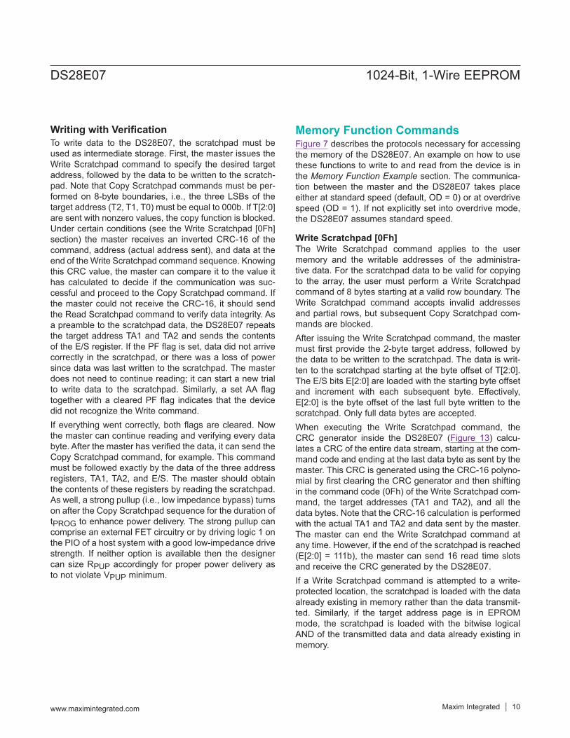
Address Registers and Transfer StatusThe DS28E07 employs three address registers: TA1, TA2, and E/S (Figure 6). These registers are common to many other 1-Wire devices, but operate slightly differently with the DS28E07. Registers TA1 and TA2 must be loaded with the target address to which the data is written or from which data is read. Register E/S is a read only transfer-status register used to verify data integrity with write com-mands. E/S bits E[2:0] are loaded with the incoming T[2:0] on a Write Scratchpad command and increment on each subsequent data byte. This is, in effect, a byte-ending off-set counter within the 8-byte scratchpad. Bit 5 of the E/S register, called PF, is a logic 1 if the data in the scratchpad is not valid due to a loss of power or if the master sends fewer bytes than needed to reach the end of the scratch-pad. For a valid write to the scratchpad, T[2:0] must be 0 and the master must have sent 8 data bytes. Bits 3, 4, and 6 have no function; they always read 0. The highest val-ued bit of the E/S register, called authorization accepted (AA), acts as a flag to indicate that the data stored in the scratchpad has already been copied to the target memory address. Writing data to the scratchpad clears this flag.
Figure 6. Address Registers
BIT # 7 6 5 4 3 2 1 0
TARGET ADDRESS (TA1) T7 T6 T5 T4 T3 T2 T1 T0
TARGET ADDRESS (TA2) T15 T14 T13 T12 T11 T10 T9 T8
ENDING ADDRESS WITHDATA STATUS (E/S)
(READ ONLY)AA 0 PF 0 0 E2 E1 E0
DS28E07 1024-Bit, 1-Wire EEPROM
www.maximintegrated.com Maxim Integrated 9
Writing with VerificationTo write data to the DS28E07, the scratchpad must be used as intermediate storage. First, the master issues the Write Scratchpad command to specify the desired target address, followed by the data to be written to the scratch-pad. Note that Copy Scratchpad commands must be per-formed on 8-byte boundaries, i.e., the three LSBs of the target address (T2, T1, T0) must be equal to 000b. If T[2:0] are sent with nonzero values, the copy function is blocked. Under certain conditions (see the Write Scratchpad [0Fh] section) the master receives an inverted CRC-16 of the command, address (actual address sent), and data at the end of the Write Scratchpad command sequence. Knowing this CRC value, the master can compare it to the value it has calculated to decide if the communication was suc-cessful and proceed to the Copy Scratchpad command. If the master could not receive the CRC-16, it should send the Read Scratchpad command to verify data integrity. As a preamble to the scratchpad data, the DS28E07 repeats the target address TA1 and TA2 and sends the contents of the E/S register. If the PF flag is set, data did not arrive correctly in the scratchpad, or there was a loss of power since data was last written to the scratchpad. The master does not need to continue reading; it can start a new trial to write data to the scratchpad. Similarly, a set AA flag together with a cleared PF flag indicates that the device did not recognize the Write command.If everything went correctly, both flags are cleared. Now the master can continue reading and verifying every data byte. After the master has verified the data, it can send the Copy Scratchpad command, for example. This command must be followed exactly by the data of the three address registers, TA1, TA2, and E/S. The master should obtain the contents of these registers by reading the scratchpad. As well, a strong pullup (i.e., low impedance bypass) turns on after the Copy Scratchpad sequence for the duration of tPROG to enhance power delivery. The strong pullup can comprise an external FET circuitry or by driving logic 1 on the PIO of a host system with a good low-impedance drive strength. If neither option is available then the designer can size RPUP accordingly for proper power delivery as to not violate VPUP minimum.
Memory Function CommandsFigure 7 describes the protocols necessary for accessing the memory of the DS28E07. An example on how to use these functions to write to and read from the device is in the Memory Function Example section. The communica-tion between the master and the DS28E07 takes place either at standard speed (default, OD = 0) or at overdrive speed (OD = 1). If not explicitly set into overdrive mode, the DS28E07 assumes standard speed.
Write Scratchpad [0Fh]The Write Scratchpad command applies to the user memory and the writable addresses of the administra-tive data. For the scratchpad data to be valid for copying to the array, the user must perform a Write Scratchpad command of 8 bytes starting at a valid row boundary. The Write Scratchpad command accepts invalid addresses and partial rows, but subsequent Copy Scratchpad com-mands are blocked.After issuing the Write Scratchpad command, the master must first provide the 2-byte target address, followed by the data to be written to the scratchpad. The data is writ-ten to the scratchpad starting at the byte offset of T[2:0]. The E/S bits E[2:0] are loaded with the starting byte offset and increment with each subsequent byte. Effectively, E[2:0] is the byte offset of the last full byte written to the scratchpad. Only full data bytes are accepted.When executing the Write Scratchpad command, the CRC generator inside the DS28E07 (Figure 13) calcu-lates a CRC of the entire data stream, starting at the com-mand code and ending at the last data byte as sent by the master. This CRC is generated using the CRC-16 polyno-mial by first clearing the CRC generator and then shifting in the command code (0Fh) of the Write Scratchpad com-mand, the target addresses (TA1 and TA2), and all the data bytes. Note that the CRC-16 calculation is performed with the actual TA1 and TA2 and data sent by the master. The master can end the Write Scratchpad command at any time. However, if the end of the scratchpad is reached (E[2:0] = 111b), the master can send 16 read time slots and receive the CRC generated by the DS28E07.If a Write Scratchpad command is attempted to a write-protected location, the scratchpad is loaded with the data already existing in memory rather than the data transmit-ted. Similarly, if the target address page is in EPROM mode, the scratchpad is loaded with the bitwise logical AND of the transmitted data and data already existing in memory.
DS28E07 1024-Bit, 1-Wire EEPROM
www.maximintegrated.com Maxim Integrated 10
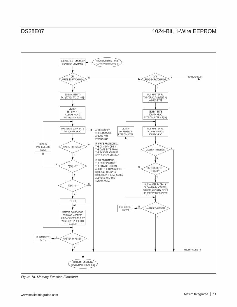
Figure 7a. Memory Function Flowchart
BUS MASTER Tx MEMORYFUNCTION COMMAND
BUS MASTER TxTA1 (T[7:0]), TA2 (T[15:8])
BUS MASTER RxTA1 (T[7:0]), TA2 (T[15:8]),
AND E/S BYTE
BUS MASTER RxDATA BYTE FROM
SCRATCHPAD
MASTER Tx DATA BYTETO SCRATCHPAD APPLIES ONLY
IF THE MEMORYAREA IS NOTPROTECTED.
IF WRITE PROTECTED,THE DS28E07 COPIESTHE DATE BYTE FROMTHE TARGET ADDRESSINTO THE SCRATCHPAD.
IF IN EPROM MODE,THE DS28E07 LOADSTHE BITWISE LOGICALAND OF THE TRANSMITTEDBYTE AND THE DATABYTE FROM THE TARGETEDADDRESS INTO THESCRATCHPAD.
BUS MASTERRx "1"s
DS28E07INCREMENTS
E[2:0]
PF = 0
DS28E07SETS PF = 1
CLEARS AA = 0SETS E[2:0] = T[2:0]
0FhWRITE SCRATCHPAD?
N
Y
N
Y
N
Y
Y
Y
N
N
MASTER Tx RESET?
E[2:0] = 7?
T[2:0] = 0?
MASTER Tx RESET?
DS28E07 SETSSCRATCHPAD
BYTE COUNTER = T[2:0]
AAhREAD SCRATCHPAD?
N
Y
DS28E07 Tx CRC-16 OFCOMMAND, ADDRESS,
AND DATA BYTES AS THEYWERE SENT BY THE BUS
MASTER
BUS MASTERRx "1"s
Y
NMASTER Tx RESET?
BUS MASTER Rx CRC-16OF COMMAND, ADDRESS,
E/S BYTE, AND DATA BYTESAS SENT BY THE DS28E07
Y
N
MASTER Tx RESET?
Y
BYTE COUNTER= E[2:0]?
FROM ROM FUNCTIONSFLOWCHART (FIGURE 9)
TO ROM FUNCTIONSFLOWCHART (FIGURE 9)
DS28E07INCREMENTS
BYTE COUNTER
N
TO FIGURE 7b
FROM FIGURE 7b
DS28E07 1024-Bit, 1-Wire EEPROM
www.maximintegrated.com Maxim Integrated 11
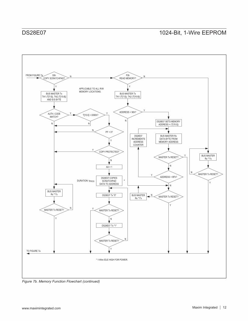
Figure 7b. Memory Function Flowchart (continued)
BUS MASTER TxTA1 (T[7:0]), TA2 (T[15:8])
APPLICABLE TO ALL R/WMEMORY LOCATIONS.
DURATION: tPROG *
* 1-Wire IDLE HIGH FOR POWER.
DS28E07 COPIESSCRATCHPAD
DATA TO ADDRESS
BUS MASTERRx "1"s
AA = 1
BUS MASTERRx "1"s
MASTER Tx RESET?N Y
N
N
MASTER Tx RESET?
Y
MASTER Tx RESET?
BUS MASTER TxTA1 (T[7:0]), TA2 (T[15:8])
AND E/S BYTE
55hCOPY SCRATCHPAD?
N
Y
Y
Y
N
DS28E07 Tx "0"
DS28E07 Tx "1"
F0hREAD MEMORY?
N
Y
Y
N
AUTH. CODEMATCH?
Y
N
Y
N
N
T[15:0] < 0090h?
PF = 0?
ADDRESS < 90h?
YCOPY PROTECTED?
BUS MASTERRx "1"s
MASTER Tx RESET?N
Y
DS28E07 SETS MEMORYADDRESS = (T[15:0])
BUS MASTER RxDATA BYTE FROM
MEMORY ADDRESS
Y
N
N
MASTER Tx RESET?
ADDRESS < 8Fh?
N
Y
MASTER Tx RESET?
DS28E07INCREMENTS
ADDRESSCOUNTER
Y
TO FIGURE 7a
FROM FIGURE 7a
DS28E07 1024-Bit, 1-Wire EEPROM
www.maximintegrated.com Maxim Integrated 12
Read Scratchpad [AAh]The Read Scratchpad command allows verifying the tar-get address and the integrity of the scratchpad data. After issuing the command code, the master begins reading. The first two bytes are the target address. The next byte is the ending offset/data status byte (E/S) followed by the scratchpad data, which may be different from what the master originally sent. This is of particular importance if the target address is within the administrative data sec-tion or a page in either write-protection mode or EPROM mode. See the Write Scratchpad [0Fh] section for details. The master should read through the scratchpad (E[2:0] - T[2:0] + 1 bytes), after which it receives the inverted CRC based on data as it was sent by the DS28E07. If the mas-ter continues reading after the CRC, all data is logic 1.
Copy Scratchpad [55h]The Copy Scratchpad command is used to copy data from the scratchpad to writable memory sections. After issuing the Copy Scratchpad command, the master must provide a 3-byte authorization pattern, which should have been obtained by an immediately preceding Read Scratchpad command. This 3-byte pattern must exactly match the data contained in the three address registers (TA1, TA2, E/S, in that order). If the pattern matches, the target address is valid, the PF flag is not set, and the tar-get memory is not copy protected, then the AA flag is set and the copy begins. All 8 bytes of scratchpad contents are copied to the target memory location. The duration of the device’s internal data transfer is tPROG during which the voltage on the 1-Wire bus must not fall below VPUP minimum. Best practice is to generate a strong pullup that turns on after the Copy Scratchpad sequence for the duration of tPROG to enhance power delivery. A pattern of
alternating 0s and 1s are transmitted after the data has been copied until the master issues a reset pulse. If the PF flag is set or the target memory is copy protected, the copy does not begin and the AA flag is not set.
Read Memory [F0h]The Read Memory command is the general function to read data from the DS28E07. After issuing the command, the master must provide the 2-byte target address. After these 2 bytes, the master reads data beginning from the target address and can continue until address 00FFh. If the master continues reading, the result is logic 1s. The device’s internal TA1, TA2, E/S, and scratchpad contents are not affected by a Read Memory command.
1-Wire Bus SystemThe 1-Wire bus is a system that has a single bus master and one or more slaves. In all instances, the DS28E07 is a slave device. The bus master is typically a microcon-troller. The discussion of this bus system is broken down into three topics: hardware configuration, transaction sequence, and 1-Wire signaling (signal types and timing). The 1-Wire protocol defines bus transactions in terms of the bus state during specific time slots, which are initiated on the falling edge of sync pulses from the bus master.
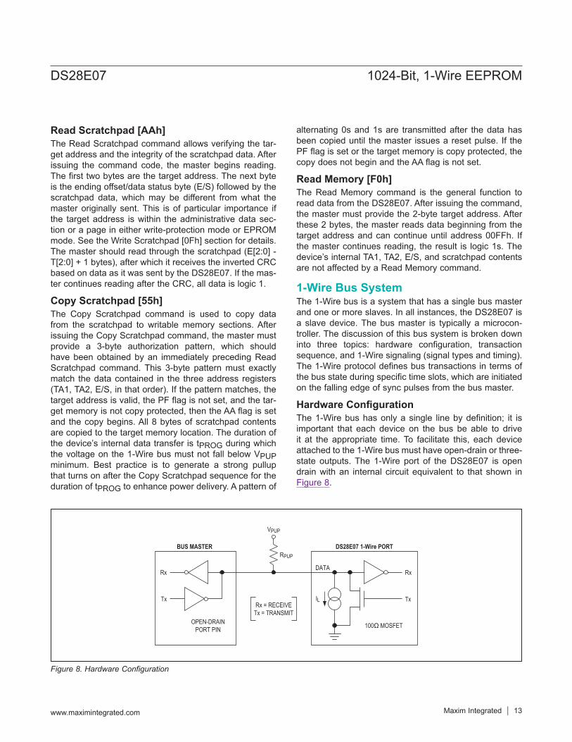
Hardware ConfigurationThe 1-Wire bus has only a single line by definition; it is important that each device on the bus be able to drive it at the appropriate time. To facilitate this, each device attached to the 1-Wire bus must have open-drain or three-state outputs. The 1-Wire port of the DS28E07 is open drain with an internal circuit equivalent to that shown in Figure 8.
Figure 8. Hardware Configuration
Rx
RPUP
IL
VPUP
BUS MASTER
OPEN-DRAINPORT PIN 100Ω MOSFET
Tx
Rx
Tx
DATA
DS28E07 1-Wire PORT
Rx = RECEIVETx = TRANSMIT
DS28E07 1024-Bit, 1-Wire EEPROM
www.maximintegrated.com Maxim Integrated 13
A multidrop bus consists of a 1-Wire bus with multiple slaves attached. The DS28E07 supports both a standard and overdrive communication speed of 15.4kbps (max) and 125kbps (max), respectively. The value of the pullup resistor primarily depends on the network size and load conditions. The DS28E07 requires a pullup resistor of 2.2kΩ (max) at any speed.The idle state for the 1-Wire bus is high. If for any reason a transaction needs to be suspended, the bus must be left in the idle state if the transaction is to resume. If this does not occur and the bus is left low for more than 15.5μs (overdrive speed) or more than 120μs (standard speed), one or more devices on the bus could be reset.
Transaction SequenceThe protocol for accessing the DS28E07 through the 1-Wire port is as follows:
Initialization ROM function command Memory function command Transaction/data
InitializationAll transactions on the 1-Wire bus begin with an initializa-tion sequence. The initialization sequence consists of a reset pulse transmitted by the bus master followed by presence pulse(s) transmitted by the slave(s). The pres-ence pulse lets the bus master know that the DS28E07 is on the bus and is ready to operate. For more details, see the 1-Wire Signaling section.
1-Wire ROM Function CommandsOnce the bus master has detected a presence, it can issue one of the seven ROM function commands that the DS28E07 supports. All ROM function commands are 8 bits long. A list of these commands follows. See Figure 9.
Read ROM [33h]The Read ROM command allows the bus master to read the DS28E07’s 8-bit family code, unique 48-bit serial number, and 8-bit CRC. This command can only be used if there is a single slave on the bus. If more than one slave is present on the bus, a data collision occurs when all slaves try to transmit at the same time (open drain
produces a wired-AND result). The resultant family code and 48-bit serial number result in a mismatch of the CRC.
Match ROM [55h]The Match ROM command, followed by a 64-bit ROM sequence, allows the bus master to address a specific DS28E07 on a multidrop bus. Only the DS28E07 that exactly matches the 64-bit ROM sequence responds to the subsequent memory function command. All other slaves wait for a reset pulse. This command can be used with a single device or multiple devices on the bus.
Search ROM [F0h]When a system is initially brought up, the bus master might not know the number of devices on the 1-Wire bus or their ROM ID numbers. By taking advantage of the wired-AND property of the bus, the master can use a pro-cess of elimination to identify the ID of all slave devices. For each bit in the ID number, starting with the least sig-nificant bit, the bus master issues a triplet of time slots. On the first slot, each slave device participating in the search outputs the true value of its ID number bit. On the second slot, each slave device participating in the search outputs the complemented value of its ID number bit. On the third slot, the master writes the true value of the bit to be selected. All slave devices that do not match the bit written by the master stop participating in the search. If both of the read bits are zero, the master knows that slave devices exist with both states of the bit. By choos-ing which state to write, the bus master branches in the search tree. After one complete pass, the bus master knows the ROM ID number of a single device. Additional passes identify the ID numbers of the remaining devices. Refer to Application Note 187: 1-Wire Search Algorithm for a detailed discussion, including an example.
Skip ROM [CCh]This command can save time in a single-drop bus sys-tem by allowing the bus master to access the memory functions without providing the 64-bit ROM ID. If more than one slave is present on the bus and, for example, a read command is issued following the Skip ROM com-mand, data collision occurs on the bus as multiple slaves transmit simultaneously (open-drain pulldowns produce a wired-AND result).
DS28E07 1024-Bit, 1-Wire EEPROM
www.maximintegrated.com Maxim Integrated 14
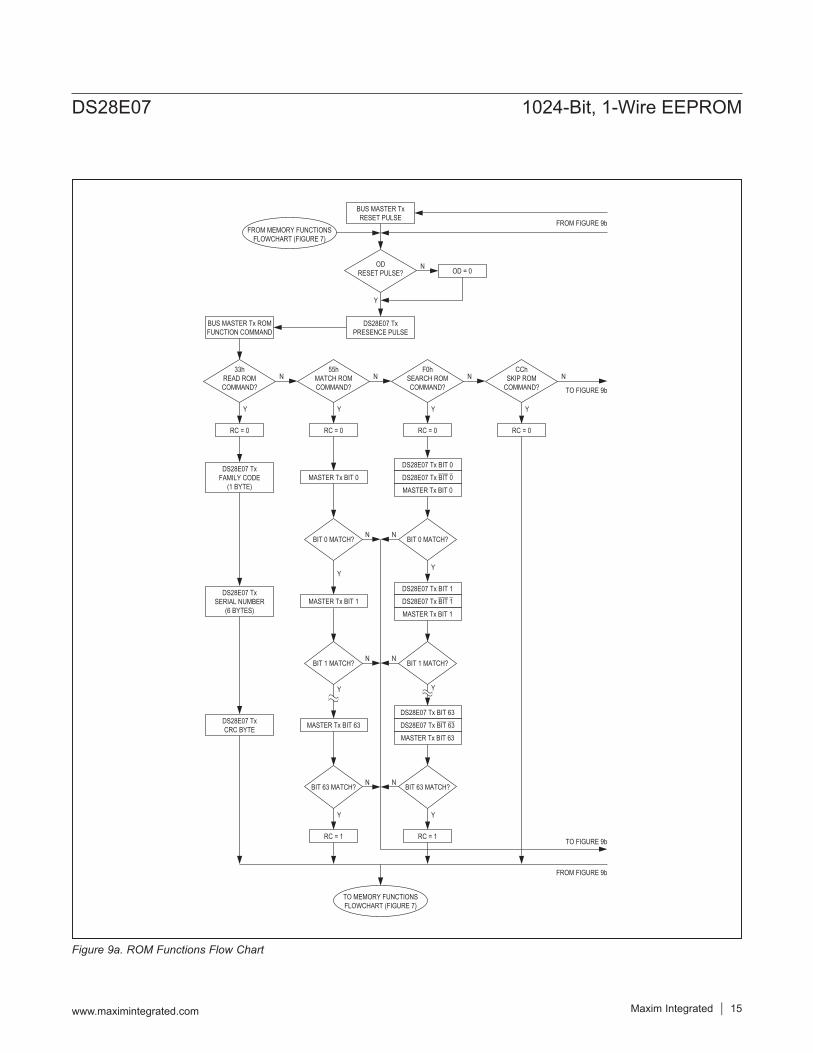
Figure 9a. ROM Functions Flow Chart
DS28E07 TxPRESENCE PULSE
BUS MASTER TxRESET PULSE
BUS MASTER Tx ROMFUNCTION COMMAND
DS28E07 TxCRC BYTE
DS28E07 TxFAMILY CODE
(1 BYTE)
DS28E07 TxSERIAL NUMBER
(6 BYTES)
RC = 0
MASTER Tx BIT 0
RC = 0 RC = 0 RC = 0
OD = 0
YY
Y
Y
Y
Y
Y
Y
33hREAD ROMCOMMAND?
N55h
MATCH ROMCOMMAND?
BIT 0 MATCH? BIT 0 MATCH?
N
N N
N N
N N
F0hSEARCH ROMCOMMAND?
ODRESET PULSE?
N
N
CChSKIP ROM
COMMAND?N
RC = 1
MASTER Tx BIT 1
MASTER Tx BIT 63
BIT 1 MATCH?
BIT 63 MATCH?
Y
Y
RC = 1
FROM MEMORY FUNCTIONSFLOWCHART (FIGURE 7)
TO MEMORY FUNCTIONSFLOWCHART (FIGURE 7)
DS28E07 Tx BIT 0DS28E07 Tx BIT 0MASTER Tx BIT 0
BIT 1 MATCH?
BIT 63 MATCH?
DS28E07 Tx BIT 1DS28E07 Tx BIT 1MASTER Tx BIT 1
DS28E07 Tx BIT 63DS28E07 Tx BIT 63MASTER Tx BIT 63
Y
TO FIGURE 9b
TO FIGURE 9b
FROM FIGURE 9b
FROM FIGURE 9b
DS28E07 1024-Bit, 1-Wire EEPROM
www.maximintegrated.com Maxim Integrated 15
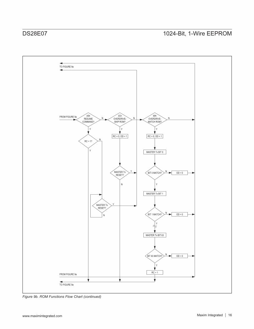
Figure 9b. ROM Functions Flow Chart (continued)
RC = 0; OD = 1 RC = 0; OD = 1
N
BIT 0 MATCH?
YN
RC = 1?
Y
A5hRESUME
COMMAND?N
Y
3ChOVERDRIVE-SKIP ROM?
N
Y
69hOVERDRIVE-MATCH ROM?
FROM FIGURE 9a
FROM FIGURE 9a
TO FIGURE 9a
TO FIGURE 9a
N
Y
Y
N
MASTER TxRESET?
YMASTER TxRESET?
N BIT 1 MATCH?
MASTER Tx BIT 0
MASTER Tx BIT 1
OD = 0
N OD = 0
N OD = 0
Y
RC = 1
BIT 63 MATCH?
MASTER Tx BIT 63
Y
DS28E07 1024-Bit, 1-Wire EEPROM
www.maximintegrated.com Maxim Integrated 16
Resume [A5h]To maximize the data throughput in a multidrop environ-ment, the Resume command is available. This command checks the status of the RC bit and, if it is set, directly transfers control to the memory function commands, similar to a Skip ROM command. The only way to set the RC bit is through successfully executing the Match ROM, Search ROM, or Overdrive-Match ROM command. Once the RC bit is set, the device can repeatedly be accessed through the Resume command. Accessing another device on the bus clears the RC bit, preventing two or more devices from simultaneously responding to the Resume command.
Overdrive-Skip ROM [3Ch]On a single-drop bus this command can save time by allowing the bus master to access the memory functions without providing the 64-bit ROM ID. Unlike the normal Skip ROM command, the Overdrive-Skip ROM command sets the DS28E07 into the overdrive mode (OD = 1). All communication following this command must occur at overdrive speed until a reset pulse of minimum 480μs duration resets all devices on the bus to standard speed (OD = 0).When issued on a multidrop bus, this command sets all overdrive-supporting devices into overdrive mode. To subsequently address a specific overdrive-supporting device, a reset pulse at overdrive speed must be issued followed by a Match ROM or Search ROM command sequence. This speeds up the time for the search pro-cess. If more than one slave supporting overdrive is pres-ent on the bus and the Overdrive-Skip ROM command is followed by a read command, data collision occurs on the bus as multiple slaves transmit simultaneously (open-drain pulldowns produce a wired-AND result).
Overdrive-Match ROM [69h]The Overdrive-Match ROM command followed by a 64-bit ROM sequence transmitted at overdrive speed allows the bus master to address a specific DS28E07 on a multi-drop bus and to simultaneously set it in overdrive mode. Only the DS28E07 that exactly matches the 64-bit ROM sequence responds to the subsequent memory function command. Slaves already in overdrive mode from a previ-ous Overdrive-Skip ROM or successful Overdrive-Match ROM command remain in overdrive mode. All overdrive-capable slaves return to standard speed at the next reset pulse of minimum 480μs duration. The Overdrive-Match ROM command can be used with a single device or mul-tiple devices on the bus.
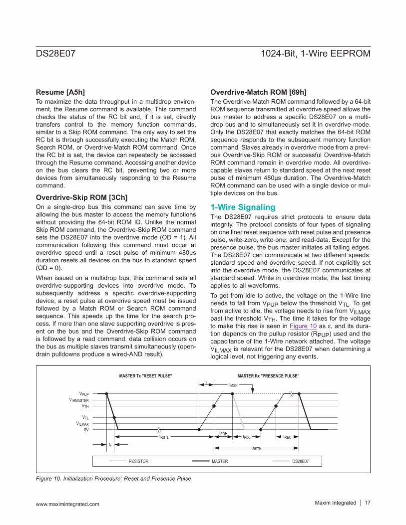
1-Wire SignalingThe DS28E07 requires strict protocols to ensure data integrity. The protocol consists of four types of signaling on one line: reset sequence with reset pulse and presence pulse, write-zero, write-one, and read-data. Except for the presence pulse, the bus master initiates all falling edges. The DS28E07 can communicate at two different speeds: standard speed and overdrive speed. If not explicitly set into the overdrive mode, the DS28E07 communicates at standard speed. While in overdrive mode, the fast timing applies to all waveforms.To get from idle to active, the voltage on the 1-Wire line needs to fall from VPUP below the threshold VTL. To get from active to idle, the voltage needs to rise from VILMAX past the threshold VTH. The time it takes for the voltage to make this rise is seen in Figure 10 as ε, and its dura-tion depends on the pullup resistor (RPUP) used and the capacitance of the 1-Wire network attached. The voltage VILMAX is relevant for the DS28E07 when determining a logical level, not triggering any events.
Figure 10. Initialization Procedure: Reset and Presence Pulse
RESISTOR MASTER DS28E07
tRSTL tPDL
tRSTH
tPDH
MASTER Tx "RESET PULSE" MASTER Rx "PRESENCE PULSE"
VPUPVIHMASTER
VTH
VTLVILMAX
0V
ε
tF
tREC
tMSP
DS28E07 1024-Bit, 1-Wire EEPROM
www.maximintegrated.com Maxim Integrated 17
Figure 10 shows the initialization sequence required to begin any communication with the DS28E07. A reset pulse followed by a presence pulse indicates that the DS28E07 is ready to receive data, given the correct ROM and memory function command. If the bus master uses slew-rate control on the falling edge, it must pull down the line for tRSTL + tF to compensate for the edge. A tRSTL dura-tion of 480μs or longer exits the overdrive mode, returning the device to standard speed. If the DS28E07 is in over-drive mode and tRSTL is no longer than 80μs, the device remains in overdrive mode. If the device is in overdrive mode and tRSTL is between 80μs and 480μs, the device resets, but the communication speed is undetermined.After the bus master has released the line it goes into receive mode. Now the 1-Wire bus is pulled to VPUP through the pullup resistor or, in the case of a special driver chip, through the active circuitry. When the thresh-old VTH is crossed, the DS28E07 waits for tPDH and then transmits a presence pulse by pulling the line low for tPDL. To detect a presence pulse, the master must test the logi-cal state of the 1-Wire line at tMSP.The tRSTH window must be at least the sum of tPDH-MAX, tPDLMAX, and tRECMIN. Immediately after tRSTH is expired, the DS28E07 is ready for data communication. In a mixed population network, tRSTH should be extended to minimum 480μs at standard speed and 48μs at overdrive speed to accommodate other 1-Wire devices.
Read/Write Time SlotsData communication with the DS28E07 takes place in time slots that carry a single bit each. Write time slots transport data from bus master to slave. Read time slots transfer data from slave to master. Figure 11 illustrates the definitions of the write and read time slots. All communication begins with the master pulling the data line low. As the voltage on the 1-Wire line falls below the threshold VTL, the DS28E07 starts its internal timing generator that determines when the data line is sampled during a write time slot and how long data is valid during a read time slot.
Master-to-SlaveFor a write-one time slot, the voltage on the data line must have crossed the VTH threshold before the write-one low time tW1LMAX is expired. For a write-zero time slot, the voltage on the data line must stay below the VTH threshold until the write-zero low time tW0LMIN is expired. For the most reliable communication, the voltage on the data line should not exceed VILMAX during the entire tW0L or tW1L window. After the VTH threshold has been crossed, the DS28E07 needs a recovery time tREC before it is ready for the next time slot.
Slave-to-MasterA read-data time slot begins like a write-one time slot. The voltage on the data line must remain below VTL until the read low time tRL is expired. During the tRL window, when responding with a 0, the DS28E07 starts pulling the data line low; its internal timing generator determines when this pulldown ends and the voltage starts rising again. When responding with a 1, the DS28E07 does not hold the data line low at all, and the voltage starts rising as soon as tRL is over.The sum of tRL + δ (rise time) on one side and the internal timing generator of the DS28E07 on the other side define the master sampling window (tMSRMIN to tMSRMAX), in which the master must perform a read from the data line. For the most reliable communication, tRL should be as short as permissible, and the master should read close to but no later than tMSRMAX. After reading from the data line, the master must wait until tSLOT is expired. This guarantees sufficient recovery time tREC for the DS28E07 to get ready for the next time slot. Note that tREC speci-fied herein applies only to a single DS28E07 attached to a 1-Wire line. For multidevice configurations, tREC must be extended to accommodate the additional 1-Wire device input capacitance. Alternatively, an interface that performs active pullup during the 1-Wire recovery time such as the special 1-Wire line drivers can be used.
DS28E07 1024-Bit, 1-Wire EEPROM
www.maximintegrated.com Maxim Integrated 18
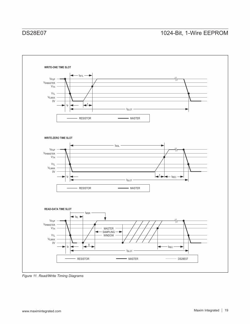
Figure 11. Read/Write Timing Diagrams
RESISTOR MASTER
RESISTOR MASTER
RESISTOR MASTER DS28E07
ε
ε
δ
VPUPVIHMASTER
VTH
VTLVILMAX
0VtF
VPUPVIHMASTER
VTH
VTLVILMAX
0VtF
VPUPVIHMASTER
VTH
VTLVILMAX
0VtF
tSLOT
tW1L
tRECtSLOT
tSLOT
tW0L
tREC
MASTERSAMPLINGWINDOW
tRL
tMSR
WRITE-ONE TIME SLOT
WRITE-ZERO TIME SLOT
READ-DATA TIME SLOT
DS28E07 1024-Bit, 1-Wire EEPROM
www.maximintegrated.com Maxim Integrated 19
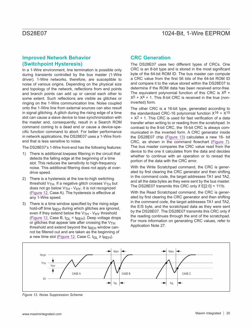
Improved Network Behavior (Switchpoint Hysteresis)In a 1-Wire environment, line termination is possible only during transients controlled by the bus master (1-Wire driver). 1-Wire networks, therefore, are susceptible to noise of various origins. Depending on the physical size and topology of the network, reflections from end points and branch points can add up or cancel each other to some extent. Such reflections are visible as glitches or ringing on the 1-Wire communication line. Noise coupled onto the 1-Wire line from external sources can also result in signal glitching. A glitch during the rising edge of a time slot can cause a slave device to lose synchronization with the master and, consequently, result in a Search ROM command coming to a dead end or cause a device-spe-cific function command to abort. For better performance in network applications, the DS28E07 uses a 1-Wire front-end that is less sensitive to noise.The DS28E07’s 1-Wire front-end has the following features:1) There is additional lowpass filtering in the circuit that
detects the falling edge at the beginning of a time slot. This reduces the sensitivity to high-frequency noise. This additional filtering does not apply at over-drive speed.
2) There is a hysteresis at the low-to-high switching threshold VTH. If a negative glitch crosses VTH but does not go below VTH - VHY, it is not recognized (Figure 12, Case A). The hysteresis is effective at any 1-Wire speed.
3) There is a time window specified by the rising edge hold-off time tREH during which glitches are ignored, even if they extend below the VTH - VHY threshold (Figure 12, Case B, tGL < tREH). Deep voltage drops or glitches that appear late after crossing the VTH threshold and extend beyond the tREH window can-not be filtered out and are taken as the beginning of a new time slot (Figure 12, Case C, tGL ≥ tREH).
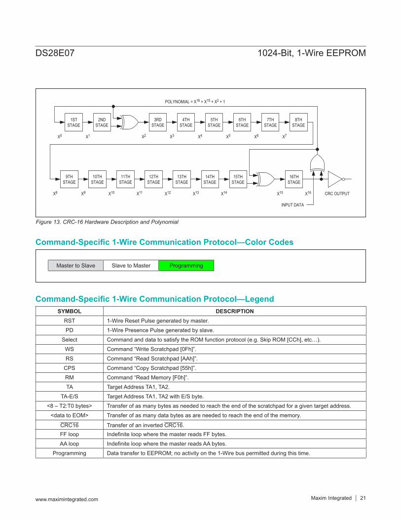
CRC GenerationThe DS28E07 uses two different types of CRCs. One CRC is an 8-bit type and is stored in the most significant byte of the 64-bit ROM ID. The bus master can compute a CRC value from the first 56 bits of the 64-bit ROM ID and compare it to the value stored within the DS28E07 to determine if the ROM data has been received error-free. The equivalent polynomial function of this CRC is X8 + X5 + X4 + 1. This 8-bit CRC is received in the true (non-inverted) form.The other CRC is a 16-bit type, generated according to the standardized CRC-16 polynomial function X16 + X15 + X2 + 1. This CRC is used for fast verification of a data transfer when writing to or reading from the scratchpad. In contrast to the 8-bit CRC, the 16-bit CRC is always com-municated in the inverted form. A CRC generator inside the DS28E07 chip (Figure 13) calculates a new 16- bit CRC, as shown in the command flowchart (Figure 7). The bus master compares the CRC value read from the device to the one it calculates from the data and decides whether to continue with an operation or to reread the portion of the data with the CRC error.With the Write Scratchpad command, the CRC is gener-ated by first clearing the CRC generator and then shifting in the command code, the target addresses TA1 and TA2, and all the data bytes as they were sent by the bus master. The DS28E07 transmits this CRC only if E[2:0] = 111b.With the Read Scratchpad command, the CRC is gener-ated by first clearing the CRC generator and then shifting in the command code, the target addresses TA1 and TA2, the E/S byte, and the scratchpad data as they were sent by the DS28E07. The DS28E07 transmits this CRC only if the reading continues through the end of the scratchpad. For more information on generating CRC values, refer to Application Note 27.
Figure 12. Noise Suppression Scheme
VPUP
VTHVHY
0V
tREH
tGL
tREH
tGL
CASE A CASE CCASE B
DS28E07 1024-Bit, 1-Wire EEPROM
www.maximintegrated.com Maxim Integrated 20
SYMBOL DESCRIPTIONRST 1-Wire Reset Pulse generated by master.
PD 1-Wire Presence Pulse generated by slave.
Select Command and data to satisfy the ROM function protocol (e.g. Skip ROM [CCh], etc…).
WS Command “Write Scratchpad [0Fh]”.
RS Command “Read Scratchpad [AAh]”.
CPS Command “Copy Scratchpad [55h]”.
RM Command “Read Memory [F0h]”.
TA Target Address TA1, TA2.
TA-E/S Target Address TA1, TA2 with E/S byte.
<8 – T2:T0 bytes> Transfer of as many bytes as needed to reach the end of the scratchpad for a given target address.
<data to EOM> Transfer of as many data bytes as are needed to reach the end of the memory.
CRC16 Transfer of an inverted CRC16.FF loop Indefinite loop where the master reads FF bytes.
AA loop Indefinite loop where the master reads AA bytes.
Programming Data transfer to EEPROM; no activity on the 1-Wire bus permitted during this time.
Figure 13. CRC-16 Hardware Description and Polynomial
1STSTAGE
2NDSTAGE
3RDSTAGE
4THSTAGE
7THSTAGE
8THSTAGE
6THSTAGE
5THSTAGE
X0 X1 X2 X3 X4
POLYNOMIAL = X16 + X15 + X2 + 1
INPUT DATA
CRC OUTPUT
X5 X6
11THSTAGE
12THSTAGE
15THSTAGE
14THSTAGE
13THSTAGE
X11 X12
9THSTAGE
10THSTAGE
X9 X10 X13 X14
X7
16THSTAGE
X16X15X8
Master to Slave Slave to Master Programming
DS28E07 1024-Bit, 1-Wire EEPROM
www.maximintegrated.com Maxim Integrated 21
Command-Specific 1-Wire Communication Protocol—Color Codes
Command-Specific 1-Wire Communication Protocol—Legend
+Denotes a lead-free/RoHS-compliant package.T = Tape and reel.*EP = Exposed pad.
PART TEMP RANGE PIN-PACKAGEDS28E07+ -40°C to +85°C 3 TO-92
DS28E07+T -40°C to +85°C 3 TO-92 (2k pcs)
DS28E07P+ -40°C to +85°C 6 TSOC
DS28E07P+T -40°C to +85°C 6 TSOC (4k pcs)
DS28E07Q+T -40°C to +85°C 6 TDFN-EP* (2.5k pcs)
PACKAGE TYPE
PACKAGE CODE
OUTLINENO.
LANDPATTERN NO.
3 TO-92(Bulk) Q3+1 21-0248 —
3 TO-92(T&R) Q3+4 21-0250 —
6 TSOC D6+1 21-0382 90-03216 TDFN-EP T633+2 21-0137 90-0058
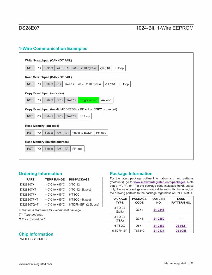
Write Scratchpad (CANNOT FAIL)
RST PD Select WS TA <8 – T2:T0 bytes> CRC16 FF loop
Read Scratchpad (CANNOT FAIL)
RST PD Select RS TA-E/S <8 – T2:T0 bytes> CRC16 FF loop
Copy Scratchpad (success)
RST PD Select CPS TA-E/S Programming AA loop
Copy Scratchpad (invalid ADDRESS or PF = 1 or COPY protected)
RST PD Select CPS TA-E/S FF loop
Read Memory (success)
RST PD Select RM TA <data to EOM> FF loop
Read Memory (invalid address)
RST PD Select RM TA FF loop
DS28E07 1024-Bit, 1-Wire EEPROM
www.maximintegrated.com Maxim Integrated 22
1-Wire Communication Examples
Chip InformationPROCESS: CMOS
Ordering Information Package InformationFor the latest package outline information and land patterns (footprints), go to www.maximintegrated.com/packages. Note that a “+”, “#”, or “-” in the package code indicates RoHS status only. Package drawings may show a different suffix character, but the drawing pertains to the package regardless of RoHS status.
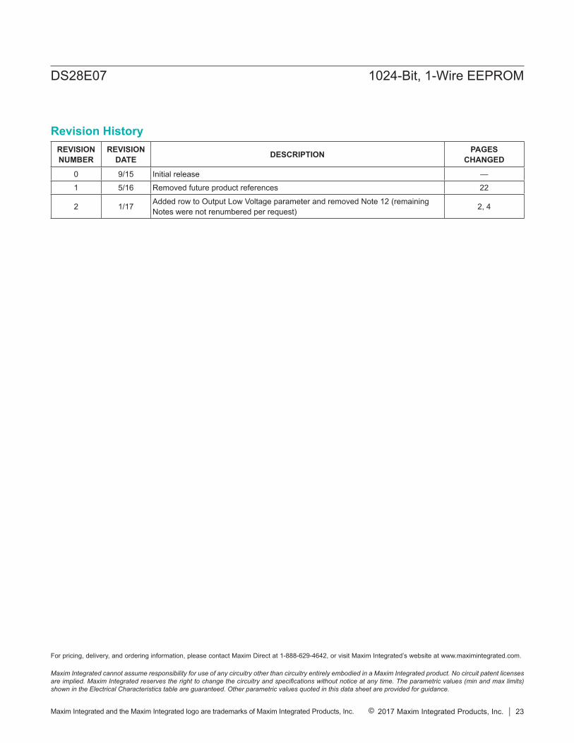
REVISIONNUMBER
REVISIONDATE DESCRIPTION PAGES
CHANGED
0 9/15 Initial release —
1 5/16 Removed future product references 22
2 1/17 Added row to Output Low Voltage parameter and removed Note 12 (remaining Notes were not renumbered per request) 2, 4
Maxim Integrated cannot assume responsibility for use of any circuitry other than circuitry entirely embodied in a Maxim Integrated product. No circuit patent licenses are implied. Maxim Integrated reserves the right to change the circuitry and specifications without notice at any time. The parametric values (min and max limits) shown in the Electrical Characteristics table are guaranteed. Other parametric values quoted in this data sheet are provided for guidance.
Maxim Integrated and the Maxim Integrated logo are trademarks of Maxim Integrated Products, Inc. © 2017 Maxim Integrated Products, Inc. 23
DS28E07 1024-Bit, 1-Wire EEPROM
Revision History
For pricing, delivery, and ordering information, please contact Maxim Direct at 1-888-629-4642, or visit Maxim Integrated’s website at www.maximintegrated.com.