Embed Size (px)
Citation preview
1 of 38 080202
Note: Some revisions of this device may incorporate deviations from published specifications known as errata. Multiple revisions of any devicemay be simultaneously available through various sales channels. For information about device errata, click here: http://www.maxim-ic.com/errata.
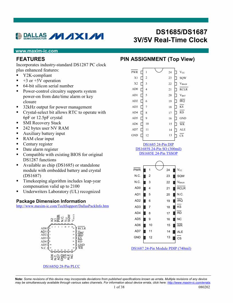
FEATURESIncorporates industry-standard DS1287 PC clockplus enhanced features:� Y2K-compliant� +3 or +5V operation� 64-bit silicon serial number� Power-control circuitry supports system
power-on from date/time alarm or keyclosure
� 32kHz output for power management� Crystal-select bit allows RTC to operate with
6pF or 12.5pF crystal� SMI Recovery Stack� 242 bytes user NV RAM� Auxiliary battery input� RAM clear input� Century register� Date alarm register� Compatible with existing BIOS for original
DS1287 functions� Available as chip (DS1685) or standalone
module with embedded battery and crystal(DS1687)
PIN ASSIGNMENT (Top View)
� Timekeeping algorithm includes leap-yearcompensation valid up to 2100
� Underwriters Laboratory (UL) recognized
Package Dimension Informationhttp://www.maxim-ic.com/TechSupport/DallasPackInfo.htm
1
2
3
4
5
6
7
8
9
10
24
23
22
21
20
19
18
17
16
15
VCC
SQW
VBAUX
RCLR
N.C.
IRQ
KS
RD
NC
WR
PWR
N.C.
N.C.
AD0
AD1
AD2
AD3
AD4
AD5
AD6
DS1687 24-Pin Module PDIP (740mil)
11
12
14
13
AD7
GND
ALE
CS
1
2
3
4
5
6
7
8
9
10
24
23
22
21
20
19
18
17
16
15
VCC
SQW
VBAUX
RCLR
VBAT
IRQ
KS
RD
GND
WR
PWR
X1
X2
AD0
AD1
AD2
AD3
AD4
AD5
AD6
DS1685 24-Pin DIPDS1685S 24-Pin SO (300mil)
DS1685E 24-Pin TSSOP
11
12
14
13
AD7
GND
ALE
CS
X2 X1 PWR
N.C
.V C
CSQ
W
DS1685Q 28-Pin PLCC
AD0AD1AD2AD3AD4AD5
RCLRVBATIRQKSRDGND
N.C. WR
AD6
N.C
.AD
7G
ND CS
ALE
NC
25
24
23
22
21
20
19
5
6
7
8
9
10
11
4 3 2 1 28 27 26
12 13 14 15 16 17 18
VB
AU
X
DS1685/DS16873V/5V Real-Time Clock
www.maxim-ic.com
www.maxim-ic.com
DS1685/DS1687
2 of 38
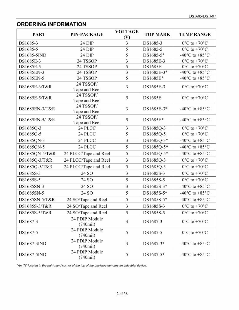
ORDERING INFORMATION
PART PIN-PACKAGE VOLTAGE(V) TOP MARK TEMP RANGE
DS1685-3 24 DIP 3 DS1685-3 0°C to +70°CDS1685-5 24 DIP 5 DS1685-5 0°C to +70°CDS1685-5IND 24 DIP 5 DS1685-5* -40°C to +85°CDS1685E-3 24 TSSOP 3 DS1685E-3 0°C to +70°CDS1685E-5 24 TSSOP 5 DS1685E 0°C to +70°CDS1685EN-3 24 TSSOP 3 DS1685E-3* -40°C to +85°CDS1685EN-5 24 TSSOP 5 DS1685E* -40°C to +85°C
DS1685E-3/T&R 24 TSSOP/Tape and Reel 3 DS1685E-3 0°C to +70°C
DS1685E-5/T&R 24 TSSOP/Tape and Reel 5 DS1685E 0°C to +70°C
DS1685EN-3/T&R 24 TSSOP/Tape and Reel 3 DS1685E-3* -40°C to +85°C
DS1685EN-5/T&R 24 TSSOP/Tape and Reel 5 DS1685E* -40°C to +85°C
DS1685Q-3 24 PLCC 3 DS1685Q-3 0°C to +70°CDS1685Q-5 24 PLCC 5 DS1685Q-5 0°C to +70°CDS1685QN-3 24 PLCC 3 DS1685Q-3* -40°C to +85°CDS1685QN-5 24 PLCC 5 DS1685Q-5* -40°C to +85°CDS1685QN-5/T&R 24 PLCC/Tape and Reel 5 DS1685Q-5* -40°C to +85°CDS1685Q-3/T&R 24 PLCC/Tape and Reel 3 DS1685Q-3 0°C to +70°CDS1685Q-5/T&R 24 PLCC/Tape and Reel 5 DS1685Q-5 0°C to +70°CDS1685S-3 24 SO 3 DS1685S-3 0°C to +70°CDS1685S-5 24 SO 5 DS1685S-5 0°C to +70°CDS1685SN-3 24 SO 3 DS1685S-3* -40°C to +85°CDS1685SN-5 24 SO 5 DS1685S-5* -40°C to +85°CDS1685SN-5/T&R 24 SO/Tape and Reel 5 DS1685S-5* -40°C to +85°CDS1685S-3/T&R 24 SO/Tape and Reel 3 DS1685S-3 0°C to +70°CDS1685S-5/T&R 24 SO/Tape and Reel 5 DS1685S-5 0°C to +70°C
DS1687-3 24 PDIP Module(740mil) 3 DS1687-3 0°C to +70°C
DS1687-5 24 PDIP Module(740mil) 5 DS1687-5 0°C to +70°C
DS1687-3IND 24 PDIP Module(740mil) 3 DS1687-3* -40°C to +85°C
DS1687-5IND 24 PDIP Module(740mil) 5 DS1687-5* -40°C to +85°C
*An “N” located in the right-hand corner of the top of the package denotes an industrial device.
DS1685/DS1687
3 of 38
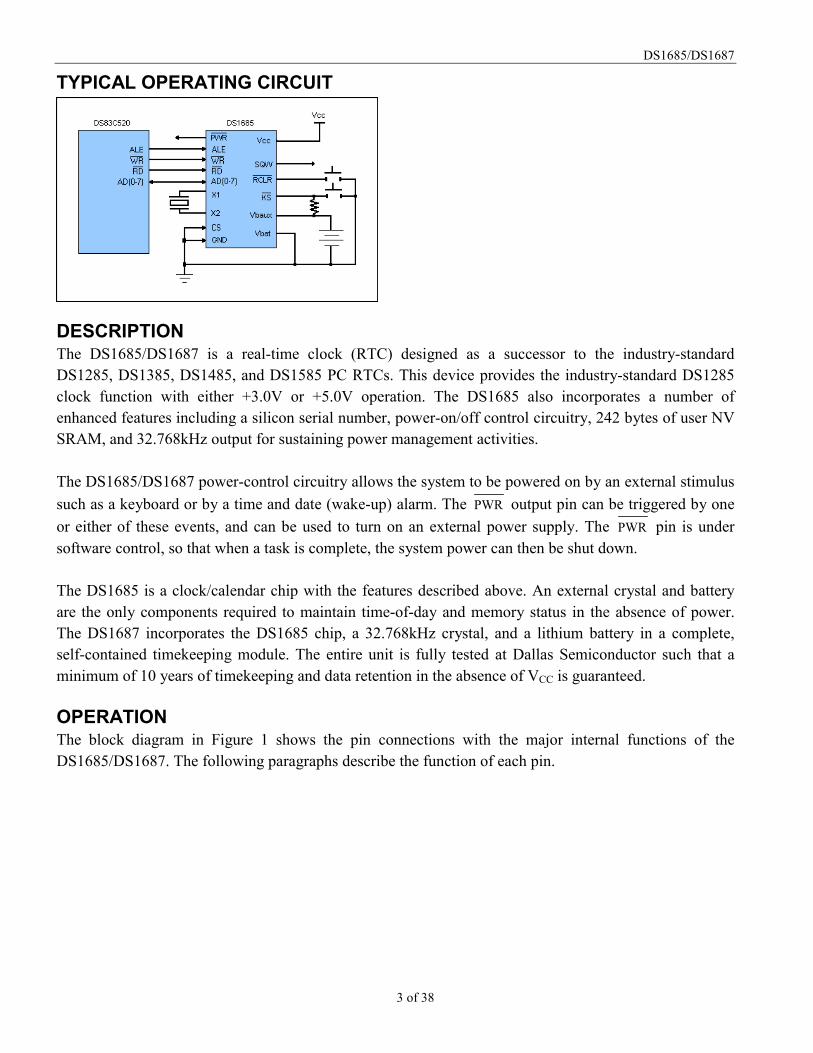
TYPICAL OPERATING CIRCUIT
DESCRIPTIONThe DS1685/DS1687 is a real-time clock (RTC) designed as a successor to the industry-standardDS1285, DS1385, DS1485, and DS1585 PC RTCs. This device provides the industry-standard DS1285clock function with either +3.0V or +5.0V operation. The DS1685 also incorporates a number ofenhanced features including a silicon serial number, power-on/off control circuitry, 242 bytes of user NVSRAM, and 32.768kHz output for sustaining power management activities.
The DS1685/DS1687 power-control circuitry allows the system to be powered on by an external stimulussuch as a keyboard or by a time and date (wake-up) alarm. The PWR output pin can be triggered by oneor either of these events, and can be used to turn on an external power supply. The PWR pin is undersoftware control, so that when a task is complete, the system power can then be shut down.
The DS1685 is a clock/calendar chip with the features described above. An external crystal and batteryare the only components required to maintain time-of-day and memory status in the absence of power.The DS1687 incorporates the DS1685 chip, a 32.768kHz crystal, and a lithium battery in a complete,self-contained timekeeping module. The entire unit is fully tested at Dallas Semiconductor such that aminimum of 10 years of timekeeping and data retention in the absence of VCC is guaranteed.
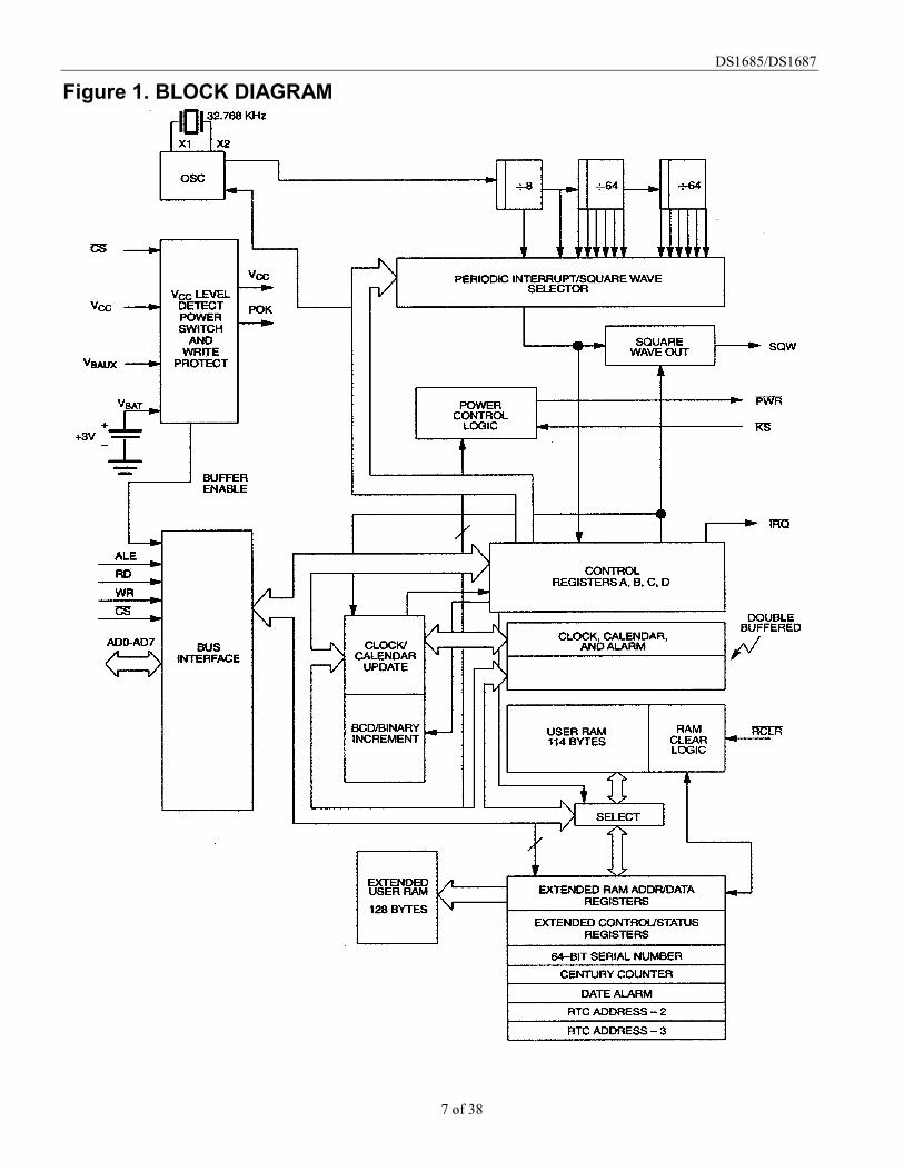
OPERATIONThe block diagram in Figure 1 shows the pin connections with the major internal functions of theDS1685/DS1687. The following paragraphs describe the function of each pin.
DS1685/DS1687
4 of 38
SIGNAL DESCRIPTIONS
GND, VCC – DC power is provided to the device on these pins. VCC is the +3V or +5V input.
SQW (Square-Wave Output) - The SQW pin provides a 32kHz square-wave output, tREC, after a power-up condition has been detected. This condition sets the following bits, enabling the 32kHz output;DV1 = 1, and E32K = 1. A square wave is output on this pin if either SQWE = 1 or E32K = 1. If E32K =1, then 32kHz is output regardless of the other control bits. If E32K = 0, then the output frequency isdependent on the control bits in register A. The SQW pin can output a signal from one of 13 tapsprovided by the 15 internal divider stages of the RTC. The frequency of the SQW pin can be changed byprogramming Register A as shown in Table 2. The SQW signal can be turned on and off using the SQWEbit in register B or the E32K bit in extended register 4Bh. A 32kHz SQW signal is output when theenable-32kHz (E32K) bit in extended register 4Bh is a logic 1 and VCC is above VPF. A 32kHz squarewave is also available when VCC is less than VPF if E32K = 1, ABE = 1, and voltage is applied to theVBAUX pin.
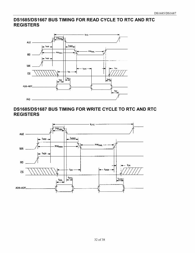
AD0–AD7 (Multiplexed Bidirectional Address/Data Bus) – Multiplexed buses save pins becauseaddress information and data information time-share the same signal paths. The addresses are presentduring the first portion of the bus cycle and the same pins and signal paths are used for data in the secondportion of the cycle. Address/data multiplexing does not slow the access time of the DS1685 since the buschange from address to data occurs during the internal RAM access time. Addresses must be valid priorto the latter portion of ALE, at which time the DS1685/DS1687 latches the address. Valid write data mustbe present and held stable during the latter portion of the WR pulse. In a read cycle, the DS1685/DS1687outputs 8 bits of data during the latter portion of the RD pulse. The read cycle is terminated and the busreturns to a high-impedance state as RD transitions high. The address/data bus also serves as abidirectional data path for the external extended RAM.
ALE (RTC Address-Strobe Input; Active High) – A pulse on the address strobe pin serves todemultiplex the bus. The falling edge of ALE causes the RTC address to be latched within theDS1685/DS1687.
RD (RTC Read Input; Active Low) - RD identifies the time period when the DS1685/DS1687 drivesthe bus with RTC read data. The RD signal is an enable signal for the output buffers of the clock.
WR (RTC Write Input; Active Low) -The WR signal is an active-low signal. The WR signal definesthe time period during which data is written to the addressed register.
CS (RTC Chip-Select Input; Active Low) – The chip-select signal must be asserted low during a buscycle for the RTC portion of the DS1685/DS1687 to be accessed. CS must be kept in the active stateduring RD and WR timing. Bus cycles that take place with ALE asserted but without asserting CS latchaddresses. However, no data transfer occurs.
IRQ (Interrupt-Request Output; Open Drain, Active Low) – The IRQ pin is an active-low output ofthe DS1685/DS1687 that can be connected to the interrupt input of a processor. The IRQ output remainslow as long as the status bit causing the interrupt is present and the corresponding interrupt-enable bit is
DS1685/DS1687
5 of 38
set. To clear the IRQ pin, the application software must clear all enabled flag bits contributing to IRQ ’sactive state.
When no interrupt conditions are present, the IRQ level is in the high-impedance state. Multipleinterrupting devices can be connected to an IRQ bus. The IRQ pin is an open-drain output and requires anexternal pullup resistor. The voltage on the pullup supply should be no greater than VCC + 0.2V.
PWR (Power-On Output; Open Drain, Active Low) – The PWR pin is intended for use as an on/offcontrol for the system power. With VCC voltage removed from the DS1685/DS1687, PWR can beautomatically activated from a kickstart input by the KS pin or from a wake-up interrupt. Once thesystem is powered on, the state of PWR can be controlled by bits in the Dallas registers. The PWR pincan be connected through a pullup resistor to a positive supply. For 5V operation, the voltage of thepullup supply should be no greater than 5.7V. For 3V operation, the voltage of the pullup supply shouldbe no greater than 3.9V.
KS (Kickstart Input; Active Low) – When VCC is removed from the DS1685/DS1687, the system canbe powered on in response to an active-low transition on the KS pin, as might be generated from a keyclosure. VBAUX must be present and the auxiliary-battery enable bit (ABE) must be set to 1 if the kickstartfunction is used, and the KS pin must be pulled up to the VBAUX supply. While VCC is applied, the KS pincan be used as an interrupt input.
RCLR (RAM Clear Input; Active Low) – If enabled by software, taking RCLR low clears the 242bytes of user RAM. When enabled, RCLR can be activated whether or not VCC is present. The RCLRfunction is designed to be used by a human interface (shorting to ground manually or by a switch) and notto be driven with external buffers. This pin is internally pulled up. Do not use an external pullup resistoron this pin.
VBAUX – Auxiliary battery input required for kickstart and wake-up features. This input also supportsclock/ calendar and user RAM if VBAT is at lower voltage or is not present. A standard +3V lithium cell orother energy source can be used. Battery voltage must be held between +2.5V and +3.7V for properoperation. If VBAUX is not going to be used it should be grounded, and auxiliary-battery enable bit bank 1,register 4BH, should equal 0.
See “Conditions of Acceptability” at http://www.maxim-ic.com/TechSupport/QA/ntrl.htm.
DS1685 ONLY
X1, X2 – Connections for a standard 32.768kHz quartz crystal. For greatest accuracy, the DS1685 mustbe used with a crystal that has a specified load capacitance of either 6pF or 12.5pF. The crystal-select(CS) bit in Extended Control Register 4B is used to select operation with a 6pF or 12.5pF crystal. Thecrystal is attached directly to the X1 and X2 pins. There is no need for external capacitors or resistors.Note: X1 and X2 are very high-impedance nodes. It is recommended that they and the crystal be guard-ringed with ground and that high-frequency signals be kept away from the crystal area.

DS1685/DS1687
6 of 38
VBAT – Battery input for any standard 3V lithium cell or other energy source. Battery voltage must beheld between 2.5V and 3.7V for proper operation. VBAT must be grounded if not used. Diodes should notbe placed between VBAT and the battery.
N.C. – No Connection.
See “Conditions of Acceptability” at http://www.maxim-ic.com/TechSupport/QA/ntrl.htm
DS1685/DS1687
7 of 38
Figure 1. BLOCK DIAGRAM
DS1685/DS1687
8 of 38
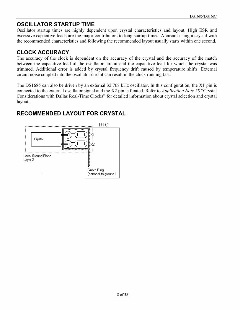
OSCILLATOR STARTUP TIMEOscillator startup times are highly dependent upon crystal characteristics and layout. High ESR andexcessive capacitive loads are the major contributors to long startup times. A circuit using a crystal withthe recommended characteristics and following the recommended layout usually starts within one second.
CLOCK ACCURACYThe accuracy of the clock is dependent on the accuracy of the crystal and the accuracy of the matchbetween the capacitive load of the oscillator circuit and the capacitive load for which the crystal wastrimmed. Additional error is added by crystal frequency drift caused by temperature shifts. Externalcircuit noise coupled into the oscillator circuit can result in the clock running fast.
The DS1685 can also be driven by an external 32.768 kHz oscillator. In this configuration, the X1 pin isconnected to the external oscillator signal and the X2 pin is floated. Refer to Application Note 58 “CrystalConsiderations with Dallas Real-Time Clocks” for detailed information about crystal selection and crystallayout.
RECOMMENDED LAYOUT FOR CRYSTAL
DS1685/DS1687
9 of 38
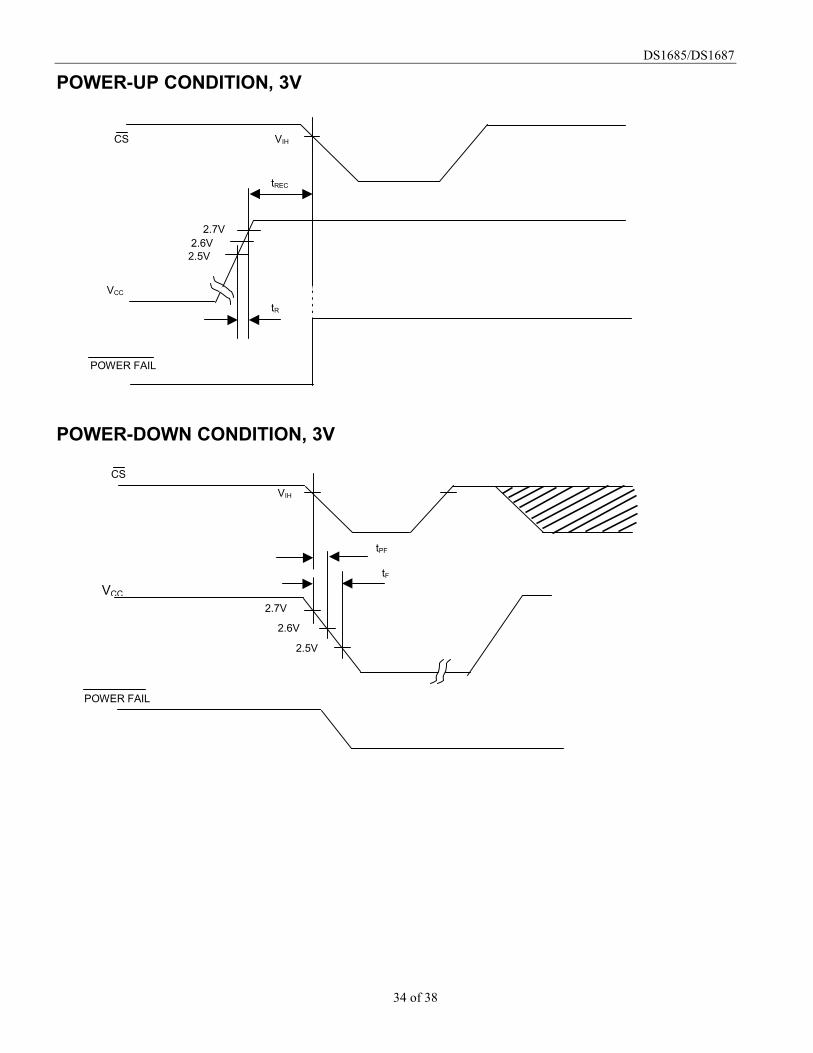
POWER-DOWN/POWER-UP CONSIDERATIONSThe RTC function continues to operate, and all of the RAM, time, calendar, and alarm memory locationsremain nonvolatile regardless of the level of the VCC input. When VCC is applied to the DS1685/DS1687and reaches a level of greater than VPF (power-fail trip point), the device becomes accessible after tREC,provided that the oscillator is running and the oscillator countdown chain is not in reset (Register A). Thistime period allows the system to stabilize after power is applied.
The DS1685/DS1687 is available in either a 3V or a 5V device.
The 5V device is fully accessible and data can be written and read only when VCC is greater than 4.5V.When VCC is below 4.5V, read and writes are inhibited. However, the timekeeping function continuesunaffected by the lower input voltage. As VCC falls below the greater of VBAT and VBAUX, the RAM andtimekeeper are switched over to a lithium battery connected either to the VBAT pin or VBAUX pin.
The 3V device is fully accessible and data can be written or read only when VCC is greater than 2.7V.When VCC falls below VPF, access to the device is inhibited. If VPF is less than VBAT and VBAUX, thepower supply is switched from VCC to the backup supply (the greater of VBAT and VBAUX) when VCCdrops below VPF. If VPF is greater than VBAT and VBAUX, the power supply is switched from VCC to thebackup supply when VCC drops below the larger of VBAT and VBAUX.
When VCC falls below VPF, the chip is write-protected. With the possible exception of the KS , PWR , andSQW pins, all inputs are ignored and all outputs are in a high-impedance state.
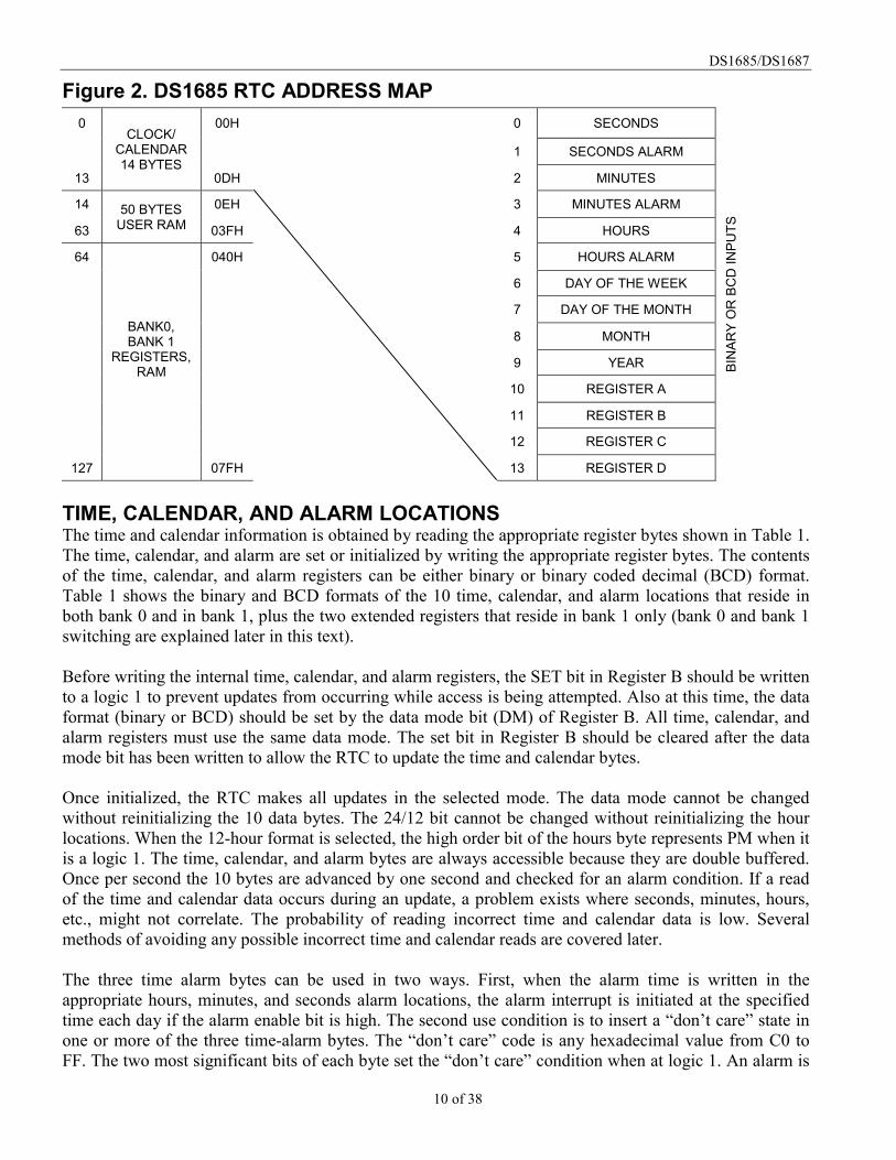
RTC ADDRESS MAPThe address map for the RTC registers of the DS1685/DS1687 is shown in Figure 2. The address mapconsists of the 14 clock/calendar registers. Ten registers contain the time, calendar, and alarm data, andfour bytes are used for control and status. All registers can be directly written or read except for thefollowing:
1) Registers C and D are read-only.2) Bit 7 of Register A is read-only.3) The high order bit of the seconds byte is read-only.
DS1685/DS1687
10 of 38
Figure 2. DS1685 RTC ADDRESS MAP0 00H 0 SECONDS
1 SECONDS ALARM
13
CLOCK/CALENDAR14 BYTES
0DH 2 MINUTES
14 0EH 3 MINUTES ALARM
6350 BYTES
USER RAM 03FH 4 HOURS
64 040H 5 HOURS ALARM
6 DAY OF THE WEEK
7 DAY OF THE MONTH
8 MONTH
9 YEAR
BANK0,BANK 1
REGISTERS,RAM
10 REGISTER A
11 REGISTER B
12 REGISTER C
127 07FH 13 REGISTER D
BIN
ARY
OR
BC
D IN
PUTS
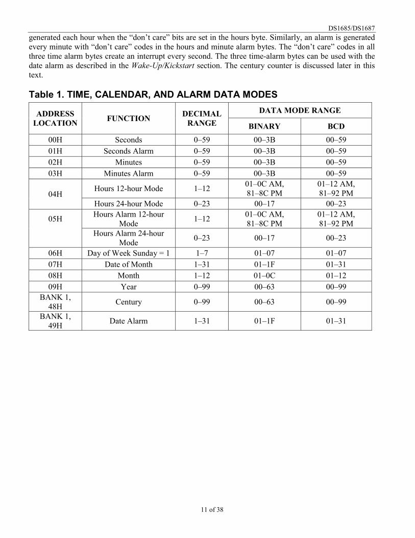
TIME, CALENDAR, AND ALARM LOCATIONSThe time and calendar information is obtained by reading the appropriate register bytes shown in Table 1.The time, calendar, and alarm are set or initialized by writing the appropriate register bytes. The contentsof the time, calendar, and alarm registers can be either binary or binary coded decimal (BCD) format.Table 1 shows the binary and BCD formats of the 10 time, calendar, and alarm locations that reside inboth bank 0 and in bank 1, plus the two extended registers that reside in bank 1 only (bank 0 and bank 1switching are explained later in this text).
Before writing the internal time, calendar, and alarm registers, the SET bit in Register B should be writtento a logic 1 to prevent updates from occurring while access is being attempted. Also at this time, the dataformat (binary or BCD) should be set by the data mode bit (DM) of Register B. All time, calendar, andalarm registers must use the same data mode. The set bit in Register B should be cleared after the datamode bit has been written to allow the RTC to update the time and calendar bytes.
Once initialized, the RTC makes all updates in the selected mode. The data mode cannot be changedwithout reinitializing the 10 data bytes. The 24/12 bit cannot be changed without reinitializing the hourlocations. When the 12-hour format is selected, the high order bit of the hours byte represents PM when itis a logic 1. The time, calendar, and alarm bytes are always accessible because they are double buffered.Once per second the 10 bytes are advanced by one second and checked for an alarm condition. If a readof the time and calendar data occurs during an update, a problem exists where seconds, minutes, hours,etc., might not correlate. The probability of reading incorrect time and calendar data is low. Severalmethods of avoiding any possible incorrect time and calendar reads are covered later.
The three time alarm bytes can be used in two ways. First, when the alarm time is written in theappropriate hours, minutes, and seconds alarm locations, the alarm interrupt is initiated at the specifiedtime each day if the alarm enable bit is high. The second use condition is to insert a “don’t care” state inone or more of the three time-alarm bytes. The “don’t care” code is any hexadecimal value from C0 toFF. The two most significant bits of each byte set the “don’t care” condition when at logic 1. An alarm is
DS1685/DS1687
11 of 38
generated each hour when the “don’t care” bits are set in the hours byte. Similarly, an alarm is generatedevery minute with “don’t care” codes in the hours and minute alarm bytes. The “don’t care” codes in allthree time alarm bytes create an interrupt every second. The three time-alarm bytes can be used with thedate alarm as described in the Wake-Up/Kickstart section. The century counter is discussed later in thistext.
Table 1. TIME, CALENDAR, AND ALARM DATA MODESDATA MODE RANGEADDRESS
LOCATION FUNCTION DECIMALRANGE BINARY BCD
00H Seconds 0–59 00–3B 00–5901H Seconds Alarm 0–59 00–3B 00–5902H Minutes 0–59 00–3B 00–5903H Minutes Alarm 0–59 00–3B 00–59
Hours 12-hour Mode 1–12 01–0C AM,81–8C PM
01–12 AM,81–92 PM04H
Hours 24-hour Mode 0–23 00–17 00–23
05H Hours Alarm 12-hourMode 1–12 01–0C AM,
81–8C PM01–12 AM,81–92 PM
Hours Alarm 24-hourMode 0–23 00–17 00–23
06H Day of Week Sunday = 1 1–7 01–07 01–0707H Date of Month 1–31 01–1F 01–3108H Month 1–12 01–0C 01–1209H Year 0–99 00–63 00–99
BANK 1,48H Century 0–99 00–63 00–99
BANK 1,49H Date Alarm 1–31 01–1F 01–31
DS1685/DS1687
12 of 38
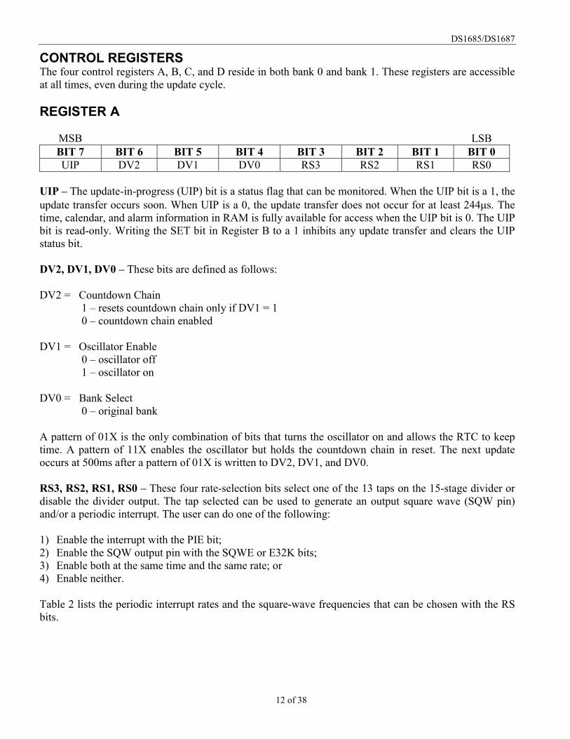
CONTROL REGISTERSThe four control registers A, B, C, and D reside in both bank 0 and bank 1. These registers are accessibleat all times, even during the update cycle.
REGISTER A
MSB LSBBIT 7 BIT 6 BIT 5 BIT 4 BIT 3 BIT 2 BIT 1 BIT 0UIP DV2 DV1 DV0 RS3 RS2 RS1 RS0
UIP – The update-in-progress (UIP) bit is a status flag that can be monitored. When the UIP bit is a 1, theupdate transfer occurs soon. When UIP is a 0, the update transfer does not occur for at least 244�s. Thetime, calendar, and alarm information in RAM is fully available for access when the UIP bit is 0. The UIPbit is read-only. Writing the SET bit in Register B to a 1 inhibits any update transfer and clears the UIPstatus bit.
DV2, DV1, DV0 – These bits are defined as follows:
DV2 = Countdown Chain1 – resets countdown chain only if DV1 = 10 – countdown chain enabled
DV1 = Oscillator Enable0 – oscillator off1 – oscillator on
DV0 = Bank Select0 – original bank
A pattern of 01X is the only combination of bits that turns the oscillator on and allows the RTC to keeptime. A pattern of 11X enables the oscillator but holds the countdown chain in reset. The next updateoccurs at 500ms after a pattern of 01X is written to DV2, DV1, and DV0.
RS3, RS2, RS1, RS0 – These four rate-selection bits select one of the 13 taps on the 15-stage divider ordisable the divider output. The tap selected can be used to generate an output square wave (SQW pin)and/or a periodic interrupt. The user can do one of the following:
1) Enable the interrupt with the PIE bit;2) Enable the SQW output pin with the SQWE or E32K bits;3) Enable both at the same time and the same rate; or4) Enable neither.
Table 2 lists the periodic interrupt rates and the square-wave frequencies that can be chosen with the RSbits.
DS1685/DS1687
13 of 38
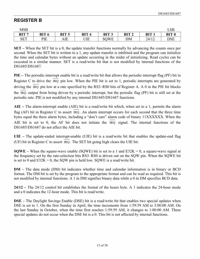
REGISTER B
MSB LSBBIT 7 BIT 6 BIT 5 BIT 4 BIT 3 BIT 2 BIT 1 BIT 0SET PIE AIE UIE SQWE DM 24/12 DSE
SET – When the SET bit is a 0, the update transfer functions normally by advancing the counts once persecond. When the SET bit is written to a 1, any update transfer is inhibited and the program can initializethe time and calendar bytes without an update occurring in the midst of initializing. Read cycles can beexecuted in a similar manner. SET is a read/write bit that is not modified by internal functions of theDS1685/DS1687.
PIE – The periodic-interrupt enable bit is a read/write bit that allows the periodic-interrupt flag (PF) bit inRegister C to drive the IRQ pin low. When the PIE bit is set to 1, periodic interrupts are generated bydriving the IRQ pin low at a rate specified by the RS3–RS0 bits of Register A. A 0 in the PIE bit blocksthe IRQ output from being driven by a periodic interrupt, but the periodic flag (PF) bit is still set at theperiodic rate. PIE is not modified by any internal DS1685/DS1687 functions.
AIE – The alarm-interrupt enable (AIE) bit is a read/write bit which, when set to a 1, permits the alarmflag (AF) bit in Register C to assert IRQ . An alarm interrupt occurs for each second that the three timebytes equal the three alarm bytes, including a “don’t care” alarm code of binary 11XXXXXX. When theAIE bit is set to 0, the AF bit does not initiate the IRQ signal. The internal functions of theDS1685/DS1687 do not affect the AIE bit.
UIE – The update-ended interrupt-enable (UIE) bit is a read/write bit that enables the update-end flag(UF) bit in Register C to assert IRQ . The SET bit going high clears the UIE bit.
SQWE – When the square-wave enable (SQWE) bit is set to a 1 and E32K = 0, a square-wave signal atthe frequency set by the rate-selection bits RS3–RS0 is driven out on the SQW pin. When the SQWE bitis set to 0 and E32K = 0, the SQW pin is held low. SQWE is a read/write bit.
DM – The data mode (DM) bit indicates whether time and calendar information is in binary or BCDformat. The DM bit is set by the program to the appropriate format and can be read as required. This bit isnot modified by internal functions. A 1 in DM signifies binary data while a 0 in DM specifies BCD data.
24/12 – The 24/12 control bit establishes the format of the hours byte. A 1 indicates the 24-hour modeand a 0 indicates the 12-hour mode. This bit is read/write.
DSE – The Daylight Savings Enable (DSE) bit is a read/write bit that enables two special updates whenDSE is set to 1. On the first Sunday in April, the time increments from 1:59:59 AM to 3:00:00 AM. Onthe last Sunday in October, when the time first reaches 1:59:59 AM, it changes to 1:00:00 AM. Thesespecial updates do not occur when the DSE bit is a 0. This bit is not affected by internal functions.
DS1685/DS1687
14 of 38
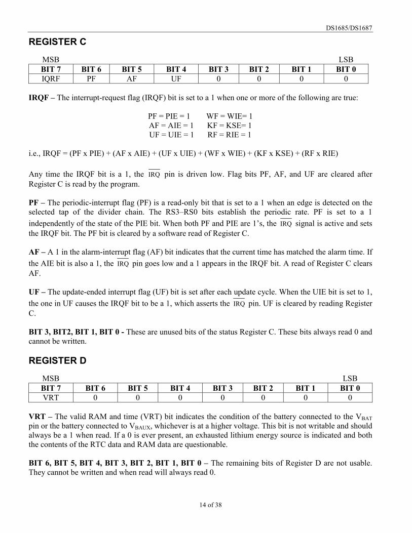
REGISTER C
MSB LSBBIT 7 BIT 6 BIT 5 BIT 4 BIT 3 BIT 2 BIT 1 BIT 0IQRF PF AF UF 0 0 0 0
IRQF – The interrupt-request flag (IRQF) bit is set to a 1 when one or more of the following are true:
PF = PIE = 1 WF = WIE= 1AF = AIE = 1 KF = KSE= 1UF = UIE = 1 RF = RIE = 1
i.e., IRQF = (PF x PIE) + (AF x AIE) + (UF x UIE) + (WF x WIE) + (KF x KSE) + (RF x RIE)
Any time the IRQF bit is a 1, the IRQ pin is driven low. Flag bits PF, AF, and UF are cleared afterRegister C is read by the program.
PF – The periodic-interrupt flag (PF) is a read-only bit that is set to a 1 when an edge is detected on theselected tap of the divider chain. The RS3–RS0 bits establish the periodic rate. PF is set to a 1independently of the state of the PIE bit. When both PF and PIE are 1’s, the IRQ signal is active and setsthe IRQF bit. The PF bit is cleared by a software read of Register C.
AF – A 1 in the alarm-interrupt flag (AF) bit indicates that the current time has matched the alarm time. Ifthe AIE bit is also a 1, the IRQ pin goes low and a 1 appears in the IRQF bit. A read of Register C clearsAF.
UF – The update-ended interrupt flag (UF) bit is set after each update cycle. When the UIE bit is set to 1,the one in UF causes the IRQF bit to be a 1, which asserts the IRQ pin. UF is cleared by reading RegisterC.
BIT 3, BIT2, BIT 1, BIT 0 - These are unused bits of the status Register C. These bits always read 0 andcannot be written.
REGISTER D
MSB LSBBIT 7 BIT 6 BIT 5 BIT 4 BIT 3 BIT 2 BIT 1 BIT 0VRT 0 0 0 0 0 0 0
VRT – The valid RAM and time (VRT) bit indicates the condition of the battery connected to the VBATpin or the battery connected to VBAUX, whichever is at a higher voltage. This bit is not writable and shouldalways be a 1 when read. If a 0 is ever present, an exhausted lithium energy source is indicated and boththe contents of the RTC data and RAM data are questionable.
BIT 6, BIT 5, BIT 4, BIT 3, BIT 2, BIT 1, BIT 0 – The remaining bits of Register D are not usable.They cannot be written and when read will always read 0.
DS1685/DS1687
15 of 38
NV RAM—RTCThe 242 general-purpose NV RAM bytes are not dedicated to any special function within theDS1685/DS1687. They can be used by the application program as nonvolatile memory and are fullyavailable during the update cycle.
The user RAM is divided into two separate memory banks. When the bank 0 is selected, the 14 RTCregisters and 114 bytes of user RAM are accessible. When bank 1 is selected, an additional 128 bytes ofuser RAM are accessible through the extended RAM address and data registers.
INTERRUPT CONTROLThe DS1685/DS1687 includes six separate, fully automatic sources of interrupt for a processor:1) Alarm Interrupt2) Periodic Interrupt3) Update-Ended Interrupt4) Wake-Up Interrupt5) Kickstart Interrupt6) RAM Clear Interrupt
The conditions that generate each of these independent interrupt conditions are described in greater detailelsewhere in this data sheet. This section describes the overall control of the interrupts.
The application software can select which interrupts, if any, are to be used. There are a total of 6 bits,including 3 bits in Register B and 3 bits in Extended Register B, that enable the interrupts. The extendedregister locations are described later. Writing a logic 1 to an interrupt-enable bit permits that interrupt tobe initiated when the event occurs. A logic 0 in the interrupt enable bit prohibits the IRQ pin from beingasserted from that interrupt condition. If an interrupt flag is already set when an interrupt is enabled, IRQ
is immediately set at an active level, even though the event initiating the interrupt condition might haveoccurred much earlier. As a result, there are cases where the software should clear these earlier generatedinterrupts before first enabling new interrupts.
When an interrupt event occurs, the relating flag bit is set to a logic 1 in Register C or in ExtendedRegister A. These flag bits are set regardless of the setting of the corresponding enable bit located eitherin Register B or in Extended Register B. The flag bits can be used in a polling mode without enabling thecorresponding enable bits.
However, care should be taken when using the flag bits of Register C as they are automatically cleared to0 immediately after they are read. Double latching is implemented on these bits so that set bits remainstable throughout the read cycle. All bits that were set are cleared when read and new interrupts that arepending during the read cycle are held until after the cycle is completed. One, two, or three bits can be setwhen reading Register C. Each used flag bit should be examined when read to ensure that no interruptsare lost.
The flag bits in Extended Register A are not automatically cleared following a read. Instead, each flag bitcan be cleared to 0 only by writing 0 to that bit.
DS1685/DS1687
16 of 38
When using the flag bits with fully enabled interrupts, the IRQ line is driven low when an interrupt flagbit is set and its corresponding enable bit is also set. IRQ is held low as long as at least one of the sixpossible interrupt sources has its flag and enable bits both set. The IRQF bit in Register C is a 1 wheneverthe IRQ pin is being driven low as a result of one of the six possible active sources. Therefore,determination that the DS1685/DS1687 initiated an interrupt is accomplished by reading Register C andfinding IRQF = 1. IRQF remains set until all enabled interrupt flag bits are cleared to 0.
SQUARE-WAVE OUTPUT SELECTIONThe SQW pin can be programmed to output a variety of frequencies divided down from the 32.768kHzcrystal tied to X1 and X2. The square-wave output is enabled and disabled by the SQWE bit in Register Bor the E32K bit in extended register 4Bh. If the square wave is enabled (SQWE = 1 or E32K = 1), thenthe output frequency is determined by the settings of the E32K bit in Extended Register 4Bh and by theRS3–0 bits in Register A. If E32K = 1, then a 32.768kHz square wave is output on the SQW pinregardless of the settings of RS3–0 and SQWE.
If E32K = 0, then the square-wave output frequency is determined by the RS3–0 bits. These bits control a1-of-15 decoder, which selects one of 13 taps that divide the 32.768kHz frequency. The RS3–0 bitsestablish the SQW output frequency as shown in Table 2. In addition, RS3–0 bits control the periodicinterrupt selection as described below.
If E32K = 1 and the auxiliary-battery enable bit (ABE, bank 1; register 04BH) is enabled, and voltage isapplied to VBAUX, then the 32kHz square-wave output signal is output on the SQW pin in the absence ofVCC. This facility is provided to clock external power management circuitry. If any of the aboverequirements are not met, no square-wave output signal is generated on the SQW pin in the absence ofVCC.
A pattern of 01X in the DV2, DV1, and DV0 bits respectively turns the oscillator on and enables thecountdown chain. Note that this is different than the DS1287, which required a pattern of 010 in thesebits. DV0 is now a “don’t care” because it is used for selection between register banks 0 and 1.
A pattern of 11X turns the oscillator on, but the oscillator’s countdown chain is held in reset, as it was inthe DS1287. Any other bit combination for DV2 and DV1 keeps the oscillator off.
Oscillator Control BitsWhen the DS1687 is shipped from the factory, the internal oscillator is turned off. This feature preventsthe lithium energy cell from being used until it is installed in a system. A pattern of 01X in bits 4 through6 of Register A turns the oscillator on and enables the countdown chain. A pattern of 11X turns theoscillator on, but holds the countdown chain of the oscillator in reset. All other combinations of bits 4through 6 keep the oscillator off.
PERIODIC INTERRUPT SELECTIONThe periodic interrupt causes the IRQ pin to go to an active state from once every 500ms to once every122�s. This function is separate from the alarm interrupt, which can be output from once per second toonce per day. The periodic interrupt rate is selected using the same RS3–0 bits in Register A, which selectthe square-wave frequency (Table 2). Changing the bits affects both the square-wave frequency and theperiodic-interrupt output. However, each function has a separate enable bit in Register B. The SQWE andE32K bits control the square-wave output. Similarly, the periodic interrupt is enabled by the PIE bit in
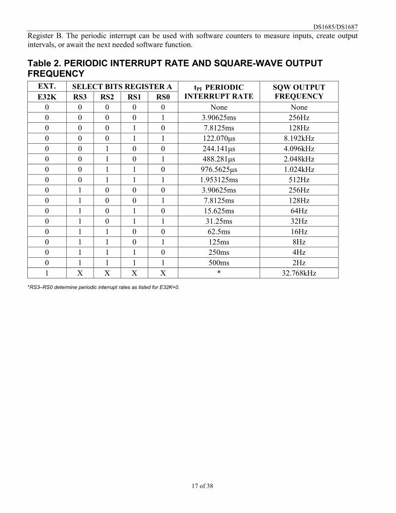
DS1685/DS1687
17 of 38
Register B. The periodic interrupt can be used with software counters to measure inputs, create outputintervals, or await the next needed software function.
Table 2. PERIODIC INTERRUPT RATE AND SQUARE-WAVE OUTPUTFREQUENCY
EXT. SELECT BITS REGISTER AE32K RS3 RS2 RS1 RS0
tPI PERIODICINTERRUPT RATE
SQW OUTPUTFREQUENCY
0 0 0 0 0 None None0 0 0 0 1 3.90625ms 256Hz0 0 0 1 0 7.8125ms 128Hz0 0 0 1 1 122.070µs 8.192kHz0 0 1 0 0 244.141µs 4.096kHz0 0 1 0 1 488.281µs 2.048kHz0 0 1 1 0 976.5625µs 1.024kHz0 0 1 1 1 1.953125ms 512Hz0 1 0 0 0 3.90625ms 256Hz0 1 0 0 1 7.8125ms 128Hz0 1 0 1 0 15.625ms 64Hz0 1 0 1 1 31.25ms 32Hz0 1 1 0 0 62.5ms 16Hz0 1 1 0 1 125ms 8Hz0 1 1 1 0 250ms 4Hz0 1 1 1 1 500ms 2Hz1 X X X X * 32.768kHz
*RS3–RS0 determine periodic interrupt rates as listed for E32K=0.
DS1685/DS1687
18 of 38
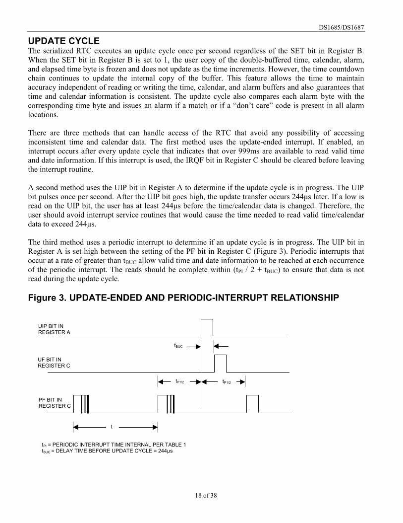
UPDATE CYCLEThe serialized RTC executes an update cycle once per second regardless of the SET bit in Register B.When the SET bit in Register B is set to 1, the user copy of the double-buffered time, calendar, alarm,and elapsed time byte is frozen and does not update as the time increments. However, the time countdownchain continues to update the internal copy of the buffer. This feature allows the time to maintainaccuracy independent of reading or writing the time, calendar, and alarm buffers and also guarantees thattime and calendar information is consistent. The update cycle also compares each alarm byte with thecorresponding time byte and issues an alarm if a match or if a “don’t care” code is present in all alarmlocations.
There are three methods that can handle access of the RTC that avoid any possibility of accessinginconsistent time and calendar data. The first method uses the update-ended interrupt. If enabled, aninterrupt occurs after every update cycle that indicates that over 999ms are available to read valid timeand date information. If this interrupt is used, the IRQF bit in Register C should be cleared before leavingthe interrupt routine.
A second method uses the UIP bit in Register A to determine if the update cycle is in progress. The UIPbit pulses once per second. After the UIP bit goes high, the update transfer occurs 244µs later. If a low isread on the UIP bit, the user has at least 244µs before the time/calendar data is changed. Therefore, theuser should avoid interrupt service routines that would cause the time needed to read valid time/calendardata to exceed 244µs.
The third method uses a periodic interrupt to determine if an update cycle is in progress. The UIP bit inRegister A is set high between the setting of the PF bit in Register C (Figure 3). Periodic interrupts thatoccur at a rate of greater than tBUC allow valid time and date information to be reached at each occurrenceof the periodic interrupt. The reads should be complete within (tPI / 2 + tBUC) to ensure that data is notread during the update cycle.
Figure 3. UPDATE-ENDED AND PERIODIC-INTERRUPT RELATIONSHIP
t
tP1/2 tP1/2
tBUC
UIP BIT INREGISTER A
UF BIT INREGISTER C
PF BIT INREGISTER C
tPI = PERIODIC INTERRUPT TIME INTERNAL PER TABLE 1tBUC = DELAY TIME BEFORE UPDATE CYCLE = 244µs
DS1685/DS1687
19 of 38
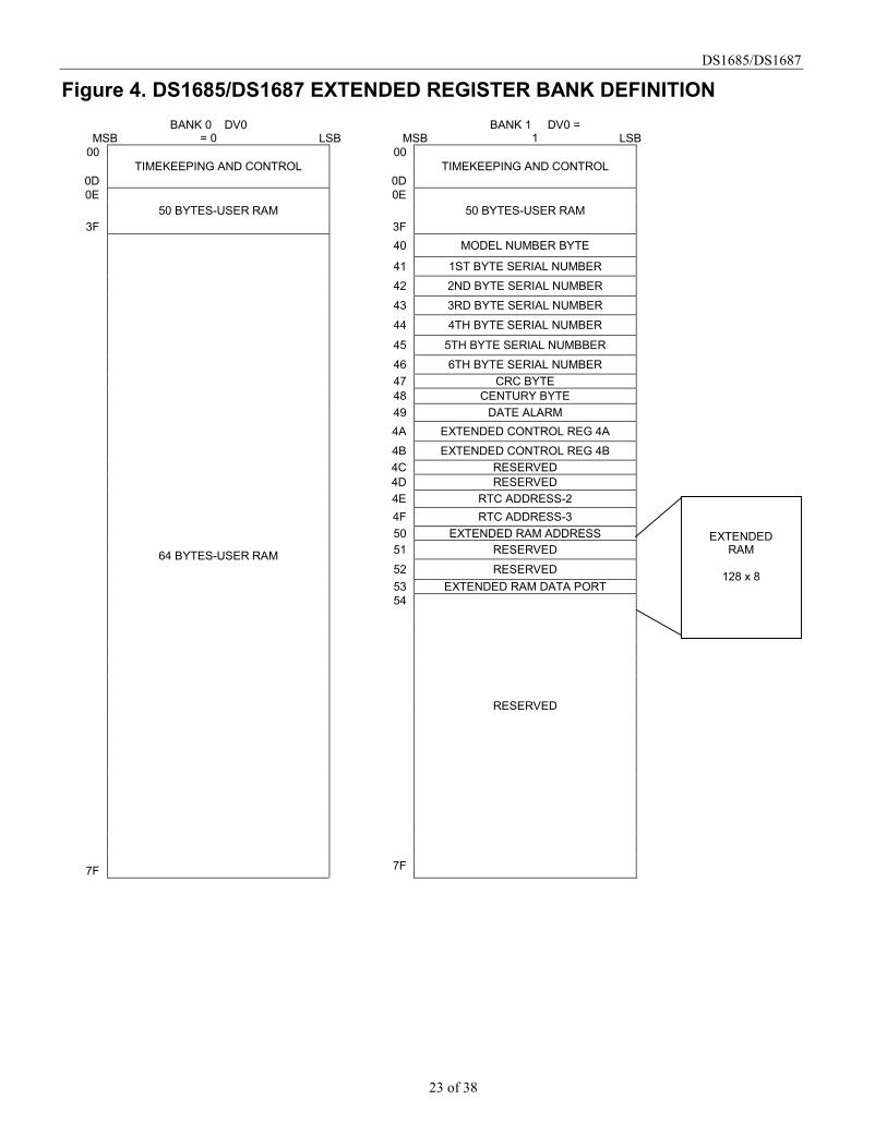
EXTENDED FUNCTIONSThe extended functions provided by the DS1685/DS1687 that are new to the RAMified RTC family areaccessed by a software-controlled bank-switching scheme, as illustrated in Figure 4. In bank 0, theclock/calendar registers and 50 bytes of user RAM are in the same locations as for the DS1287. As aresult, existing routines implemented within BIOS, DOS, or application software packages can gainaccess to the DS1685/DS1687 clock registers with no changes. Also in bank 0, an extra 64 bytes of RAMare provided at addresses just above the original locations for a total of 114 directly addressable bytes ofuser RAM.
When bank 1 is selected, the clock/calendar registers and the original 50 bytes of user RAM still appearas bank 0. However, the Dallas registers that provide control and status for the extended functions areaccessed in place of the additional 64 bytes of user RAM. The major extended functions controlled by theDallas registers are listed below:
1) 64-bit Silicon Serial Number2) Century counter3) Date Alarm4) Auxiliary Battery Control/Status5) Wake-Up6) Kickstart7) RAM Clear Control/Status8) 128-bytes Extended RAM Access
The bank selection is controlled by the state of the DV0 bit in register A. To access bank 0, the DV0 bitshould be written to a 0. To access bank 1, DV0 should be written to a 1. Register locations designated asreserved in the bank 1 map are reserved for future use by Dallas Semiconductor. Bits in these locationscannot be written and return a 0 if read.
SILICON SERIAL NUMBERA unique 64-bit lasered serial number is located in bank 1, registers 40h to 47h. This serial number isdivided into three parts. The first byte in register 40h contains a model number, 47h, to identify the devicetype. Registers 41h to 46h contain a unique binary number. Register 47h contains a CRC byte used tovalidate the data in registers 40h to 46h. All 8 bytes of the serial number are read-only registers.
The DS1685/DS1687 is manufactured such that no two devices contain an identical number in locations41h to 47h.
CENTURY COUNTERA register has been added in bank 1, location 48H, to keep track of centuries. The value is read in eitherbinary or BCD according to the setting of the DM bit.
DS1685/DS1687
20 of 38
AUXILIARY BATTERYThe VBAUX input is provided to supply power from an auxiliary battery for the DS1685/DS1687 kickstart,wake-up, and SQW output features in the absence of VCC. This power source must be available in orderto use these auxiliary features when no VCC is applied to the device.
The auxiliary-battery enable (ABE; bank 1, register 04BH) bit in extended control register B is used toturn on and off the auxiliary battery for the above functions in the absence of VCC. When set to a 1, VBAUXbattery power is enabled, and when cleared to 0, VBAUX battery power is disabled to these functions.
In the DS1685/DS1687, this auxiliary battery can be used as the primary backup-power source formaintaining the clock/calendar, user RAM, and extended external RAM functions. This occurs if theVBAT pin is at a lower voltage than VBAUX. If the DS1685 is to be backed-up using a single battery withthe auxiliary features enabled, then VBAUX should be used and VBAT should be grounded. If VBAUX is notto be used, it should be grounded and ABE should be cleared to 0.
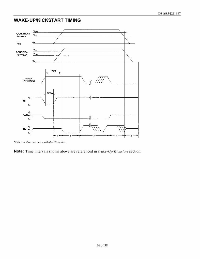
WAKE-UP/KICKSTARTThe DS1685/DS1687 incorporates a wake-up feature that can power the system on at a predetermineddate and time through activation of the PWR output pin. In addition, the kickstart feature allows thesystem to be powered up in response to a low-going transition on the KS pin, without operating voltageapplied to the VCC pin. As a result, system power can be applied upon such events as a key closure ormodem-ring detect signal. In order to use either the wake-up or the kickstart features, theDS1685/DS1687 must have an auxiliary battery connected to the VBAUX pin and the oscillator must berunning, and the countdown chain must not be in reset (Register A DV2, DV1, DV0 = 01X). If DV2,DV1, and DV0 are not in this required state, the PWR pin does not drive low in response to a kickstart orwake-up condition, while in battery-backed mode.
The wake-up feature is controlled through the wake-up interrupt-enable bit in extended control register B(WIE, bank 1, 04BH). Setting WIE to 1 enables the wake-up feature, clearing WIE to 0 disables it.Similarly, the kick-start feature is controlled through the kickstart-interrupt-enable bit in extended controlregister B (KSE, bank 1, 04BH).
A wake-up sequence occurs as follows: When wake-up is enabled by WIE = 1 while the system ispowered down (no VCC voltage), the clock/calendar monitors the current date for a match condition withthe date alarm register (bank 1, register 049H). In conjunction with the date alarm register, the hours,minutes, and seconds alarm bytes in the clock/calendar register map (bank 0, registers 05H, 03H, and01H) are also monitored. As a result, a wake-up occurs at the date and time specified by the date, hours,minutes, and seconds alarm-register values. This additional alarm occurs regardless of the programmingof the AIE bit (bank 0, register B, 0BH). When the match condition occurs, the PWR pin automaticallydrives low. This output can be used to turn on the main system power supply, which provides VCC voltageto the DS1685/DS1687 as well as the other major components in the system. Also at this time, the wake-up flag (WF, bank 1, register 04AH) is set, indicating that a wake-up condition has occurred.
A kickstart sequence occurs when kickstarting is enabled by KSE = 1. While the system is powereddown, the KS input pin is monitored for a low-going transition of minimum pulse width tKSPW. Whensuch a transition is detected, the PWR line pulls low, as it does for a wake-up condition. Also at this time,the kickstart flag (KF, bank 1, register 04AH) is set, indicating that a kickstart condition has occurred.
The timing associated with both the wake-up and kickstarting sequences is illustrated in the “Wake-
DS1685/DS1687
21 of 38
Up/Kickstart Timing Diagram” in the Electrical Specifications section of this data sheet. The timingassociated with these functions is divided into five intervals, labeled 1 to 5 on the diagram.
The occurrence of either a kickstart or wake-up condition causes the PWR pin to be driven low, asdescribed above. During Interval 1, if the supply voltage on the DS1685/DS1687 VCC pin rises above thegreater of VBAT or VPF before the power on timeout period (tPOTO) expires, then PWR remains at theactive-low level. If VCC does not rise above the greater of VBAT or VPF in this time, then the PWR outputpin is turned off and returns to its high-impedance level. In this event, the IRQ pin also remains tri-stated.The interrupt flag bit (either WF or KF) associated with the attempted power-on sequence remains setuntil cleared by software during a subsequent system power-on.
If VCC is applied within the timeout period, then the system power-on sequence continues as shown inIntervals 2 to 5 in the timing diagram. During Interval 2, PWR remains active and IRQ is driven to itsactive-low level, indicating that either WF or KF was set in initiating the power-on. In the diagram, KS isassumed to be pulled up to the VBAUX supply. Also at this time, the PAB bit is automatically cleared to 0in response to a successful power-on. The PWR line remains active as long as the PAB remains cleared to0.
At the beginning of Interval 3, the system processor has begun code execution and clears the interruptcondition of WF and/or KF by writing 0’s to both of these control bits. As long as no other interruptwithin the DS1685/DS1687 is pending, the IRQ line is taken inactive once these bits are reset. Executionof the application software can proceed. During this time, both the wake-up and kickstart functions can beused to generate status and interrupts. WF is set in response to a date, hours, minutes, and seconds matchcondition. KF is set in response to a low-going transition on KS. If the associated interrupt-enable bit isset (WIE and/or KSE), then the IRQ line is driven active-low in response to enabled event. In addition,the other possible interrupt sources within the DS1685/DS1687 can cause IRQ to be driven low. Whilesystem power is applied, the on-chip logic always attempts to drive the PWR pin active in response to theenabled kickstart or wake-up condition. This is true even if PWR was previously inactive as the result ofpower being applied by some means other than wake-up or kickstart.
The system can be powered down under software control by setting the PAB bit to a logic 1. This causesthe open-drain PWR pin to be placed in a high-impedance state, as shown at the beginning of Interval 4 inthe timing diagram. As VCC voltage decays, the IRQ output pin is placed in a high-impedance state whenVCC goes below VPF. If the system is to be again powered on in response to a wake-up or kickstart, thenthe both the WF and KF flags should be cleared and WIE and/or KSE should be enabled prior to settingthe PAB bit.
During Interval 5, the system is fully powered down. Battery backup of the clock calendar and NV RAMis in effect and IRQ is tri-stated, and monitoring of wake-up and kickstart takes place. If PRS = 1, PWR
stays active; otherwise, if PRS = 0, PWR is tri-stated.
RAM CLEARThe DS1685/DS1687 provides a RAM clear function for the 242 bytes of user RAM. When enabled, thisfunction can be performed regardless of the condition of the VCC pin.
DS1685/DS1687
22 of 38
The RAM clear function is enabled or disabled by the RAM clear-enable bit (RCE; bank 1, register04BH). When this bit is set to a logic 1, the 242 bytes of user RAM is cleared (all bits set to 1) when anactive-low transition is sensed on the RCLR pin. This action has no affect on either the clock/calendarsettings or upon the contents of the extended RAM. The RAM clear flag (RF, bank 1, register 04AH) isset when the RAM clear operation has been completed. If VCC is present at the time of the RAM clear andRIE = 1, the IRQ line is also driven low upon completion. The interrupt condition can be cleared bywriting a 0 to the RF bit. The IRQ line then returns to its inactive high level, provided there are no otherpending interrupts. Once the RCLR pin is activated, all read/write accesses are locked out for a minimumrecover time, specified as tREC in the Electrical Characteristics section.
When RCE is cleared to 0, the RAM clear function is disabled. The state of the RCLR pin has no affecton the contents of the user RAM, and transitions on the RCLR pin have no affect on RF.
128 x 8 EXTENDED RAMThe DS1685/DS1687 provides 128 x 8 of on-chip SRAM, which is controlled as nonvolatile storagesustained from a lithium battery. On power-up, the RAM is taken out of write-protect status by theinternal power-OK signal (POK) generated from the write-protect circuitry.
The on-chip 128 x 8 NV SRAM is accessed by the eight multiplexed address/data lines AD7–AD0.Access to the SRAM is controlled by two on-chip latch registers. One register is used to hold the SRAMaddress and the other register is used to hold read/write data. The SRAM address space is from 00h to7Fh.
Access to the extended 128 x 8 RAM is controlled by two of the registers shown in Figure 4. Theregisters in bank 1 must first be selected by setting the DV0 bit in register A to a logic 1. The 7-bitaddress of the RAM location to be accessed must be loaded into the extended RAM address registerlocated at 50h. Data in the addressed location may be read by performing a read operation from location53h, or written to by performing a write operation to location 53h. Data in any addressed location may beread or written repeatedly without changing the address in location 50h.
DS1685/DS1687
23 of 38
Figure 4. DS1685/DS1687 EXTENDED REGISTER BANK DEFINITION
MSBBANK 0 DV0
= 0 LSB MSBBANK 1 DV0 =
1 LSB00 00
0DTIMEKEEPING AND CONTROL
0DTIMEKEEPING AND CONTROL
0E 0E
3F50 BYTES-USER RAM
3F50 BYTES-USER RAM
40 MODEL NUMBER BYTE
41 1ST BYTE SERIAL NUMBER42 2ND BYTE SERIAL NUMBER43 3RD BYTE SERIAL NUMBER44 4TH BYTE SERIAL NUMBER
45 5TH BYTE SERIAL NUMBBER46 6TH BYTE SERIAL NUMBER47 CRC BYTE48 CENTURY BYTE49 DATE ALARM4A EXTENDED CONTROL REG 4A4B EXTENDED CONTROL REG 4B4C RESERVED4D RESERVED4E RTC ADDRESS-24F RTC ADDRESS-350 EXTENDED RAM ADDRESS51 RESERVED52 RESERVED53 EXTENDED RAM DATA PORT54
RESERVED
7F
64 BYTES-USER RAM
7F
EXTENDEDRAM
128 x 8
DS1685/DS1687
24 of 38
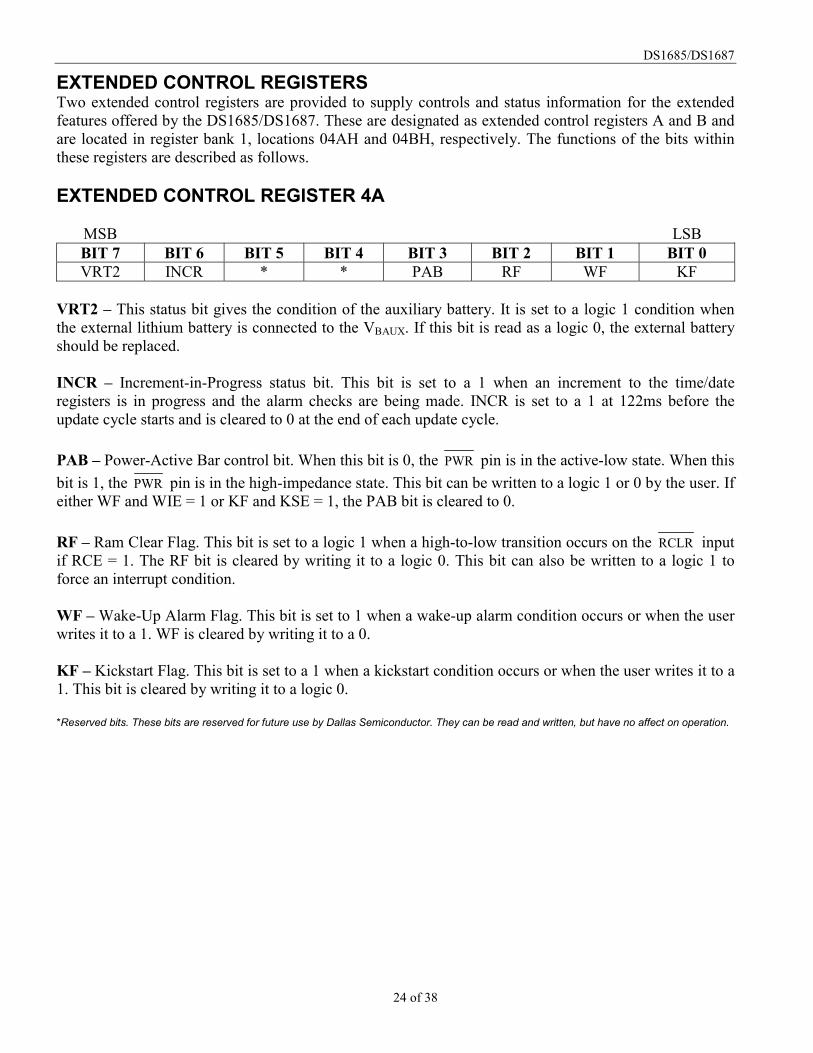
EXTENDED CONTROL REGISTERSTwo extended control registers are provided to supply controls and status information for the extendedfeatures offered by the DS1685/DS1687. These are designated as extended control registers A and B andare located in register bank 1, locations 04AH and 04BH, respectively. The functions of the bits withinthese registers are described as follows.
EXTENDED CONTROL REGISTER 4A
MSB LSBBIT 7 BIT 6 BIT 5 BIT 4 BIT 3 BIT 2 BIT 1 BIT 0VRT2 INCR * * PAB RF WF KF
VRT2 – This status bit gives the condition of the auxiliary battery. It is set to a logic 1 condition whenthe external lithium battery is connected to the VBAUX. If this bit is read as a logic 0, the external batteryshould be replaced.
INCR – Increment-in-Progress status bit. This bit is set to a 1 when an increment to the time/dateregisters is in progress and the alarm checks are being made. INCR is set to a 1 at 122ms before theupdate cycle starts and is cleared to 0 at the end of each update cycle.
PAB – Power-Active Bar control bit. When this bit is 0, the PWR pin is in the active-low state. When thisbit is 1, the PWR pin is in the high-impedance state. This bit can be written to a logic 1 or 0 by the user. Ifeither WF and WIE = 1 or KF and KSE = 1, the PAB bit is cleared to 0.
RF – Ram Clear Flag. This bit is set to a logic 1 when a high-to-low transition occurs on the RCLR inputif RCE = 1. The RF bit is cleared by writing it to a logic 0. This bit can also be written to a logic 1 toforce an interrupt condition.
WF – Wake-Up Alarm Flag. This bit is set to 1 when a wake-up alarm condition occurs or when the userwrites it to a 1. WF is cleared by writing it to a 0.
KF – Kickstart Flag. This bit is set to a 1 when a kickstart condition occurs or when the user writes it to a1. This bit is cleared by writing it to a logic 0.
*Reserved bits. These bits are reserved for future use by Dallas Semiconductor. They can be read and written, but have no affect on operation.
DS1685/DS1687
25 of 38
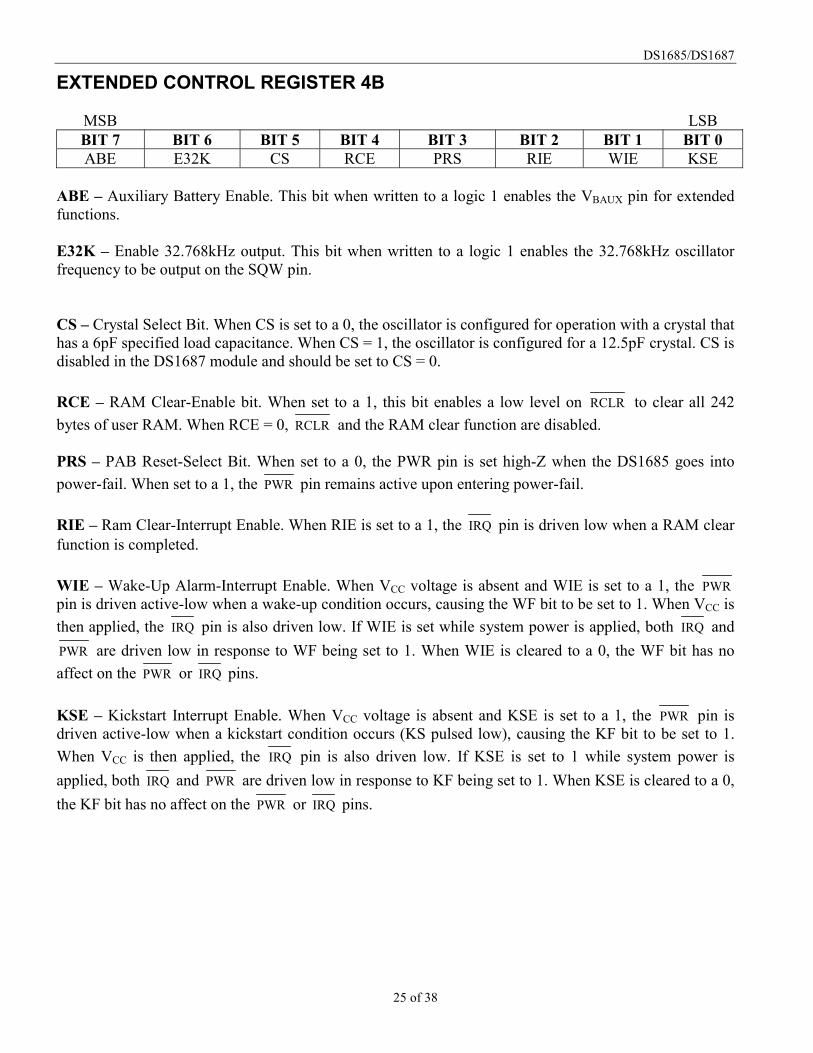
EXTENDED CONTROL REGISTER 4B
MSB LSBBIT 7 BIT 6 BIT 5 BIT 4 BIT 3 BIT 2 BIT 1 BIT 0ABE E32K CS RCE PRS RIE WIE KSE
ABE – Auxiliary Battery Enable. This bit when written to a logic 1 enables the VBAUX pin for extendedfunctions.
E32K – Enable 32.768kHz output. This bit when written to a logic 1 enables the 32.768kHz oscillatorfrequency to be output on the SQW pin.
CS – Crystal Select Bit. When CS is set to a 0, the oscillator is configured for operation with a crystal thathas a 6pF specified load capacitance. When CS = 1, the oscillator is configured for a 12.5pF crystal. CS isdisabled in the DS1687 module and should be set to CS = 0.
RCE – RAM Clear-Enable bit. When set to a 1, this bit enables a low level on RCLR to clear all 242bytes of user RAM. When RCE = 0, RCLR and the RAM clear function are disabled.
PRS – PAB Reset-Select Bit. When set to a 0, the PWR pin is set high-Z when the DS1685 goes intopower-fail. When set to a 1, the PWR pin remains active upon entering power-fail.
RIE – Ram Clear-Interrupt Enable. When RIE is set to a 1, the IRQ pin is driven low when a RAM clearfunction is completed.
WIE – Wake-Up Alarm-Interrupt Enable. When VCC voltage is absent and WIE is set to a 1, the PWRpin is driven active-low when a wake-up condition occurs, causing the WF bit to be set to 1. When VCC isthen applied, the IRQ pin is also driven low. If WIE is set while system power is applied, both IRQ andPWR are driven low in response to WF being set to 1. When WIE is cleared to a 0, the WF bit has noaffect on the PWR or IRQ pins.
KSE – Kickstart Interrupt Enable. When VCC voltage is absent and KSE is set to a 1, the PWR pin isdriven active-low when a kickstart condition occurs (KS pulsed low), causing the KF bit to be set to 1.When VCC is then applied, the IRQ pin is also driven low. If KSE is set to 1 while system power isapplied, both IRQ and PWR are driven low in response to KF being set to 1. When KSE is cleared to a 0,the KF bit has no affect on the PWR or IRQ pins.
DS1685/DS1687
26 of 38
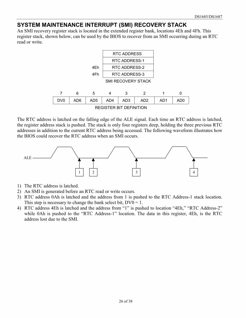
SYSTEM MAINTENANCE INTERRUPT (SMI) RECOVERY STACKAn SMI recovery register stack is located in the extended register bank, locations 4Eh and 4Fh. Thisregister stack, shown below, can be used by the BIOS to recover from an SMI occurring during an RTCread or write.
RTC ADDRESS
RTC ADDRESS-14Eh RTC ADDRESS-2
4Fh RTC ADDRESS-3
SMI RECOVERY STACK
7 6 5 4 3 2 1 0
DV0 AD6 AD5 AD4 AD3 AD2 AD1 AD0
REGISTER BIT DEFINITION
The RTC address is latched on the falling edge of the ALE signal. Each time an RTC address is latched,the register address stack is pushed. The stack is only four registers deep, holding the three previous RTCaddresses in addition to the current RTC address being accessed. The following waveform illustrates howthe BIOS could recover the RTC address when an SMI occurs.
1) The RTC address is latched.2) An SMI is generated before an RTC read or write occurs.3) RTC address 0Ah is latched and the address from 1 is pushed to the RTC Address-1 stack location.
This step is necessary to change the bank select bit, DV0 = 1.4) RTC address 4Eh is latched and the address from “1” is pushed to location “4Eh,” “RTC Address-2”
while 0Ah is pushed to the “RTC Address-1” location. The data in this register, 4Eh, is the RTCaddress lost due to the SMI.
1 2 3 4
ALE
DS1685/DS1687
27 of 38
ABSOLUTE MAXIMUM RATINGS*Voltage Range on Any Pin Relative to Ground 0.3V to +6VOperating Temperature Range, Commercial 0°C to +70°COperating Temperature Range, Industrial -40�C to +85�CStorage Temperature Range -40°C to +85°CSoldering Temperature See IPC/JEDEC J-STD-020A (Note 12)
*This is a stress rating only and functional operation of the device at these or any other conditions beyond those indicated in the operationsections of this specification is not implied. Exposure to absolute maximum rating conditions for extended periods of time can affect reliability.
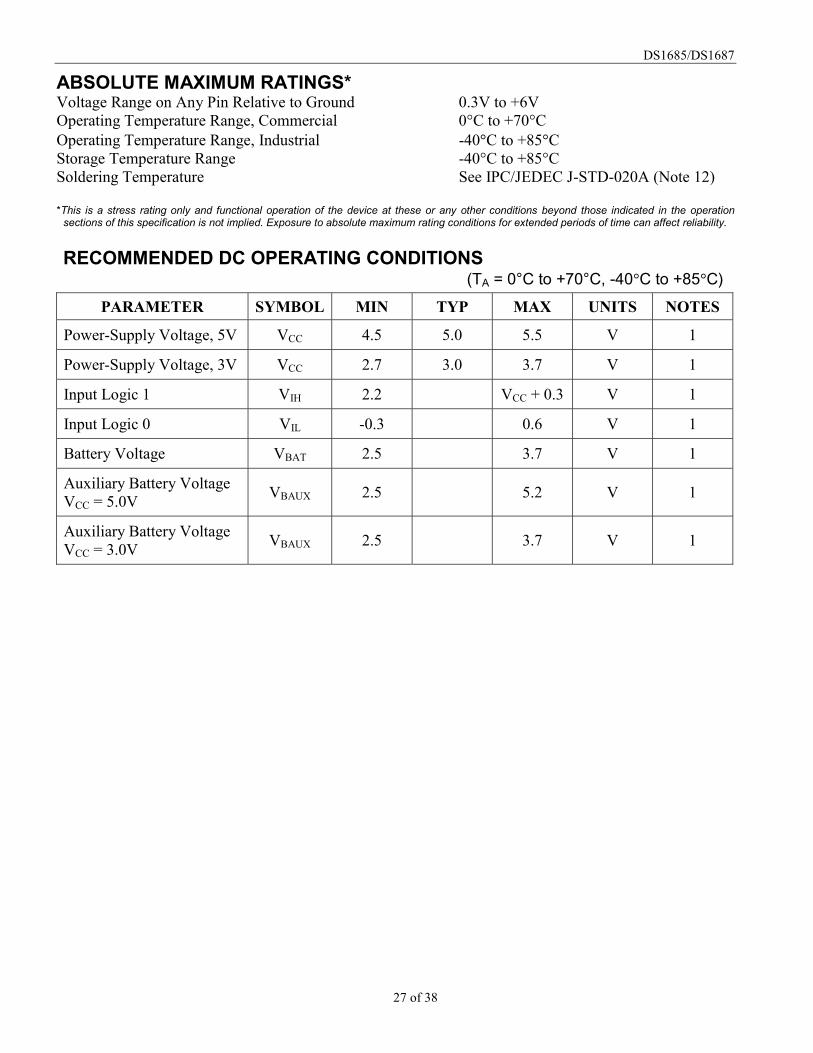
RECOMMENDED DC OPERATING CONDITIONS (TA = 0°C to +70°C, -40�C to +85�C)
PARAMETER SYMBOL MIN TYP MAX UNITS NOTES
Power-Supply Voltage, 5V VCC 4.5 5.0 5.5 V 1
Power-Supply Voltage, 3V VCC 2.7 3.0 3.7 V 1
Input Logic 1 VIH 2.2 VCC + 0.3 V 1
Input Logic 0 VIL -0.3 0.6 V 1
Battery Voltage VBAT 2.5 3.7 V 1
Auxiliary Battery VoltageVCC = 5.0V VBAUX 2.5 5.2 V 1
Auxiliary Battery VoltageVCC = 3.0V VBAUX 2.5 3.7 V 1
DS1685/DS1687
28 of 38
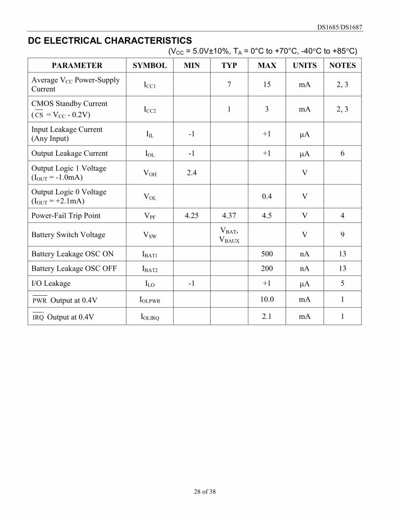
DC ELECTRICAL CHARACTERISTICS (VCC = 5.0V±10%, TA = 0°C to +70°C, -40�C to +85�C)
PARAMETER SYMBOL MIN TYP MAX UNITS NOTES
Average VCC Power-SupplyCurrent ICC1 7 15 mA 2, 3
CMOS Standby Current( CS = VCC - 0.2V)
ICC2 1 3 mA 2, 3
Input Leakage Current(Any Input) IIL -1 +1 �A
Output Leakage Current IOL -1 +1 �A 6
Output Logic 1 Voltage(IOUT = -1.0mA) VOH 2.4 V
Output Logic 0 Voltage(IOUT = +2.1mA) VOL 0.4 V
Power-Fail Trip Point VPF 4.25 4.37 4.5 V 4
Battery Switch Voltage VSWVBAT,VBAUX
V 9
Battery Leakage OSC ON IBAT1 500 nA 13
Battery Leakage OSC OFF IBAT2 200 nA 13
I/O Leakage ILO -1 +1 �A 5
PWR Output at 0.4V IOLPWR 10.0 mA 1
IRQ Output at 0.4V IOLIRQ 2.1 mA 1
DS1685/DS1687
29 of 38
DC ELECTRICAL CHARACTERISTICS (VCC = 3.0V±10%, TA = 0°C to +70°C, -40°C to +85°C)
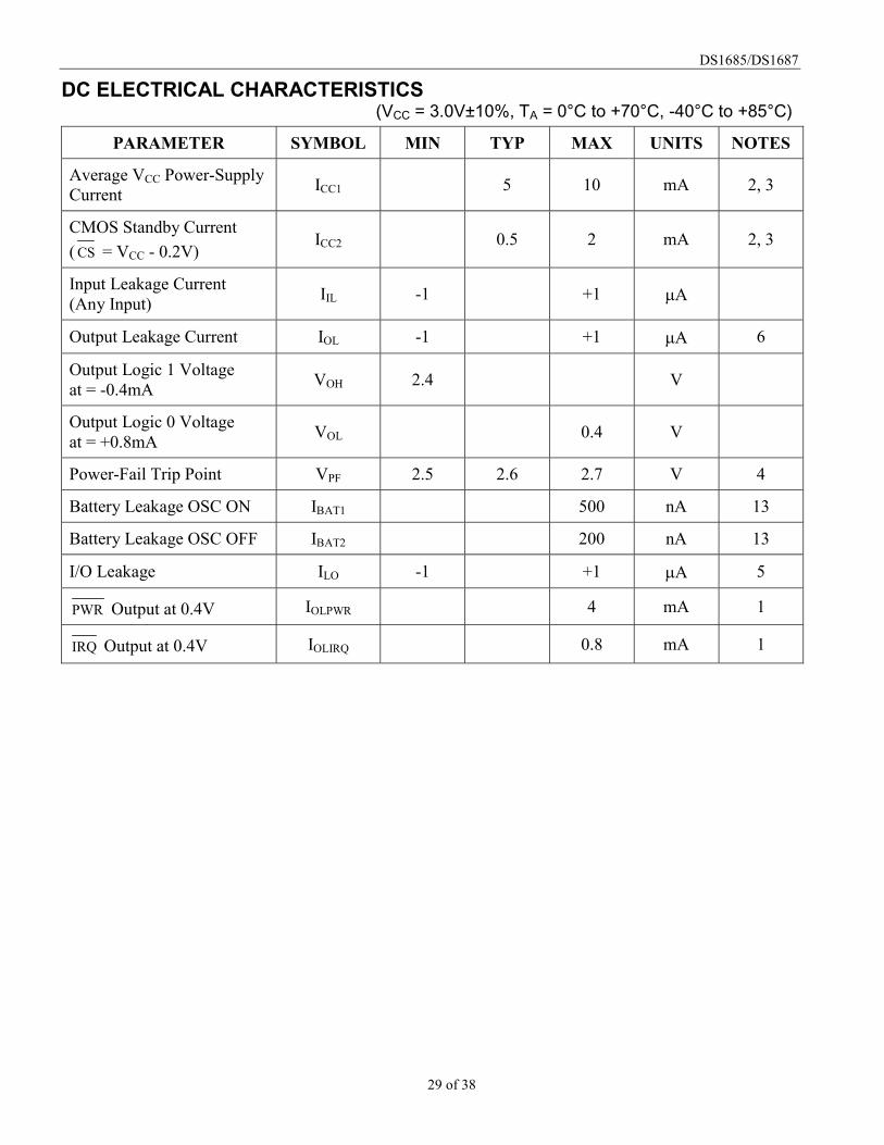
PARAMETER SYMBOL MIN TYP MAX UNITS NOTES
Average VCC Power-SupplyCurrent ICC1 5 10 mA 2, 3
CMOS Standby Current( CS = VCC - 0.2V)
ICC2 0.5 2 mA 2, 3
Input Leakage Current(Any Input) IIL -1 +1 �A
Output Leakage Current IOL -1 +1 �A 6
Output Logic 1 Voltageat = -0.4mA VOH 2.4 V
Output Logic 0 Voltageat = +0.8mA VOL 0.4 V
Power-Fail Trip Point VPF 2.5 2.6 2.7 V 4
Battery Leakage OSC ON IBAT1 500 nA 13
Battery Leakage OSC OFF IBAT2 200 nA 13
I/O Leakage ILO -1 +1 �A 5
PWR Output at 0.4V IOLPWR 4 mA 1
IRQ Output at 0.4V IOLIRQ 0.8 mA 1
DS1685/DS1687
30 of 38
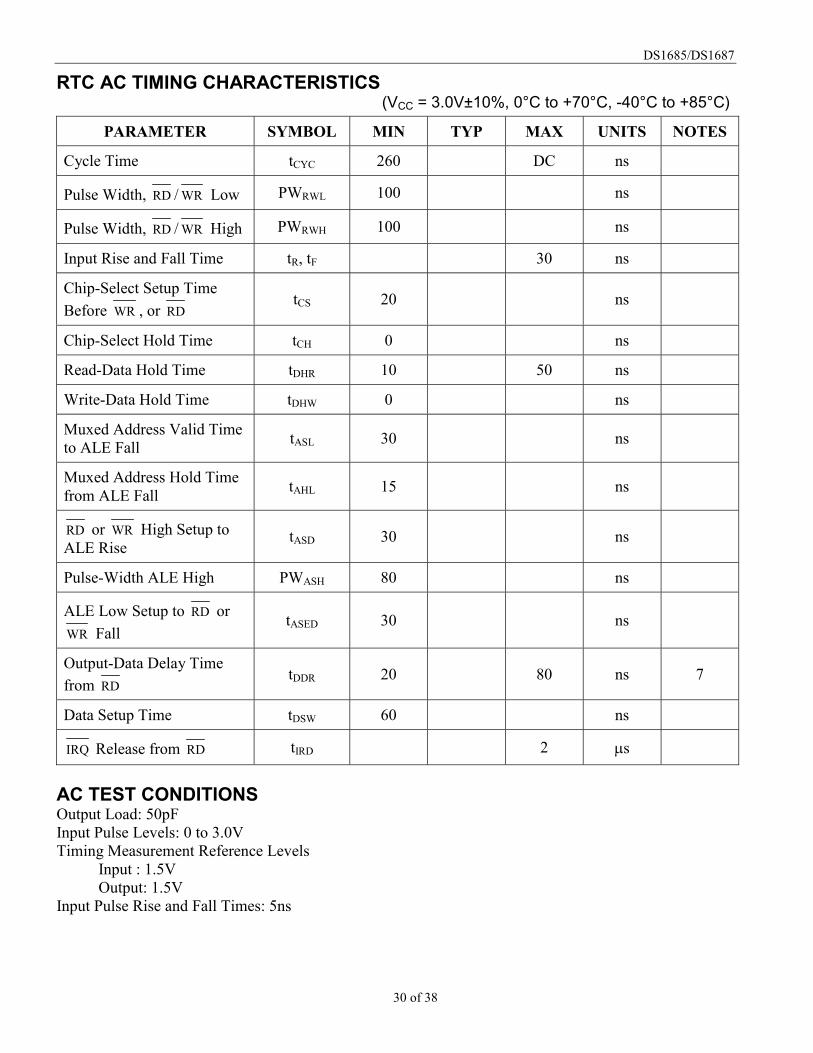
RTC AC TIMING CHARACTERISTICS (VCC = 3.0V±10%, 0°C to +70°C, -40°C to +85°C)
PARAMETER SYMBOL MIN TYP MAX UNITS NOTES
Cycle Time tCYC 260 DC ns
Pulse Width, RD / WR Low PWRWL 100 ns
Pulse Width, RD / WR High PWRWH 100 ns
Input Rise and Fall Time tR, tF 30 ns
Chip-Select Setup TimeBefore WR , or RD
tCS 20 ns
Chip-Select Hold Time tCH 0 ns
Read-Data Hold Time tDHR 10 50 ns
Write-Data Hold Time tDHW 0 ns
Muxed Address Valid Timeto ALE Fall tASL 30 ns
Muxed Address Hold Timefrom ALE Fall tAHL 15 ns
RD or WR High Setup toALE Rise
tASD 30 ns
Pulse-Width ALE High PWASH 80 ns
ALE Low Setup to RD orWR Fall
tASED 30 ns
Output-Data Delay Timefrom RD
tDDR 20 80 ns 7
Data Setup Time tDSW 60 ns
IRQ Release from RD tIRD 2 �s
AC TEST CONDITIONSOutput Load: 50pFInput Pulse Levels: 0 to 3.0VTiming Measurement Reference Levels
Input : 1.5VOutput: 1.5V
Input Pulse Rise and Fall Times: 5ns
DS1685/DS1687
31 of 38
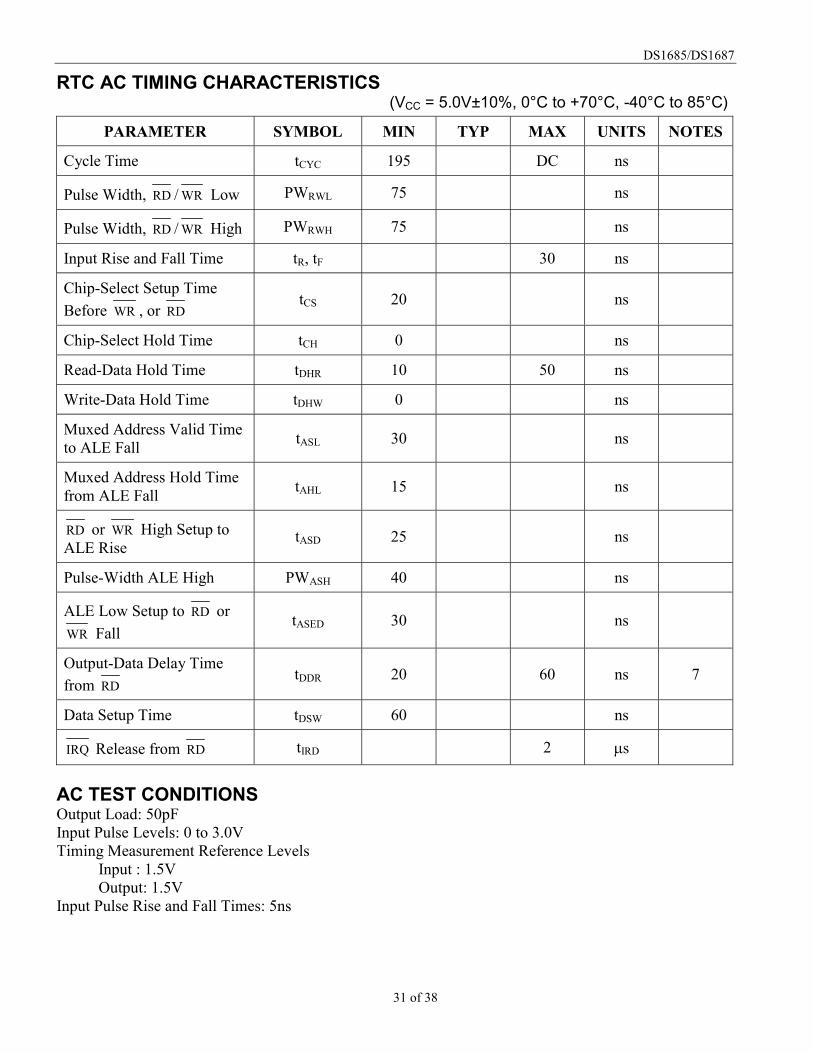
RTC AC TIMING CHARACTERISTICS (VCC = 5.0V±10%, 0°C to +70°C, -40°C to 85°C)
PARAMETER SYMBOL MIN TYP MAX UNITS NOTES
Cycle Time tCYC 195 DC ns
Pulse Width, RD / WR Low PWRWL 75 ns
Pulse Width, RD / WR High PWRWH 75 ns
Input Rise and Fall Time tR, tF 30 ns
Chip-Select Setup TimeBefore WR , or RD
tCS 20 ns
Chip-Select Hold Time tCH 0 ns
Read-Data Hold Time tDHR 10 50 ns
Write-Data Hold Time tDHW 0 ns
Muxed Address Valid Timeto ALE Fall tASL 30 ns
Muxed Address Hold Timefrom ALE Fall tAHL 15 ns
RD or WR High Setup toALE Rise
tASD 25 ns
Pulse-Width ALE High PWASH 40 ns
ALE Low Setup to RD orWR Fall
tASED 30 ns
Output-Data Delay Timefrom RD
tDDR 20 60 ns 7
Data Setup Time tDSW 60 ns
IRQ Release from RD tIRD 2 �s
AC TEST CONDITIONSOutput Load: 50pFInput Pulse Levels: 0 to 3.0VTiming Measurement Reference Levels
Input : 1.5VOutput: 1.5V
Input Pulse Rise and Fall Times: 5ns
DS1685/DS1687
32 of 38
DS1685/DS1667 BUS TIMING FOR READ CYCLE TO RTC AND RTCREGISTERS
DS1685/DS1687 BUS TIMING FOR WRITE CYCLE TO RTC AND RTCREGISTERS
DS1685/DS1687
33 of 38
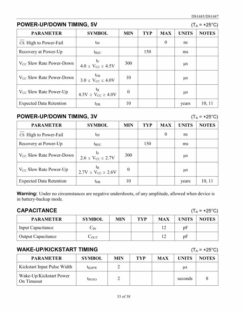
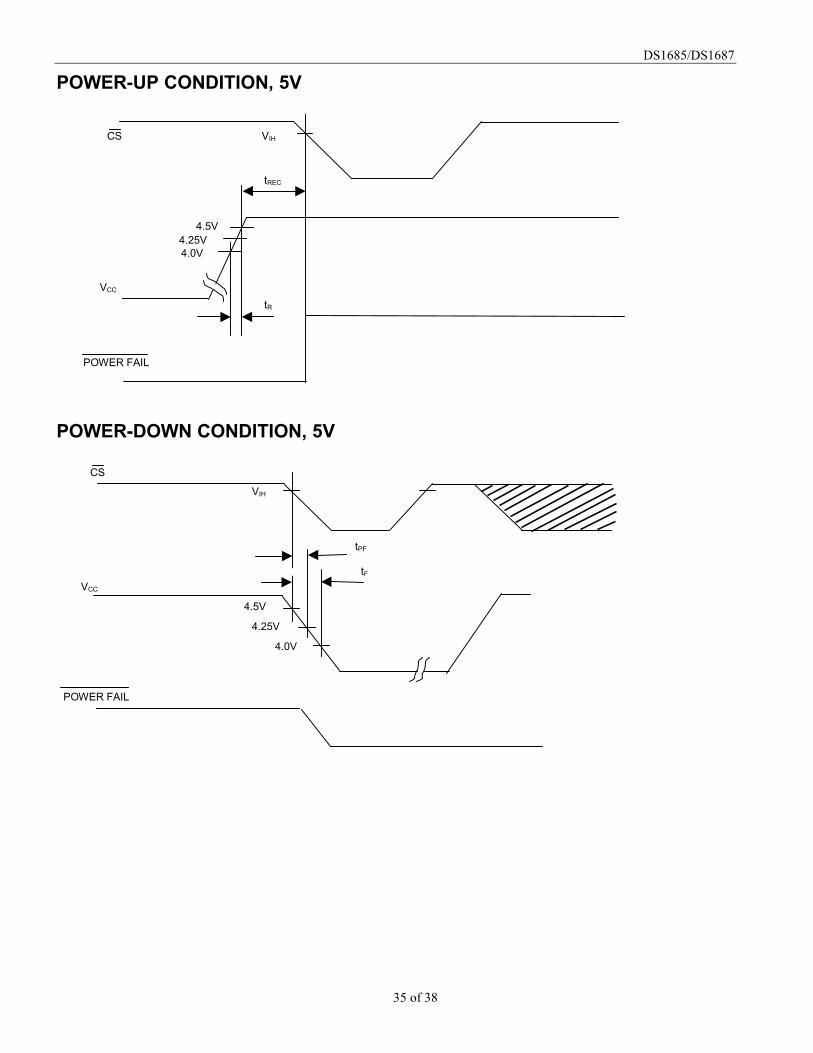
POWER-UP/DOWN TIMING, 5V (TA = +25°C)
PARAMETER SYMBOL MIN TYP MAX UNITS NOTES
CS High to Power-Fail tPF 0 ns
Recovery at Power-Up tREC 150 ms
VCC Slew Rate Power-Down tF4.0 � VCC � 4.5V 300 �s
VCC Slew Rate Power-Down tFB3.0 � VCC � 4.0V 10 �s
VCC Slew Rate Power-Up tR4.5V � VCC � 4.0V 0 �s
Expected Data Retention tDR 10 years 10, 11
POWER-UP/DOWN TIMING, 3V (TA = +25°C)
PARAMETER SYMBOL MIN TYP MAX UNITS NOTES
CS High to Power-Fail tPF 0 ns
Recovery at Power-Up tREC 150 ms
VCC Slew Rate Power-Down tF2.6 � VCC � 2.7V 300 �s
VCC Slew Rate Power-Up tR2.7V � VCC � 2.6V 0 �s
Expected Data Retention tDR 10 years 10, 11
Warning: Under no circumstances are negative undershoots, of any amplitude, allowed when device isin battery-backup mode.
CAPACITANCE (TA = +25°C)
PARAMETER SYMBOL MIN TYP MAX UNITS NOTES
Input Capacitance CIN 12 pF
Output Capacitance COUT 12 pF
WAKE-UP/KICKSTART TIMING (TA = +25°C)
PARAMETER SYMBOL MIN TYP MAX UNITS NOTES
Kickstart Input Pulse Width tKSPW 2 �s
Wake-Up/Kickstart PowerOn Timeout tPOTO 2 seconds 8
DS1685/DS1687
34 of 38
POWER-UP CONDITION, 3V
POWER-DOWN CONDITION, 3V
CS VIH
tREC
2.7V2.6V2.5V
VCC
POWER FAIL
tR
CS
POWER FAIL
VCC
VIH
tPF
tF
2.7V
2.6V
2.5V
DS1685/DS1687
35 of 38
POWER-UP CONDITION, 5V
POWER-DOWN CONDITION, 5V
CS VIH
tREC
4.5V4.25V4.0V
VCC
POWER FAIL
tR
POWER FAIL
VCC
CS
VIH
tPF
tF
4.5V
4.25V
4.0V
DS1685/DS1687
36 of 38
WAKE-UP/KICKSTART TIMING
*This condition can occur with the 3V device.
Note: Time intervals shown above are referenced in Wake-Up/Kickstart section.
DS1685/DS1687
37 of 38
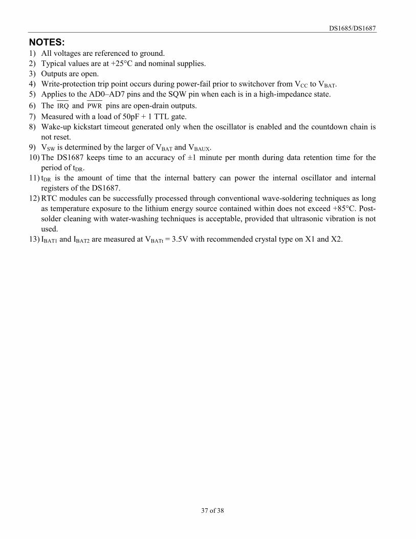
NOTES:1) All voltages are referenced to ground.2) Typical values are at +25°C and nominal supplies.3) Outputs are open.4) Write-protection trip point occurs during power-fail prior to switchover from VCC to VBAT.5) Applies to the AD0–AD7 pins and the SQW pin when each is in a high-impedance state.6) The IRQ and PWR pins are open-drain outputs.7) Measured with a load of 50pF + 1 TTL gate.8) Wake-up kickstart timeout generated only when the oscillator is enabled and the countdown chain is
not reset.9) VSW is determined by the larger of VBAT and VBAUX.10) The DS1687 keeps time to an accuracy of ±1 minute per month during data retention time for the
period of tDR.11) tDR is the amount of time that the internal battery can power the internal oscillator and internal
registers of the DS1687.12) RTC modules can be successfully processed through conventional wave-soldering techniques as long
as temperature exposure to the lithium energy source contained within does not exceed +85°C. Post-solder cleaning with water-washing techniques is acceptable, provided that ultrasonic vibration is notused.
13) IBAT1 and IBAT2 are measured at VBATt = 3.5V with recommended crystal type on X1 and X2.
DS1685/DS1687
38 of 38
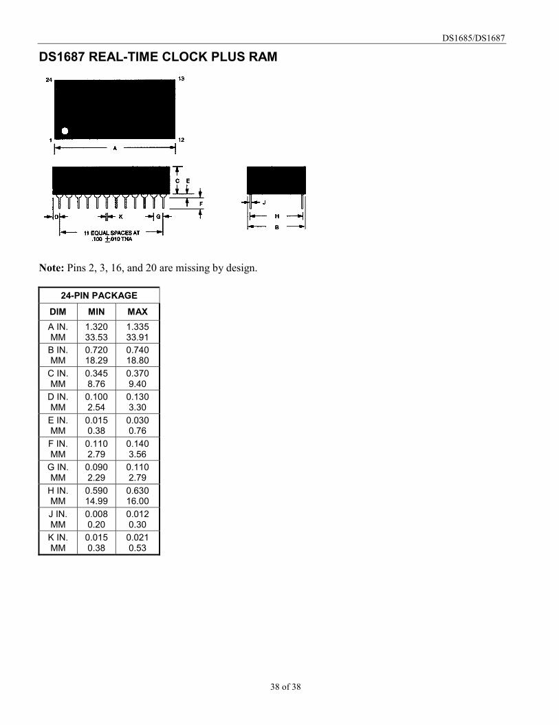
DS1687 REAL-TIME CLOCK PLUS RAM
Note: Pins 2, 3, 16, and 20 are missing by design.
24-PIN PACKAGEDIM MIN MAXA IN.MM
1.32033.53
1.33533.91
B IN.MM
0.72018.29
0.74018.80
C IN.MM
0.3458.76
0.3709.40
D IN.MM
0.1002.54
0.1303.30
E IN.MM
0.0150.38
0.0300.76
F IN.MM
0.1102.79
0.1403.56
G IN.MM
0.0902.29
0.1102.79
H IN.MM
0.59014.99
0.63016.00
J IN.MM
0.0080.20
0.0120.30
K IN.MM
0.0150.38
0.0210.53


![GENRAL WIRING (GENRAL WIRING-1) · sdcd vdd(3r3v) sddat0 sd board gnd gnd gnd 3r3v 3r3v gnd maindak maindbk 5v [main dial] pbabk gnd pbbbk pclek pbbak rfl 3r3v 3r3v gnd gnd afl phoe](https://img.pdfslide.us/doc/110x75/5c000ba809d3f2c9268ca1e5/genral-wiring-genral-wiring-1-sdcd-vdd3r3v-sddat0-sd-board-gnd-gnd-gnd-3r3v.jpg)


![Wireless Starter Kit Mainboard - Silicon Labs · vcom_enable pti0[0..2] vmcu gnd gnd gnd gnd vmcu vrf 5v 3v3 gnd vrf gnd gnd gnd gnd gnd usb_vbus usb_vreg usb_vbus 5v 5v_dbg …](https://img.pdfslide.us/doc/110x75/5ac0fbea7f8b9a4e7c8c7c14/wireless-starter-kit-mainboard-silicon-labs-pti002-vmcu-gnd-gnd-gnd-gnd-vmcu.jpg)