Embed Size (px)
Citation preview

8V to 38 V
DRV8816
Brushed DC Motor Driver BDC
EN / IN42.8A peak
nSLEEP
nFAULT
VPROPI
Controller
Protection
Product
Folder
Sample &Buy
Technical
Documents
Tools &
Software
Support &Community
An IMPORTANT NOTICE at the end of this data sheet addresses availability, warranty, changes, use in safety-critical applications,intellectual property matters and other important disclaimers. PRODUCTION DATA.
DRV8816SLRS063C –SEPTEMBER 2013–REVISED FEBRUARY 2016
DRV8816 DMOS Dual 1/2-H-Bridge Motor Drivers
1
1 Features1• H-Bridge Motor Driver Individual
– Drives a DC Motor or Other Loads– Low RDS(on) MOSFETs (0.4-Ω TYP)
• Low-Power Sleep Mode• 100% PWM Supported• 8- to 38-V Operating Supply Voltage Range• Thermally Enhanced Surface Mount Package• Configurable Overcurrent Limit• Protection Features
– VBB Undervoltage Lockout (UVLO)– Charge Pump Undervoltage (CPUV)– Overcurrent Protection (OCP)– Short-to-Supply Protection (STS)– Short-to-Ground Protection (STG)– Overtemperature Warning (OTW)– Overtemperature Shutdown (OTS)– Fault Condition Indication Pin (nFAULT)
2 Applications• Printers• Industrial Automation• Robotics• Motorized Levers
3 DescriptionThe DRV8816 provides a versatile power driversolution with two independent ½-H bridge drivers.The device can drive one brushed DC motor or onewinding of a stepper motor, as well as other deviceslike solenoids. A simple INx/ENx interface allowseasy interfacing to controller circuits.
The output stages use N-channel power MOSFETsconfigured as ½-H-bridges. The DRV8816 is capableof peak output currents up to ±2.8 A and operatingvoltages up to 38 V. An internal charge pumpgenerates needed gate drive voltages.
A low-power sleep mode is provided which shutsdown internal circuitry to achieve very-low quiescentcurrent draw. This sleep mode can be set using adedicated nSLEEP pin.
Internal protection functions are provided for UVLO,charge pump fault, OCP, short-to-supply protection,short-to-ground protection, overtemperature warning,and overtemperature shutdown. Fault conditions areindicated through a nFAULT pin
The DRV8816 is packaged in a 16-pin HTSSOPpackage with PowerPAD™ (Eco-friendly: RoHS & noSb/Br)
Device Information(1)
PART NUMBER PACKAGE BODY SIZE (NOM)DRV8816 HTSSOP (16) 4.40 mm × 5.00 mm
(1) For all available packages, see the orderable addendum atthe end of the data sheet.
Simplified Schematic

2
DRV8816SLRS063C –SEPTEMBER 2013–REVISED FEBRUARY 2016 www.ti.com
Product Folder Links: DRV8816
Submit Documentation Feedback Copyright © 2013–2016, Texas Instruments Incorporated
Table of Contents1 Features .................................................................. 12 Applications ........................................................... 13 Description ............................................................. 14 Revision History..................................................... 25 Pin Configuration and Functions ......................... 36 Specifications......................................................... 4
6.1 Absolute Maximum Ratings ...................................... 46.2 ESD Ratings.............................................................. 46.3 Recommended Operating Conditions ...................... 46.4 Thermal Information .................................................. 56.5 Electrical Characteristics........................................... 56.6 Typical Characteristics .............................................. 6
7 Detailed Description .............................................. 87.1 Overview ................................................................... 87.2 Functional Block Diagram ......................................... 87.3 Feature Description................................................... 87.4 Device Functional Modes........................................ 11
8 Application and Implementation ........................ 138.1 Application Information............................................ 138.2 Typical Application ................................................. 13
9 Power Supply Recommendations ...................... 169.1 Bulk Capacitance .................................................... 169.2 Power Supervisor.................................................... 16
10 Layout................................................................... 1710.1 Layout Guidelines ................................................. 1710.2 Layout Example .................................................... 1810.3 Thermal Protection................................................ 18
11 Device and Documentation Support ................. 1911.1 Documentation Support ........................................ 1911.2 Community Resource............................................ 1911.3 Trademarks ........................................................... 1911.4 Electrostatic Discharge Caution............................ 1911.5 Glossary ................................................................ 19
12 Mechanical, Packaging, and OrderableInformation ........................................................... 19
4 Revision HistoryNOTE: Page numbers for previous revisions may differ from page numbers in the current version.
Changes from Revision B (October 2014) to Revision C Page
• Updated description for nFAULT pin. .................................................................................................................................... 3• Removed the RVPROPI component........................................................................................................................................... 3• Changed the Functional Block Diagram image ...................................................................................................................... 8• Changed the Typical Application image ............................................................................................................................... 13• Changed the Layout Example image ................................................................................................................................... 18
Changes from Original (September 2013) to Revision A Page
• Added Handling Rating table, Feature Description section, Device Functional Modes, Application andImplementation section, Power Supply Recommendations section, Layout section, Device and DocumentationSupport section, and Mechanical, Packaging, and Orderable Information section ............................................................... 4
• Updated Figure 5.................................................................................................................................................................. 12

1 16 IN2nFAULT
2EN2
3IN1
4GND
5nSLEEP
6
OUT1 7
SENSE 8
15 VPROPI
14 VCP
13 GND
12 CP2
11 CP1
10 OUT2
9 VBB
Pow
erPAD
-G
ND
EN1
3
DRV8816www.ti.com SLRS063C –SEPTEMBER 2013–REVISED FEBRUARY 2016
Product Folder Links: DRV8816
Submit Documentation FeedbackCopyright © 2013–2016, Texas Instruments Incorporated
5 Pin Configuration and Functions
Pin FunctionsPIN
TYPE DESCRIPTIONNAME NO.
POWER AND GROUNDCP1 11 PWR
Charge pump switching node Connect a 0.1-µF X7R capacitor rated for VBB between CP1 and CP2CP2 12 —
GND 4, 13,PPAD PWR Device ground Connect to system ground
VBB 9 PWR Power supply input Connect to main power supply. Bypass to GND with a 0.1-µF ceramiccapacitor and a larger bulk capacitor rated for at least the VBB voltage
VCP 14 PWR Charge pump output Connect a 0.1-µF 16-V ceramic capacitor between VCP and VBBCONTROL
EN1 6I ½-H bridge enable Logic high enables ½-H bridge output; logic low puts the FETs in HI-Z;
internal pull-downEN2 2IN1 3
I ½-H bridge control Logic high enables the high-side ½-H bridge FET; logic low enablesthe low side FET; internal pull-downIN2 16
nFAULT 1 O Fault indication pin Pulled logic low with fault condition; open-drain output requires anexternal pull-up. This output is indeterminate in sleep mode
nSLEEP 5 I Device sleep mode Pull logic low to put device into a low-power sleep mode; internal pull-down
OUTPUTOUT1 7 O ½-H bridge outputOUT2 10 O ½-H bridge output
SENSE 8 O H-bridge low-side connect Connect directly to GND or through a sense resistor to set OCPVPROPIVPROPI 15 O Current-proportional output
(1) VCC is not a pin on the DRV8816, but a VCC supply voltage pullup is required.
Table 1. External ComponentsCOMPONENT PIN 1 PIN 2 RECOMMENDED
CVBB VBB GND 0.1-µF ceramic capacitor and a larger bulk capacitor rated for at least the VBBvoltage
CVCP VCP VBB 0.1-µF 16-V ceramic capacitorRnFAULT VCC (1) nFAULT >1 kΩ resistorRnSLEEP VCC (1) nSLEEP If nSLEEP isn't actively controlled, use a pull-up resistor of less than 20 kΩRSENSE SENSE GND Optional low-value resistor. If not used, connect SENSE pin directly to GND.

4
DRV8816SLRS063C –SEPTEMBER 2013–REVISED FEBRUARY 2016 www.ti.com
Product Folder Links: DRV8816
Submit Documentation Feedback Copyright © 2013–2016, Texas Instruments Incorporated
(1) Stresses beyond those listed under Absolute Maximum Ratings may cause permanent damage to the device. These are stress ratingsonly, which do not imply functional operation of the device at these or any other conditions beyond those indicated under RecommendedOperating Conditions. Exposure to absolute-maximum-rated conditions for extended periods may affect device reliability.
(2) Transients of ±1 V for less than 25 ns are acceptable.
6 Specifications
6.1 Absolute Maximum Ratingsover operating free-air temperature range (unless otherwise noted) (1)
MIN MAX UNITVBB Power supply voltage –0.6 40 V
Charge pump positive switching pin (CP2) –0.6 VBB + 7 VCharge pump negative switching pin (CP1) –0.6 VBB VDigital pin voltage range (IN1, IN2, EN1, EN2, nSLEEP, nFAULT) –0.3 7 VVBB to OUTx –0.6 40 VOUTx to SENSE –0.6 40 V
V(SENSE) Sense voltage (SENSE) (2) –0.5 1.0 VH-bridge output current (OUT1, OUT2, SENSE) 0 2.8 AVPROPI pin voltage range (VPROPI) –0.3 3.6 V
TA Operating ambient temperature –40 85 °CTJ Operating junction temperature –40 190 °CTstg Storage temperature –40 125 °C
(1) JEDEC document JEP155 states that 500-V HBM allows safe manufacturing with a standard ESD control process(2) JEDEC document JEP157 states that 250-V CDM allows safe manufacturing with a standard ESD control process.
6.2 ESD RatingsVALUE UNIT
V(ESD) Electrostatic dischargeHuman-body model (HBM), per ANSI/ESDA/JEDEC JS-001 (1) ±2000
VCharged-device model (CDM), per JEDEC specification JESD22-C101 (2) ±500
6.3 Recommended Operating ConditionsPower dissipation and thermal limits must be observed.
MIN MAX UNITVBB Power supply voltage 8 38 VVI Input pin voltage 0 5.5 VfPWM Applied PWM signal (IN1, IN2, EN1, EN2) 100 kHzIOUT H-bridge output current 2.8 ATA Ambient temperature –40 85 °C
5
DRV8816www.ti.com SLRS063C –SEPTEMBER 2013–REVISED FEBRUARY 2016
Product Folder Links: DRV8816
Submit Documentation FeedbackCopyright © 2013–2016, Texas Instruments Incorporated
(1) For more information about traditional and new thermal metrics, see the IC Package Thermal Metrics application report, SPRA953.(2) The junction-to-ambient thermal resistance under natural convection is obtained in a simulation on a JEDEC-standard, high-K board, as
specified in JESD51-7, in an environment described in JESD51-2a.(3) The junction-to-case (top) thermal resistance is obtained by simulating a cold plate test on the package top. No specific JEDEC-
standard test exists, but a close description can be found in the ANSI SEMI standard G30-88.(4) The junction-to-board thermal resistance is obtained by simulating in an environment with a ring cold plate fixture to control the PCB
temperature, as described in JESD51-8.(5) The junction-to-top characterization parameter, ψ JT , estimates the junction temperature of a device in a real system and is extracted
from the simulation data for obtaining θ JA , using a procedure described in JESD51-2a (sections 6 and 7).(6) The junction-to-board characterization parameter, ψ JB , estimates the junction temperature of a device in a real system and is extracted
from the simulation data for obtaining θ JA , using a procedure described in JESD51-2a (sections 6 and 7).(7) The junction-to-case (bottom) thermal resistance is obtained by simulating a cold plate test on the exposed (power) pad. No specific
JEDEC standard test exists, but a close description can be found in the ANSI SEMI standard G30-88.
6.4 Thermal Information
THERMAL METRIC (1)DRV8816
UNITPWP (HTSSOP)16 PINS
RθJA Junction-to-ambient thermal resistance (2) 43.9 °C/WRθJC(top) Junction-to-case (top) thermal resistance (3) 30.8 °C/WRθJB Junction-to-board thermal resistance (4) 25.3 °C/WψJT Junction-to-top characterization parameter (5) 1.1 °C/WψJB Junction-to-board characterization parameter (6) 25 °C/WRθJC(bot) Junction-to-case (bottom) thermal resistance (7) 5.6 °C/W
6.5 Electrical Characteristicsover recommended operating conditions (unless otherwise noted)
PARAMETER TEST CONDITIONS MIN TYP MAX UNITPOWER SUPPLIES (VBB)VBB VBB operating voltage 8 38 V
IVBB VBB operating supply currentƒPWM < 50 kHz 6 mACharge pump on, Outputs disabled 3.2 mA
IVBBQ VBB sleep-mode supply current nSLEEP = 0, TJ = 25°C 10 µACONTROL INPUTS (IN1, IN2, EN1, EN2, nSLEEP)VIL Input logic low voltage IN1, IN2, EN1, EN2 0 0.8 VVIH Input logic high voltage IN1, IN2, EN1, EN2 2 5.5 VVIL Input logic low voltage nSLEEP 0 0.8 VVIH Input logic high voltage nSLEEP 2.2 5.5 VIIL Input logic low current IN1, IN2, EN2, nSLEEP VIN = 0 V 0 μAIIH Input logic high current IN1, IN2, EN2, nSLEEP VIN = 5 V 25 μAIIL Input logic low current EN1 VIN = 0 V 0 μAIIH Input logic high current EN1 VIN = 5 V 100 μA
RPD Pulldown resistanceIN1, IN2, EN2, nSLEEP 200
kΩEN1 50
SERIAL AND CONTROL OUTPUT (nFAULT)VOL Output logic low voltage Isink = 1 mA 0.4 VDMOS DRIVERS (OUT1, OUT2, SENSE)
RDS(on) Output ON resistance
Source driver, IOUT = –2.8 A, TJ = 25°C 0.48
ΩSource driver, IOUT = –2.8 A, TJ = 125°C 0.74 0.85Sink driver, IOUT = –2.8 A, TJ = 25°C 0.35Sink driver, IOUT = –2.8 A, TJ = 125°C 0.52 0.7
VTRIP SENSE trip voltage RSENSE between SENSE and GND 500 mV
Vf Body diode forward voltageSource diode, If = –2.8 A 1.4
VSink diode, If = 2.8 A 1.4

0
1
2
3
4
5
6
7
8
9
10
8 V 32 V 38 V
Qui
esce
nt C
urre
nt (
µA
)
Supply Voltage
±40C
25°C
125°C
C001
0.86
0.88
0.90
0.92
0.94
0.96
0.98
1.00
1.02
8V 32V
RD
S(O
N) (n
orm
aliz
ed)
Supply Voltage
Source Driver
Sink Driver
C002
6
DRV8816SLRS063C –SEPTEMBER 2013–REVISED FEBRUARY 2016 www.ti.com
Product Folder Links: DRV8816
Submit Documentation Feedback Copyright © 2013–2016, Texas Instruments Incorporated
Electrical Characteristics (continued)over recommended operating conditions (unless otherwise noted)
PARAMETER TEST CONDITIONS MIN TYP MAX UNIT
(1) If OUT2 is High, the typical time for OUT1 to go from High-Z to Low is 1700 ns.(2) Whenever VCP is less than VM + 10 V, a CPUV event occurs. This fault will be asserted whenever VBB is below 12 V. Note that the H-
bridges will remain enabled until VBB = VUVLO even through nFAULT is pulled low.
tpd OUTx propagation delay
From High-Z to High 70
ns
From High-Z to Low 700 (1)
From High to High-Z 120From High to Low 700From Low to High-Z 350From Low to High 350
tCOD Crossover delay 500 nsDAGain VPROPI amplifier gain Sense = 0.1 to 0.4 V 5 V/VPROTECTION CIRCUITSVUVLO VBB UVLO VBB rising 6.5 7.5 VVCPUV VCP UVLO (2) VBB rising; CPUV recovery 12 13.8 VIOCP Overcurrent protection trip level 3 AtDEG Overcurrent deglitch time 3.0 µstOCP Overcurrent retry time 1.6 msTOTW Thermal warning temperature Die temperature Tj 160 °CTOTW HYS Thermal warning hysteresis Die temperature Tj 15 °CTOTS Thermal shutdown temperature Die temperature Tj 175 °CTOTS HYS Thermal shutdown hysteresis Die temperature Tj 15 °C
6.6 Typical Characteristics
Figure 1. IVBBQ vs VBB Figure 2. RDS(ON) vs VBB (normalized to VBB = 8V)

0
10
20
30
40
50
60
5 V 15 V 25 V 35 V 45 V
Cha
rge
Pum
p V
olta
ge (
V)
Supply Voltage C003
7
DRV8816www.ti.com SLRS063C –SEPTEMBER 2013–REVISED FEBRUARY 2016
Product Folder Links: DRV8816
Submit Documentation FeedbackCopyright © 2013–2016, Texas Instruments Incorporated
Typical Characteristics (continued)
Figure 3. VCP vs VBB

Outputs
Power
0.1µFCharge Pump
OUT1
VBB
Pre-driver
VCP
OUT2
VBB
Pre-driver
VCPBDC
VCP
CP1
CP2
VBB
0.1µF0.1µFbulk
SENSE
VPROPI
GND
GND
PPAD
VCP
VBB
Regulators
RSENSE
IN1
IN2
EN1
EN2
nSLEEP
nFAULT
CoreLogic
Protection
Temperature Sensor
Overcurrent Monitoring
Voltage Monitoring
Inputs
5x
8
DRV8816SLRS063C –SEPTEMBER 2013–REVISED FEBRUARY 2016 www.ti.com
Product Folder Links: DRV8816
Submit Documentation Feedback Copyright © 2013–2016, Texas Instruments Incorporated
7 Detailed Description
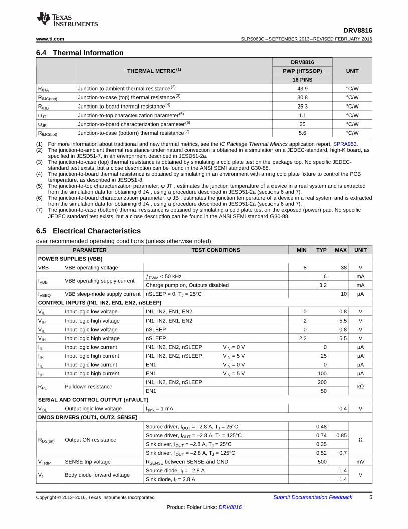
7.1 OverviewThe DRV8816 uses 4 CMOS inputs to control 2 high-voltage high-current outputs, while integrating protectionfeatures, fault reporting, a sleep mode, and current sensing. EN1 and IN1 control OUT1, and EN2 and IN2control OUT2, according to Table 2. The device is designed to drive two independent loads or one brushed DCmotor, as shown in Figure 4 and Table 3.
When an RSENSE resistor is used, the DRV8816 will automatically disable itself if VSENSE exceeds 500mV—thisprovides a user-programmable overcurrent threshold. The VPROPI output equals the sense voltage amplified bya factor of 5, and it can be used by a microcontroller to know the motor current, in order to Pulse-Width Modulatethe DRV8816 inputs and regulate motor current.
7.2 Functional Block Diagram
7.3 Feature Description
7.3.1 Bridge ControlThe DRV8816 is controlled using separate enable and input pins for each ½-H-bridge.
OUT1
OUT2
BDC
OUT1
OUT2
BDC
BDC
OUT1
OUT2
BDC
VBB
BDC
VBB
9
DRV8816www.ti.com SLRS063C –SEPTEMBER 2013–REVISED FEBRUARY 2016
Product Folder Links: DRV8816
Submit Documentation FeedbackCopyright © 2013–2016, Texas Instruments Incorporated
Feature Description (continued)Table 2 shows the logic for the DRV8816.
Table 2. DRV8816 LogicENx INx OUTx
0 X Z1 0 L1 1 H
If a single DC motor is connected to the DRV8816, it is connected between the OUT1 and OUT2 pins as shownin Figure 4. Two DC motors may also be connected to the DRV8816. In this mode, it is not possible to reversethe direction of the motors; the motors will turn only in one direction. The connections are shown in Figure 4.
Figure 4. Bridge Control
Table 3 shows how motor operation for a single-brushed DC motor is controlled.
(1) The Half-H bridges are independent; output state depends on ENx and INx.
Table 3. Motor Operation for a Single-Brushed DC MotorEN1 EN2 IN1 IN2 OUT1 OUT2 Operation
0 X X X Z X (1) Off (coast)X 0 X X X (1) Z Off (coast)1 1 0 0 L L Brake1 1 0 1 L H Reverse1 1 1 0 H L Forward1 1 1 1 H H Brake
Table 4 shows how motor operation for dual-brushed DC motors is controlled.
Table 4. Motor Operation for a Dual-Brushed DC Motor
Motor connected toGND
ENx INx OUTx Operation0 X Z Off (coast)1 0 L Brake1 1 H Forward
Motor connected toVBB
ENx INx OUTx Operation0 X Z Off (coast)1 0 L Forward1 1 H Brake

VBB
VCP
CP1
CP2
VMCharge
Pump
0.1 µF
0.1 µF
10
DRV8816SLRS063C –SEPTEMBER 2013–REVISED FEBRUARY 2016 www.ti.com
Product Folder Links: DRV8816
Submit Documentation Feedback Copyright © 2013–2016, Texas Instruments Incorporated
7.3.2 Charge PumpThe charge pump is used to generate a supply above VBB to drive the source-side DMOS gates. A 0.1-μFceramic monolithic capacitor should be connected between CP1 and CP2 for pumping purposes. A 0.1-μFceramic monolithic capacitor should be connected between VCP and VBB to act as a reservoir to run the high-side DMOS devices. The VCP voltage level is internally monitored, and in the case of a fault condition, theoutputs of the device are disabled.
Figure 5. Charge Pump
7.3.3 VPROPIThe VPROPI output is equal to approximately 5× the voltage present on the SENSE pin. VPROPI is meaningfulonly if there is a resistor connected to the SENSE pin; If SENSE is connected to ground, VPROPI measures 0 V.Also note that during slow decay (brake), VPROPI measures 0 V. VPROPI can output a maximum of 2.5 V,because at 500 mV on SENSE, the H-bridge is disabled.
7.3.4 Protection CircuitsThe DRV8816 is fully protected against VBB undervoltage, charge pump undervoltage, overcurrent, andovertemperature events.
7.3.4.1 VBB UVLOIf at any time the voltage on the VBB pin falls below the UVLO threshold voltage, all FETs in the H-bridge will bedisabled and the charge pump will be disabled. Operation will resume when VBB rises above the UVLOthreshold. Note that nFAULT does not indicate a UVLO because the CPUV fault is always asserted below VBB =12 V.
7.3.4.2 VCP UVLO (CPUV)During a CPUV event, the VCP voltage is measured to be below VCP + 10 V. If at any time the voltage on theVCP pin falls below the UVLO threshold voltage, the nFAULT pin is driven low. The nFAULT pin is released afteroperation has resumed. Note that this fault does not disable the output FETs and allows the device to continueoperating. When VBB is below 12 V, this fault condition is always asserted and nFAULT is pulled low.

11
DRV8816www.ti.com SLRS063C –SEPTEMBER 2013–REVISED FEBRUARY 2016
Product Folder Links: DRV8816
Submit Documentation FeedbackCopyright © 2013–2016, Texas Instruments Incorporated
7.3.4.3 OCPThe current flowing through the high-side and low-side drivers is monitored to ensure that the motor lead is notshorted to supply or ground. If a short is detected, all FETs in the H-bridge are disabled, nFAULT is driven low,and a tOCP fault timer is started. After this period, tOCP, the device is then allowed to follow the input commandsand another turn-on is attempted (nFAULT becomes high again during this attempt). If there is still a faultcondition, the cycle repeats. If after tOCP expires it is determined the short condition is not present, normaloperation resumes and nFAULT is released.
7.3.4.4 OTWIf the die temperature increases past the thermal warning threshold, the nFAULT pin is driven low. After the dietemperature has fallen below the hysteresis level, the nFAULT pin is released. If the die temperature continues toincrease, the device enters overtemperature shutdown as described in OTS .
7.3.4.5 OTSIf the die temperature exceeds safe limits, all FETs in the H-bridge are disabled and the charge pump is shutdown. After the die temperature has fallen to a safe level, operation automatically resumes.
7.4 Device Functional Modes
7.4.1 SENSEA low-value resistor can be placed between the SENSE pin and ground for current-sensing purposes. The PCBshould be designed with wide metal paths on each side of the resistor, to minimize IR drop that would decreasesense accuracy. Likewise, the distance from the sense resistor to the DRV8816 and bulk capacitor should beminimized.
To set a manual overcurrent trip threshold, place a resistor between the SENSE pin and GND. When the SENSEpin rises above 500 mV, the H-bridge output is disabled (High-Z). The device will automatically retry with a periodof tOCP. The overcurrent trip threshold can be calculated using ITRIP = 500 mV/Ω. The overcurrent trip levelselected cannot be greater than IOCP.
If a sense resistor is not used, tie the SENSE pin directly to GND; in that case, the IOCP detection of currentthrough the internal FETs still functions.

tOCPtDEG
IPEAK
IOCP
IOUTx
High-ZVOUT+
VOUT-
Enable,
Source
or Sink
nFAULT
Motor Lead
Short Condition
Normal DC
No Fault Condition
12
DRV8816SLRS063C –SEPTEMBER 2013–REVISED FEBRUARY 2016 www.ti.com
Product Folder Links: DRV8816
Submit Documentation Feedback Copyright © 2013–2016, Texas Instruments Incorporated
Device Functional Modes (continued)
Figure 6. Overcurrent Threshold
ControllerEN2
IN1
GND
nFAULT
nSLEEP
EN1
OUT1
SENSE
VPROPI
VCP
GND
IN2
OUT2
VBB
0.1µFCP2
CP1
0.25 100µF0.1µF
DRV8816
ADC
PU
+±
8V - 38VPower Supply
BDC
0.1µF
PPAD
optionalRC filter
13
DRV8816www.ti.com SLRS063C –SEPTEMBER 2013–REVISED FEBRUARY 2016
Product Folder Links: DRV8816
Submit Documentation FeedbackCopyright © 2013–2016, Texas Instruments Incorporated
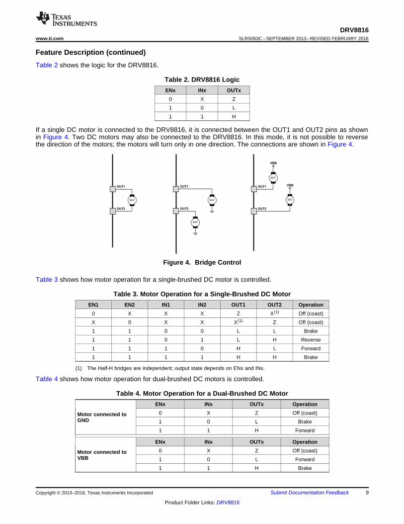
8 Application and Implementation
NOTEInformation in the following applications sections is not part of the TI componentspecification, and TI does not warrant its accuracy or completeness. TI’s customers areresponsible for determining suitability of components for their purposes. Customers shouldvalidate and test their design implementation to confirm system functionality.
8.1 Application InformationThe DRV8816 is typically used to drive a brushed DC motor.
8.2 Typical Application
Figure 7. Typical Application
8.2.1 Design RequirementsTable 5 shows parameters to consider when designing.
Table 5. Design ParametersDESIGN PARAMETER REFERENCE EXAMPLE VALUE
Motor voltage VBB 24 VMotor RMS current IRMS 0.8 A
Motor startup current ISTART 2 AMotor current trip point ITRIP 2.5 A
SENSE TRIPR = 0.5V / I
2
RMS DS(ON) DS(ON)Power I (High-Side R + Low-Side R )» ´
14
DRV8816SLRS063C –SEPTEMBER 2013–REVISED FEBRUARY 2016 www.ti.com
Product Folder Links: DRV8816
Submit Documentation Feedback Copyright © 2013–2016, Texas Instruments Incorporated
8.2.2 Detailed Design Procedure
8.2.2.1 Motor VoltageThe motor voltage to use will depend on the ratings of the motor selected and the desired RPM. A higher voltagespins a brushed DC motor faster with the same PWM duty cycle applied to the power FETs. A higher voltagealso increases the rate of current change through the inductive motor windings.
8.2.2.2 Power DissipationThe power dissipation of the DRV8816 is a function of RMS motor current and the each output’s FET resistance(RDS(ON)).
(1)
For this example, the ambient temperature is 35°C, and the junction temperature reaches 65°C. At 65°C, thesum of RDS(ON) is about 1Ω. With an example motor current of 0.8A, the dissipated power in the form of heat willbe 0.8A² x 1Ω = 0.64W.
The temperature that the DRV8816 reaches will depend on the thermal resistance to the air and PCB. It isimportant to solder the device PowerPAD to the PCB ground plane, with vias to the top and bottom board layers,in order dissipate heat into the PCB and reduce the device temperature. In the example used here, the DRV8816had an effective thermal resistance RθJA of 47°C/W, and:
(2)
8.2.2.3 Motor Current Trip PointWhen the voltage on pin SENSE exceeds VTRIP (0.5V), overcurrent is detected. The RSENSE resistor should besized to set the desired ITRIP level.
(3)
To set ITRIP to 2A, RSENSE = 0.5V / 2A = 0.25Ω.
To prevent false trips, ITRIP must be higher than regular operating current. Motor current during startup is typicallymuch higher than steady-state spinning, because the initial load torque is higher, and the absence of back-EMFcauses a higher voltage and extra current across the motor windings.
It can be beneficial to limit startup current by using series inductors on the DRV8816 output, as that allows ITRIPto be lower, and it may decrease the system’s required bulk capacitance. Startup current can also be limited byramping the forward drive duty cycle.
8.2.2.4 Sense Resistor SelectionFor optimal performance, it is important for the sense resistor to be:• Surface-mount• Low inductance• Rated for high enough power• Placed closely to the motor driver
The power dissipated by the sense resistor equals IRMS² x R. For example, if peak motor current is 3A, RMSmotor current is 2A, and a 0.05Ω sense resistor is used, the resistor will dissipate 2A² x 0.05Ω = 0.2W. Thepower quickly increases with higher current levels.
Resistors typically have a rated power within some ambient temperature range, along with a de-rated powercurve for high ambient temperatures. When a PCB is shared with other components generating heat, marginshould be added. It is always best to measure the actual sense resistor temperature in a final system, along withthe power MOSFETs, as those are often the hottest components.
Because power resistors are larger and more expensive than standard resistors, it is common practice to usemultiple standard resistors in parallel, between the sense node and ground. This distributes the current and heatdissipation.

15
DRV8816www.ti.com SLRS063C –SEPTEMBER 2013–REVISED FEBRUARY 2016
Product Folder Links: DRV8816
Submit Documentation FeedbackCopyright © 2013–2016, Texas Instruments Incorporated
8.2.3 Application Curves
Figure 8. Forward Drive, Fast Decay Figure 9. Reverse Drive, Fast Decay
Figure 10. Forward Drive, Slow Decay Figure 11. Reverse Drive, Slow Decay

Local Bulk Capacitor
Parasitic WireInductance
+±
Motor Driver
Power Supply Motor Drive System
VBB
GND
+
IC Bypass Capacitor
16
DRV8816SLRS063C –SEPTEMBER 2013–REVISED FEBRUARY 2016 www.ti.com
Product Folder Links: DRV8816
Submit Documentation Feedback Copyright © 2013–2016, Texas Instruments Incorporated
9 Power Supply Recommendations
9.1 Bulk CapacitanceHaving appropriate local bulk capacitance is an important factor in motor drive system design. It is generallybeneficial to have more bulk capacitance, while the disadvantages are increased cost and physical size.
The amount of local capacitance needed depends on a variety of factors, including:• The highest current required by the motor system.• The power supply's capacitance and ability to source current.• The amount of parasitic inductance between the power supply and motor systems.• The acceptable voltage ripple.• The type of motor used (Brushed DC, Brushless DC, Stepper).• The motor braking method.
The inductance between the power supply and motor drive system will limit the rate current can change from thepower supply. If the local bulk capacitance is too small, the system will respond to excessive current demands ordumps from the motor with a change in voltage. When adequate bulk capacitance is used, the motor voltageremains stable and high current can be quickly supplied.
The datasheet generally provides a recommended value, but system-level testing is required to determine theappropriate sized bulk capacitor.
Figure 12. Example Setup of Motor Drive System with External Power Supply
9.2 Power SupervisorControl input nSLEEP is used to minimize power consumption when the DRV8816 is not in use. This disablesmuch of the internal circuitry, including the internal voltage rails and charge pump. nSLEEP is asserted low. Alogic high on this input pin results in normal operation. When switching from low to high, the user should allow a1-ms delay before applying PWM signals. This time is needed for the charge pump to stabilize.

( ) ( )2
TOT D OS O RMN UT SP I(R )= ´
17
DRV8816www.ti.com SLRS063C –SEPTEMBER 2013–REVISED FEBRUARY 2016
Product Folder Links: DRV8816
Submit Documentation FeedbackCopyright © 2013–2016, Texas Instruments Incorporated
10 Layout
10.1 Layout GuidelinesThe printed circuit board (PCB) should use a heavy ground plane. For optimum electrical and thermalperformance, the DRV8816 must be soldered directly onto the board. On the underside of the DRV8816 is athermal pad, which provides a path for enhanced thermal dissipation. The thermal pad should be soldereddirectly to an exposed surface on the PCB. Thermal vias are used to transfer heat to other layers of the PCB.
The load supply pin, VBB, should be decoupled with an electrolytic capacitor (typically 100 μF) in parallel with aceramic capacitor placed as close as possible to the device. The ceramic capacitors between VCP and VBB,connected to VREG, and between CP1 and CP2 should be as close to the pins of the device as possible, inorder to minimize lead inductance.
where• PTOT is the total power dissipation.• RDS(ON) is the resistance of the HS plus LS FETS.• IOUT(RMS) is the RMS output current being applied to each winding. (4)
The voltage rating for bulk capacitors should be higher than the operating voltage, to provide margin for caseswhen the motor transfers energy to the supply.
IOUT(RMS) is equal to approximately 0.7× the full-scale output current setting.
The maximum amount of power that can be dissipated in the device is dependent on ambient temperature andheatsinking.
Note that RDS(ON) increases with temperature, so as the device heats, the power dissipation increases.
10.1.1 GroundA ground power plane should be located as close to DRV8816 as possible. The copper ground plane directlyunder the thermal pad makes a good location. This pad can then be connected to ground for this purpose.
+
nFAULT
EN2
IN1
GND
nSLEEP
EN1
OUT1
SENSE
IN2
VPROPI
VCP
GND
CP2
CP1
VBB
OUT2
18
DRV8816SLRS063C –SEPTEMBER 2013–REVISED FEBRUARY 2016 www.ti.com
Product Folder Links: DRV8816
Submit Documentation Feedback Copyright © 2013–2016, Texas Instruments Incorporated
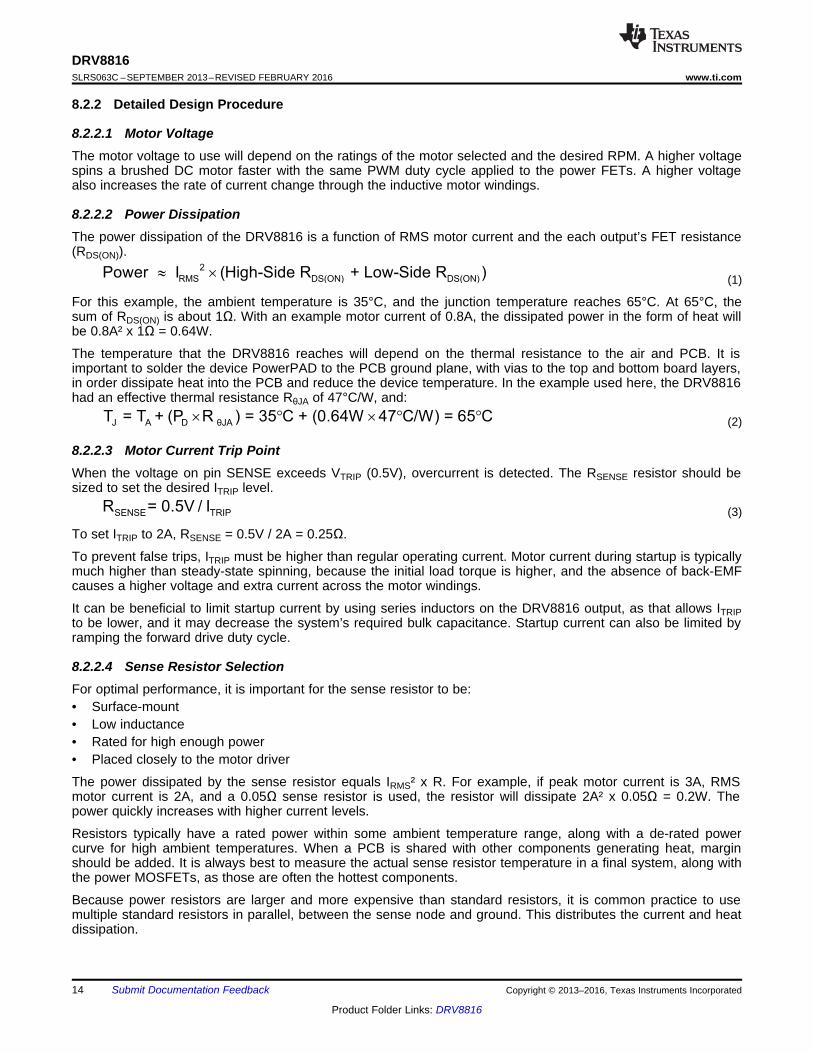
10.2 Layout Example
Figure 13. DRV8816 Layout Example
10.3 Thermal ProtectionIf the die temperature exceeds approximately 150°C, the device is disabled until the temperature drops to a safelevel. Any tendency of the device to enter thermal shutdown is an indication of either excessive powerdissipation, insufficient heatsinking, or too high an ambient temperature.
19
DRV8816www.ti.com SLRS063C –SEPTEMBER 2013–REVISED FEBRUARY 2016
Product Folder Links: DRV8816
Submit Documentation FeedbackCopyright © 2013–2016, Texas Instruments Incorporated
11 Device and Documentation Support
11.1 Documentation Support
11.1.1 Related DocumentationFor related documentation see the following:• DRV8816 Evaluation Module, SLVU971• Shelf-Life Evaluation of Lead-Free Component Finishes, SZZA046
11.2 Community ResourceThe following links connect to TI community resources. Linked contents are provided "AS IS" by the respectivecontributors. They do not constitute TI specifications and do not necessarily reflect TI's views; see TI's Terms ofUse.
TI E2E™ Online Community TI's Engineer-to-Engineer (E2E) Community. Created to foster collaborationamong engineers. At e2e.ti.com, you can ask questions, share knowledge, explore ideas and helpsolve problems with fellow engineers.
Design Support TI's Design Support Quickly find helpful E2E forums along with design support tools andcontact information for technical support.
11.3 TrademarksPowerPAD, E2E are trademarks of Texas Instruments.All other trademarks are the property of their respective owners.
11.4 Electrostatic Discharge CautionThese devices have limited built-in ESD protection. The leads should be shorted together or the device placed in conductive foamduring storage or handling to prevent electrostatic damage to the MOS gates.
11.5 GlossarySLYZ022 — TI Glossary.
This glossary lists and explains terms, acronyms, and definitions.
12 Mechanical, Packaging, and Orderable InformationThe following pages include mechanical, packaging, and orderable information. This information is the mostcurrent data available for the designated devices. This data is subject to change without notice and revision ofthis document. For browser-based versions of this data sheet, refer to the left-hand navigation.

PACKAGE OPTION ADDENDUM
www.ti.com 15-Apr-2015
Addendum-Page 1
PACKAGING INFORMATION
Orderable Device Status(1)
Package Type PackageDrawing
Pins PackageQty
Eco Plan(2)
Lead/Ball Finish(6)
MSL Peak Temp(3)
Op Temp (°C) Device Marking(4/5)
Samples
DRV8816PWP ACTIVE HTSSOP PWP 16 90 Green (RoHS& no Sb/Br)
CU NIPDAU Level-3-260C-168 HR -40 to 85 DRV8816
DRV8816PWPR ACTIVE HTSSOP PWP 16 2000 Green (RoHS& no Sb/Br)
CU NIPDAU Level-3-260C-168 HR -40 to 85 DRV8816
(1) The marketing status values are defined as follows:ACTIVE: Product device recommended for new designs.LIFEBUY: TI has announced that the device will be discontinued, and a lifetime-buy period is in effect.NRND: Not recommended for new designs. Device is in production to support existing customers, but TI does not recommend using this part in a new design.PREVIEW: Device has been announced but is not in production. Samples may or may not be available.OBSOLETE: TI has discontinued the production of the device.
(2) Eco Plan - The planned eco-friendly classification: Pb-Free (RoHS), Pb-Free (RoHS Exempt), or Green (RoHS & no Sb/Br) - please check http://www.ti.com/productcontent for the latest availabilityinformation and additional product content details.TBD: The Pb-Free/Green conversion plan has not been defined.Pb-Free (RoHS): TI's terms "Lead-Free" or "Pb-Free" mean semiconductor products that are compatible with the current RoHS requirements for all 6 substances, including the requirement thatlead not exceed 0.1% by weight in homogeneous materials. Where designed to be soldered at high temperatures, TI Pb-Free products are suitable for use in specified lead-free processes.Pb-Free (RoHS Exempt): This component has a RoHS exemption for either 1) lead-based flip-chip solder bumps used between the die and package, or 2) lead-based die adhesive used betweenthe die and leadframe. The component is otherwise considered Pb-Free (RoHS compatible) as defined above.Green (RoHS & no Sb/Br): TI defines "Green" to mean Pb-Free (RoHS compatible), and free of Bromine (Br) and Antimony (Sb) based flame retardants (Br or Sb do not exceed 0.1% by weightin homogeneous material)
(3) MSL, Peak Temp. - The Moisture Sensitivity Level rating according to the JEDEC industry standard classifications, and peak solder temperature.
(4) There may be additional marking, which relates to the logo, the lot trace code information, or the environmental category on the device.
(5) Multiple Device Markings will be inside parentheses. Only one Device Marking contained in parentheses and separated by a "~" will appear on a device. If a line is indented then it is a continuationof the previous line and the two combined represent the entire Device Marking for that device.
(6) Lead/Ball Finish - Orderable Devices may have multiple material finish options. Finish options are separated by a vertical ruled line. Lead/Ball Finish values may wrap to two lines if the finishvalue exceeds the maximum column width.
Important Information and Disclaimer:The information provided on this page represents TI's knowledge and belief as of the date that it is provided. TI bases its knowledge and belief on informationprovided by third parties, and makes no representation or warranty as to the accuracy of such information. Efforts are underway to better integrate information from third parties. TI has taken andcontinues to take reasonable steps to provide representative and accurate information but may not have conducted destructive testing or chemical analysis on incoming materials and chemicals.TI and TI suppliers consider certain information to be proprietary, and thus CAS numbers and other limited information may not be available for release.

PACKAGE OPTION ADDENDUM
www.ti.com 15-Apr-2015
Addendum-Page 2
In no event shall TI's liability arising out of such information exceed the total purchase price of the TI part(s) at issue in this document sold by TI to Customer on an annual basis.

TAPE AND REEL INFORMATION
*All dimensions are nominal
Device PackageType
PackageDrawing
Pins SPQ ReelDiameter
(mm)
ReelWidth
W1 (mm)
A0(mm)
B0(mm)
K0(mm)
P1(mm)
W(mm)
Pin1Quadrant
DRV8816PWPR HTSSOP PWP 16 2000 330.0 12.4 6.9 5.6 1.6 8.0 12.0 Q1
PACKAGE MATERIALS INFORMATION
www.ti.com 23-Aug-2016
Pack Materials-Page 1

*All dimensions are nominal
Device Package Type Package Drawing Pins SPQ Length (mm) Width (mm) Height (mm)
DRV8816PWPR HTSSOP PWP 16 2000 367.0 367.0 38.0
PACKAGE MATERIALS INFORMATION
www.ti.com 23-Aug-2016
Pack Materials-Page 2

www.ti.com
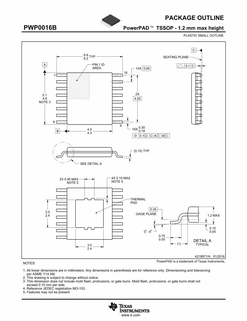
PACKAGE OUTLINE
C
TYP6.66.2
14X 0.65
16X 0.300.19
2X4.55
(0.15) TYP
0 - 80.150.05
3.02.4
3.02.4
2X 0.95 MAXNOTE 5
1.2 MAX
(1)
0.25GAGE PLANE
0.750.50
A
NOTE 3
5.14.9
B 4.54.3
4X 0.15 MAXNOTE 5
4218971/A 01/2016
PowerPAD TSSOP - 1.2 mm max heightPWP0016BPLASTIC SMALL OUTLINE
NOTES: 1. All linear dimensions are in millimeters. Any dimensions in parenthesis are for reference only. Dimensioning and tolerancing per ASME Y14.5M. 2. This drawing is subject to change without notice. 3. This dimension does not include mold flash, protrusions, or gate burrs. Mold flash, protrusions, or gate burrs shall not exceed 0.15 mm per side.4. Reference JEDEC registration MO-153.5. Features may not be present.
PowerPAD is a trademark of Texas Instruments.
TM
116
0.1 C A B
98
PIN 1 IDAREA
SEATING PLANE
0.1 C
SEE DETAIL A
DETAIL ATYPICAL
SCALE 2.400
THERMALPAD
www.ti.com
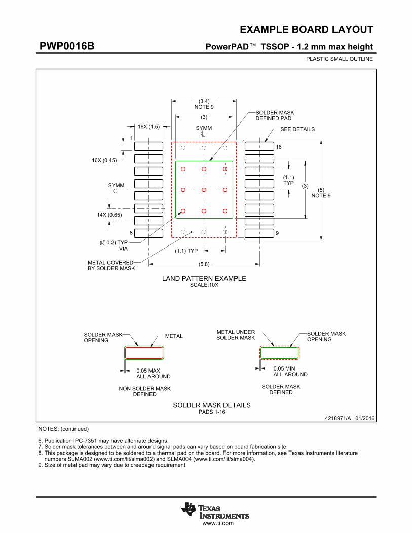
EXAMPLE BOARD LAYOUT
(5.8)
0.05 MAXALL AROUND
0.05 MINALL AROUND
16X (1.5)
16X (0.45)
14X (0.65)
(3.4)NOTE 9
(5)NOTE 9
(3)
(3)
( ) TYPVIA
0.2(1.1) TYP
(1.1)TYP
4218971/A 01/2016
PowerPAD TSSOP - 1.2 mm max heightPWP0016BPLASTIC SMALL OUTLINE
SYMM
SYMM
SEE DETAILS
LAND PATTERN EXAMPLESCALE:10X
1
8 9
16
METAL COVEREDBY SOLDER MASK
SOLDER MASKDEFINED PAD
TM
NOTES: (continued) 6. Publication IPC-7351 may have alternate designs. 7. Solder mask tolerances between and around signal pads can vary based on board fabrication site. 8. This package is designed to be soldered to a thermal pad on the board. For more information, see Texas Instruments literature numbers SLMA002 (www.ti.com/lit/slma002) and SLMA004 (www.ti.com/lit/slma004).9. Size of metal pad may vary due to creepage requirement.
METALSOLDER MASKOPENING
NON SOLDER MASKDEFINED
SOLDER MASK DETAILSPADS 1-16
SOLDER MASKDEFINED
SOLDER MASKMETAL UNDER SOLDER MASK
OPENING

www.ti.com
EXAMPLE STENCIL DESIGN
16X (1.5)
16X (0.45)
(3)
(3)BASED ON
0.125 THICKSTENCIL
14X (0.65)
(R ) TYP0.05
(5.8)
4218971/A 01/2016
PowerPAD TSSOP - 1.2 mm max heightPWP0016BPLASTIC SMALL OUTLINE
2.54 X 2.540.1752.74 X 2.740.15
3 X 3 (SHOWN)0.1253.35 X 3.350.1
SOLDER STENCILOPENING
STENCILTHICKNESS
NOTES: (continued) 10. Laser cutting apertures with trapezoidal walls and rounded corners may offer better paste release. IPC-7525 may have alternate design recommendations. 11. Board assembly site may have different recommendations for stencil design.
TM
SYMM
SYMM
1
89
16
BASED ON0.125 THICK
STENCIL
BY SOLDER MASKMETAL COVERED
SEE TABLE FORDIFFERENT OPENINGSFOR OTHER STENCILTHICKNESSES
SOLDER PASTE EXAMPLEEXPOSED PAD
100% PRINTED SOLDER COVERAGE BY AREASCALE:10X

IMPORTANT NOTICE
Texas Instruments Incorporated (TI) reserves the right to make corrections, enhancements, improvements and other changes to itssemiconductor products and services per JESD46, latest issue, and to discontinue any product or service per JESD48, latest issue. Buyersshould obtain the latest relevant information before placing orders and should verify that such information is current and complete.TI’s published terms of sale for semiconductor products (http://www.ti.com/sc/docs/stdterms.htm) apply to the sale of packaged integratedcircuit products that TI has qualified and released to market. Additional terms may apply to the use or sale of other types of TI products andservices.Reproduction of significant portions of TI information in TI data sheets is permissible only if reproduction is without alteration and isaccompanied by all associated warranties, conditions, limitations, and notices. TI is not responsible or liable for such reproduceddocumentation. Information of third parties may be subject to additional restrictions. Resale of TI products or services with statementsdifferent from or beyond the parameters stated by TI for that product or service voids all express and any implied warranties for theassociated TI product or service and is an unfair and deceptive business practice. TI is not responsible or liable for any such statements.Buyers and others who are developing systems that incorporate TI products (collectively, “Designers”) understand and agree that Designersremain responsible for using their independent analysis, evaluation and judgment in designing their applications and that Designers havefull and exclusive responsibility to assure the safety of Designers' applications and compliance of their applications (and of all TI productsused in or for Designers’ applications) with all applicable regulations, laws and other applicable requirements. Designer represents that, withrespect to their applications, Designer has all the necessary expertise to create and implement safeguards that (1) anticipate dangerousconsequences of failures, (2) monitor failures and their consequences, and (3) lessen the likelihood of failures that might cause harm andtake appropriate actions. Designer agrees that prior to using or distributing any applications that include TI products, Designer willthoroughly test such applications and the functionality of such TI products as used in such applications.TI’s provision of technical, application or other design advice, quality characterization, reliability data or other services or information,including, but not limited to, reference designs and materials relating to evaluation modules, (collectively, “TI Resources”) are intended toassist designers who are developing applications that incorporate TI products; by downloading, accessing or using TI Resources in anyway, Designer (individually or, if Designer is acting on behalf of a company, Designer’s company) agrees to use any particular TI Resourcesolely for this purpose and subject to the terms of this Notice.TI’s provision of TI Resources does not expand or otherwise alter TI’s applicable published warranties or warranty disclaimers for TIproducts, and no additional obligations or liabilities arise from TI providing such TI Resources. TI reserves the right to make corrections,enhancements, improvements and other changes to its TI Resources. TI has not conducted any testing other than that specificallydescribed in the published documentation for a particular TI Resource.Designer is authorized to use, copy and modify any individual TI Resource only in connection with the development of applications thatinclude the TI product(s) identified in such TI Resource. NO OTHER LICENSE, EXPRESS OR IMPLIED, BY ESTOPPEL OR OTHERWISETO ANY OTHER TI INTELLECTUAL PROPERTY RIGHT, AND NO LICENSE TO ANY TECHNOLOGY OR INTELLECTUAL PROPERTYRIGHT OF TI OR ANY THIRD PARTY IS GRANTED HEREIN, including but not limited to any patent right, copyright, mask work right, orother intellectual property right relating to any combination, machine, or process in which TI products or services are used. Informationregarding or referencing third-party products or services does not constitute a license to use such products or services, or a warranty orendorsement thereof. Use of TI Resources may require a license from a third party under the patents or other intellectual property of thethird party, or a license from TI under the patents or other intellectual property of TI.TI RESOURCES ARE PROVIDED “AS IS” AND WITH ALL FAULTS. TI DISCLAIMS ALL OTHER WARRANTIES ORREPRESENTATIONS, EXPRESS OR IMPLIED, REGARDING RESOURCES OR USE THEREOF, INCLUDING BUT NOT LIMITED TOACCURACY OR COMPLETENESS, TITLE, ANY EPIDEMIC FAILURE WARRANTY AND ANY IMPLIED WARRANTIES OFMERCHANTABILITY, FITNESS FOR A PARTICULAR PURPOSE, AND NON-INFRINGEMENT OF ANY THIRD PARTY INTELLECTUALPROPERTY RIGHTS. TI SHALL NOT BE LIABLE FOR AND SHALL NOT DEFEND OR INDEMNIFY DESIGNER AGAINST ANY CLAIM,INCLUDING BUT NOT LIMITED TO ANY INFRINGEMENT CLAIM THAT RELATES TO OR IS BASED ON ANY COMBINATION OFPRODUCTS EVEN IF DESCRIBED IN TI RESOURCES OR OTHERWISE. IN NO EVENT SHALL TI BE LIABLE FOR ANY ACTUAL,DIRECT, SPECIAL, COLLATERAL, INDIRECT, PUNITIVE, INCIDENTAL, CONSEQUENTIAL OR EXEMPLARY DAMAGES INCONNECTION WITH OR ARISING OUT OF TI RESOURCES OR USE THEREOF, AND REGARDLESS OF WHETHER TI HAS BEENADVISED OF THE POSSIBILITY OF SUCH DAMAGES.Unless TI has explicitly designated an individual product as meeting the requirements of a particular industry standard (e.g., ISO/TS 16949and ISO 26262), TI is not responsible for any failure to meet such industry standard requirements.Where TI specifically promotes products as facilitating functional safety or as compliant with industry functional safety standards, suchproducts are intended to help enable customers to design and create their own applications that meet applicable functional safety standardsand requirements. Using products in an application does not by itself establish any safety features in the application. Designers mustensure compliance with safety-related requirements and standards applicable to their applications. Designer may not use any TI products inlife-critical medical equipment unless authorized officers of the parties have executed a special contract specifically governing such use.Life-critical medical equipment is medical equipment where failure of such equipment would cause serious bodily injury or death (e.g., lifesupport, pacemakers, defibrillators, heart pumps, neurostimulators, and implantables). Such equipment includes, without limitation, allmedical devices identified by the U.S. Food and Drug Administration as Class III devices and equivalent classifications outside the U.S.TI may expressly designate certain products as completing a particular qualification (e.g., Q100, Military Grade, or Enhanced Product).Designers agree that it has the necessary expertise to select the product with the appropriate qualification designation for their applicationsand that proper product selection is at Designers’ own risk. Designers are solely responsible for compliance with all legal and regulatoryrequirements in connection with such selection.Designer will fully indemnify TI and its representatives against any damages, costs, losses, and/or liabilities arising out of Designer’s non-compliance with the terms and provisions of this Notice.
Mailing Address: Texas Instruments, Post Office Box 655303, Dallas, Texas 75265Copyright © 2017, Texas Instruments Incorporated