Embed Size (px)
Citation preview
Doping against the Native Propensity of MoS2: Degenerate HoleDoping by Cation SubstitutionJoonki Suh,† Tae-Eon Park,‡ Der-Yuh Lin,§ Deyi Fu,† Joonsuk Park,∥ Hee Joon Jung,⊥ Yabin Chen,†
Changhyun Ko,† Chaun Jang,‡ Yinghui Sun,¶ Robert Sinclair,∥ Joonyeon Chang,‡ Sefaattin Tongay,†,∇
and Junqiao Wu*,†,¶
†Department of Materials Science and Engineering, University of California, Berkeley, California 94720, United States‡Spin Convergence Research Center, Korea Institute of Science and Technology, Seoul 136-791, Korea§Department of Electronics Engineering, National Changhua University of Education, Changhua 50007, Taiwan∥Department of Materials Sciences and Engineering, Stanford University, Stanford, California 94305, United States⊥Energy and Environmental Directorate, Pacific Northwest National Laboratory, Richland, Washington 99352, United States¶Materials Sciences Division, Lawrence Berkeley National Laboratory, Berkeley, California 94720, United States
*S Supporting Information
ABSTRACT: Layered transition metal dichalcogenides (TMDs)draw much attention as the key semiconducting material for two-dimensional electrical, optoelectronic, and spintronic devices. Formost of these applications, both n- and p-type materials are neededto form junctions and support bipolar carrier conduction.However, typically only one type of doping is stable for aparticular TMD. For example, molybdenum disulfide (MoS2) isnatively an n-type presumably due to omnipresent electron-donating sulfur vacancies, and stable/controllable p-type dopinghas not been achieved. The lack of p-type doping hampers the development of charge-splitting p−n junctions of MoS2, as well aslimits carrier conduction to spin-degenerate conduction bands instead of the more interesting, spin-polarized valence bands.Traditionally, extrinsic p-type doping in TMDs has been approached with surface adsorption or intercalation of electron-accepting molecules. However, practically stable doping requires substitution of host atoms with dopants where the doping issecured by covalent bonding. In this work, we demonstrate stable p-type conduction in MoS2 by substitutional niobium (Nb)doping, leading to a degenerate hole density of ∼3 × 1019 cm−3. Structural and X-ray techniques reveal that the Nb atoms areindeed substitutionally incorporated into MoS2 by replacing the Mo cations in the host lattice. van der Waals p−n homojunctionsbased on vertically stacked MoS2 layers are fabricated, which enable gate-tunable current rectification. A wide range ofmicroelectronic, optoelectronic, and spintronic devices can be envisioned from the demonstrated substitutional bipolar doping ofMoS2. From the miscibility of dopants with the host, it is also expected that the synthesis technique demonstrated here can begenerally extended to other TMDs for doping against their native unipolar propensity.
KEYWORDS: transition-metal dichalcogenides, molybdenum disulfide, substitutional doping, p-type MoS2, p−n junction
In layered transition metal dichalcogenides (TMDs), eachlayer is weakly bonded to its neighbors by van der Waals
forces, thereby allowing physical or chemical isolation intoatomically thin semiconducting layers, as well as assembly ofjunctions free of lattice mismatch issues. A wide variety ofTMDs have been used as the active material to fabricateatomically thin field-effect transistors (FETs),1,2 integratedcircuits,3,4 and optoelectronic devices5−7 such as light-emittingdiodes, solar cells, and photodiodes.Similar to traditional semiconductor technologies, stable n-
and p-type conduction in the TMDs is indispensable for allthese applications. Yet in contrast, a bipolar doping strategy ofthe TMDs is currently lacking. Wisdom can be learned fromstudies of conventional semiconductors, where a native,unipolar doping propensity is usually found. For example, in
semiconductors such as CdO and InAs whose conduction bandminimum (CBM) and valence band maximum (VBM) lie lowwith respect to the vacuum level, native n-type conduction anddifficulty in p-type doping are observed; the opposite is true forsemiconductors such as Ge and diamond whose CBM andVBM lie high. This is attributed to the amphoteric dopingbehavior of electrically active native point defects,8 such asvacancies, interstitials, and defect complexes, which naturallyoccur in the materials in thermodynamic equilibrium.Extending this understanding to TMDs,9 it would be naturalto predict a native n-type (p-type) behavior of not intentionally
Received: August 24, 2014Revised: November 18, 2014Published: November 24, 2014
Letter
pubs.acs.org/NanoLett
© 2014 American Chemical Society 6976 dx.doi.org/10.1021/nl503251h | Nano Lett. 2014, 14, 6976−6982
doped MoS2 (WSe2), given the low (high)-lying CBM andVBM in MoS2 (WSe2) as seen in Figure 1a.Currently, modulation of carrier type and density in these
layered TMDs is achieved by means of electrostatic FETgating,7,10 metal work-function engineering,11,12 surface func-tionalization,13,14 or charge transfer from physic-sorbed volatilemolecules.15 However, to dope TMDs against their naturaldoping propensity, such as p-type in MoS2 (n-type in WS2)with very low VBM (high CBM), it is challenging to findmolecules capable of donating holes (electrons) effectively tothese low (high) - lying band edges. Moreover, practicalapplications require substitution of host atoms with dopants aspracticed in traditional semiconductors, where the doping issecured and stabilized by covalent bonding inside the lattice.Heterojunctions integrating different materials, such as n-typeMoS2 with p-type WSe2,
16,17 have been fabricated as analternative to homojunctions, but these heterostructures usuallysuffer from their type-II band offset. For example, it leads tolower photovoltages because the band offset curtails themaximum splitting of Fermi levels, as well as red-shifted lightemission due to recombination across the spatially indirectband edges.18,19
Indeed, for MoS2, consistent with the prediction above,recent electrical1−4,16,17 and optical20 investigations confirm itsnative n-doping, owing hypothetically to sulfur vacancies.21,22
The lack of p-type doping strictly limits carrier conduction inMoS2 to its conduction bands, despite the suggestion that p-type operation is more desirable for MoS2-based FET devices,10
and much more interest lies in its spin-polarized valence bandsfor the recently developed valleytronics.23,24 Niobium (Nb),which has one less valence electron than Mo, is theoreticallysuggested as the most suitable substitutional acceptor by
density-functional energetics/formation energies calculations.25
Moreover, MoS2 and NbS2 share the identical 2H crystalstructure, with similar lattice parameters, a = 3.16 and 3.32 Åand c = 12.29 and 11.94 Å for MoS2 and NbS2, respectively.
26
The covalent radius (Mo = 130 pm and Nb = 134 pm)27 andoxidation states of Mo and Nb in the 2H-polytype lattice arenearly identical. Indeed, fullerene-like MoxNb1−xS2 nano-particles28 and polycrystalline thin-films29 have been reported,but unambiguous p-type conduction and direct evidence of thesubstitutionality of doping have not been demonstrated insingle-crystal MoS2. In this work, we report stable p-typeconduction in MoS2 single crystals and ultrathin layers viasubstitutional Nb doping. The substitutionality of the Nbdopants in the MoS2 crystals is confirmed by structural andchemical analysis techniques, and the degenerate p-typeconduction is evaluated by Hall-effect and gated transportstudies. Prototypical p−n homojunctions built from verticallystacked MoS2 layers show current rectification tunable by a gatevoltage.
Results and Discussions. The Nb-doped MoS2(MoS2:Nb) single crystals were grown by a chemical vaportransport (CVT) method using iodine as the transport agent,an approach that has been employed to prepare other layeredcompounds with high quality.30,31 A horizontal three-zonefurnace was utilized where the high (low) temperature zonewas used as the reaction (growth) zone, as seen in SupportingInformation Figure S1. Prior to the crystal growth, a quartztube containing the transport agent and the elements requiredfor the doped crystals was evacuated to below 10−6 Torr andsecurely sealed. The purity of the source materials was Mo99.99%, S 99.99%, and Nb 99.99%, with a molar ratio ofMo:S:Nb equal to 1:2:0.005 for a nominal 0.5% Nb doping.
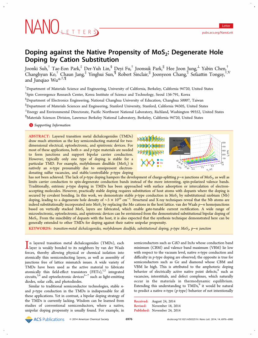
Figure 1. Structural and chemical analyses of Nb-doped MoS2 (MoS2:Nb). (a) Band-edge (CBM and VBM) alignment of representativeconventional semiconductors and TMDs, referenced to the vacuum level. (b) Cross-section illustration of van der Waals coupled MoS2:Nb layerswhere Nb dopants replace the Mo host atoms in a substitutional manner. A digital photograph inset shows a synthesized MoS2:Nb crystal with ascale bar of 3 mm. (c) HRTEM image of the MoS2:Nb with the corresponding FFT in the inset. (d) Cs (spherical aberration)-corrected HRTEMimage with subangstrom resolution acquired from the monolayer part. (e) Transmitted electron intensity along the vertical direction ofcorresponding blue box denoted in panel d. (f) EFTEM-SI maps of elastic (0 eV), Mo M4,5, Nb M2, and S L2,3 measured from the same region of theMoS2:Nb sample. Scale bars are 100 nm. (g) XPS scans of the Nb 3d (top), the Mo 3d, and S 2s (both in bottom) core-levels measured from theNb-doped and undoped MoS2.
Nano Letters Letter
dx.doi.org/10.1021/nl503251h | Nano Lett. 2014, 14, 6976−69826977
The sealed quartz tube was then inserted into the three-zonefurnace. In the beginning, the temperature of the growth zonewas set to 1000 °C for 12 h to remove any possible residues.The process of the CVT was initiated with a temperaturegradient varying from 1050 °C in the reaction zone to 935 °Cin the growth zone over a distance of ∼30 cm, and the systemwas held in this condition over 500 h in order to providesufficient diffusion and equilibration for the single-crystalsynthesis. The CVT growth yielded large, thin, and shinyMoS2:Nb crystals that are typically a few millimeters in lateralsize with high crystallinity (Figure 1b). Similar to other TMDs,these as-synthesized MoS2:Nb crystals are exfoliation-ready,and the number of exfoliated layers can be determined byRaman spectroscopy and atomic force microscopy (SupportingInformation Figure S2).To determine the crystal structure and evaluate the
crystallinity of the MoS2:Nb, we deployed extensive high-resolution transmission electron microscopy (HRTEM)measurements over a wide area on multiple samples. The as-synthesized MoS2:Nb is single crystalline, exhibiting ahexagonal lattice as seen from the fast-Fourier transform(FFT) pattern displayed in the inset of Figure 1c (see alsoselected area electron diffraction pattern in SupportingInformation Figure S3a). The estimated lattice spacing of 1.6and 2.7 Å, corresponding to the (110) and (100) planes,respectively, is consistent with reported values.32 Cross-sectional HRTEM images also show highly parallel layerstacking with an interlayer separation of approximately 6.15 Å(Supporting Information Figure S3b). The Cs (sphericalaberration)-corrected atomic HRTEM image in Figure 1dclearly reveals hexagonal rings formed by the S atoms (dimmersites) together with the transition metal atoms, the Mo atomsor Nb dopants (brighter sites) supported by the correspondingintensity profiles presented in Figure 1e. It is noted thatstructural imperfections such as grain boundaries, dislocations,and atomic defects were not observed from the HRTEM.Energy-filtered electron transmission microscopy spectrumimaging (EFTEM-SI) was subsequently used to probe thechemical composition of the MoS2:Nb with nanoscale spatialresolution, in particular, the incorporation of Nb dopants intothe lattice. As seen in Figure 1f, the Nb signal was well resolvedthrough its M2 peak (∼378 eV) and is indeed uniformlydispersed in the MoS2 matrix with no evidence of clustering(also see the corresponding electron energy loss spectrum inSupporting Information Figure S3c).The Nb dopants in the MoS2 crystals were further analyzed
with X-ray photoelectron spectroscopy (XPS). Distinct bindingenergy peaks associated with the Nb 3d core levels at 203.6 and206.1 eV were detected only in the MoS2:Nb samples (Figure1g), and they well match previously observed XPS featuresfrom fullerene-like Mo1−xNbxS2 nanoparticles.28 In addition,the core-level peaks of Mo and S in the MoS2:Nb show auniform shift toward lower binding energies compared to thoseof the undoped MoS2. This shift is attributed to lowering of theFermi level (EF) upon the p-type doping, as similarly observedin previous studies.28,33 The amount of EF downshift, ∼ 0.7 eV,is found to be consistent with the MoS2 band gap of 1.2 eV34
and the degenerate p-doping.Recent reports have suggested many possible, nonsubstitu-
tional atomic configurations for dopants in MoS2, for example,adatom35 or intercalation.36 Therefore, it is important toevaluate the substitutionality of Nb in the MoS2 lattice. BecauseNb and Mo atoms are adjacent to each other on the periodic
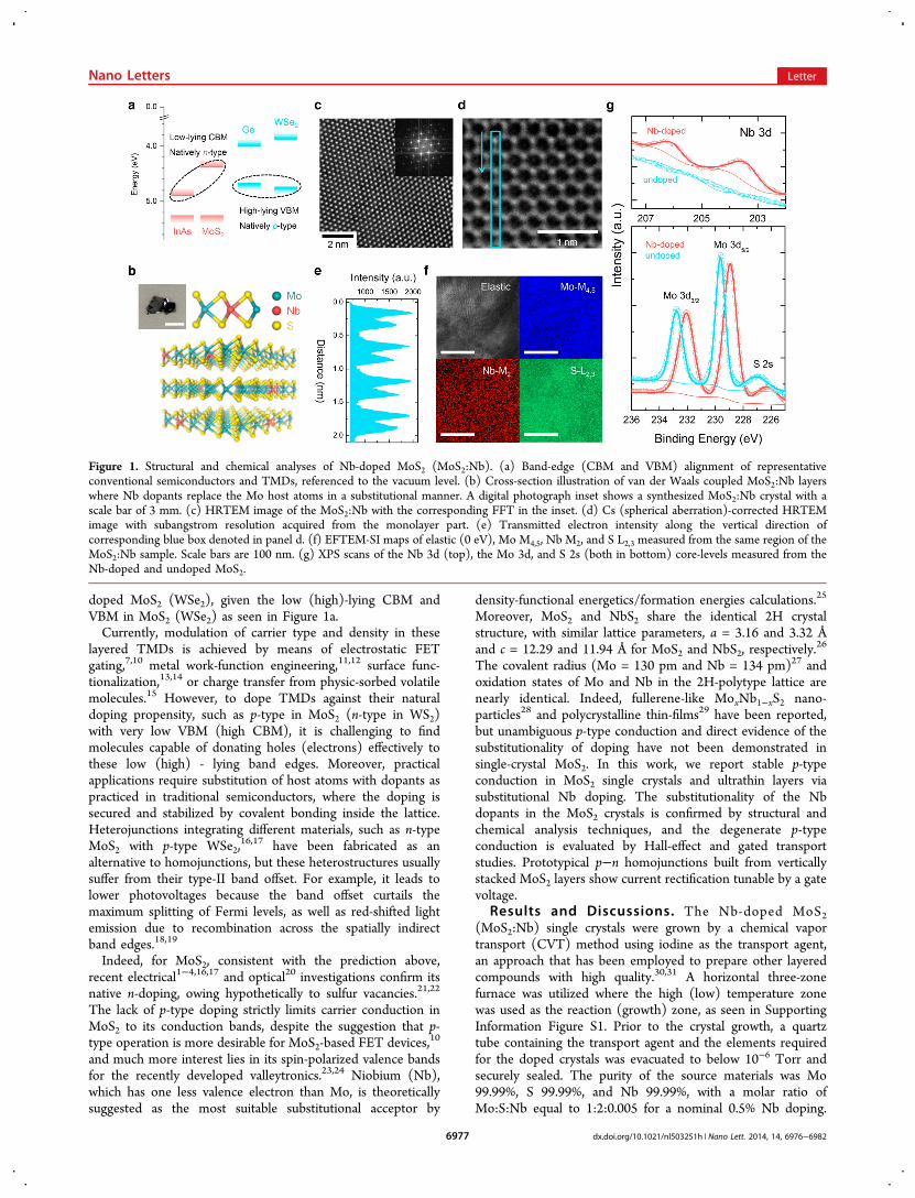
table, it is rather difficult to distinguish them in the HRTEM,and more chemically sensitive characterization techniques arerequired to determine the location of Nb dopants. Extended X-ray absorption fine structure (EXAFS) analysis is ideally suitedfor this purpose, allowing for determination of local environ-ment around the X-ray absorbing atoms. By analyzingoscillations in the normalized X-ray absorption data,37,38 criticalinformation can be extracted, such as local coordinationnumber (N), interatomic distance to neighboring atoms (r),and the Debye−Waller disorder parameter (σ2). Despite theiradjacent atomic numbers, the K edge energies of Nb and Moare widely separated by ∼1 keV (Nb = 18.99 keV and Mo =20.01 keV), and this provides sufficient energy span to fullyresolve their EXAFS oscillations in the postabsorption spectralregion. Figure 2a shows the normalized absorption data for the
Nb and Mo K edges, collected in the fluorescence andtransmission mode, respectively. Figure 2b shows the extractedEXAFS oscillations, k3-weighted χ(k), along with the result ofbest fitting to the data. The fitting was determined by Fouriertransforming the χ(k) across a k-range up to 15 Å−1 consideringthe first two coordination shells for both the Nb and Mo Kedges (see detailed fitting parameters in the SupportingInformation).The results show nearly identical N and r, and thus local
atomic bonding environment for the Nb and Mo atoms, clearlyindicating the substitutional nature of Nb atoms. The Fouriertransformed k3-weighted EXAFS is plotted in Figure 2cshowing two distinct peaks at two radial distances. The first
Figure 2. EXAFS analysis on Nb-doped MoS2: Evidence forsubstitutional doping. (a) Raw X-ray absorption data for the Nb andMo K edges normalized by peak intensity. (b) EXAFS oscillationsextracted from the absorption data weighted by k3. (c) Radialdistribution of Fourier-transformed EXAFS signal. Points are rawexperimental data while red and green lines are best fits for the Nb andMo K edge, respectively.
Nano Letters Letter
dx.doi.org/10.1021/nl503251h | Nano Lett. 2014, 14, 6976−69826978
peak corresponds to atomic bonds with S atoms, the nearestneighbor of the transition metal atoms, and the second peak isassociated with intralayer cation (transition metal) neighbors.These bond lengths agree quantitatively with those measured inMoS2 single crystals.39 Here, though scattering from the firstand second nearest neighbors of the X-ray absorbing cationatoms is evident, the existence of the interlayer van der Waalsgap may damp contributions from neighbors at greaterdistances. We also note that σ2 is quite narrow, despite thatthe data was collected in ambient air at 300 K, which furtherconfirms the high crystal quality in agreement with theHRTEM measurements.We measured the p-type electrical conduction in a thin flake
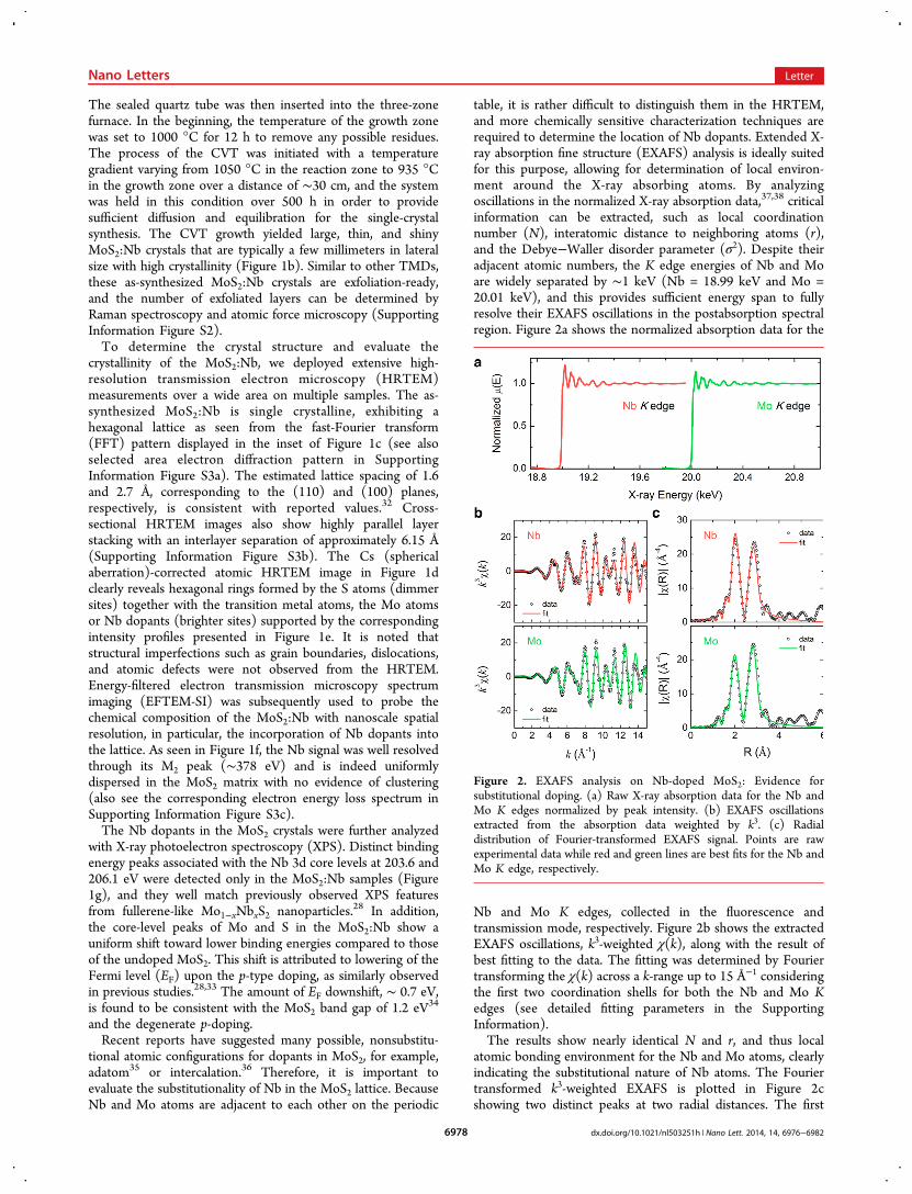
mechanically exfoliated from the MoS2:Nb crystals usingvariable-temperature Hall effect. The multilayer MoS2:NbHall device was fabricated on a 300 nm SiO2/Si substrate,and standard e-beam lithography (EBL) was used to define theflake into a Hall bar configuration as seen in Figure 3a. Afteretching the unwanted area with XeF2 gas, a second EBL wasperformed to pattern the voltage leads and current injectionelectrodes, followed by deposition of Ti/Au (5/100 nm) metalcontacts (see experimental details in the Supporting Informa-tion). As shown in Supporting Information Figure S4, two-probe I−V curves displayed linear characteristics, suggestingohmic contacts, despite the Schottky barrier expected betweenthe MoS2 valence band and Ti (surface potential-energy barrierΦB ∼ 1.0 eV, estimated from the Ti work function 4.33 eV andthe VBM of MoS2 (ref 9)). This is attributed to the degeneratep-type doping resulting in very narrow depletion width of a fewnanometers, thereby allowing significant tunneling current toflow as typically occurring in heavily doped semiconduc-tors.40,41
The measured Hall resistance, Rxy, is plotted as a function ofthe magnetic field (B) in Figure 3b. The magnetic field wasvaried up to 4 T, and both current injection directions wereused in order to remove influence of possible misalignment ofvoltage electrodes from the longitudinal resistance Rxx; that is,the treatment is equivalent to Rxy(B) = (Vxy(+B) − Vxy(−B))/2Ixx.
42 The results confirm the p-type conduction of MoS2:Nb,as well as reveal a constancy of the Hall coefficient RH(= Rxy/B= −1/p2De) over a wide range of temperature. Linear fitting inFigure 3b yields a high sheet hole concentration (p2D) of 1.8 ×1014 cm−2, corresponding to a bulk concentration of 3.0 × 10¹⁹
cm−3, far exceeding the critical hole concentration fordegenerate p-type doping in MoS2 (see Supporting Informa-tion). The absence of carrier freeze-out (Figure 3c) indicates adegenerate level of doping, and such a dense hole concentrationin the degenerate limit is indeed in good agreement with thenominal doping concentration of Nb as analyzed below,suggesting the tunability of the doping level with varying thedopant concentration. Using the assumption that each of theNb atoms acts as a single acceptor,27 p2D
nominal is estimated fromthe 0.5% Nb doping to be ∼2.8 × 1014 cm−2, showing goodconsistency with the measured p2D considering the unknowndegree of charge compensation by the donor-like sulfurvacancies. We also note that a nearly identical hole density isobserved from another Hall device. Combined with the four-terminal Rxx data presented in Figure 3d and geometricalfactors of the Hall device, the Hall mobility (μ) was extracted,which shows a monotonic increase with temperature. This is afurther signature of degenerately doped semiconductors,43
where ionized impurity scattering dominates over phononscattering even at room temperature. This is the opposite to thebehavior of intrinsic MoS2 crystals, where acoustic phonon
Figure 3. Hall-effect measurement of MoS2:Nb microdevices. (a) Optical microscopy image of a Hall-bar device based on a multilayer (61 nm thick,determined by atomic force microscopy) MoS2:Nb flake (Scale bar =10 μm). (b) Hall resistance, Rxy, as a function of magnetic field at threerepresentative temperatures (10, 200, and 300 K). Blank circles and colored lines are the measured data and linear fits, respectively. (c) Calculatedhole sheet concentration (red) and Hall-effect mobility (blue) as a function of temperature from 10 to 300 K. (d) Longitudinal resistance Rxx of theHall-bar device as a function of temperature.
Nano Letters Letter
dx.doi.org/10.1021/nl503251h | Nano Lett. 2014, 14, 6976−69826979
scattering plays a much greater role in limiting μ at roomtemperature.2
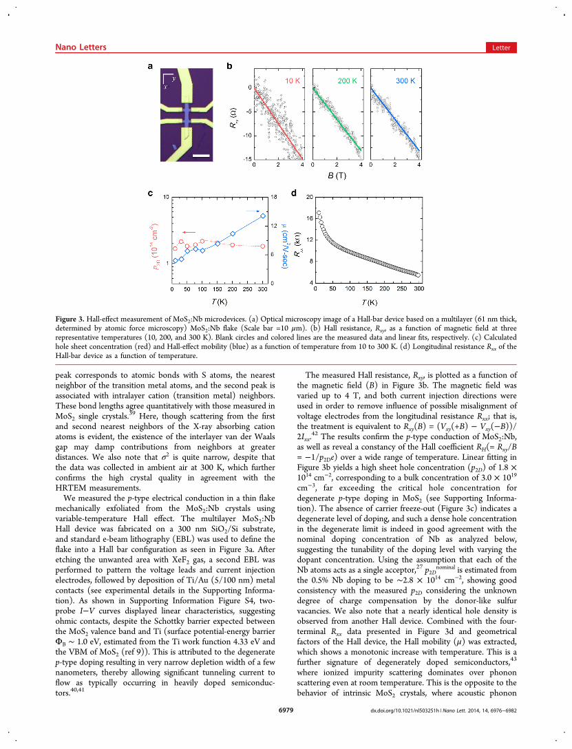
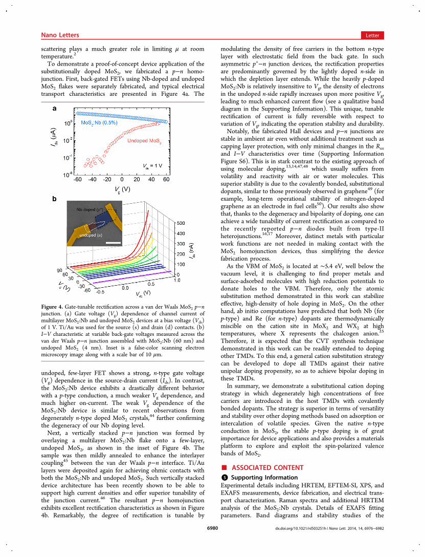
To demonstrate a proof-of-concept device application of thesubstitutionally doped MoS2, we fabricated a p−n homo-junction. First, back-gated FETs using Nb-doped and undopedMoS2 flakes were separately fabricated, and typical electricaltransport characteristics are presented in Figure 4a. The
undoped, few-layer FET shows a strong, n-type gate voltage(Vg) dependence in the source-drain current (Ids). In contrast,the MoS2:Nb device exhibits a drastically different behaviorwith a p-type conduction, a much weaker Vg dependence, andmuch higher on-current. The weak Vg dependence of theMoS2:Nb device is similar to recent observations fromdegenerately n-type doped MoS2 crystals,
44 further confirmingthe degeneracy of our Nb doping level.Next, a vertically stacked p−n junction was formed by
overlaying a multilayer MoS2:Nb flake onto a few-layer,undoped MoS2, as shown in the inset of Figure 4b. Thesample was then mildly annealed to enhance the interlayercoupling45 between the van der Waals p−n interface. Ti/Aulayers were deposited again for achieving ohmic contacts withboth the MoS2:Nb and undoped MoS2. Such vertically stackeddevice architecture has been recently shown to be able tosupport high current densities and offer superior tunability ofthe junction current.46 The resultant p−n homojunctionexhibits excellent rectification characteristics as shown in Figure4b. Remarkably, the degree of rectification is tunable by
modulating the density of free carriers in the bottom n-typelayer with electrostatic field from the back gate. In suchasymmetric p+−n junction devices, the rectification propertiesare predominantly governed by the lightly doped n-side inwhich the depletion layer extends. While the heavily p-dopedMoS2:Nb is relatively insensitive to Vg, the density of electronsin the undoped n-side rapidly increases upon more positive Vg,leading to much enhanced current flow (see a qualitative banddiagram in the Supporting Information). This unique, tunablerectification of current is fully reversible with respect tovariation of Vg, indicating the operation stability and durability.Notably, the fabricated Hall devices and p−n junctions are
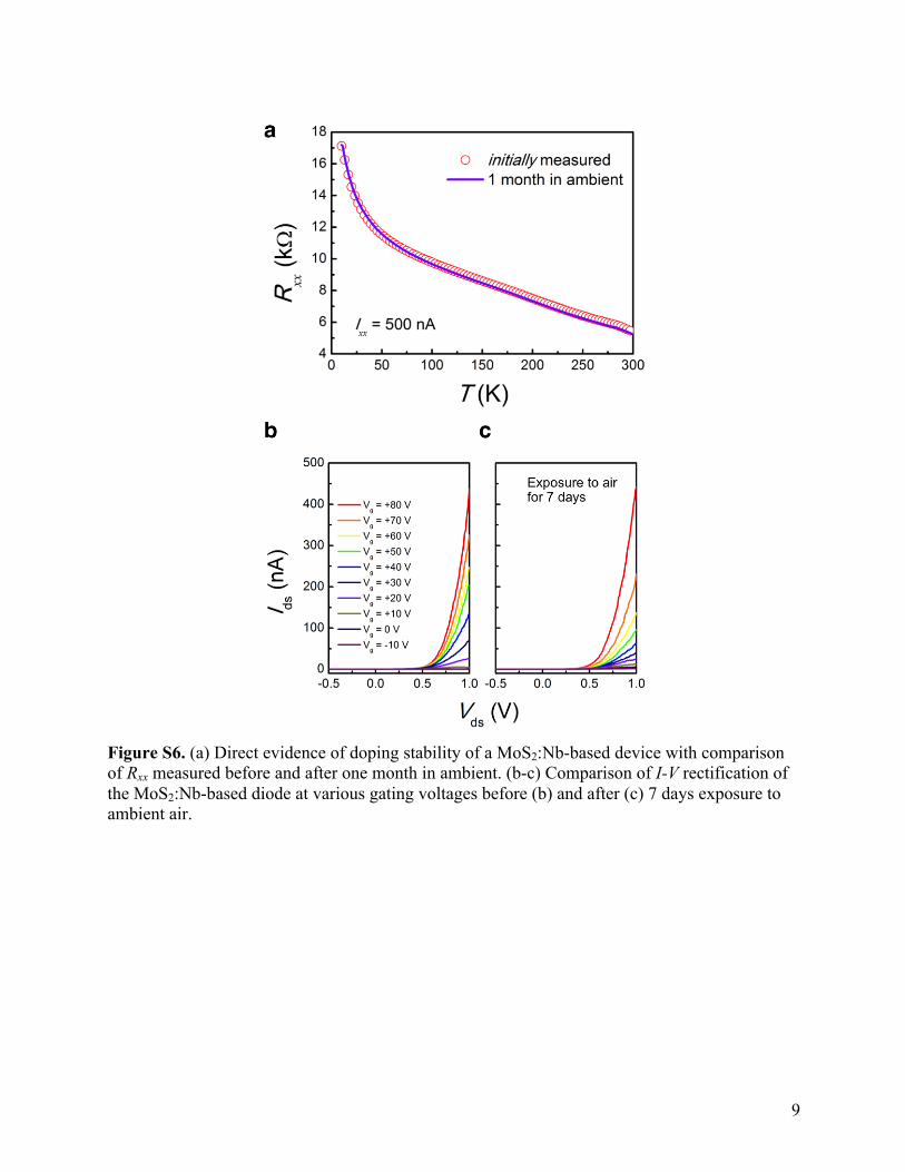
stable in ambient air even without additional treatment such ascapping layer protection, with only minimal changes in the Rxxand I−V characteristics over time (Supporting InformationFigure S6). This is in stark contrast to the existing approach ofusing molecular doping,13,14,47,48 which usually suffers fromvolatility and reactivity with air or water molecules. Thissuperior stability is due to the covalently bonded, substitutionaldopants, similar to those previously observed in graphene49 (forexample, long-term operational stability of nitrogen-dopedgraphene as an electrode in fuel cells50). Our results also showthat, thanks to the degeneracy and bipolarity of doping, one canachieve a wide tunability of current rectification as compared tothe recently reported p−n diodes built from type-IIheterojunctions.16,17 Moreover, distinct metals with particularwork functions are not needed in making contact with theMoS2 homojunction devices, thus simplifying the devicefabrication process.As the VBM of MoS2 is located at ∼5.4 eV, well below the
vacuum level, it is challenging to find proper metals andsurface-adsorbed molecules with high reduction potentials todonate holes to the VBM. Therefore, only the atomicsubstitution method demonstrated in this work can stabilizeeffective, high-density of hole doping in MoS2. On the otherhand, ab initio computations have predicted that both Nb (forp-type) and Re (for n-type) dopants are thermodynamicallymiscible on the cation site in MoX2 and WX2 at hightemperatures, where X represents the chalcogen anion.25
Therefore, it is expected that the CVT synthesis techniquedemonstrated in this work can be readily extended to dopingother TMDs. To this end, a general cation substitution strategycan be developed to dope all TMDs against their nativeunipolar doping propensity, so as to achieve bipolar doping inthese TMDs.In summary, we demonstrate a substitutional cation doping
strategy in which degenerately high concentrations of freecarriers are introduced in the host TMDs with covalentlybonded dopants. The strategy is superior in terms of versatilityand stability over other doping methods based on adsorption orintercalation of volatile species. Given the native n-typeconduction in MoS2, the stable p-type doping is of greatimportance for device applications and also provides a materialsplatform to explore and exploit the spin-polarized valencebands of MoS2.
■ ASSOCIATED CONTENT*S Supporting InformationExperimental details including HRTEM, EFTEM-SI, XPS, andEXAFS measurements, device fabrication, and electrical trans-port characterization. Raman spectra and additional HRTEManalysis of the MoS2:Nb crystals. Details of EXAFS fittingparameters. Band diagrams and stability studies of the
Figure 4. Gate-tunable rectification across a van der Waals MoS2 p−njunction. (a) Gate voltage (Vg) dependence of channel current ofmultilayer MoS2:Nb and undoped MoS2 devices at a bias voltage (Vds)of 1 V. Ti/Au was used for the source (s) and drain (d) contacts. (b)I−V characteristic at variable back-gate voltages measured across thevan der Waals p−n junction assembled with MoS2:Nb (60 nm) andundoped MoS2 (4 nm). Inset is a false-color scanning electronmicroscopy image along with a scale bar of 10 μm.
Nano Letters Letter
dx.doi.org/10.1021/nl503251h | Nano Lett. 2014, 14, 6976−69826980
fabricated devices. This material is available free of charge viathe Internet at http://pubs.acs.org.
■ AUTHOR INFORMATIONCorresponding Author* E-mail: [email protected] Address∇School for Engineering of Matter, Transport and Energy,Arizona State University, Tempe, Arizona 85287, United States.Author ContributionsThe manuscript was written through contributions of allauthors. All authors have given approval to the final version ofthe manuscript.NotesThe authors declare no competing financial interest.
■ ACKNOWLEDGMENTSThis work was supported by the National Science Foundationunder Grant No. DMR-1306601. J.W. and Y.C. acknowledgesupport from the Singapore-Berkeley Research Initiative forSustainable Energy (SinBeRISE). T.-E.P., C.J., and J.C. weresupported by KIST Institutional program. D.-Y.L. acknowl-edges support by the National Science Council of Taiwanunder Grant No. NSC 102-2112-M-018-002. Use of theStanford Synchrotron Radiation Light source (SLAC NationalAccelerator Laboratory) and XPS at the Molecular Foundry issupported by the U.S. Department of Energy, Office of Science,Office of Basic Energy Sciences under Contract No. DE-AC02-76SF00515 and DE-AC02-05CH11231, respectively. We thankDr. D. Frank Ogletree, Erik J. Nelson, and Junko Yano forassistance with XPS and EXAFS measurements, Dr. YeonbaeLee for the transport measurements, and Prof. Mike Crommiefor use of the alignment microscope. Use of the FEI Titan 80-300 ETEM at Stanford Nanocharacterization Lab and JEOLARM 200cF at the Pacific Northwest National Lab are alsoacknowledged.
■ REFERENCES(1) Radisavljevic, B.; Radenovic, A.; Brivio, J.; Giacometti, V.; Kis, A.Nat. Nanotechnol. 2011, 6, 147−150.(2) Kim, S.; Konar, A.; Hwang, W.-S.; Lee, J. H.; Lee, J.; Yang, J.;Jung, C.; Kim, H.; Yoo, J.-B.; Choi, J.-Y.; Jin, Y. W.; Lee, S. Y.; Jena, D.;Choi, W.; Kim, K. Nat. Commun. 2012, 3, 1011.(3) Radisavljevic, B.; Whitwick, M. B.; Kis, A. ACS Nano 2011, 5,9934−9938.(4) Wang, H.; Yu, L.; Lee, Y.-H.; Shi, Y.; Hsu, A.; Chin, M. L.; Li, L.-J.; Dubey, M.; Kong, J.; Palacios, T. Nano Lett. 2012, 12, 4674−4680.(5) Pospischil, A.; Furchi, M. M.; Mueller, T. Nat. Nanotechnol. 2014,9, 257−261.(6) Baugher, B. W. H.; Churchill, H. O. H.; Yang, Y.; Jarillo-Herrero,P. Nat. Nanotechnol. 2014, 9, 262−267.(7) Ross, J. S.; Klement, P.; Jones, A. M.; Ghimire, N. J.; Yan, J.;Mandrus, D. G.; Taniguchi, T.; Watanabe, K.; Kitamura, K.; Yao, Y.;Cobden, D. H.; Xu, X. Nat. Nanotechnol. 2014, 9, 268−272.(8) Walukiewicz, W. Physica B 2001, 302−303, 123−134.(9) Kang, J.; Tongay, S.; Zhou, J.; Li, J.; Wu, J. Appl. Phys. Lett. 2013,102, 012111.(10) Zhang, Y. J.; Ye, J. T.; Yomogida, Y.; Takenobu, T.; Iwasa, Y.Nano Lett. 2013, 13, 3023−3028.(11) Chuang, S.; Battaglia, C.; Azcatl, A.; McDonnell, S.; Kang, J. S.;Yin, X.; Tosun, M.; Kapadia, R.; Fang, H.; Wallace, R. M.; Javey, A.Nano Lett. 2014, 14, 1337−1342.(12) Fontana, M.; Deppe, T.; Boyd, A. K.; Rinzan, M.; Liu, A. Y.;Paranjape, M.; Barbara, P. Sci. Rep. 2013, 3, 1634.
(13) Mouri, S.; Miyauchi, Y.; Matsuda, K. Nano Lett. 2013, 13,5944−5948.(14) Lin, J. D.; Han, C.; Wang, F.; Wang, R.; Xiang, D.; Qin, S.;Zhang, X.-A.; Wang, L.; Zhang, H.; Wee, A. T. S.; Chen, W. ACS Nano2014, 8, 5323−5329.(15) Tongay, S.; Zhou, J.; Ataca, C.; Liu, J.; Kang, J. S.; Matthews, T.S.; You, L.; Li, J.; Grossman, J. C.; Wu, J. Nano Lett. 2013, 13, 2831−2836.(16) Lee, C.-H.; Lee, G.-H.; Van der Zande, A. M.; Chen, W.; Li, Y.;Han, M.; Cui, X.; Arefe, G.; Nuckolls, C.; Heinz, T. F.; Guo, J.; Hone,J.; Kim, P. Nat. Nanotech. 2014, advanced online publication (DOI:10.1038/nnano.2014.150).(17) Fang, H.; Battaglia, C.; Carraro, C.; Nemsak, S.; Ozdol, B.;Kang, J. S.; Bechtel, H. A.; Desai, S. B.; Kronast, F.; Unal, A. A.; Conti,G.; Conlon, C.; Palsson, G. K.; Martin, M. C.; Minor, A. M.; Fadley, C.S.; Yablonovitch, E.; Maboudian, R.; Javey, A. Proc. Natl. Acad. Sci.U.S.A. 2014, 111, 6198−6202.(18) Borys, N. J.; Walter, M. J.; Huang, J.; Talapin, D. V.; Lupton, J.M. Science 2010, 330, 1371−1374.(19) Seidel, W.; Titkov, A.; Andre,́ J. P.; Voisin, P.; Voos, M. Phys.Rev. Lett. 1994, 73, 2356−2359.(20) Mak, K. F.; He, K. L.; Lee, C.; Lee, G. H.; Hone, J.; Heinz, T. F.;Shan, J. Nat. Mater. 2013, 12, 207−211.(21) Qiu, H.; Xu, T.; Wang, Z.; Ren, W.; Nan, H.; Ni, Z.; Chen, Q.;Yuan, S.; Miao, F.; Song, F.; Long, G.; Shi, Y.; Sun, L.; Wang, J.; Wang,X. Nat. Commun. 2013, 4, 2642.(22) Tongay, S.; Suh, J.; Ataca, C.; Fan, W.; Luce, A.; Kang, J. S.; Liu,J.; Ko, C.; Raghunathanan, R.; Zhou, J.; Ogletree, F.; Li, J.; Grossman,J. C.; Wu, J. Sci. Rep. 2013, 3, 2657.(23) Mak, K. F.; He, K.; Shan, J.; Heinz, T. F. Nat. Nanotechnol.2012, 7, 494−498.(24) Suzuki, R.; Sakano, M.; Zhang, Y. J.; Akashi, R.; Morikawa, D.;Harasawa, A.; Yaji, K.; Kuroda, K.; Miyamoto, K.; Okuda, T.; Ishizaka,K.; Arita, R.; Iwasa, Y. Nat. Nanotechnol. 2014, 9, 611−617.(25) Dolui, K.; Rungger, I.; Pemmaraju, C. D.; Sanvito, S. Phys. Rev. B2013, 88, 075420.(26) Wilson, J. A.; Yoffe, A. D. Adv. Phys. 1969, 18, 193−335.(27) Ivanovskaya, V. V.; Zobelli, A.; Gloter, A.; Brun, N.; Serin, V.;Colliex, C. Phys. Rev. B 2008, 78, 134104.(28) Deepak, F. L.; Cohen, H.; Cohen, S.; Feldman, Y.; Popovitz-Biro, R.; Azulay, D.; Millo, O.; Tenne, R. J. Am. Chem. Soc. 2007, 129,12549−12562.(29) Laskar, M. R.; Nath, D. N.; Ma, L.; Lee, E. W., II; Lee, C. H.;Kent, T.; Yang, Z.; Mishra, R.; Roldan, M. A.; Idrobo, J.-C.; Pantelides,S. T.; Pennycook, S. J.; Myers, R. C.; Wu, Y.; Rajan, S. Appl. Phys. Lett.2014, 104, 092104.(30) Tongay, S.; Sahin, H.; Ko, C.; Luce, A.; Fan, W.; Liu, K.; Zhou,J.; Huang, Y.-S.; Ho, C.-H.; Yan, J.; Ogletree, D. F.; Aloni, S.; Ji, J.; Li,S.; Li, J.; Peeters, F. M.; Wu, J. Nat. Commun. 2014, 5, 3252.(31) Tongay, S.; Narang, D. S.; Kang, J.; Fan, W.; Ko, C.; Luce, A. V.;Wang, K. X.; Suh, J.; Patel, K. D.; Pathak, V. M.; Li, J.; Wu, J. Appl.Phys. Lett. 2014, 104, 012101.(32) Lee, Y.-H.; Zhang, X.-Q.; Zhang, W.; Chang, M.-T.; Lin, C.-T.;Chang, K.-D.; Yu, Y.-C.; Wang, J. T.-W.; Chang, C.-S.; Li, L.-J.; Lin, T.-W. Adv. Mater. 2012, 24, 2320−2325.(33) McDonnell, S.; Addou, R.; Buie, C.; Wallace, R. M.; Hinkle, C.L. ACS Nano 2014, 8, 2880−2888.(34) Kam, K. K.; Parkinson, B. A. J. Phys. Chem. 1982, 86, 463−467.(35) Lin, Y.-C.; Dumcenco, D. O.; Komsa, H.-P.; Niimi, Y.;Krasheninnikov, A. V.; Huang, Y.-S.; Suenaga, K. Adv. Mater. 2014,26, 2857−2861.(36) Remskar, M.; Skraba, Z.; Stadelmann, P.; Levy, F. Adv. Mater.2000, 12, 814−818.(37) Levander, A. X.; Yu, K. M.; Novikov, S. V.; Liliental-Weber, Z.;Foxon, C. T.; Dubon, O. D.; Wu, J.; Walukiewicz, W. J. Appl. Phys.2013, 113, 243505.(38) Metha, A.; Nelson, E. J.; Webb, S. M.; Holt, J. K. Adv. Mater.2009, 21, 102−106.
Nano Letters Letter
dx.doi.org/10.1021/nl503251h | Nano Lett. 2014, 14, 6976−69826981
(39) Joensen, P.; Crozier, E. D.; Alberding, N.; Frindt, R. F. J. Phys.C: Solid State Phys. 1987, 20, 4043−4053.(40) Baca, A. G.; Ren, F.; Zolper, J. C.; Briggs, R. D.; Pearton, S. J.Thin Solid Films 1997, 308−309, 599−606.(41) Park, T.-E.; Min, B.-C.; Kim, I.; Yang, J.-E.; Jo, M.-H.; Chang, J.;Choi, H.-J. Nano Lett. 2011, 11, 4730−4735.(42) Pradhan, N. R.; Rhodes, D.; Xin, Y.; Memaran, S.; Bhaskaran, L.;Siddiq, M.; Hill, S.; Ajayan, P. M.; Balicas, L. ACS Nano 2014,No. 10.1021/nn501693d.(43) Bauer, G.; Kahlert, H. Phys. Rev. B 1972, 5, 566−579.(44) Kiriya, D.; Tosun, M.; Zhao, P.; Kang, J. S.; Javey, A. J. Am.Chem. Soc. 2014, 136, 7853−7856.(45) Tongay, S.; Fan, W.; Kang, J.; Park, J.; Koldemir, U.; Suh, J.;Narang, D. S.; Liu, K.; Ji, J.; Li, J.; Sinclair, R.; Wu, J. Nano Lett. 2014,14, 3185−3190.(46) Yu, W. J.; Liu, Y.; Zhou, H.; Yin, A.; Li, Z.; Huang, Y.; Duan, X.Nat. Nanotechnol. 2013, 8, 952−958.(47) Fang, H.; Tosun, M.; Seol, G.; Chang, T. C.; Takei, K.; Guo, J.;Javey, A. Nano Lett. 2013, 13, 1991−1995.(48) Fang, H.; Chuang, S.; Chang, T. C.; Takei, K.; Takahashi, T.;Javey, A. Nano Lett. 2012, 12, 3788−3792.(49) Liu, H.; Liu, Y.; Zhu, D. J. Mater. Chem. 2011, 21, 3335−3345.(50) Qu, L.; Liu, Y.; Baek, J.-B.; Dai, L. ACS Nano 2010, 4, 1321−1326.
Nano Letters Letter
dx.doi.org/10.1021/nl503251h | Nano Lett. 2014, 14, 6976−69826982
1
Supporting Information for “Doping against the native propensity of MoS2: degenerate hole doping by cation substitution” Joonki Suh,1 Tae-Eon Park,2 Der-Yuh Lin,3 Deyi Fu,1 Joonsuk Park,4 Hee Joon Jung,5 Yabin Chen,1 Changhyun Ko,1 Chaun Jang,2 Yinghui Sun,6 Robert Sinclair,4 Joonyeon Chang,2 Sefaattin Tongay,1 Junqiao Wu1,6,*
1 Department of Materials Science and Engineering, University of California, Berkeley, California 94720, USA 2 Spin Convergence Research Center, Korea Institute of Science and Technology, Seoul 136-791, Korea 3 Department of Electronics Engineering, National Changhua University of Education, Changhua 50007, Taiwan 4 Department of Materials Sciences and Engineering, Stanford University, Stanford, California 94305, USA 5 Energy and Environmental Directorate, Pacific Northwest National Laboratory, Richland, Washington 99352, USA 6 Materials Sciences Division, Lawrence Berkeley National Laboratory, Berkeley, California 94720, USA
Correspondence and requests for materials should be addressed to J.W. (email: [email protected]).
2
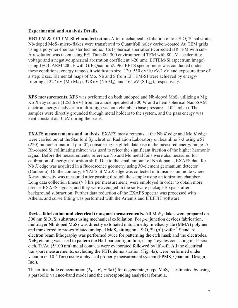
Experimental and Analysis Details. HRTEM & EFTEM-SI characterization. After mechanical exfoliation onto a SiO2/Si substrate, Nb-doped MoS2 micro-flakes were transferred to Quantifoil holey carbon-coated Au TEM grids using a polymer-free transfer technique.1 Cs (spherical aberration)-corrected HRTEM with sub-Å resolution was taken using FEI Titan 80–300 environmental TEM with 80 kV accelerating voltage and a negative spherical aberration coefficient (-20 µm). EFTEM-SI (spectrum image) using JEOL ARM 200cF with GIF Quantum® 965 EELS spectrometer was conducted under these conditions; energy range/slit width/step size: 120–550 eV/10 eV/1 eV and exposure time of a step: 2 sec. Elemental maps of Mo, Nb and S from EFTEM-SI were achieved by energy-filtering at 227 eV (Mo M4,5), 378 eV (Nb M2), and 165 eV (S L2,3), respectively.
XPS measurements. XPS was performed on both undoped and Nb-doped MoS2 utilizing a Mg Kα X-ray source (1253.6 eV) from an anode operated at 300 W and a hemispherical NanoSAM electron energy analyzer in a ultra-high vacuum chamber (base pressure ~ 10-10 mbar). The samples were directly grounded through metal holders to the system, and the pass energy was kept constant at 10 eV during the scans.
EXAFS measurements and analysis. EXAFS measurements at the Nb K edge and Mo K edge were carried out at the Stanford Synchrotron Radiation Laboratory on beamline 7-3 using a Si (220) monochromator at phi=0°, considering its glitch database in the measured energy range. A Rh-coated Si collimating mirror was used to reject the significant fraction of the higher harmonic signal. Before the measurements, reference Nb and Mo metal foils were also measured for calibration of energy absorption shift. Due to the small amount of Nb dopants, EXAFS data for Nb K edge was acquired in a fluorescence geometry using 30-element germanium detector (Canberra). On the contrary, EXAFS of Mo K edge was collected in transmission mode where X-ray intensity was measured after passing through the sample using an ionization chamber. Long data collection times (> 8 hrs per measurement) were employed in order to obtain more precise EXAFS signals, and they were averaged in the software package Sixpack after background subtraction. Further data reduction of the EXAFS spectra was processed with Athena, and curve fitting was performed with the Artemis and IFEFFIT software.
Device fabrication and electrical transport measurements. All MoS2 flakes were prepared on 300 nm SiO2/Si substrates using mechanical exfoliation. For p-n junction devices fabrication, multilayer Nb-doped MoS2 was directly exfoliated onto a methyl methacrylate (MMA) polymer and transferred to pre-exfoliated undoped MoS2 sitting on a SiO2/Si (p+) wafer.2 Standard electron beam lithography was performed twice for patterning the etch mask and the electrodes. XeF2 etching was used to pattern the Hall-bar configuration, using 4 cycles consisting of 15 sec etch. Ti/Au (5/100 nm) metal contacts were evaporated followed by lift-off. All the electrical transport measurements, excluding the FETs demonstration (Fig. 4a), were performed under vacuum (~ 10-3 Torr) using a physical property measurement system (PPMS, Quantum Design, Inc.). The critical hole concentration (EF ~ EV + 3kT) for degenerate p-type MoS2 is estimated by using a parabolic valence-band model and the corresponding analytical formula,
3
p = 2
mp*kT2π!2
⎡
⎣⎢
⎤
⎦⎥
3/2
e(EV −EF )kT . It was found to be approximately 7 × 1017 cm-3 using a hole effective
mass mp* of 0.68 mo.3 Therefore, our measured hole density far exceeds this value and justifies our explanation assuming a degenerate doping.
The ideality factor of the p-n junction presented in Fig. 4 is calculated by employing the curve
fitting to the Shockley ideal diode equation, Ids = Is eeVdsnkBT −1
⎛
⎝⎜⎞
⎠⎟. For Vg > +40 V where a
significant rectification has been observed, the diode ideality factor (n) is found to be 2 ~ 3 with r2 > 99%. This presumably implies the existence of charge trap states and disorder either within charge depletion region or at their interfaces.4
4
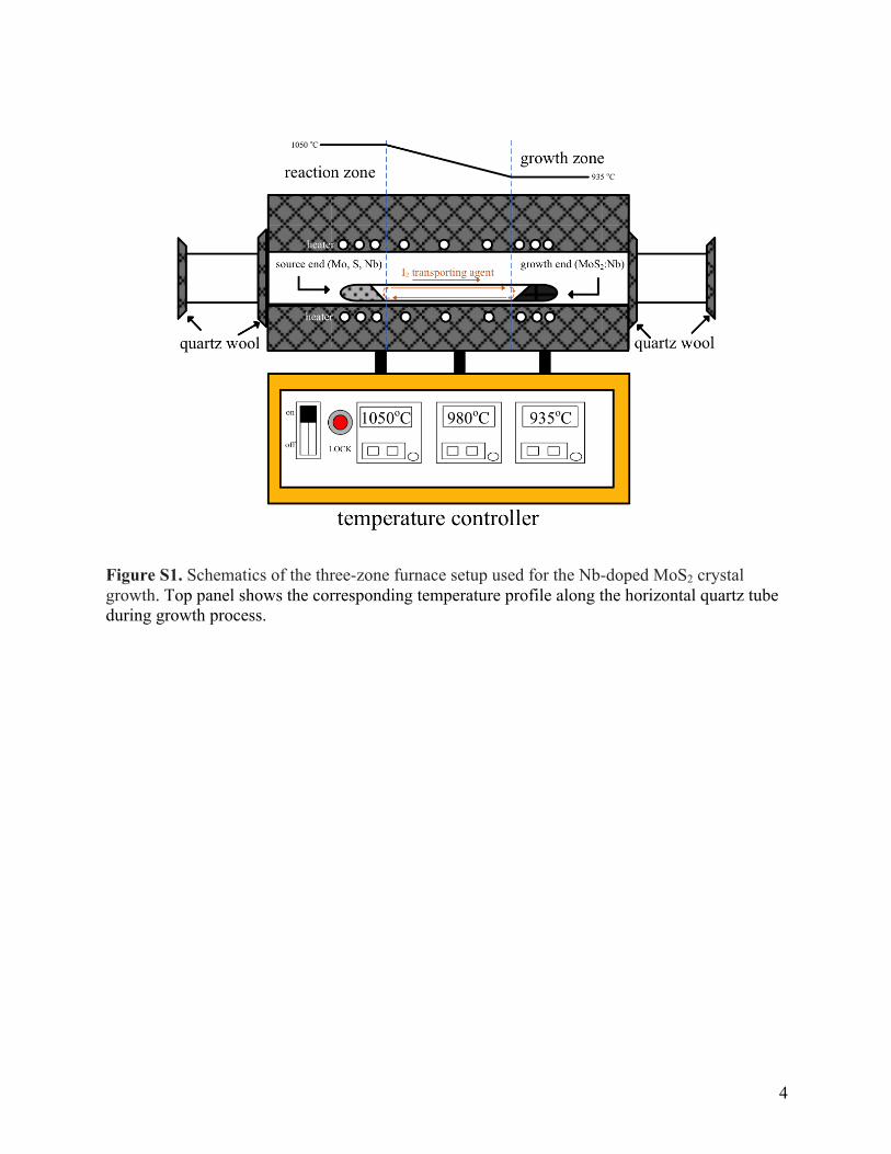
Figure S1. Schematics of the three-zone furnace setup used for the Nb-doped MoS2 crystal growth. Top panel shows the corresponding temperature profile along the horizontal quartz tube during growth process.
5
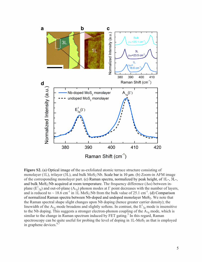
Figure S2. (a) Optical image of the as-exfoliated atomic terrace structure consisting of monolayer (1L), trilayer (3L), and bulk MoS2:Nb. Scale bar is 10 µm. (b) Zoom-in AFM image of the corresponding monolayer part. (c) Raman spectra, normalized by peak height, of 1L-, 3L-, and bulk MoS2:Nb acquired at room temperature. The frequency difference (Δω) between in-plane (E1
2g) and out-of-plane (A1g) phonon modes at Γ point decreases with the number of layers, and is reduced to ~ 18.6 cm-1 in 1L MoS2:Nb from the bulk value of 25.1 cm-1. (d) Comparison of normalized Raman spectra between Nb-doped and undoped monolayer MoS2. We note that the Raman spectral shape slight changes upon Nb doping (hence greater carrier density); the linewidth of the A1g mode broadens and slightly softens. In contrast, the E1
2g mode is insensitive to the Nb doping. This suggests a stronger electron-phonon coupling of the A1g mode, which is similar to the change in Raman spectrum induced by FET gating.5 In this regard, Raman spectroscopy can be quite useful for probing the level of doping in 1L-MoS2 as that is employed in graphene devices.6,7
6
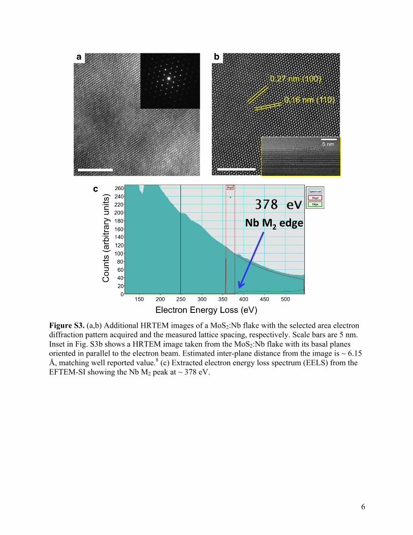
Figure S3. (a,b) Additional HRTEM images of a MoS2:Nb flake with the selected area electron diffraction pattern acquired and the measured lattice spacing, respectively. Scale bars are 5 nm. Inset in Fig. S3b shows a HRTEM image taken from the MoS2:Nb flake with its basal planes oriented in parallel to the electron beam. Estimated inter-plane distance from the image is ~ 6.15 Å, matching well reported value.8 (c) Extracted electron energy loss spectrum (EELS) from the EFTEM-SI showing the Nb M2 peak at ~ 378 eV.
7
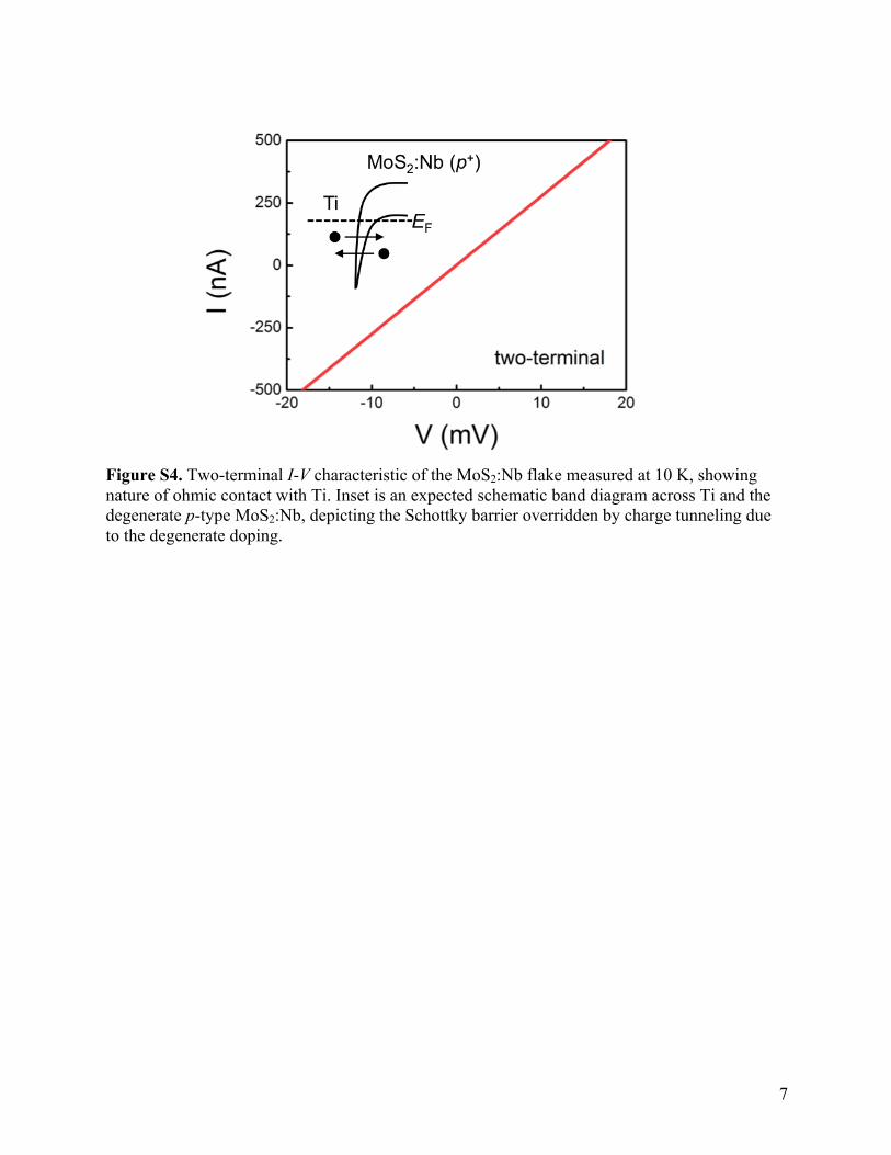
Figure S4. Two-terminal I-V characteristic of the MoS2:Nb flake measured at 10 K, showing nature of ohmic contact with Ti. Inset is an expected schematic band diagram across Ti and the degenerate p-type MoS2:Nb, depicting the Schottky barrier overridden by charge tunneling due to the degenerate doping.
8
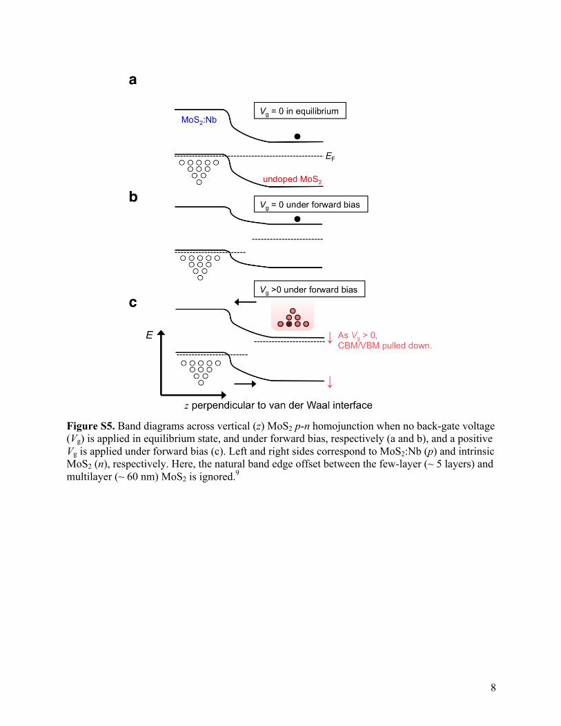
Figure S5. Band diagrams across vertical (z) MoS2 p-n homojunction when no back-gate voltage (Vg) is applied in equilibrium state, and under forward bias, respectively (a and b), and a positive Vg is applied under forward bias (c). Left and right sides correspond to MoS2:Nb (p) and intrinsic MoS2 (n), respectively. Here, the natural band edge offset between the few-layer (~ 5 layers) and multilayer (~ 60 nm) MoS2 is ignored.9
9
Figure S6. (a) Direct evidence of doping stability of a MoS2:Nb-based device with comparison of Rxx measured before and after one month in ambient. (b-c) Comparison of I-V rectification of the MoS2:Nb-based diode at various gating voltages before (b) and after (c) 7 days exposure to ambient air.
10
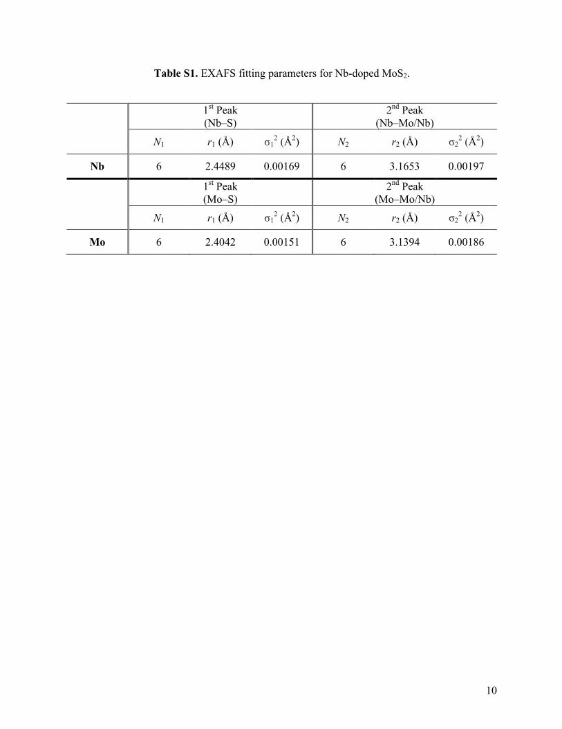
Table S1. EXAFS fitting parameters for Nb-doped MoS2.
1st Peak (Nb–S)
2nd Peak (Nb–Mo/Nb)
N1 r1 (Å) σ12 (Å2) N2 r2 (Å) σ2
2 (Å2)
Nb 6 2.4489 0.00169 6 3.1653 0.00197
1st Peak (Mo–S)
2nd Peak (Mo–Mo/Nb)
N1 r1 (Å) σ12 (Å2) N2 r2 (Å) σ2
2 (Å2)
Mo 6 2.4042 0.00151 6 3.1394 0.00186
11
References 1. Regan, W.; Alem, N.; Alemán, B.; Geng, B.; Girit, Ç.; Maserati, L.; Wang, F.; Crommie, M.; Zettl, A. Appl. Phys. Lett. 2010, 96, 113102. 2. Ju, L. et al. Nat. Nanotech. 2014, 9, 348–352. 3. Jin, W. et al. Phys. Rev. Lett. 2013, 111, 106801. 4. Jariwala, D.; Sangwan, V. K.; Wu, C.-C.; Prabhumirashi, P. L.; Geier, M. L.; Marks, T. J.; Lauhon, L. J.; Hersam, M. C. Proc. Natl. Acad. Sci. USA 2013, 110, 18076. 5. Chakraborty, B.; Bera, A.; Muthu, D. V. S.; Bhowmick, S.; Waghmare, U. V.; Sood, A. K. Phys. Rev. B 2012, 85, 161403(R). 6. Pisana, S.; Lazzeri, M.; Casiraghi, C.; Novoselov, K. S.; Geim, A. K.; Ferrari, A. C.; Mauri, F. Nat. Mater. 2007, 6, 198–201. 7. Das, A. Nat. Nanotech. 2008, 3, 210–215. 8. Stewart, J. A.; Spearot, D. E. Modelling Simul. Mater. Sci. Eng. 2013, 21, 045003. 9. Kang, J.; Tongay, S.; Zhou, J.; Li, J.; Wu, J. Appl. Phys. Lett. 2013, 102, 012111.


![WORLD ANTI-DOPING AGENCY and THE ANTI-DOPING ORGANIZATION · world anti-doping agency and the anti-doping organization [insert name] _____ agreement governing the use and sharing](https://img.pdfslide.us/doc/110x75/5c1bae9309d3f2826b8b8c64/world-anti-doping-agency-and-the-anti-doping-organization-world-anti-doping.jpg)
![Evidence for photogenerated intermediate hole polarons in ZnOth.fhi-berlin.mpg.de/site/uploads/Publications/51428_2_merged_1426091264.pdfdoping) [16]. Since spectra recorded after](https://img.pdfslide.us/doc/110x75/5f2338fd8255547b303deaeb/evidence-for-photogenerated-intermediate-hole-polarons-in-znothfhi-doping-16.jpg)